EP0503200A2 - Package for microwave integrated circuit - Google Patents
Package for microwave integrated circuit Download PDFInfo
- Publication number
- EP0503200A2 EP0503200A2 EP91311833A EP91311833A EP0503200A2 EP 0503200 A2 EP0503200 A2 EP 0503200A2 EP 91311833 A EP91311833 A EP 91311833A EP 91311833 A EP91311833 A EP 91311833A EP 0503200 A2 EP0503200 A2 EP 0503200A2
- Authority
- EP
- European Patent Office
- Prior art keywords
- layer
- package
- integrated circuit
- microwave integrated
- grounding metal
- Prior art date
- Legal status (The legal status is an assumption and is not a legal conclusion. Google has not performed a legal analysis and makes no representation as to the accuracy of the status listed.)
- Granted
Links
Images


Classifications
-
- H—ELECTRICITY
- H01—ELECTRIC ELEMENTS
- H01L—SEMICONDUCTOR DEVICES NOT COVERED BY CLASS H10
- H01L23/00—Details of semiconductor or other solid state devices
- H01L23/58—Structural electrical arrangements for semiconductor devices not otherwise provided for, e.g. in combination with batteries
- H01L23/64—Impedance arrangements
- H01L23/66—High-frequency adaptations
-
- H—ELECTRICITY
- H01—ELECTRIC ELEMENTS
- H01L—SEMICONDUCTOR DEVICES NOT COVERED BY CLASS H10
- H01L2224/00—Indexing scheme for arrangements for connecting or disconnecting semiconductor or solid-state bodies and methods related thereto as covered by H01L24/00
- H01L2224/01—Means for bonding being attached to, or being formed on, the surface to be connected, e.g. chip-to-package, die-attach, "first-level" interconnects; Manufacturing methods related thereto
- H01L2224/42—Wire connectors; Manufacturing methods related thereto
- H01L2224/47—Structure, shape, material or disposition of the wire connectors after the connecting process
- H01L2224/48—Structure, shape, material or disposition of the wire connectors after the connecting process of an individual wire connector
- H01L2224/4805—Shape
- H01L2224/4809—Loop shape
- H01L2224/48091—Arched
-
- H—ELECTRICITY
- H01—ELECTRIC ELEMENTS
- H01L—SEMICONDUCTOR DEVICES NOT COVERED BY CLASS H10
- H01L2224/00—Indexing scheme for arrangements for connecting or disconnecting semiconductor or solid-state bodies and methods related thereto as covered by H01L24/00
- H01L2224/01—Means for bonding being attached to, or being formed on, the surface to be connected, e.g. chip-to-package, die-attach, "first-level" interconnects; Manufacturing methods related thereto
- H01L2224/42—Wire connectors; Manufacturing methods related thereto
- H01L2224/47—Structure, shape, material or disposition of the wire connectors after the connecting process
- H01L2224/48—Structure, shape, material or disposition of the wire connectors after the connecting process of an individual wire connector
- H01L2224/481—Disposition
- H01L2224/48151—Connecting between a semiconductor or solid-state body and an item not being a semiconductor or solid-state body, e.g. chip-to-substrate, chip-to-passive
- H01L2224/48221—Connecting between a semiconductor or solid-state body and an item not being a semiconductor or solid-state body, e.g. chip-to-substrate, chip-to-passive the body and the item being stacked
- H01L2224/48225—Connecting between a semiconductor or solid-state body and an item not being a semiconductor or solid-state body, e.g. chip-to-substrate, chip-to-passive the body and the item being stacked the item being non-metallic, e.g. insulating substrate with or without metallisation
- H01L2224/48227—Connecting between a semiconductor or solid-state body and an item not being a semiconductor or solid-state body, e.g. chip-to-substrate, chip-to-passive the body and the item being stacked the item being non-metallic, e.g. insulating substrate with or without metallisation connecting the wire to a bond pad of the item
-
- H—ELECTRICITY
- H01—ELECTRIC ELEMENTS
- H01L—SEMICONDUCTOR DEVICES NOT COVERED BY CLASS H10
- H01L2224/00—Indexing scheme for arrangements for connecting or disconnecting semiconductor or solid-state bodies and methods related thereto as covered by H01L24/00
- H01L2224/01—Means for bonding being attached to, or being formed on, the surface to be connected, e.g. chip-to-package, die-attach, "first-level" interconnects; Manufacturing methods related thereto
- H01L2224/42—Wire connectors; Manufacturing methods related thereto
- H01L2224/47—Structure, shape, material or disposition of the wire connectors after the connecting process
- H01L2224/49—Structure, shape, material or disposition of the wire connectors after the connecting process of a plurality of wire connectors
- H01L2224/491—Disposition
- H01L2224/4912—Layout
- H01L2224/49175—Parallel arrangements
-
- H—ELECTRICITY
- H01—ELECTRIC ELEMENTS
- H01L—SEMICONDUCTOR DEVICES NOT COVERED BY CLASS H10
- H01L24/00—Arrangements for connecting or disconnecting semiconductor or solid-state bodies; Methods or apparatus related thereto
- H01L24/01—Means for bonding being attached to, or being formed on, the surface to be connected, e.g. chip-to-package, die-attach, "first-level" interconnects; Manufacturing methods related thereto
- H01L24/42—Wire connectors; Manufacturing methods related thereto
- H01L24/47—Structure, shape, material or disposition of the wire connectors after the connecting process
- H01L24/48—Structure, shape, material or disposition of the wire connectors after the connecting process of an individual wire connector
-
- H—ELECTRICITY
- H01—ELECTRIC ELEMENTS
- H01L—SEMICONDUCTOR DEVICES NOT COVERED BY CLASS H10
- H01L24/00—Arrangements for connecting or disconnecting semiconductor or solid-state bodies; Methods or apparatus related thereto
- H01L24/01—Means for bonding being attached to, or being formed on, the surface to be connected, e.g. chip-to-package, die-attach, "first-level" interconnects; Manufacturing methods related thereto
- H01L24/42—Wire connectors; Manufacturing methods related thereto
- H01L24/47—Structure, shape, material or disposition of the wire connectors after the connecting process
- H01L24/49—Structure, shape, material or disposition of the wire connectors after the connecting process of a plurality of wire connectors
-
- H—ELECTRICITY
- H01—ELECTRIC ELEMENTS
- H01L—SEMICONDUCTOR DEVICES NOT COVERED BY CLASS H10
- H01L2924/00—Indexing scheme for arrangements or methods for connecting or disconnecting semiconductor or solid-state bodies as covered by H01L24/00
- H01L2924/0001—Technical content checked by a classifier
- H01L2924/00014—Technical content checked by a classifier the subject-matter covered by the group, the symbol of which is combined with the symbol of this group, being disclosed without further technical details
-
- H—ELECTRICITY
- H01—ELECTRIC ELEMENTS
- H01L—SEMICONDUCTOR DEVICES NOT COVERED BY CLASS H10
- H01L2924/00—Indexing scheme for arrangements or methods for connecting or disconnecting semiconductor or solid-state bodies as covered by H01L24/00
- H01L2924/01—Chemical elements
- H01L2924/01078—Platinum [Pt]
-
- H—ELECTRICITY
- H01—ELECTRIC ELEMENTS
- H01L—SEMICONDUCTOR DEVICES NOT COVERED BY CLASS H10
- H01L2924/00—Indexing scheme for arrangements or methods for connecting or disconnecting semiconductor or solid-state bodies as covered by H01L24/00
- H01L2924/01—Chemical elements
- H01L2924/01079—Gold [Au]
-
- H—ELECTRICITY
- H01—ELECTRIC ELEMENTS
- H01L—SEMICONDUCTOR DEVICES NOT COVERED BY CLASS H10
- H01L2924/00—Indexing scheme for arrangements or methods for connecting or disconnecting semiconductor or solid-state bodies as covered by H01L24/00
- H01L2924/095—Indexing scheme for arrangements or methods for connecting or disconnecting semiconductor or solid-state bodies as covered by H01L24/00 with a principal constituent of the material being a combination of two or more materials provided in the groups H01L2924/013 - H01L2924/0715
- H01L2924/097—Glass-ceramics, e.g. devitrified glass
- H01L2924/09701—Low temperature co-fired ceramic [LTCC]
-
- H—ELECTRICITY
- H01—ELECTRIC ELEMENTS
- H01L—SEMICONDUCTOR DEVICES NOT COVERED BY CLASS H10
- H01L2924/00—Indexing scheme for arrangements or methods for connecting or disconnecting semiconductor or solid-state bodies as covered by H01L24/00
- H01L2924/10—Details of semiconductor or other solid state devices to be connected
- H01L2924/11—Device type
- H01L2924/14—Integrated circuits
-
- H—ELECTRICITY
- H01—ELECTRIC ELEMENTS
- H01L—SEMICONDUCTOR DEVICES NOT COVERED BY CLASS H10
- H01L2924/00—Indexing scheme for arrangements or methods for connecting or disconnecting semiconductor or solid-state bodies as covered by H01L24/00
- H01L2924/15—Details of package parts other than the semiconductor or other solid state devices to be connected
- H01L2924/161—Cap
- H01L2924/1615—Shape
- H01L2924/16195—Flat cap [not enclosing an internal cavity]
-
- H—ELECTRICITY
- H01—ELECTRIC ELEMENTS
- H01L—SEMICONDUCTOR DEVICES NOT COVERED BY CLASS H10
- H01L2924/00—Indexing scheme for arrangements or methods for connecting or disconnecting semiconductor or solid-state bodies as covered by H01L24/00
- H01L2924/30—Technical effects
- H01L2924/301—Electrical effects
- H01L2924/30107—Inductance
-
- H—ELECTRICITY
- H01—ELECTRIC ELEMENTS
- H01L—SEMICONDUCTOR DEVICES NOT COVERED BY CLASS H10
- H01L2924/00—Indexing scheme for arrangements or methods for connecting or disconnecting semiconductor or solid-state bodies as covered by H01L24/00
- H01L2924/30—Technical effects
- H01L2924/301—Electrical effects
- H01L2924/3011—Impedance
-
- H—ELECTRICITY
- H01—ELECTRIC ELEMENTS
- H01L—SEMICONDUCTOR DEVICES NOT COVERED BY CLASS H10
- H01L2924/00—Indexing scheme for arrangements or methods for connecting or disconnecting semiconductor or solid-state bodies as covered by H01L24/00
- H01L2924/30—Technical effects
- H01L2924/301—Electrical effects
- H01L2924/3025—Electromagnetic shielding
Definitions
- the present invention relates to a package for a semiconductor device operating at high frequency of more than several tens MHz and, more particularly, to a package for a microwave integrated circuit (hereinafter referred to as IC) in which an intermediate-layer grounding metal is provided on the same plane as that on which a transmission line is provided and an upper-layer grounding metal, the intermediate-layer grounding metal, and a lower-layer grounding metal are connected with one another via through holes.
- IC microwave integrated circuit
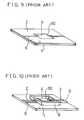
- FIGS 9(a) and 9(b) are perspective views illustrating a prior art micro-strip type chip carrier.
- reference numeral 1 designates a grounding metal base comprising such as copper-tungsten.
- a dielectric layer 2 comprising ceramic is provided on the grounding metal base 1.
- a transmission line 6 is provided on the surface of the dielectric layer 2.
- the dielectric layer 2 insulates the transmission line 6 from the grounding metal base 1.
- the dielectric layer 2 has an aperture in the center thereof, in which an IC chip bonding part 4 for bonding a microwave IC chip 30 is provided.
- the rear surface of the IC chip bonding part 4 is connected to the grounding metal base 1.
- the IC chip 30 is fixed on the IC chip bonding part 4 by solder or adhesive. An electric signal is transmitted through the transmission line 6 to the IC chip 30.
- this package has an advantage in that the parasitic capacitance and parasitic inductance are shielded, it has a disadvantage in that airtightness is poor because it cannot be hermetically sealed due to its configuration.
- the IC chip 30 and wires are exposed and this package has, in particular, no durability against the mechanical breakage. Therefore, it cannot be used in applications which requires reliability of the package.
- the frequency range capable of being used is approximately up to 30 GHz.
- FIG 10 is a perspective view illustrating a structure of a prior art dielectric material feed-through type metal package.
- Figure 12 is a perspective view illustrating the package of figure 10 which is hermetically sealed.
- reference numeral 1 designates a grounding metal base.
- a transmission line 6 is provided on the grounding metal base 1. This transmission line 6 is insulated from the grounding metal base 1 by a ceramic dielectric material layer 2.
- An IC chip bonding part 4 for bonding an IC chip 30 is provided in the aperture formed in the center of the grounding metal base 1, and a ring metal cavity 8 is provided surrounding the IC chip 30.
- the IC chip 30 is fixed on the IC chip bonding part 4 by solder or adhesive. An electric signal is transmitted through the transmission line 6 to the chip 30. As shown in figure 12, a metal lid 7 is put on the cavity 8, protecting the IC chip 30 and securing the airtightness.
- This package has advantages of high airtightness, good shielding property, and enhanced high frequency characteristic, so that it can be used at up to 20 GHz. However, it has a disadvantage in that the production cost is extremely high.
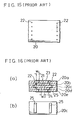
- Figure 11 is a perspective view illustrating a structure of a prior art tri-plate type multi-layer ceramic package.
- Figure 13 is a side view illustrating the package of figure 11 which is hermetically sealed.
- a lower-side dielectric layer 2b is provided on a lower-layer grounding metal 1b and an upper-layer grounding metal 1a is provided on an upper-side dielectric layer 2a.
- a transmission line 6 is provided on the junction surface between the lower-side dielectric layer 2b and the upper-side dielectric layer 2a.
- An IC chip bonding part 4 for fixing an IC chip 30 is provided in the aperture formed in the center of the upper-layer grounding metal 1a and the upper-side dielectric layer 2a. The IC chip bonding part 4 is connected to the lower-layer grounding metal 1b to be grounded via a through hole.
- the IC chip 30 is fixed on the IC chip bonding part 4 by solder or adhesive. Then, as shown in figure 13, a metal lid 7 is put on the package, protecting the IC chip 30 and securing the airtightness.
- This package has a merit of low production cost, approximately 1000 yen per one.
- the upper-layer grounding metal 1a and the lower-layer grounding metal 1b are not directly in contact with each other, when metal is plated on the side surface of the package to connect the two grounding metals 1a and 1b, the perimeter of the metal layer surrounding the transmission line 6 in the cross section vertical to the transmission line 6 is so long that the inductance component increases, deteriorating the shielding characteristic and the high frequency characteristic. Therefore, this package is used only at up to several GHz.
- Figure 14(a) is an exploded view illustrating a structure of this prior art package.
- Figure 14(b) is a cross-sectional view taken along a line A - A in figure 14(a).
- a ceramic layer 20b is provided on a lower-layer grounding metal 24 and a signal conductor 21 is provided in the center of the surface of the ceramic layer 20b.
- a ceramic layer 20a having a cut-off portion for exposing the signal conductor 21 is provided on the ceramic layer 20b.
- a plurality of cylindrical through holes 22 are provided penetrating the ceramic layers 20a and 20b.
- the through holes 22 are those for electrically conducting the upper surface of the ceramic layers with the lower surfaces of the ceramic layers.
- An upper-layer grounding plate 23 is provided on the ceramic layer 20a. The upper-layer grounding metal 23 and the lower-layer grounding metal 24 are connected to each other via the through holes 22 thereby to shield the signal conductor 21.
- Figure 15 is a plan view illustrating a structure of an alternative of the package shown in figure 14.
- the cylindrical through holes 22 are provided closely to each other, resulting in an enhancement of the shielding characteristic.
- Figure 16(a) is a cross-sectional side view illustrating a structure of another alternative of the package shown in figure 14.
- Figure 16(b) is a plan view illustrating a ceramic layer 20c of the package shown in figure 16(a).
- a plurality of cylindrical through holes 22 are produced penetrating the ceramic layers 20a to 20e and arranged at slightly different positions to produce a pseud coaxial configuration, and the upper surface of a through hole (22) conductor and the lower surface of another through hole (22) conductor are electrically conducted by a metal plate 25 which is provided therebetween.
- micro-strip type chip carrier shown in figure 9 cannot be sealed up due to its construction, no good airtightness is obtained. In addition, since the chip and the wire of the package are exposed, the package has no durability against mechanical breakage. Therefore, it is impossible to use the package of figure 9 for applications which require reliability.
- the dielectric feed-through type metal package shown in figure 10 has a good shielding characteristic and a high-frequency characteristic, but the production cost thereof is extremely high.
- the inductance component may be increased due to its length, deteriorating the shielding characteristic and the high-frequency characteristic.
- the package shown in figures 14 and 15 is shielded by the through holes, but the shielding in the horizontal direction to the signal line is not sufficient.
- the present invention is directed to solving the above described problems and has for its object to provide an IC package which has a good shielding characteristic and a high frequency characteristic and can be produced at low cost.
- a microwave IC package comprises a first intermediate-layer grounding metal and a transmission line which are produced on the same plane to form a co-planar type line, an upper-layer grounding metal and a lower-layer grounding metal which are provided above and below the intermediate-layer grounding metal to form a tri-plate type line, and through holes provided for connecting all the grounding metals. Therefore, the transmission line is shielded in the vicinity thereof in the horizontal direction to the transmission line, whereby the perimeter of the shielding metal in the cross section vertical to the transmission line is shortened. As a result, the inductance component is suppressed.
- the width of the intermediate-layer grounding metal is three to five times as that of the transmission line. Therefore, a leakage of the electric line of force can be reduced and the high frequency characteristic can be improved.
- a second intermediate-layer grounding metal is provided at least one of positions between the upper-layer grounding metal and the first intermediate-layer grounding metal or between the first intermediate-layer grounding metal and the lower-layer grounding metal, and all the grounding metals are connected to one another via the through holes. Therefore, the shielding characteristic and the high frequency characteristic of the package can be further improved.
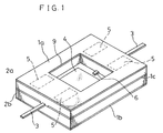
- Figure 1 is a perspective view illustrating a structure of a microwave IC tri-plate type multi-layer ceramic package in accordance with a first embodiment of the present invention.
- Figure 2 is a plan view of the microwave IC tri-plate type multi-layer ceramic package of figure 1 and figure 3 is a side view thereof.
- Figure 7 is a side view illustrating a cross section of the microwave IC tri-plate type multi-layer ceramic package of figure 1 on which an IC chip 30 is mounted.
- Figure 8 is a plan view illustrating a cross-section of the microwave IC package of figure 1 on which the IC chip 30 is mounted.
- a lower dielectric layer 2b is provided on a lower-layer grounding metal 1b.
- a transmission line 6 which inputs and outputs signals to the IC chip 30 is provided on the lower dielectric layer 2b.
- An intermediate-layer grounding metal 1c is provided on the same plane as that on which the transmission line 6 is provided, thereby forming a co-planar type line.
- an upper dielectric layer 2a and an upper-layer grounding metal 1a are produced on the intermediate-layer grounding metal 1c, thereby forming a tri-plate type line.
- gold electrolytic plating
- tungsten simple, gold-plated tungsten or the like is used as the grounding metal.
- An IC chip bonding part 4 is provided in the aperture 9 formed in the center of the upper dielectric layer 2a and the upper-layer grounding metal 1a.
- a metal film is plated on the side walls of the aperture 9 to shield the IC chip 30 in accordance with the performance to be pursued or the production cost of the device.
- the IC chip bonding part 4 is connected to the lower-layer grounding metal 1b via through holes 5a.
- the IC chip bonding part 4 comprises material such as gold-plated titanium or gold-plated AlN (aluminum nitride).
- the upper-layer, intermediate-layer, and lower-layer grounding metals 1a, 1c, and 1b are electrically connected to one another via the through holes 5.
- the IC chip 30 is shielded by the through holes 5 surrounding the chip. Furthermore, the rear surface of the IC chip bonding part 4 is connected to the lower-layer grounding metal 1b via the through holes 5a.
- the IC chip 30 is bonded on the IC chip bonding part 4 using solder, adhesive or the like, and then the transmission line 6, which is insulated, is produced on the dielectric layer 2 comprising ceramic.
- a metal lid 7 is put on the package, as shown in figure 4, to protect the IC chip 30 and to keep the airtightness.
- the intermediate-layer grounding metal 1c and the transmission line 6 form the co-planar type line
- the upper-layer, intermediate-layer, and lower-layer grounding metals 1a, 1c, and 1b form the tri-plate type line
- these three grounding metals are connected to one another via the through holes. Therefore, the perimeter of the shielding metal surrounding the transmission line 6 in the cross-section vertical to the transmission line 6 is shortened and the vicinity of the transmission line 6 is shielded by the through holes 5 in the horizontal direction to the transmission line 6, resulting in large improvements in the shielding characteristic and the high frequency characteristic.
- the package having such structure can be practically used at 18 to 30 GHz. In addition, this package can be easily produced because of its simple structure, low production cost, and low material cost.
- the package in accordance with the first embodiment has the following aspects and advantages as compared with the prior art IC package shown in figure 16. That is, in this embodiment, a plurality of through holes 5 are produced at the both sides of the transmission line 6 to form the pseud coaxial line configuration similarly as in the prior art device of figure 16 and further the through holes 5 are provided closer to the transmission line 6 than that of the prior art device, thereby improving the shielding characteristic and the high frequency characteristic.
- the width of the metal layer connecting between through holes that is, the width W2 of the intermediate-layer grounding metal is three to five times as the width W1 of the transmission line 6, whereby a leakage of the electric line of force can be reduced and the transmission loss and the deterioration of voltage standing wave ratio, which are caused by a high transmission mode, can be prevented.
- the IC chip 30 can be easily sealed up using this package as shown in figure 4. Consequently, the IC package having good shielding characteristic and high-frequency characteristic can be obtained at low production cost.
- Figure 5 is a cross-sectional view showing a tri-plate type multi-layer ceramic package in which an IC chip 30 is sealed up in accordance with a second embodiment of the present invention.
- Figures 6(a) to 6(f) are perspective views showing structures of respective layers of the tri-plate type multi-layer ceramic package of figure 5.
- reference characters 1c1 and 1c2 designate intermediate-layer grounding metals.
- a plurality of intermediate-layer grounding metals 1c to 1c2 are produced, whereby the package has a large number of grounding surfaces than the package of the first embodiment, enhancing the shielding characteristic and the high frequency characteristic.
- LFM low temperature firing material including glass
- AlN aluminum nitride
- PTFE porous Teflon
- a microwave IC package comprises a first intermediate-layer grounding metal and a transmission line produced on the same surface to form a co-planar type line, an upper and a lower-layer grounding metals which are provided above and below the first intermediate-layer grounding metal to form a tri-plate type line, and through holes for connecting all the three grounding metals. Therefore, the transmission line is shielded in the vicinity thereof in the direction horizontal to the transmission line, and further, the perimeter of the shielding metal in the cross section vertical to the transmission line is shortened. As a result, inductance component is suppressed.
- the width of the intermediate-layer grounding metal is three to five times as that of the transmission line, the leakage of the electric line of force is reduced, whereby the shielding characteristic and the high frequency characteristic are improved.
- the package can be produced at a low production cost.
- a second intermediate-layer grounding metal is produced at least one of positions between the upper and the first intermediate-layer grounding metals and between the first intermediate-layer and the lower-layer grounding metals and the all grounding metals are connected to one another via through holes. Therefore, the shielding characteristic can be further improved with the effects described above.
Abstract
Description
- The present invention relates to a package for a semiconductor device operating at high frequency of more than several tens MHz and, more particularly, to a package for a microwave integrated circuit (hereinafter referred to as IC) in which an intermediate-layer grounding metal is provided on the same plane as that on which a transmission line is provided and an upper-layer grounding metal, the intermediate-layer grounding metal, and a lower-layer grounding metal are connected with one another via through holes.
- Figures 9(a) and 9(b) are perspective views illustrating a prior art micro-strip type chip carrier. In these figures, reference numeral 1 designates a grounding metal base comprising such as copper-tungsten. A
dielectric layer 2 comprising ceramic is provided on the grounding metal base 1. Atransmission line 6 is provided on the surface of thedielectric layer 2. Thedielectric layer 2 insulates thetransmission line 6 from the grounding metal base 1. Thedielectric layer 2 has an aperture in the center thereof, in which an IC chip bondingpart 4 for bonding amicrowave IC chip 30 is provided. The rear surface of the ICchip bonding part 4 is connected to the grounding metal base 1. - The
IC chip 30 is fixed on the ICchip bonding part 4 by solder or adhesive. An electric signal is transmitted through thetransmission line 6 to theIC chip 30. Although this package has an advantage in that the parasitic capacitance and parasitic inductance are shielded, it has a disadvantage in that airtightness is poor because it cannot be hermetically sealed due to its configuration. In addition, theIC chip 30 and wires are exposed and this package has, in particular, no durability against the mechanical breakage. Therefore, it cannot be used in applications which requires reliability of the package. The frequency range capable of being used is approximately up to 30 GHz. - Figure 10 is a perspective view illustrating a structure of a prior art dielectric material feed-through type metal package. Figure 12 is a perspective view illustrating the package of figure 10 which is hermetically sealed. In figures 10 and 12, reference numeral 1 designates a grounding metal base. A
transmission line 6 is provided on the grounding metal base 1. Thistransmission line 6 is insulated from the grounding metal base 1 by a ceramicdielectric material layer 2. An ICchip bonding part 4 for bonding anIC chip 30 is provided in the aperture formed in the center of the grounding metal base 1, and aring metal cavity 8 is provided surrounding theIC chip 30. - The
IC chip 30 is fixed on the ICchip bonding part 4 by solder or adhesive. An electric signal is transmitted through thetransmission line 6 to thechip 30. As shown in figure 12, ametal lid 7 is put on thecavity 8, protecting theIC chip 30 and securing the airtightness. This package has advantages of high airtightness, good shielding property, and enhanced high frequency characteristic, so that it can be used at up to 20 GHz. However, it has a disadvantage in that the production cost is extremely high. - Figure 11 is a perspective view illustrating a structure of a prior art tri-plate type multi-layer ceramic package. Figure 13 is a side view illustrating the package of figure 11 which is hermetically sealed. In figures 11 and 13, a lower-side
dielectric layer 2b is provided on a lower-layer grounding metal 1b and an upper-layer grounding metal 1a is provided on an upper-sidedielectric layer 2a. Atransmission line 6 is provided on the junction surface between the lower-sidedielectric layer 2b and the upper-sidedielectric layer 2a. An ICchip bonding part 4 for fixing anIC chip 30 is provided in the aperture formed in the center of the upper-layer grounding metal 1a and the upper-sidedielectric layer 2a. The ICchip bonding part 4 is connected to the lower-layer grounding metal 1b to be grounded via a through hole. - The
IC chip 30 is fixed on the ICchip bonding part 4 by solder or adhesive. Then, as shown in figure 13, ametal lid 7 is put on the package, protecting theIC chip 30 and securing the airtightness. This package has a merit of low production cost, approximately 1000 yen per one. However, since the upper-layer grounding metal 1a and the lower-layer grounding metal 1b are not directly in contact with each other, when metal is plated on the side surface of the package to connect the twogrounding metals transmission line 6 in the cross section vertical to thetransmission line 6 is so long that the inductance component increases, deteriorating the shielding characteristic and the high frequency characteristic. Therefore, this package is used only at up to several GHz. - Meanwhile, a prior art package having a pseud coaxial line configuration is disclosed in the Japanese Published Patent Application No.1-135102. Figure 14(a) is an exploded view illustrating a structure of this prior art package. Figure 14(b) is a cross-sectional view taken along a line A - A in figure 14(a). In figures 14(a) and 14(b), a
ceramic layer 20b is provided on a lower-layer grounding metal 24 and asignal conductor 21 is provided in the center of the surface of theceramic layer 20b. Then, aceramic layer 20a having a cut-off portion for exposing thesignal conductor 21 is provided on theceramic layer 20b. A plurality of cylindrical throughholes 22 are provided penetrating theceramic layers holes 22 are those for electrically conducting the upper surface of the ceramic layers with the lower surfaces of the ceramic layers. An upper-layer grounding plate 23 is provided on theceramic layer 20a. The upper-layer grounding metal 23 and the lower-layer grounding metal 24 are connected to each other via the throughholes 22 thereby to shield thesignal conductor 21. - Figure 15 is a plan view illustrating a structure of an alternative of the package shown in figure 14. In this structure, the cylindrical through
holes 22 are provided closely to each other, resulting in an enhancement of the shielding characteristic. - Figure 16(a) is a cross-sectional side view illustrating a structure of another alternative of the package shown in figure 14. Figure 16(b) is a plan view illustrating a
ceramic layer 20c of the package shown in figure 16(a). In figures 16(a) and 16(b), a plurality of cylindrical throughholes 22 are produced penetrating theceramic layers 20a to 20e and arranged at slightly different positions to produce a pseud coaxial configuration, and the upper surface of a through hole (22) conductor and the lower surface of another through hole (22) conductor are electrically conducted by ametal plate 25 which is provided therebetween. - The prior art microwave IC packages constructed as described above have the following drawbacks.
- Since the micro-strip type chip carrier shown in figure 9 cannot be sealed up due to its construction, no good airtightness is obtained. In addition, since the chip and the wire of the package are exposed, the package has no durability against mechanical breakage. Therefore, it is impossible to use the package of figure 9 for applications which require reliability.
- The dielectric feed-through type metal package shown in figure 10 has a good shielding characteristic and a high-frequency characteristic, but the production cost thereof is extremely high.
- In the tri-plate type multiple layer ceramic package shown in figure 11, when the upper-layer and lower-layer metal plates are connected using metals plated on the side surfaces or external surfaces of the package, the inductance component may be increased due to its length, deteriorating the shielding characteristic and the high-frequency characteristic.
- The package shown in figures 14 and 15 is shielded by the through holes, but the shielding in the horizontal direction to the signal line is not sufficient.
- Furthermore, it is difficult to form the package of figure 16(a)in a pseud coaxial configuration by shifting the through holes and a simulation is required therefor. Since the width W₃ of signal line is almost equal to the width W₄ of the metal plate, leakage of the electric line of force increases, resulting in a transmission loss and a deterioration of voltage standing wave ratio caused by generation of higher transmission mode.
- The present invention is directed to solving the above described problems and has for its object to provide an IC package which has a good shielding characteristic and a high frequency characteristic and can be produced at low cost.
- Other objects and advantages of the present invention will become apparent from the detailed description given hereinafter; it should be understood, however, that the detailed description and specific embodiment are given by way of illustration only, since various changes and modifications within the spirit and the scope of the invention will become apparent to those skilled in the art from this detailed description.
- According to a first aspect of the present invention, a microwave IC package comprises a first intermediate-layer grounding metal and a transmission line which are produced on the same plane to form a co-planar type line, an upper-layer grounding metal and a lower-layer grounding metal which are provided above and below the intermediate-layer grounding metal to form a tri-plate type line, and through holes provided for connecting all the grounding metals. Therefore, the transmission line is shielded in the vicinity thereof in the horizontal direction to the transmission line, whereby the perimeter of the shielding metal in the cross section vertical to the transmission line is shortened. As a result, the inductance component is suppressed.
- According to a second aspect of the present invention, the width of the intermediate-layer grounding metal is three to five times as that of the transmission line. Therefore, a leakage of the electric line of force can be reduced and the high frequency characteristic can be improved.
- According to a third aspect of the present invention, a second intermediate-layer grounding metal is provided at least one of positions between the upper-layer grounding metal and the first intermediate-layer grounding metal or between the first intermediate-layer grounding metal and the lower-layer grounding metal, and all the grounding metals are connected to one another via the through holes. Therefore, the shielding characteristic and the high frequency characteristic of the package can be further improved.
-
- Figure 1 is a perspective view illustrating a structure of a microwave IC package comprising an intermediate-layer grounding metal in accordance with a first embodiment of the present invention;
- Figure 2 is a plan view illustrating the microwave IC package of figure 1;
- Figure 3 is a side view illustrating the microwave IC package of figure 1;
- Figure 4 is a side view illustrating the microwave IC package of figure 1 which is hermetically sealed;
- Figure 5 is a side view illustrating a microwave IC package comprising a plurality of intermediate-layer grounding metals, which is hermetically sealed, in accordance with a second embodiment of the present invention;
- Figures 6(a) to 6(f) are perspective views illustrating structures of respective layers of the microwave IC package of figure 5;
- Figure 7 is a side view illustrating a cross section of the microwave IC package of figure 1 on which an IC chip is mounted;
- Figure 8 is a plan view illustrating a cross section of the microwave IC package of figure 1 on which an IC chip is mounted;
- Figure 9 is a perspective view illustrating a structure of a prior art micro-strip type chip carrier;
- Figure 10 is a perspective view illustrating a structure of a prior art dielectric feed-through type metal package;
- Figure 11 is a perspective view illustrating a structure of a prior art tri-plate type multiple layer ceramic package;
- Figure 12 is a perspective view illustrating the prior art dielectric feed-through type metal package of figure 10 which is hermetically sealed;
- Figure 13 is a side view illustrating the prior art tri-plate type multiple layer ceramic package of figure 11 which is hermetically sealed;
- Figure 14(a) is an exploded view illustrating a structure of a prior art ceramic package using through holes and Figure 14(b) is a cross-sectional view thereof;
- Figure 15 is a plan view illustrating a structure of a prior art ceramic package in which through holes are provided closely to each other; and
- Figure 16(a) is a cross sectional view illustrating a structure of a prior art ceramic package in which through holes are provided at slightly different positions and Figure 16(b) is a plan view thereof.
-
- Figure 1 is a perspective view illustrating a structure of a microwave IC tri-plate type multi-layer ceramic package in accordance with a first embodiment of the present invention. Figure 2 is a plan view of the microwave IC tri-plate type multi-layer ceramic package of figure 1 and figure 3 is a side view thereof. Figure 7 is a side view illustrating a cross section of the microwave IC tri-plate type multi-layer ceramic package of figure 1 on which an
IC chip 30 is mounted. Figure 8 is a plan view illustrating a cross-section of the microwave IC package of figure 1 on which theIC chip 30 is mounted. In figures 1, 2, 3, 7 and 8, a lowerdielectric layer 2b is provided on a lower-layer grounding metal 1b. Atransmission line 6 which inputs and outputs signals to theIC chip 30 is provided on the lowerdielectric layer 2b. An intermediate-layer grounding metal 1c is provided on the same plane as that on which thetransmission line 6 is provided, thereby forming a co-planar type line. Furthermore, anupper dielectric layer 2a and an upper-layer grounding metal 1a are produced on the intermediate-layer grounding metal 1c, thereby forming a tri-plate type line. Ordinarily, gold (electrolytic plating), tungsten simple, gold-plated tungsten or the like is used as the grounding metal. An ICchip bonding part 4 is provided in theaperture 9 formed in the center of theupper dielectric layer 2a and the upper-layer grounding metal 1a. In some cases, a metal film is plated on the side walls of theaperture 9 to shield theIC chip 30 in accordance with the performance to be pursued or the production cost of the device. The ICchip bonding part 4 is connected to the lower-layer grounding metal 1b via throughholes 5a. The ICchip bonding part 4 comprises material such as gold-plated titanium or gold-plated AlN (aluminum nitride). The upper-layer, intermediate-layer, and lower-layer grounding metals IC chip 30 is shielded by the throughholes 5 surrounding the chip. Furthermore, the rear surface of the ICchip bonding part 4 is connected to the lower-layer grounding metal 1b via the throughholes 5a. - As shown in figure 7, the
IC chip 30 is bonded on the ICchip bonding part 4 using solder, adhesive or the like, and then thetransmission line 6, which is insulated, is produced on thedielectric layer 2 comprising ceramic. Ametal lid 7 is put on the package, as shown in figure 4, to protect theIC chip 30 and to keep the airtightness. - In the above-described first embodiment, the intermediate-
layer grounding metal 1c and thetransmission line 6 form the co-planar type line, and the upper-layer, intermediate-layer, and lower-layer grounding metals transmission line 6 in the cross-section vertical to thetransmission line 6 is shortened and the vicinity of thetransmission line 6 is shielded by the throughholes 5 in the horizontal direction to thetransmission line 6, resulting in large improvements in the shielding characteristic and the high frequency characteristic. The package having such structure can be practically used at 18 to 30 GHz. In addition, this package can be easily produced because of its simple structure, low production cost, and low material cost. - The package in accordance with the first embodiment has the following aspects and advantages as compared with the prior art IC package shown in figure 16. That is, in this embodiment, a plurality of through
holes 5 are produced at the both sides of thetransmission line 6 to form the pseud coaxial line configuration similarly as in the prior art device of figure 16 and further the throughholes 5 are provided closer to thetransmission line 6 than that of the prior art device, thereby improving the shielding characteristic and the high frequency characteristic. Furthermore, as shown in figure 4, the width of the metal layer connecting between through holes, that is, the width W₂ of the intermediate-layer grounding metal is three to five times as the width W₁ of thetransmission line 6, whereby a leakage of the electric line of force can be reduced and the transmission loss and the deterioration of voltage standing wave ratio, which are caused by a high transmission mode, can be prevented. Furthermore, theIC chip 30 can be easily sealed up using this package as shown in figure 4. Consequently, the IC package having good shielding characteristic and high-frequency characteristic can be obtained at low production cost. - Figure 5 is a cross-sectional view showing a tri-plate type multi-layer ceramic package in which an
IC chip 30 is sealed up in accordance with a second embodiment of the present invention. Figures 6(a) to 6(f) are perspective views showing structures of respective layers of the tri-plate type multi-layer ceramic package of figure 5. In figures 5 and 6, reference characters 1c₁ and 1c₂ designate intermediate-layer grounding metals. - In this second embodiment, a plurality of intermediate-
layer grounding metals 1c to 1c₂ are produced, whereby the package has a large number of grounding surfaces than the package of the first embodiment, enhancing the shielding characteristic and the high frequency characteristic. - While in the above-described second embodiment a two-port package is described, the present invention may be applied to a three-port or more-port type package with the same effects as described above.
- While in the above-described embodiments ceramic is used as the
dielectric layer 2, LFM (low temperature firing material including glass), AlN (aluminum nitride), or PTFE (porous Teflon) can be used as the material therefor. - As is evident from the foregoing description, according to the present invention, a microwave IC package comprises a first intermediate-layer grounding metal and a transmission line produced on the same surface to form a co-planar type line, an upper and a lower-layer grounding metals which are provided above and below the first intermediate-layer grounding metal to form a tri-plate type line, and through holes for connecting all the three grounding metals. Therefore, the transmission line is shielded in the vicinity thereof in the direction horizontal to the transmission line, and further, the perimeter of the shielding metal in the cross section vertical to the transmission line is shortened. As a result, inductance component is suppressed.
- In addition, since the width of the intermediate-layer grounding metal is three to five times as that of the transmission line, the leakage of the electric line of force is reduced, whereby the shielding characteristic and the high frequency characteristic are improved. As well, the package can be produced at a low production cost.
- In addition, a second intermediate-layer grounding metal is produced at least one of positions between the upper and the first intermediate-layer grounding metals and between the first intermediate-layer and the lower-layer grounding metals and the all grounding metals are connected to one another via through holes. Therefore, the shielding characteristic can be further improved with the effects described above.
Claims (11)
- A package for a microwave integrated circuit, comprising:
a first dielectric material layer on the surface of which a microwave integrated circuit and a transmission line inputting or outputting a signal of said microwave integrated circuit are arranged;
a second dielectric material layer laminated on said first dielectric layer so as to surround said microwave integrated circuit;
a first grounding metal layer produced on the entire rear surface of said first dielectric layer;
a second grounding metal layer produced on said second dielectric layer;
a first intermediate-layer grounding metal produced on the same plane as that on which said transmission line is produced, forming a co-planar type line with said transmission line; and
through holes electrically connecting said intermediate-layer grounding metal with said first and second grounding metals. - A package for a microwave integrated circuit in accordance with claim 1 wherein said grounding metal layer comprises gold by electrolytic plating, tungsten, or gold-plated tungsten.
- A package for a microwave integrated circuit in accordance with claim 1 wherein said dielectric layer comprises ceramic, low temperature firing glass, aluminum nitride, or porous Teflon.
- A package for a microwave integrated circuit in accordance with claim 1 wherein an IC chip bonding part on which said microwave integrated circuit is bonded comprises gold-plated titanium or gold-plated aluminum nitride.
- A package for a microwave integrated circuit in accordance with claim 1 wherein a metal film is plated on the side wall of the central aperture of said upper dielectric layer and said upper-layer grounding metal thereby to shield the IC chip.
- A package for a microwave integrated circuit in accordance with claim 1 wherein said through holes electrically conduct between said grounding metal layers.
- A package for a microwave integrated circuit in accordance with claim 1 which can be practically used at 18 to 30 GHz.
- A package for a microwave integrated circuit in accordance with claim 1 wherein a plurality of through holes are arranged at both side vicinity of said transmission line so as to form a pseudo coaxial line configuration.
- A package for a microwave integrated circuit in accordance with claim 1 wherein the width of said intermediate-layer grounding metal is three to five times as that of said transmission line.
- A package for a microwave integrated circuit in accordance with any of the preceding claims 1-3, 5-9, further comprising:
a second intermediate-layer grounding metal produced on at least one of portions between said first grounding metal layer and said first intermediate-layer grounding metal and between said second grounding metal layer and said first intermediate-layer grounding metal; and
through holes electrically connecting these metal layers with each other. - A package for a microwave integrated circuit in accordance with claim 10 wherein an IC chip bonding part on which said microwave integrated circuit is bonded comprises titanium mixed with gold or aluminum nitride mixed with gold.
Applications Claiming Priority (2)
| Application Number | Priority Date | Filing Date | Title |
|---|---|---|---|
| JP3039518A JPH04256203A (en) | 1991-02-07 | 1991-02-07 | Package for microwave band ic |
| JP39518/91 | 1991-02-07 |
Publications (3)
| Publication Number | Publication Date |
|---|---|
| EP0503200A2 true EP0503200A2 (en) | 1992-09-16 |
| EP0503200A3 EP0503200A3 (en) | 1993-03-24 |
| EP0503200B1 EP0503200B1 (en) | 1997-04-16 |
Family
ID=12555266
Family Applications (1)
| Application Number | Title | Priority Date | Filing Date |
|---|---|---|---|
| EP91311833A Expired - Lifetime EP0503200B1 (en) | 1991-02-07 | 1991-12-19 | Package for microwave integrated circuit |
Country Status (4)
| Country | Link |
|---|---|
| US (1) | US5235208A (en) |
| EP (1) | EP0503200B1 (en) |
| JP (1) | JPH04256203A (en) |
| DE (1) | DE69125703T2 (en) |
Cited By (16)
| Publication number | Priority date | Publication date | Assignee | Title |
|---|---|---|---|---|
| EP0595346A1 (en) * | 1992-10-29 | 1994-05-04 | Nec Corporation | Composite microwave module assembly and its connection structure |
| EP0764995A1 (en) * | 1995-09-21 | 1997-03-26 | HE HOLDINGS, INC. dba HUGHES ELECTRONICS | Microwave shielding structures |
| GB2307102A (en) * | 1995-11-08 | 1997-05-14 | Fujitsu Ltd | High frequency module package |
| GB2313239A (en) * | 1996-05-16 | 1997-11-19 | Pyronix Ltd | Microwave circuit device |
| US5796165A (en) * | 1996-03-19 | 1998-08-18 | Matsushita Electronics Corporation | High-frequency integrated circuit device having a multilayer structure |
| EP0897256A1 (en) * | 1996-04-24 | 1999-02-17 | Okamura, Susumu | Semiconductor device |
| US5907185A (en) * | 1996-09-24 | 1999-05-25 | Sumitomo Electric Industries, Ltd. | Ceramic terminal block, hermetic sealed package, and complex semiconductor device |
| WO1999034443A1 (en) * | 1997-12-15 | 1999-07-08 | Stratedge Corporation | Ceramic microelectronics package with co-planar waveguide feed-through |
| WO2003077316A1 (en) * | 2002-03-13 | 2003-09-18 | Optillion Ab | Impedance matching |
| US7088089B2 (en) | 2002-02-08 | 2006-08-08 | Rohde & Schware Gmbh & Co. Kg | Power detector with constant voltage decoupling |
| FR2929069A1 (en) * | 2008-03-21 | 2009-09-25 | Thales Sa | ELECTROMAGNETIC CONTAINMENT MODULE FOR ELECTRONIC COMPONENTS |
| EP2409662A3 (en) * | 2007-07-30 | 2012-08-01 | Vivant Medical, Inc. | Electrosurgical systems and printed circuit boards for use therewith |
| US9529025B2 (en) | 2012-06-29 | 2016-12-27 | Covidien Lp | Systems and methods for measuring the frequency of signals generated by high frequency medical devices |
| US9636165B2 (en) | 2013-07-29 | 2017-05-02 | Covidien Lp | Systems and methods for measuring tissue impedance through an electrosurgical cable |
| US9872719B2 (en) | 2013-07-24 | 2018-01-23 | Covidien Lp | Systems and methods for generating electrosurgical energy using a multistage power converter |
| WO2019055438A1 (en) * | 2017-09-12 | 2019-03-21 | Knowles Cazenovia, Inc. | Vertical switched filter bank |
Families Citing this family (51)
| Publication number | Priority date | Publication date | Assignee | Title |
|---|---|---|---|---|
| JPH0637202A (en) * | 1992-07-20 | 1994-02-10 | Mitsubishi Electric Corp | Package for microwave ic |
| US5477137A (en) * | 1992-10-02 | 1995-12-19 | Motorola, Inc. | Probeable substrate substitute for a calibration standard and test fixture |
| US5557144A (en) * | 1993-01-29 | 1996-09-17 | Anadigics, Inc. | Plastic packages for microwave frequency applications |
| US5338970A (en) * | 1993-03-24 | 1994-08-16 | Intergraph Corporation | Multi-layered integrated circuit package with improved high frequency performance |
| JP2924583B2 (en) * | 1993-06-30 | 1999-07-26 | 日本電気株式会社 | Element-separated composite microwave circuit module |
| US5428327A (en) * | 1993-08-23 | 1995-06-27 | Itt Corporation | Microwave feedthrough apparatus |
| US6339191B1 (en) * | 1994-03-11 | 2002-01-15 | Silicon Bandwidth Inc. | Prefabricated semiconductor chip carrier |
| GB2288286A (en) * | 1994-03-30 | 1995-10-11 | Plessey Semiconductors Ltd | Ball grid array arrangement |
| US5541565A (en) * | 1995-05-22 | 1996-07-30 | Trw Inc. | High frequency microelectronic circuit enclosure |
| DE19601650A1 (en) * | 1996-01-18 | 1997-07-24 | Telefunken Microelectron | Arrangement for protecting electrical and electronic components against electrostatic discharge |
| US7321485B2 (en) | 1997-04-08 | 2008-01-22 | X2Y Attenuators, Llc | Arrangement for energy conditioning |
| US7336468B2 (en) | 1997-04-08 | 2008-02-26 | X2Y Attenuators, Llc | Arrangement for energy conditioning |
| US9054094B2 (en) | 1997-04-08 | 2015-06-09 | X2Y Attenuators, Llc | Energy conditioning circuit arrangement for integrated circuit |
| TW328645B (en) * | 1997-04-14 | 1998-03-21 | Chyng-Guang Juang | The package for dual mode micro/nano-meter wave IC |
| DE948049T1 (en) * | 1998-03-03 | 2000-08-17 | Tzuang Ching Kuang | Housing for integrated microwave or millimeter wave switching in dual mode |
| FR2776435B1 (en) * | 1998-03-19 | 2000-04-28 | Alsthom Cge Alcatel | BIG GAIN AMPLIFIER |
| US6140698A (en) * | 1998-12-21 | 2000-10-31 | Nortel Networks Corporation | Package for microwave and mm-wave integrated circuits |
| JP3609692B2 (en) * | 2000-05-24 | 2005-01-12 | 松下電器産業株式会社 | High frequency signal amplifying device and method for manufacturing the same |
| FI114585B (en) * | 2000-06-09 | 2004-11-15 | Nokia Corp | Transfer cable in multilayer structures |
| US6627992B2 (en) | 2001-05-21 | 2003-09-30 | Xytrans, Inc. | Millimeter wave (MMW) transceiver module with transmitter, receiver and local oscillator frequency multiplier surface mounted chip set |
| SE522857C2 (en) * | 2001-11-23 | 2004-03-09 | Optillion Ab | Heat controlled optoelectric unit |
| AU2002366190A1 (en) * | 2001-11-23 | 2003-06-10 | Optillion Ab | Optoelectrical transceiver |
| JP4005451B2 (en) * | 2002-08-29 | 2007-11-07 | 富士通株式会社 | Multilayer substrate and semiconductor device |
| JP2003204211A (en) * | 2002-09-30 | 2003-07-18 | Nec Corp | Microwave/millimeter wave circuit device |
| EP1609206B1 (en) | 2003-03-04 | 2010-07-28 | Rohm and Haas Electronic Materials, L.L.C. | Coaxial waveguide microstructures and methods of formation thereof |
| US7116557B1 (en) * | 2003-05-23 | 2006-10-03 | Sti Electronics, Inc. | Imbedded component integrated circuit assembly and method of making same |
| WO2005032808A1 (en) * | 2003-10-01 | 2005-04-14 | The Yokohama Rubber Co., Ltd. | Method of manufacturing radial tire for construction vehicle |
| US7630188B2 (en) | 2005-03-01 | 2009-12-08 | X2Y Attenuators, Llc | Conditioner with coplanar conductors |
| EP1939137B1 (en) | 2006-12-30 | 2016-08-24 | Nuvotronics, LLC | Three-dimensional microstructures and methods of formation thereof |
| EP1973190A1 (en) | 2007-03-20 | 2008-09-24 | Rohm and Haas Electronic Materials LLC | Integrated electronic components and methods of formation thereof |
| EP1973189B1 (en) | 2007-03-20 | 2012-12-05 | Nuvotronics, LLC | Coaxial transmission line microstructures and methods of formation thereof |
| US20110123783A1 (en) | 2009-11-23 | 2011-05-26 | David Sherrer | Multilayer build processses and devices thereof |
| JP5599351B2 (en) * | 2011-03-30 | 2014-10-01 | 三菱電機株式会社 | Board device for connector mounting |
| US8866300B1 (en) | 2011-06-05 | 2014-10-21 | Nuvotronics, Llc | Devices and methods for solder flow control in three-dimensional microstructures |
| US8814601B1 (en) | 2011-06-06 | 2014-08-26 | Nuvotronics, Llc | Batch fabricated microconnectors |
| WO2013010108A1 (en) | 2011-07-13 | 2013-01-17 | Nuvotronics, Llc | Methods of fabricating electronic and mechanical structures |
| JP2013089841A (en) * | 2011-10-20 | 2013-05-13 | Kyocer Slc Technologies Corp | Wiring board |
| US8946562B2 (en) * | 2012-01-18 | 2015-02-03 | Covidien Lp | Printed circuit boards including strip-line circuitry and methods of manufacturing same |
| US9277645B2 (en) | 2012-01-18 | 2016-03-01 | Covidien Lp | Method of manufacturing a printed circuit board |
| US9351395B2 (en) * | 2012-01-18 | 2016-05-24 | Covidien Lp | Printed circuit boards including strip-line circuitry and methods of manufacturing same |
| US9325044B2 (en) | 2013-01-26 | 2016-04-26 | Nuvotronics, Inc. | Multi-layer digital elliptic filter and method |
| US9306255B1 (en) * | 2013-03-15 | 2016-04-05 | Nuvotronics, Inc. | Microstructure including microstructural waveguide elements and/or IC chips that are mechanically interconnected to each other |
| US9306254B1 (en) | 2013-03-15 | 2016-04-05 | Nuvotronics, Inc. | Substrate-free mechanical interconnection of electronic sub-systems using a spring configuration |
| WO2015109208A2 (en) | 2014-01-17 | 2015-07-23 | Nuvotronics, Llc | Wafer scale test interface unit: low loss and high isolation devices and methods for high speed and high density mixed signal interconnects and contactors |
| US10847469B2 (en) | 2016-04-26 | 2020-11-24 | Cubic Corporation | CTE compensation for wafer-level and chip-scale packages and assemblies |
| US10511073B2 (en) | 2014-12-03 | 2019-12-17 | Cubic Corporation | Systems and methods for manufacturing stacked circuits and transmission lines |
| CN107484350A (en) * | 2017-09-14 | 2017-12-15 | 中国电子科技集团公司第十三研究所 | Microwave device and its assembly method |
| US10319654B1 (en) | 2017-12-01 | 2019-06-11 | Cubic Corporation | Integrated chip scale packages |
| CN111586964A (en) * | 2020-05-25 | 2020-08-25 | 上海航天电子通讯设备研究所 | LCP substrate-based high-density high-frequency microwave assembly preparation method and microwave assembly |
| CN112436242A (en) * | 2020-10-26 | 2021-03-02 | 中国电子科技集团公司第十三研究所 | High integrated microwave assembly |
| CN112533358A (en) * | 2020-11-24 | 2021-03-19 | 中国电子科技集团公司第十三研究所 | High-frequency microwave multilayer circuit board and high-frequency microwave assembly |
Citations (8)
| Publication number | Priority date | Publication date | Assignee | Title |
|---|---|---|---|---|
| WO1984001470A1 (en) * | 1982-10-05 | 1984-04-12 | Mayo Foundation | Leadless chip carrier for logic components |
| EP0249378A2 (en) * | 1986-06-02 | 1987-12-16 | Fujitsu Limited | Package for integrated circuit |
| EP0309942A2 (en) * | 1987-10-02 | 1989-04-05 | AT&T Corp. | Multilayer ceramic package with high frequency connections |
| US4890155A (en) * | 1986-10-25 | 1989-12-26 | Shinko Electric Industries Co., Ltd. | Package for mounting a semiconductor chip of ultra-high frequency |
| EP0396152A1 (en) * | 1985-03-30 | 1990-11-07 | Fujitsu Limited | Semiconductor device comprising a package |
| EP0408228A2 (en) * | 1989-07-11 | 1991-01-16 | Oxley Developments Company Limited | Ceramic package and component |
| GB2238911A (en) * | 1989-11-24 | 1991-06-12 | Mitsubishi Electric Corp | Shielding integrated circuits |
| EP0444820A2 (en) * | 1990-02-26 | 1991-09-04 | Raytheon Company | MMIC package and connection |
Family Cites Families (6)
| Publication number | Priority date | Publication date | Assignee | Title |
|---|---|---|---|---|
| JPS5864223A (en) * | 1981-10-15 | 1983-04-16 | Ishihara Sangyo Kaisha Ltd | Treatment of magnetic iron oxide |
| JPS60227448A (en) * | 1984-04-26 | 1985-11-12 | Nec Corp | Semiconductor device |
| JPS60251649A (en) * | 1984-05-28 | 1985-12-12 | Nec Corp | Ic package |
| JPH0728133B2 (en) * | 1986-05-02 | 1995-03-29 | 株式会社東芝 | Circuit board |
| JPS6397001A (en) * | 1986-10-13 | 1988-04-27 | Mitsubishi Electric Corp | Microwave semiconductor device |
| US4922324A (en) * | 1987-01-20 | 1990-05-01 | Kabushiki Kaisha Toshiba | Semiconductor integrated circuit device |
-
1991
- 1991-02-07 JP JP3039518A patent/JPH04256203A/en active Pending
- 1991-12-19 EP EP91311833A patent/EP0503200B1/en not_active Expired - Lifetime
- 1991-12-19 DE DE69125703T patent/DE69125703T2/en not_active Expired - Fee Related
-
1992
- 1992-01-13 US US07/819,974 patent/US5235208A/en not_active Expired - Fee Related
Patent Citations (8)
| Publication number | Priority date | Publication date | Assignee | Title |
|---|---|---|---|---|
| WO1984001470A1 (en) * | 1982-10-05 | 1984-04-12 | Mayo Foundation | Leadless chip carrier for logic components |
| EP0396152A1 (en) * | 1985-03-30 | 1990-11-07 | Fujitsu Limited | Semiconductor device comprising a package |
| EP0249378A2 (en) * | 1986-06-02 | 1987-12-16 | Fujitsu Limited | Package for integrated circuit |
| US4890155A (en) * | 1986-10-25 | 1989-12-26 | Shinko Electric Industries Co., Ltd. | Package for mounting a semiconductor chip of ultra-high frequency |
| EP0309942A2 (en) * | 1987-10-02 | 1989-04-05 | AT&T Corp. | Multilayer ceramic package with high frequency connections |
| EP0408228A2 (en) * | 1989-07-11 | 1991-01-16 | Oxley Developments Company Limited | Ceramic package and component |
| GB2238911A (en) * | 1989-11-24 | 1991-06-12 | Mitsubishi Electric Corp | Shielding integrated circuits |
| EP0444820A2 (en) * | 1990-02-26 | 1991-09-04 | Raytheon Company | MMIC package and connection |
Non-Patent Citations (2)
| Title |
|---|
| PATENT ABSTRACTS OF JAPAN vol. 10, no. 117 (E-400)(2174) 2 May 1986 & JP-A-60 251 649 ( NIPPON DENKI K.K. ) * |
| PATENT ABSTRACTS OF JAPAN vol. 10, no. 82 (E-392)(2139) 2 April 1986 & JP-A-60 227 448 ( NIPPON DENKI K.K. ) * |
Cited By (31)
| Publication number | Priority date | Publication date | Assignee | Title |
|---|---|---|---|---|
| EP0595346A1 (en) * | 1992-10-29 | 1994-05-04 | Nec Corporation | Composite microwave module assembly and its connection structure |
| US5450046A (en) * | 1992-10-29 | 1995-09-12 | Nec Corporation | Composite microwave circuit module assembly and its connection structure |
| EP0764995A1 (en) * | 1995-09-21 | 1997-03-26 | HE HOLDINGS, INC. dba HUGHES ELECTRONICS | Microwave shielding structures |
| GB2307102A (en) * | 1995-11-08 | 1997-05-14 | Fujitsu Ltd | High frequency module package |
| GB2307102B (en) * | 1995-11-08 | 2000-06-28 | Fujitsu Ltd | Module package |
| US5796165A (en) * | 1996-03-19 | 1998-08-18 | Matsushita Electronics Corporation | High-frequency integrated circuit device having a multilayer structure |
| EP0897256A1 (en) * | 1996-04-24 | 1999-02-17 | Okamura, Susumu | Semiconductor device |
| EP0897256A4 (en) * | 1996-04-24 | 1999-09-15 | Okamura Susumu | Semiconductor device |
| US6097080A (en) * | 1996-04-24 | 2000-08-01 | Susumu Okamura | Semiconductor device having magnetic shield layer circumscribing the device |
| GB2313239A (en) * | 1996-05-16 | 1997-11-19 | Pyronix Ltd | Microwave circuit device |
| GB2313239B (en) * | 1996-05-16 | 2000-12-20 | Pyronix Ltd | Microwave circuit device |
| US5907185A (en) * | 1996-09-24 | 1999-05-25 | Sumitomo Electric Industries, Ltd. | Ceramic terminal block, hermetic sealed package, and complex semiconductor device |
| WO1999034443A1 (en) * | 1997-12-15 | 1999-07-08 | Stratedge Corporation | Ceramic microelectronics package with co-planar waveguide feed-through |
| US7088089B2 (en) | 2002-02-08 | 2006-08-08 | Rohde & Schware Gmbh & Co. Kg | Power detector with constant voltage decoupling |
| WO2003077316A1 (en) * | 2002-03-13 | 2003-09-18 | Optillion Ab | Impedance matching |
| EP2409662A3 (en) * | 2007-07-30 | 2012-08-01 | Vivant Medical, Inc. | Electrosurgical systems and printed circuit boards for use therewith |
| FR2929069A1 (en) * | 2008-03-21 | 2009-09-25 | Thales Sa | ELECTROMAGNETIC CONTAINMENT MODULE FOR ELECTRONIC COMPONENTS |
| US7687726B2 (en) | 2008-03-21 | 2010-03-30 | Thales | Electromagnetic containment module for electronic components |
| US10073125B2 (en) | 2012-06-29 | 2018-09-11 | Covidien Lp | Systems and methods for measuring the frequency of signals generated by high frequency medical devices |
| US9529025B2 (en) | 2012-06-29 | 2016-12-27 | Covidien Lp | Systems and methods for measuring the frequency of signals generated by high frequency medical devices |
| US10338115B2 (en) | 2012-06-29 | 2019-07-02 | Covidien Lp | Systems and methods for measuring the frequency of signals generated by high frequency medical devices |
| US9872719B2 (en) | 2013-07-24 | 2018-01-23 | Covidien Lp | Systems and methods for generating electrosurgical energy using a multistage power converter |
| US11135001B2 (en) | 2013-07-24 | 2021-10-05 | Covidien Lp | Systems and methods for generating electrosurgical energy using a multistage power converter |
| US9636165B2 (en) | 2013-07-29 | 2017-05-02 | Covidien Lp | Systems and methods for measuring tissue impedance through an electrosurgical cable |
| US9655670B2 (en) | 2013-07-29 | 2017-05-23 | Covidien Lp | Systems and methods for measuring tissue impedance through an electrosurgical cable |
| WO2019055438A1 (en) * | 2017-09-12 | 2019-03-21 | Knowles Cazenovia, Inc. | Vertical switched filter bank |
| WO2019055435A1 (en) * | 2017-09-12 | 2019-03-21 | Knowles Cazenovia, Inc. | Vertical switched filter bank |
| WO2019055436A1 (en) * | 2017-09-12 | 2019-03-21 | Knowles Cazenovia, Inc. | Vertical switched filter bank |
| US10770776B2 (en) | 2017-09-12 | 2020-09-08 | Knowles Cazenovia, Inc. | Vertical switched filter bank |
| US11355829B2 (en) | 2017-09-12 | 2022-06-07 | Knowles Cazenovia, Inc. | Vertical switched filter bank |
| US11437696B2 (en) | 2017-09-12 | 2022-09-06 | Knowles Cazenovia, Inc. | RF devices and methods thereof involving a vertical switched filter bank |
Also Published As
| Publication number | Publication date |
|---|---|
| DE69125703T2 (en) | 1997-12-11 |
| JPH04256203A (en) | 1992-09-10 |
| EP0503200B1 (en) | 1997-04-16 |
| EP0503200A3 (en) | 1993-03-24 |
| DE69125703D1 (en) | 1997-05-22 |
| US5235208A (en) | 1993-08-10 |
Similar Documents
| Publication | Publication Date | Title |
|---|---|---|
| EP0503200B1 (en) | Package for microwave integrated circuit | |
| US5401912A (en) | Microwave surface mount package | |
| US6794961B2 (en) | High frequency circuit module | |
| US5574314A (en) | Packaged semiconductor device including shielded inner walls | |
| US5418329A (en) | High frequency IC package | |
| US5847453A (en) | Microwave circuit package | |
| US4875087A (en) | Integrated circuit device having strip line structure therein | |
| US6028497A (en) | RF pin grid array | |
| US5239126A (en) | High-frequency circuit package | |
| US5229727A (en) | Hermetically sealed microstrip to microstrip transition for printed circuit fabrication | |
| US6489679B2 (en) | High-frequency package | |
| JPH11214556A (en) | High frequency input and output terminal, and package for high frequency semiconductor element | |
| US4992851A (en) | Characteristic impedance-correct chip carrier for microwave semiconductor components | |
| US6140698A (en) | Package for microwave and mm-wave integrated circuits | |
| KR900008995B1 (en) | Ceramic package for high frequency semiconductor device | |
| JPH0210756A (en) | Device for interconnection and protection of microwave chip | |
| JP3462062B2 (en) | Connection structure of high-frequency transmission line and wiring board | |
| JPH11204690A (en) | Surface mounting package and semiconductor device | |
| US5258646A (en) | Package for microwave IC | |
| JP2000183488A (en) | Hybrid module | |
| JPH05199019A (en) | High frequency circuit package | |
| JPH0936617A (en) | High frequency module | |
| JP3395290B2 (en) | High frequency circuit board | |
| JP4127589B2 (en) | High frequency semiconductor device package and high frequency semiconductor device | |
| JPH11340370A (en) | Module for high frequency |
Legal Events
| Date | Code | Title | Description |
|---|---|---|---|
| PUAI | Public reference made under article 153(3) epc to a published international application that has entered the european phase |
Free format text: ORIGINAL CODE: 0009012 |
|
| AK | Designated contracting states |
Kind code of ref document: A2 Designated state(s): DE FR GB |
|
| PUAL | Search report despatched |
Free format text: ORIGINAL CODE: 0009013 |
|
| AK | Designated contracting states |
Kind code of ref document: A3 Designated state(s): DE FR GB |
|
| 17P | Request for examination filed |
Effective date: 19930806 |
|
| 17Q | First examination report despatched |
Effective date: 19941118 |
|
| GRAG | Despatch of communication of intention to grant |
Free format text: ORIGINAL CODE: EPIDOS AGRA |
|
| GRAH | Despatch of communication of intention to grant a patent |
Free format text: ORIGINAL CODE: EPIDOS IGRA |
|
| GRAH | Despatch of communication of intention to grant a patent |
Free format text: ORIGINAL CODE: EPIDOS IGRA |
|
| GRAA | (expected) grant |
Free format text: ORIGINAL CODE: 0009210 |
|
| AK | Designated contracting states |
Kind code of ref document: B1 Designated state(s): DE FR GB |
|
| REF | Corresponds to: |
Ref document number: 69125703 Country of ref document: DE Date of ref document: 19970522 |
|
| ET | Fr: translation filed | ||
| PGFP | Annual fee paid to national office [announced via postgrant information from national office to epo] |
Ref country code: FR Payment date: 19971209 Year of fee payment: 7 |
|
| PGFP | Annual fee paid to national office [announced via postgrant information from national office to epo] |
Ref country code: GB Payment date: 19971210 Year of fee payment: 7 |
|
| PGFP | Annual fee paid to national office [announced via postgrant information from national office to epo] |
Ref country code: DE Payment date: 19971230 Year of fee payment: 7 |
|
| PLBE | No opposition filed within time limit |
Free format text: ORIGINAL CODE: 0009261 |
|
| STAA | Information on the status of an ep patent application or granted ep patent |
Free format text: STATUS: NO OPPOSITION FILED WITHIN TIME LIMIT |
|
| 26N | No opposition filed | ||
| PG25 | Lapsed in a contracting state [announced via postgrant information from national office to epo] |
Ref country code: GB Free format text: LAPSE BECAUSE OF NON-PAYMENT OF DUE FEES Effective date: 19981219 |
|
| GBPC | Gb: european patent ceased through non-payment of renewal fee |
Effective date: 19981219 |
|
| PG25 | Lapsed in a contracting state [announced via postgrant information from national office to epo] |
Ref country code: FR Free format text: LAPSE BECAUSE OF NON-PAYMENT OF DUE FEES Effective date: 19990831 |
|
| REG | Reference to a national code |
Ref country code: FR Ref legal event code: ST |
|
| PG25 | Lapsed in a contracting state [announced via postgrant information from national office to epo] |
Ref country code: DE Free format text: LAPSE BECAUSE OF NON-PAYMENT OF DUE FEES Effective date: 19991001 |