EP0506111B1 - DCT/IDCT processor and data processing method - Google Patents
DCT/IDCT processor and data processing method Download PDFInfo
- Publication number
- EP0506111B1 EP0506111B1 EP92105359A EP92105359A EP0506111B1 EP 0506111 B1 EP0506111 B1 EP 0506111B1 EP 92105359 A EP92105359 A EP 92105359A EP 92105359 A EP92105359 A EP 92105359A EP 0506111 B1 EP0506111 B1 EP 0506111B1
- Authority
- EP
- European Patent Office
- Prior art keywords
- data
- output
- term
- product
- processor
- Prior art date
- Legal status (The legal status is an assumption and is not a legal conclusion. Google has not performed a legal analysis and makes no representation as to the accuracy of the status listed.)
- Expired - Lifetime
Links
Images


Classifications
-
- G—PHYSICS
- G06—COMPUTING; CALCULATING OR COUNTING
- G06F—ELECTRIC DIGITAL DATA PROCESSING
- G06F17/00—Digital computing or data processing equipment or methods, specially adapted for specific functions
- G06F17/10—Complex mathematical operations
- G06F17/14—Fourier, Walsh or analogous domain transformations, e.g. Laplace, Hilbert, Karhunen-Loeve, transforms
- G06F17/147—Discrete orthonormal transforms, e.g. discrete cosine transform, discrete sine transform, and variations therefrom, e.g. modified discrete cosine transform, integer transforms approximating the discrete cosine transform
-
- G—PHYSICS
- G06—COMPUTING; CALCULATING OR COUNTING
- G06F—ELECTRIC DIGITAL DATA PROCESSING
- G06F1/00—Details not covered by groups G06F3/00 - G06F13/00 and G06F21/00
- G06F1/02—Digital function generators
- G06F1/03—Digital function generators working, at least partly, by table look-up
- G06F1/035—Reduction of table size
- G06F1/0356—Reduction of table size by using two or more smaller tables, e.g. addressed by parts of the argument
-
- G—PHYSICS
- G06—COMPUTING; CALCULATING OR COUNTING
- G06T—IMAGE DATA PROCESSING OR GENERATION, IN GENERAL
- G06T9/00—Image coding
- G06T9/007—Transform coding, e.g. discrete cosine transform
-
- G—PHYSICS
- G06—COMPUTING; CALCULATING OR COUNTING
- G06F—ELECTRIC DIGITAL DATA PROCESSING
- G06F2101/00—Indexing scheme relating to the type of digital function generated
- G06F2101/02—Linear multivariable functions, i.e. sum of products
Definitions
- the present invention relates generally to data processors and data processing methods and, more particularly, to an apparatus and method for carrying out discrete cosine transform or inverse cosine transform of data.
- high effective coding In order to process video data at a high speed, high effective coding is carried out.
- high effective coding a data amount of a digital video signal is compressed with picture quality being maintained as high as possible.
- high effective coding a redundant component of the signal is first removed for efficient coding.
- orthogonal transform techniques are often employed.
- discrete cosine transform DCT is provided.
- the DCT is implemented by a simple product sum operation using a cosine function as a coefficient.
- Fig. 1 shows configuration of a conventional DCT processor.
- This DCT processor is described in, for example, IEEE, Proceedings of Custom Integrated Circuits Conference 89, 1989, pp. 24.4.1 to 24.4.4.
- the conventional DCT processor includes eight sum product operation units 100a to 100h arranged in parallel for calculating respective terms y0 to y7 of output data Y.
- reference characters 101 and 102 generically denote respective components 101a to 101h and 102a to 102h.
- reference numerals having no suffixes generically denote corresponding elements.
- Accumulator 102 includes a 2-input adder 103 for receiving an output of parallel multiplier 101 at its one input, and an accumulating register 104 for latching an output of adder 103.
- An output of register 104 is applied to an output terminal 106 and also to the other input of adder 103.
- Data yj of the respective terms of output data Y are sequentially output through a selector not shown from output terminal 106. An operation will now be described.
- Identical data are applied through an input terminal 105 to product sum operation units 100a to 100h.
- data y0 of a zeroth term in an output data vector Y is calculated as follows in product sum operation unit 100a.
- parallel multiplier 101a When receiving zeroth-term data x0 (hereinafter referred to simply as input data) in an input data vector, parallel multiplier 101a outputs a product A (0, 0) ⁇ x0 of data x0 and a coefficient A (0, 0) to adder 103a.
- Register 104a is being reset, and the content thereof is 0. Accordingly, product A (0, 0) ⁇ x0 is output from adder 103a and then stored in register 104a.
- an output of accumulator 102a provided after application of input data x7 is A (i, 0) ⁇ xi, so that output data y0 is obtained.
- Similar calculation (which differs merely in values of a weighting coefficient A (i, j)) is carried out also in the remaining product sum operation units 100b - 100h, and output data y1 - y7 are obtained.
- These output data y0 - y7 are sequentially output through output terminal 106.
- the IDCT operation can be carried out by changing the coefficients in parallel multipliers 101a - 101h.
- the DCT and the IDCT can be carried out on the same hardware.
- An increase in hardware is only concerned with a control circuit (not shown) for making a selection between a coefficient for DCT and that for IDCT.
- the above-described one-dimensional DCT operation can be expanded to a two-dimensional DCT operation.
- the two-dimensional DCT operation is obtained by making both input data vector X and output data vector Y be two-dimensional vectors.
- Fig. 2 shows configuration of a conventional two-dimensional DCT (or IDCT) processor.
- the processor includes a first one-dimensional DCT processing section 111a for subjecting input data from input terminal 105 to one-dimensional DCT processing, a transposition circuit 112 for rearranging rows and columns of an output of first one-dimensional DCT processing section 111a, and a second one-dimensional DCT processing section 111b for subjecting an output of transposition circuit 112 to one-dimensional DCT processing.
- First one-dimensional DCT processing section 111a performs a DCT (or IDCT) operation in a row direction
- second one-dimensional DCT processing section 111b performs a DCT (or IDCT) operation in a column direction.
- Fig. 3 is a diagram showing configuration of the transposition circuit of Fig. 2.
- transposition circuit 112 includes a buffer memory 121 and an address generation circuit 122 for generating write/read addresses of buffer memory 121.
- Buffer memory 121 receives output data of first-one-dimensional DCT processing section 111a through an input terminal 125 and sequentially stores the same therein in accordance with an address signal from address generation circuit 122. Also, buffer memory 121 applies corresponding data from an output terminal 126 to second one-dimensional DCT processing section 111b in accordance with an address signal from address generation circuit 122.
- Input data are applied in the order of rows to first one-dimensional DCT processing section 111a. More specifically, input data are applied to input terminal 105 in the order of 8-term row vectors x (0, j), x (1, j), ... x (7, j).
- First one-dimensional DCT processing section 111a performs the DCT operation for each row vector to output intermediate data Z. At that time, first DCT processing section 111a outputs intermediate data of row vectors in the order of rows, i.e., z (0, j), z (1, j) .... Accordingly, a DCT operation in the row direction of input data X is carried out.
- transposition circuit 112 first stores the intermediate data from first DCT processing section 111a into buffer memory 121 in the order of receiving of the intermediate data (the order of rows).
- intermediate data Z are read in the order of columns, i.e., the order of column vectors z (i, 0), z (i, 1) ... from buffer memory 121.
- Second DCT processing section 111b carries out on the intermediate data one-dimensional DCT processing. Accordingly, data subjected to one-dimensional DCT processing in the column direction are output from second one-dimensional DCT processing section 111b. Output data Y from second one-dimensional DCT processing section 111b are output in the order of columns from output terminal 106. As a result, two-dimensional DCT shown by the following equation (3) is performed.
- First and second DCT processing sections 111a and 111b carry out the same processing except for coefficients in the parallel multiplying circuits. If multiplication coefficients of first and second DCT processing sections 111a and 111b are changed, two-dimensional IDCT shown by the following equation (4) is carried out.
- the DCT processing and IDCT processing as shown above include a product sum operation.
- a product operation of this product sum operation is carried out by the parallel multipliers shown in Fig. 1.
- a multiplier in general requires a large number of adders and the like and has a large scale.
- a conventional DCT processor requiring a plurality of parallel multipliers is not allowed to be sized-down.
- the upper limit of operation speed is determined by a worst delay path (the path which provides a maximum delay).
- the worst delay path is established by a parallel multiplier, and the operation speed depends on processing speed of the parallel multiplier. It is thus difficult to implement a fast DCT processing and a fast IDCT processing.
- the processor comprises a preshuffle, a butterfly, a multiplier, a pre/postprocessor, a scalar and a postshuffle.
- the processor performs the product sum operations using the parallel operational units (butterfly and hardware multipliers). For DCT, post-processing is required, whilst for IDCT pre-processing is required.
- the DCT operation and IDCT operation are carried out at a high speed with fewer circuit components.
- Fig. 4 schematically shows configuration of a one-dimensional DCT processor being one embodiment of the present invention.
- the processor includes a preprocessing section 1 for receiving input data xi from an input terminal 4 to preprocess the received input data xi on the basis of characteristics inherent to DCT operation, a data rearranging circuit 2 for rearranging data output from preprocessing section 1, and a product sum operation section 3 for carrying out a product sum operation on data from data rearranging circuit 2.
- product sum operation section 3 includes eight product sum operation circuits 6a - 6h. Respective product sum operation circuits 6a - 6h provide respective output data y0, y2, y4, y6, y1, y3, y5 and y7 to sequentially apply the output data to an output terminal 5, (the sequential application unit is not shown in the figure).
- relation (5) a coefficient matrix is horizontally symmetrical with respect to columns.
- preprocessing section 1 generates the following eight intermediate data from input data xi sequentially applied from input terminal 4 by selectively carrying out addition or subtraction.
- the intermediate data are: (x0 + x7), (x1 + x6), (x2 + x5), (x3 + x4), (x0 - x7), (x1 - x6), (x2 - x5) and (x3 - x4).
- the result of preprocessing from preprocessing section 1 is represented in finite word length. In the following description, it is assumed that the preprocessing result is indicated by 8-bit data in two's complement notation.
- z 2 (x1 + x6)
- z 3 (x2 + x5)
- z 4 (x3 + x4)
- Product sum operation circuit 6b for output data y2 carries out an operation in accordance with a relation (8) which is a further equivalent transformation of relation (7).
- z kn is nth-bit data of preprocessing result z k
- z k0 is the most significant bit of z k . That is, z k ⁇ 0
- 7 ⁇ (z k0 , z k1 , ... z k7 ) .
- 4-bit data z 1n , z 2n , z 3n ,and z 4n are applied in parallel to product sum operation circuit 6b for data y2.
- the values of coefficients B1, B2, B3 and B4 can be calculated in advance.
- Product sum operation circuit 6b stores therein a partial sum (10) shown below in the form of a ROM table and outputs a corresponding partial sum with 4-bit data z 1n , z 2n , z 3n and z 4n used as an address.
- This partial sum is accumulated by an internal accumulator, so that output data y2 is output from terminal 5.
- the sign of the most significant bit b k0 is negative, this sign can be converted to be positive for addition operation in two's complement notation.
- product sum operation circuits 6a - 6d apply the operation to the same data z k in parallel to produce output data y0, y2, y4 and y6.
- Product sum operation circuits 6e - 6h apply the operation to the same data w k in parallel to produce output data y1, y3, y5 and y7.
- Output data y0 to y7 are sequentially output in this order from output terminal 5 by a selector not shown. A description will now be given on a detailed configuration of each section shown in Fig. 4.
- Fig. 5 shows configuration of preprocessing section 1 shown in Fig. 4.
- Preprocessing section 1 includes an input circuit 21 for receiving input data xi sequentially applied from input terminal 4.
- Input circuit 21 outputs input data xp and xq in a predetermined combination under control by a control circuit 25.
- Input circuit 21 can be formed of a tapped shift register. Data at a desired stage can be read by selecting a tap under control by control circuit 25 by employing, for example, a multiplexer.
- Preprocessing section 1 further includes a 2-input adder 22 for adding outputs of input circuit 21, a subtractor 23 for subtracting outputs of input circuit 21, and an output circuit 24 for selecting one of respective outputs of adder 22 and subtractor 23 under control by control circuit 25.
- Adder 22 and subtractor 23 carry out addition and subtraction for the applied data under control by control circuit 25.
- Output circuit 24 preferably alternately selects the output of adder 22 and that of subtractor 23. An operation will now be described.
- Input circuit 21 receives input data X to sequentially output sets of data (x0, x7), (x1, x6), (x2, x5), and (x3, x4).
- Adder 22 adds the data of each set. Adder 22 sequentially outputs data z k , i.e., (x0 + x7), (x1 + x6), (x2 + x5) and (x3 + x4).
- Subtractor 23 sequentially outputs data w k , i.e., (x0 - x7), (x1 - x6), (x2 - x5) and (x3 - x4).
- Output circuit 24 alternately outputs data z k and data w k .
- Parallel multiplication circuits 6a to 6d of Fig. 1 carry out an operation in accordance with data z k
- parallel multiplication circuits 6e to 6h carry out an operation in accordance with data w k .
- Output circuit 24 alternately outputs addition data z k and subtraction data w k . This makes it possible to produce output data y0 to y7 in this order from product sum operation section 3 and implement a pipelined architecture for processing data in synchronization with a clock signal.
- an arithmetic unit 26 for alternately performing the adding processing and the subtracting processing under control by control circuit 25 may be employed.
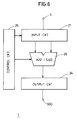
- Output circuit 24 does not have to have a selecting function in the configuration of Fig. 6.
- Output circuit 24 is required to have a function of buffering and latching (in the case of a clock synchronizing operation) an output of arithmetic unit 26.
- the circuit scale is reduced.
- Such configuration may be employed that intermediate data w k is output after all intermediate data z k are output from preprocessing section 1.
- Fig. 7A shows configuration of data rearranging circuit 2 of Fig. 1.
- Data rearranging circuit 2 includes an input circuit 31 for receiving intermediate data from a terminal 500, a shift register 32 for sequentially storing therein data from input circuit 31, and a selector 33 for sequentially reading four intermediate data stored in shift register 32 from the least significant bit.
- input circuit 31 After alternately receiving intermediate data z k and intermediate data w k and outputting all of intermediate data z k in advance, input circuit 31 sequentially outputs intermediate data w k .
- This configuration can easily be implemented by using a register for storing intermediate data w k therein.
- input circuit 31 sequentially inputs intermediate data from terminal 500.
- Input circuit 31 has a function of latching intermediate data w k until the reading of intermediate data z k by the selector is completed.
- a data acceptation, latching and output operation of input circuit 31 is controlled by a control circuit 34.
- Shift register 32 stores therein four intermediate data from input circuit 31.
- Shift register 32 includes four 8-bit registers 32a-32d in a row direction as shown in Fig. 7B.
- Fig. 7B shows a state where four intermediate data z 1 to z 4 are stored in shift register 32.
- Intermediate data z k from input circuit 31 are sequentially stored in registers 32a - 32d. After all intermediate data z1 to z4 are stored in register 32, data of registers 32a - 32d are read in parallel sequentially from the respective least significant bits.
- Such configuration can be implemented by shift registers capable of shifting in both row and column directions. Even by use of a shift register capable of shifting only in the row direction, if a register stage is selected by selector 33, the data rearranging operation can be realized.
- a data bit shifting operation of shift register 32 is controlled by control circuit 34.
- Selector 33 reads data of 4 bits in parallel from shift register 32 under control by control circuit 34.
- Four-bit data z kn are output from a terminal 501 in the configuration of Fig. 7A.
- Fig. 8 shows configuration of product sum operation circuit 6.
- product sum operation circuit 6 includes a partial sum generating circuit 41 for generating a partial sum in accordance with data from terminal 501, and an accumulator 42 for accumulating an output of partial sum generating circuit 41.
- Partial sum generating circuit 41 includes an ROM (Read Only Memory) 43 for receiving 4-bit data z kn and as an address signal.
- ROM 43 stores the partial sum shown in, for example, equation (10) in the form of table and, when supplied with 4-bit data z kn , ROM 43 outputs a corresponding value.
- Accumulator 42 includes an adder 44 for receiving a partial sum from partial sum generating circuit 41 at its one input, an accumulating register 45 for storing an output of adder 44, and a shifter 46 for shifting an output of register 45 by predetermined bits to apply the shifted output to the other input of adder 44.
- Output data yj is applied from shifter 46 to terminal 5.
- control circuit 47 The operation of partial sum generating circuit 41 and accumulator 42 is carried out by control circuit 47.
- Fig. 9 shows another configuration of a product sum operation circuit.
- the product sum operation circuit shown in Fig. 9 is different from the configuration shown in Fig. 8 in that a partial sum generating circuit 41 includes two ROMs 43a and 43b and an adder 48 for adding outputs of ROMs 43a and 43b.
- ROM 43a receives higher order bitS; while ROM 43b receives lower order bits.
- partial sums P and Q shown in the following equations are made by ROMs 43a and 43b.
- the number of words to be stored into the ROMs is drastically reduced. This is because the number of words to be stored is determined by the number of bits of an address signal and increased in proportion to two's power of the bit number.
- product sum operation section 3 includes eight product sum operation circuits 6a - 6h. Intermediate data z k and w k are not calculated simultaneously. When intermediate data w k are calculated after all intermediate data z k are calculated and then output data y0, y2, y4 and y6 are calculated, product sum operation section 3 can be formed of four product sum operation circuits 6a - 6d as shown in Fig. 10.
- Product sum operation circuits 6a - 6d calculate y0 and y1, y2 and y3, y4 and y5, and y6 and 7, respectively.
- the contents of an ROM for partial sum generation is changed in accordance with intermediate data z k and w k . If the ROM is structured in bank architecture, the change of the coefficient table can easily be realized.
- an 8-point one-dimensional IDCT processor includes a data rearranging circuit 2 for rearranging data from an input terminal 4, a product sum operation section 3 for performing a production sum operation in accordance with an output of data rearranging circuit 2, and a postprocessing section 7 for carrying out addition and subtraction of a predetermined combination of outputs of product sum operation section 3.
- Data rearranging circuit 2 and postprocessing section 7 are of the same configurations as those of rearranging circuit 2 and preprocessing section 1 of Fig. 4, respectively. An operation will now be described.
- the relationship between data yj and xi is represented in the following matrix form (12).
- A 1 2 cos ⁇ 4
- B 1 2 cos ⁇ 8
- C 1 2 sin ⁇ 8
- D 1 2 cos ⁇ 16
- E 1 2 cos 3 ⁇ 16
- F 1 2 sin 3 ⁇ 16
- G 1 2 sin ⁇ 16
- This coefficient matrix is a transposed matrix of the coefficient matrix of equation (5). If the symmetry with respect to rows of the coefficient matrix of expression (12) is utilized, expression (12) is changed to the following equivalent expression (13).
- the processor shown in Fig. 11 carries out an IDCT operation in accordance with expression (13).
- M2 (A ⁇ y0 - C ⁇ y2 - A ⁇ y4 + B ⁇ y6) for x2.
- the bit data is subjected to a product sum operation in product sum operation section 3. Accordingly, the remaining terms are obtained.
- an intermediate term N2 (F ⁇ y1 - D ⁇ y3 + G ⁇ y6 + E ⁇ y7) for x2 is obtained.
- Data rearranging circuit 2 may alternately output data bits (y0, y2, y4, y6) and data bits (y1, y3, y5, y7).
- Postprocessing section 7 has the same configuration as that of Fig. 5 or 6.
- the order in which data are selected in the input circuit is made by control circuit 25.
- data may be applied in the order of x0, x7, x1, x6, x2, x5, x3, x4 to output circuit 24, and output circuit 24 may output the data in the order of x0, x1, ... x7.
- the processor includes a preprocessing section 1, a data rearranging circuit 2, a product sum operation section 3, a postprocessing section 7 and a control circuit 8.
- Preprocessing section 1 has its input connected to an input terminal 4 and its output connected to data rearranging circuit 2.
- Data rearranging circuit 2 has its output connected to product sum operation section 3.
- Product sum operation section 3 has its output connected to an input of postprocessing section 7. The output of postprocessing section 7 is supplied through an output terminal 5.
- Product sum operation section 3 includes first to eighth product sum operation circuits 6a - 6h.
- Control circuit 8 switches DCT operation and IDCT operation and also controls the operation of the respective circuits.
- inverse DCT processing data passes intactly through preprocessing section 1, whereby the processor functions equally to the inverse DCT processor shown in Fig. 11 as follows. That is, the data input from input terminal 4 passes intactly through preprocessing section 1 and then rearranged in data rearranging circuit 2. The rearranged data is transmitted in turn from lower order bits to the product sum operation section. The data subjected to the product sum operation in the product sum operation section is transmitted to postprocessing section 7 and then subjected to addition/subtraction for calculating output data. The added/subtracted data is output from output terminal 5.
- Control circuit 1 Changes in coefficients in product sum operation section 3 are made by control circuit 1. This is easily realized by switching of banks of ROM or the like.
- the above-described processor performs a one-dimensional DCT or IDCT operation.
- This processor can be developed to be able to perform a two-dimensional DCT or IDCT operation.
- Fig. 13 shows configuration of a two-dimensional DCT processor according to the present invention.
- the two-dimensional DCT processor includes a first one-dimensional DCT processing section 11a, a second one-dimensional DCT processing section 11b and a transposition circuit 12.
- one-dimensional DCT processing section 11a carries out DCT processing with respect to rows, while second one-dimensional DCT processing section 11b carries out DCT processing with respect to columns.
- Transposition circuit 12 outputs in the order of columns the data applied in the order of rows.
- First and second processing sections 11a and 11b have the same configuration as that of the one-dimensional DCT processor shown in Fig. 1 and include a preprocessing section 1 (1a, 1b), a data rearranging circuit 2 (2a, 2b) and a product sum operation section 3 (3a, 3b).
- a preprocessing section 1 (1a, 1b) a data rearranging circuit 2 (2a, 2b)
- product sum operation section 3 3a, 3b
- Preprocessing section 1a carries out preprocessing for the respective row vector data. For a zeroth row, for example, data (x00 ⁇ x07), (x01 ⁇ x06), (x02 ⁇ x05) and (x03 ⁇ x04) are output from preprocessing section 1a.
- Data rearranging circuit 2a rearranges four words (four addition data or four subtraction data) to output the rearranged data to product sum operation section 3a.
- Product sum operation section 3a applies a product sum operation to the applied data.
- the processing operation of data rearranging circuit 2a and product sum operation section 3a is the same as those of the processor shown in Fig. 4.
- first one-dimensional DCT processing section 11a outputs in the order of rows 8-term row vector data Rk subjected to one-dimensional DCT processing with respect to a row direction.
- This intermediate data Rk is applied to transposition circuit 12 and stored therein in the order of rows.
- transposition circuit 12 When 8-row intermediate data R0 - R7 are stored in transposition circuit 12, transposition circuit 12 outputs intermediate data in the order of columns to second one-dimensional DCT processing circuit 11b.
- the intermediate data stored in transposition circuit 12 is data which is subjected to an operation processing with respect to "i" in expression (14).
- Transposition circuit 12 outputs intermediate data in the order of columns. In the zeroth column, for example, data R00, R10, R20, ... R70 are read in turn.
- Second one-dimensional DCT processing section 11b carries out the same preprocessing, the same data rearranging processing and the same product sum operation processing for each column as those of first one-dimensional DCT processing section 11a. Accordingly, second one-dimensional DCT processing section 11b outputs data subjected to addition with respect to "j" in expression (14). That is, 8-term column vector data are output in the order of columns from output terminal 5.
- the data appearing on output terminal 5 are data subjected to one-dimensional DCT processing in both row and column directions, i.e., two-dimensional DCT processing.
- transformation from rows to columns in transposition circuit 12 is realized by changing an address of a buffer memory in the row direction in data writing and in the column direction in data reading.
- the two-dimensional IDCT processing can be realized by expanding the one-dimensional IDCT processor shown in Fig. 11.
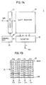
- Fig. 14 shows configuration of a two-dimensional IDCT processor.
- the two-dimensional IDCT processor includes a first one-dimensional IDCT processor 13a and a second one-dimensional IDCT processor 13b.
- one-dimensional IDCT processor 13a includes a data rearranging circuit 2a, a product sum operation section 3a and a postprocessing section 7a.
- Second one-dimensional IDCT processor 13b includes a data rearranging circuit 2b, a product sum operation section 3b and a postprocessing section 7b. Both first and second one-dimensional IDCT processors 13b and 13b carry out the same processing as that of the one-dimensional IDCT processor shown in Fig. 11.
- Input terminal 4 is supplied with input data in the order of rows.
- First IDCT processor 13a carries out an IDCT processing with respect to rows.
- Transposition circuit 12 sequentially stores therein intermediate data applied in the order of rows from first IDCT processor 13a and outputs the stored intermediate data in the order of columns.
- Second IDCT processor 13b carries out an IDCT processing for the respective columns. Accordingly, output terminal 5 is supplied with the data subjected to the IDCT processing in both row and column directions, i.e., two-dimensional IDCT processing, in the order of columns.
- Fig. 15 shows configuration of a two-dimensional DCT/IDCT processor being still another embodiment of the present invention.
- the processor of Fig. 15 includes a first one-dimensional DCT/IDCT processor 14a, a second one-dimensional DCT/IDCT processor 14b, and a transposition circuit 12 provided between processors 14a and 14b.
- First and second processors 14a and 14b are of the same configuration as that of the processor shown in Fig. 12 and include a preprocessing section 1 (1a, 1b), a data rearranging circuit 2 (2a, 2b), a product sum operation section 3 (3a, 3b) and a postprocessing section 7 (7a, 7b).
- FIG. 15 An operation of the processor of Fig. 15 is identical to those of the processors of Figs. 13 and 14.
- One processing mode of the DCT processing and the IDCT processing is set by a control circuit not shown (corresponding to control circuit 8 of Fig. 12).
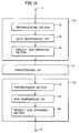
- Fig. 16 shows an example of use of a DCT processor which is incorporated integrally on one semiconductor substrate simultaneously with other functional circuitry.
- a semiconductor integrated circuit (semiconductor chip) 50 includes a DCT processor 51 and functional circuits 52, 53 and 54.
- DCT processor 51 has such configuration as shown in Fig. 13 or 14.
- Functional circuits 52, 53 and 54 have different functions A, B and C, respectively.
- functions A, B and C include such functions necessary for image compression as quantization, variable length coding (entropy coding) and the like.
- the functions necessary for image compression are standardized by, for example, JPEG (Joint of Photographic Expert Group).
- DCT processor 51 is used in cooperation with (or in clock synchronization with) functional circuits 52, 53 and 54.
- the functional circuits integrated together with the DCT processor are dedicated circuits having specific functions.
- the functional circuits are not limited to such dedicated circuits and may be integrated together with a microprocessor or a programmable functional block 56 such as a DSP (Digital Signal Processor) as shown in, for example, Fig. 17.
- the DCT processor may be integrated together with a dedicated functional circuit 55 and programmable functional block 56 in combination as shown in Fig. 17.
Description
- The present invention relates generally to data processors and data processing methods and, more particularly, to an apparatus and method for carrying out discrete cosine transform or inverse cosine transform of data.
- In order to process video data at a high speed, high effective coding is carried out. In high effective coding, a data amount of a digital video signal is compressed with picture quality being maintained as high as possible. In high effective coding, a redundant component of the signal is first removed for efficient coding. For this purpose, orthogonal transform techniques are often employed. As one of the orthogonal transform techniques, discrete cosine transform DCT is provided. The DCT is implemented by a simple product sum operation using a cosine function as a coefficient. The DCT is defined by the following expression (1):

- The expression (1) represents a case where input data X is of N terms. 2m points are generally employed, where m is a natural number. A description will now be made on 8 point DCT where N = 8 (m = 3). As can be seen from the expression (1), DCT is a matrix operation, and in practice, this processing is realized by product sum operation.
- Fig. 1 shows configuration of a conventional DCT processor. This DCT processor is described in, for example, IEEE, Proceedings of Custom Integrated Circuits Conference 89, 1989, pp. 24.4.1 to 24.4.4.
- Referring to Fig. 1, the conventional DCT processor includes eight sum product operation units 100a to 100h arranged in parallel for calculating respective terms y0 to y7 of output data Y.
- Each of product sum operation units 100a to 100h is of the same configuration and includes a parallel multiplier 101 for taking a product of input data xi (i = 0 to 7) and a predetermined weighting coefficient, and an accumulator 102 for accumulating an output of parallel multiplier 101 to generate output data yj (j = 0 to 7). Here, reference characters 101 and 102 generically denote respective components 101a to 101h and 102a to 102h. In the following description also, reference numerals having no suffixes generically denote corresponding elements.
- Accumulator 102 includes a 2-input adder 103 for receiving an output of parallel multiplier 101 at its one input, and an accumulating register 104 for latching an output of adder 103. An output of register 104 is applied to an output terminal 106 and also to the other input of adder 103. Data yj of the respective terms of output data Y are sequentially output through a selector not shown from output terminal 106. An operation will now be described.
- Identical data are applied through an input terminal 105 to product sum operation units 100a to 100h. The following arithmetic operation is carried in each of product sum operation units 100a - 100h:
For example, data y0 of a zeroth term in an output data vector Y is calculated as follows in product sum operation unit 100a. - When receiving zeroth-term data x0 (hereinafter referred to simply as input data) in an input data vector, parallel multiplier 101a outputs a product A (0, 0)·x0 of data x0 and a coefficient A (0, 0) to adder 103a. Register 104a is being reset, and the content thereof is 0. Accordingly, product A (0, 0)·x0 is output from adder 103a and then stored in register 104a.
- When input data x1 is applied, a product A (1, 0)·x1 is output from multiplier 101a. An output of adder 103a is
- By repetition of such an operation, an output of accumulator 102a provided after application of input data x7 isA (i, 0) · xi, so that output data y0 is obtained. Similar calculation (which differs merely in values of a weighting coefficient A (i, j)) is carried out also in the remaining product sum operation units 100b - 100h, and output data y1 - y7 are obtained. These output data y0 - y7 are sequentially output through output terminal 106.

- In contrast to the DCT operation, there is an inverse DCT operation for carrying out the inverse operation of the DCT operation. The inverse DCT (IDCT) is expressed as follows:
- In other words, the DCT and the IDCT can be carried out on the same hardware. An increase in hardware is only concerned with a control circuit (not shown) for making a selection between a coefficient for DCT and that for IDCT.
- The above-described one-dimensional DCT operation can be expanded to a two-dimensional DCT operation. The two-dimensional DCT operation is obtained by making both input data vector X and output data vector Y be two-dimensional vectors.
- Fig. 2 shows configuration of a conventional two-dimensional DCT (or IDCT) processor. Referring to Fig. 2, the processor includes a first one-dimensional DCT processing section 111a for subjecting input data from input terminal 105 to one-dimensional DCT processing, a transposition circuit 112 for rearranging rows and columns of an output of first one-dimensional DCT processing section 111a, and a second one-dimensional DCT processing section 111b for subjecting an output of transposition circuit 112 to one-dimensional DCT processing. First one-dimensional DCT processing section 111a performs a DCT (or IDCT) operation in a row direction, and second one-dimensional DCT processing section 111b performs a DCT (or IDCT) operation in a column direction.
- Fig. 3 is a diagram showing configuration of the transposition circuit of Fig. 2. Referring to Fig. 3, transposition circuit 112 includes a buffer memory 121 and an address generation circuit 122 for generating write/read addresses of buffer memory 121. Buffer memory 121 receives output data of first-one-dimensional DCT processing section 111a through an input terminal 125 and sequentially stores the same therein in accordance with an address signal from address generation circuit 122. Also, buffer memory 121 applies corresponding data from an output terminal 126 to second one-dimensional DCT processing section 111b in accordance with an address signal from address generation circuit 122. An operation will now be described. Input data X and output data Y are two dimensional, the elements of which are each represented by x (i, j) and y (i, j), i, j = 0, 1 ... 7.
- Input data are applied in the order of rows to first one-dimensional DCT processing section 111a. More specifically, input data are applied to input terminal 105 in the order of 8-term row vectors x (0, j), x (1, j), ... x (7, j).
- First one-dimensional DCT processing section 111a performs the DCT operation for each row vector to output intermediate data Z. At that time, first DCT processing section 111a outputs intermediate data of row vectors in the order of rows, i.e., z (0, j), z (1, j) .... Accordingly, a DCT operation in the row direction of input data X is carried out.
- As shown in Fig. 3, transposition circuit 112 first stores the intermediate data from first DCT processing section 111a into buffer memory 121 in the order of receiving of the intermediate data (the order of rows).
- Then, intermediate data Z are read in the order of columns, i.e., the order of column vectors z (i, 0), z (i, 1) ... from buffer memory 121.
- Intermediate data Z read in the order of columns are applied to second DCT processing section 111b. Second DCT processing section 111b carries out on the intermediate data one-dimensional DCT processing. Accordingly, data subjected to one-dimensional DCT processing in the column direction are output from second one-dimensional DCT processing section 111b. Output data Y from second one-dimensional DCT processing section 111b are output in the order of columns from output terminal 106. As a result, two-dimensional DCT shown by the following equation (3) is performed.

- First and second DCT processing sections 111a and 111b carry out the same processing except for coefficients in the parallel multiplying circuits. If multiplication coefficients of first and second DCT processing sections 111a and 111b are changed, two-dimensional IDCT shown by the following equation (4) is carried out.
- The DCT processing and IDCT processing as shown above include a product sum operation. A product operation of this product sum operation is carried out by the parallel multipliers shown in Fig. 1. A multiplier in general requires a large number of adders and the like and has a large scale. Thus, there is a disadvantage that a conventional DCT processor requiring a plurality of parallel multipliers is not allowed to be sized-down.
- In a semiconductor integrated circuit for carrying out a synchronization operation, the upper limit of operation speed is determined by a worst delay path (the path which provides a maximum delay). In the conventional configuration, the worst delay path is established by a parallel multiplier, and the operation speed depends on processing speed of the parallel multiplier. It is thus difficult to implement a fast DCT processing and a fast IDCT processing.
- From International Journal of Electronics, vol. 69, no. 2, August 1990, London, pages 233 - 246; K.W. Current et al.: "Unified forward and inverse discrete cosine transform architecture and proposed VLSI implementation" a processor and a method for selectively carrying out one-dimensional discrete cosine transform and inverse discrete cosine transform are known. The processor comprises a preshuffle, a butterfly, a multiplier, a pre/postprocessor, a scalar and a postshuffle. The processor performs the product sum operations using the parallel operational units (butterfly and hardware multipliers). For DCT, post-processing is required, whilst for IDCT pre-processing is required.
- From Tencon '89, 22 - 24 November 1989, India, pages 74 - 77; S.N. Merchant et al.: "Distributed Arithmetic Architecture for Image Coding" a discrete cosine transform processor is known performing a two-dimensional discrete cosine transform by column conversion following the row conversion.
- From 1989 IEEE Symposium on Circuits and Systems, 8/11 May 1989, Portland, Oregon, vol. 1, pages 220 - 225; V. Rampa et al.: "Computer-Aided Synthesis of a Bi-Dimensional Discrete Cosine Transform Chip" a discrete cosine transform processor is known for carrying out bi-dimensional discrete cosine transform, wherein a serial multiplier and accumulator performs the matrix operation using a look-up table.
- It is the object of the present invention to provide a down-sized data processor which operates at high speed for carrying out at least one of discrete cosine transform and inverse discrete cosine transform.
- This object is solved by a processor with the features of claim 1 or 12 and by a method having the features of claims 21 or 22.
- Preferred developments of the processor and the method are given in the respective subclaims.
- Since the number of times of multiplication is reduced and no parallel multipliers are employed, the DCT operation and IDCT operation are carried out at a high speed with fewer circuit components.
- The foregoing and other objects, features, aspects and advantages of the present invention will become more apparent from the following detailed description of the present invention when taken in conjunction with the accompanying drawings.
- Fig. 1 is a diagram showing configuration of a conventional one-dimensional DCT processor.
- Fig. 2 is a diagram showing configuration of a conventional two-dimensional DCT processor.
- Fig. 3 is a diagram showing configuration of a transposition circuit of Fig. 2.
- Fig. 4 is a diagram showing configuration of a one-dimensional DCT processor being one embodiment of the present invention.
- Fig. 5 is a diagram showing an example of configuration of a preprocessing section shown in Fig. 4.
- Fig. 6 is a diagram showing an example of modification of the preprocessing section of Fig. 5.
- Fig. 7A is a diagram showing an example of configuration of a data rearranging circuit of Fig. 4.
- Fig. 7B is a diagram showing the contents of a shift register of Fig. 7A.
- Fig. 8 is a diagram showing an example of configuration of a product sum operation circuit of Fig. 4.
- Fig. 9 is a diagram of an example of modification of the product sum operation circuit of Fig. 8.
- Fig. 10 is a diagram showing an example of modification of the one-dimensional DCT processor of Fig. 1.
- Fig. 11 is a diagram showing-configuration of a one-dimensional IDCT processor being another embodiment of the present invention.
- Fig. 12 is a diagram showing configuration of a one-dimensional DCT/IDCT processor being still another embodiment of the present invention.
- Fig. 13 is a diagram showing configuration of a two-dimensional DCT processor being still another embodiment of the present invention.
- Fig. 14 is a diagram showing configuration of a two-dimensional IDCT processor being still another embodiment of the present invention.
- Fig. 15 is a diagram showing configuration of a two-dimensional DCT/IDCT processor being still another embodiment of the present invention.
- Fig. 16 is a diagram showing configuration of a semiconductor integrated circuit apparatus including the DCT processor of the present invention.
- Fig. 17 is a diagram showing an example of modification of the semiconductor integrated circuit of Fig. 16.
-
- Fig. 4 schematically shows configuration of a one-dimensional DCT processor being one embodiment of the present invention.
- Referring to Fig. 4, the processor includes a preprocessing section 1 for receiving input data xi from an input terminal 4 to preprocess the received input data xi on the basis of characteristics inherent to DCT operation, a data rearranging circuit 2 for rearranging data output from preprocessing section 1, and a product sum operation section 3 for carrying out a product sum operation on data from data rearranging circuit 2.
- This processor carries out an eight-point DCT operation. Thus, product sum operation section 3 includes eight product sum operation circuits 6a - 6h. Respective product sum operation circuits 6a - 6h provide respective output data y0, y2, y4, y6, y1, y3, y5 and y7 to sequentially apply the output data to an output terminal 5, (the sequential application unit is not shown in the figure).
- A description will now be made on the principle of an 8-point one-dimensional DCT processing operation of the present invention before a detailed description of configuration of each section. If the relationship between input data xi (i = 0, 1, ... 7) and output data yj (j = 0, 1, ... 7) shown in equations (1) and (2) is expressed in a matrix form, the following representation (5) is obtained:where

- In derivation of the above relation (5), the well-known known characteristics of trigonometric function such as
- In the above relation (5), a coefficient matrix is horizontally symmetrical with respect to columns. By use of this symmetry, relation (5) can be transformed to the following representation (6):
- If a comparison is made between the above relations (5) and (6), it is apparent that the number of times of multiplication for acquiring output data yj is reduced to a half in relation (6) as compared to relation (5). DCT processing in accordance with relation (6) is carried out in this embodiment.
- With reference to Fig. 4, preprocessing section 1 generates the following eight intermediate data from input data xi sequentially applied from input terminal 4 by selectively carrying out addition or subtraction. The intermediate data are:
- The result of preprocessing from preprocessing section 1 is represented in finite word length. In the following description, it is assumed that the preprocessing result is indicated by 8-bit data in two's complement notation.
- In order to calculate output data yj by using the preprocessed data from preprocessing section 1, the matrix operation of relation (6) is carried out.
- With respect to output data y2, for example, the following relation (7) is carried out:
- Data rearranging circuit 2 of Fig. 4 receives preprocessing results zk (k = 1, ... 4) from preprocessing section 1. When receiving four necessary preprocessing results zk, data rearranging circuit 2 outputs the least significant bits of respective four preprocessing results zk in parallel to product sum operation section 3. The parallel bit output is carried out sequentially in bit figure until the most significant bit is output.
- Product sum operation circuit 6b for output data y2 carries out an operation in accordance with a relation (8) which is a further equivalent transformation of relation (7).
- 4-bit data z1n, z2n, z3n,and z4n are applied in parallel to product sum operation circuit 6b for data y2. The values of coefficients B1, B2, B3 and B4 can be calculated in advance. Product sum operation circuit 6b stores therein a partial sum (10) shown below in the form of a ROM table and outputs a corresponding partial sum with 4-bit data z1n, z2n, z3n and z4n used as an address.
- Referring to Fig. 4, in product sum operation section 3, product sum operation circuits 6a - 6d apply the operation to the same data zk in parallel to produce output data y0, y2, y4 and y6. Product sum operation circuits 6e - 6h apply the operation to the same data wk in parallel to produce output data y1, y3, y5 and y7.
- Output data y0 to y7 are sequentially output in this order from output terminal 5 by a selector not shown. A description will now be given on a detailed configuration of each section shown in Fig. 4.
- Fig. 5 shows configuration of preprocessing section 1 shown in Fig. 4. Preprocessing section 1 includes an input circuit 21 for receiving input data xi sequentially applied from input terminal 4. Input circuit 21 outputs input data xp and xq in a predetermined combination under control by a control circuit 25. Here, a relation
- Preprocessing section 1 further includes a 2-input adder 22 for adding outputs of input circuit 21, a subtractor 23 for subtracting outputs of input circuit 21, and an output circuit 24 for selecting one of respective outputs of adder 22 and subtractor 23 under control by control circuit 25. Adder 22 and subtractor 23 carry out addition and subtraction for the applied data under control by control circuit 25.
- Output circuit 24 preferably alternately selects the output of adder 22 and that of subtractor 23. An operation will now be described.
- Input circuit 21 receives input data X to sequentially output sets of data (x0, x7), (x1, x6), (x2, x5), and (x3, x4).
- Adder 22 adds the data of each set. Adder 22 sequentially outputs data zk, i.e., (x0 + x7), (x1 + x6), (x2 + x5) and (x3 + x4).
- Subtractor 23 sequentially outputs data wk, i.e., (x0 - x7), (x1 - x6), (x2 - x5) and (x3 - x4).
- Output circuit 24 alternately outputs data zk and data wk.
- Parallel multiplication circuits 6a to 6d of Fig. 1 carry out an operation in accordance with data zk, while parallel multiplication circuits 6e to 6h carry out an operation in accordance with data wk.
- Output circuit 24 alternately outputs addition data zk and subtraction data wk. This makes it possible to produce output data y0 to y7 in this order from product sum operation section 3 and implement a pipelined architecture for processing data in synchronization with a clock signal.
- In that case, it is unnecessary that adder 22 and subtractor 23 carry out an arithmetic operation simultaneously. Accordingly, as shown in Fig. 6, an arithmetic unit 26 for alternately performing the adding processing and the subtracting processing under control by control circuit 25 may be employed. Output circuit 24 does not have to have a selecting function in the configuration of Fig. 6. Output circuit 24 is required to have a function of buffering and latching (in the case of a clock synchronizing operation) an output of arithmetic unit 26. In the configuration of Fig. 6, since the addition and subtraction are carried out in a single arithmetic unit 26, the circuit scale is reduced.
- Such configuration may be employed that intermediate data wk is output after all intermediate data zk are output from preprocessing section 1.
- Fig. 7A shows configuration of data rearranging circuit 2 of Fig. 1. Data rearranging circuit 2 includes an input circuit 31 for receiving intermediate data from a terminal 500, a shift register 32 for sequentially storing therein data from input circuit 31, and a selector 33 for sequentially reading four intermediate data stored in shift register 32 from the least significant bit.
- After alternately receiving intermediate data zk and intermediate data wk and outputting all of intermediate data zk in advance, input circuit 31 sequentially outputs intermediate data wk. This configuration can easily be implemented by using a register for storing intermediate data wk therein.
- When intermediate data wk are applied after all of intermediate data zk are applied, input circuit 31 sequentially inputs intermediate data from terminal 500. Input circuit 31, however, has a function of latching intermediate data wk until the reading of intermediate data zk by the selector is completed. A data acceptation, latching and output operation of input circuit 31 is controlled by a control circuit 34.
- Shift register 32 stores therein four intermediate data from input circuit 31. Shift register 32 includes four 8-bit registers 32a-32d in a row direction as shown in Fig. 7B. Fig. 7B shows a state where four intermediate data z1 to z4 are stored in shift register 32.
- Intermediate data zk from input circuit 31 are sequentially stored in registers 32a - 32d. After all intermediate data z1 to z4 are stored in register 32, data of registers 32a - 32d are read in parallel sequentially from the respective least significant bits. Such configuration can be implemented by shift registers capable of shifting in both row and column directions. Even by use of a shift register capable of shifting only in the row direction, if a register stage is selected by selector 33, the data rearranging operation can be realized.
- A data bit shifting operation of shift register 32 is controlled by control circuit 34. Selector 33 reads data of 4 bits in parallel from shift register 32 under control by control circuit 34.
- Four-bit data zkn are output from a terminal 501 in the configuration of Fig. 7A.
- Fig. 8 shows configuration of product sum operation circuit 6. Referring to Fig. 8, product sum operation circuit 6 includes a partial sum generating circuit 41 for generating a partial sum in accordance with data from terminal 501, and an accumulator 42 for accumulating an output of partial sum generating circuit 41.
- Partial sum generating circuit 41 includes an ROM (Read Only Memory) 43 for receiving 4-bit data zkn and as an address signal. ROM 43 stores the partial sum shown in, for example, equation (10) in the form of table and, when supplied with 4-bit data zkn, ROM 43 outputs a corresponding value. By constructing this partial sum generating circuit 41 in the form of the ROM table, a partial sum can be generated at a high speed without any multiplication.
- Accumulator 42 includes an adder 44 for receiving a partial sum from partial sum generating circuit 41 at its one input, an accumulating register 45 for storing an output of adder 44, and a shifter 46 for shifting an output of register 45 by predetermined bits to apply the shifted output to the other input of adder 44. Output data yj is applied from shifter 46 to terminal 5. A description will now be made on an operation thereof, taking output data y2 as an example.
- Four-bit data zkn are applied in turn from the least significant bit to product sum generating circuit 41. Product sum generating circuit 41 sequentially outputs a partial sum
- First, a partial sum
- Then, a partial sum
- Shifter 46 shifts the contents of register 45 by one bit. Accordingly, an output of shifter 46 is shown as below:
- The output of adder 44 is shown as below:
- If data zk0 is applied, the contents of register 45 is the value shown in relation (8) since the data represented by the above relation (11) is shifted by one bit and then added by adder 44. After that, the shifting operation by shifter 46 is stopped and the contents of register 45 is read, whereby output data y2 is obtained.
- The operation of partial sum generating circuit 41 and accumulator 42 is carried out by control circuit 47.
- Fig. 9 shows another configuration of a product sum operation circuit. The product sum operation circuit shown in Fig. 9 is different from the configuration shown in Fig. 8 in that a partial sum generating circuit 41 includes two ROMs 43a and 43b and an adder 48 for adding outputs of ROMs 43a and 43b.
- ROM 43a receives higher order bitS; while ROM 43b receives lower order bits. In this configuration, partial sums P and Q shown in the following equations are made by ROMs 43a and 43b.
- In the above configuration, product sum operation section 3 includes eight product sum operation circuits 6a - 6h. Intermediate data zk and wk are not calculated simultaneously. When intermediate data wk are calculated after all intermediate data zk are calculated and then output data y0, y2, y4 and y6 are calculated, product sum operation section 3 can be formed of four product sum operation circuits 6a - 6d as shown in Fig. 10.
- Product sum operation circuits 6a - 6d calculate y0 and y1, y2 and y3, y4 and y5, and y6 and 7, respectively. The contents of an ROM for partial sum generation is changed in accordance with intermediate data zk and wk. If the ROM is structured in bank architecture, the change of the coefficient table can easily be realized.
- A description will now be made on a structure for an IDCT operation with reference to Fig. 11. Referring to Fig. 11, an 8-point one-dimensional IDCT processor includes a data rearranging circuit 2 for rearranging data from an input terminal 4, a product sum operation section 3 for performing a production sum operation in accordance with an output of data rearranging circuit 2, and a postprocessing section 7 for carrying out addition and subtraction of a predetermined combination of outputs of product sum operation section 3.
- Data rearranging circuit 2 and postprocessing section 7 are of the same configurations as those of rearranging circuit 2 and preprocessing section 1 of Fig. 4, respectively. An operation will now be described.
- Input data yj (j = 0, 1, ... 7) applied to terminal 4 undergoes an IDCT processing, so that output data xi (i = 0, 1, ... 7) is transmitted to terminal 5. The relationship between data yj and xi is represented in the following matrix form (12).where

- Data rearranging circuit 2 receives data yj (j = 0, 1, ... 7) from terminal 4 to rearrange data y0, y2, y4 and y6 and sequentially output the rearranged data from the least significant bit. That is, 4-bit data Y0n, y2n, y4n and Y6n (n = 0, 1, ... 7) of input data yj are output from data rearranging circuit 2, so that generation and accumulation of partial sums are carried out. As intermediate data, the following data is output:
- Data rearranging circuit 2 may alternately output data bits (y0, y2, y4, y6) and data bits (y1, y3, y5, y7). Each of product sum operation circuits 6a - 6d calculates
- Postprocessing section 7 obtains a sum of and a difference between intermediate data Mi and Ni to generate output data xi and output the same to terminal 5. Accordingly, the following relation is obtained:
- Postprocessing section 7 has the same configuration as that of Fig. 5 or 6. In that case, input circuit 21 sequentially or alternately receives intermediate terms Mi (i = 0 to 3), Ni (i = 0 to 3) to apply a desired combination of the terms to adder/subtractors 22, 23 (or 26). The order in which data are selected in the input circuit is made by control circuit 25. In this case, data may be applied in the order of x0, x7, x1, x6, x2, x5, x3, x4 to output circuit 24, and output circuit 24 may output the data in the order of x0, x1, ... x7.
- This one-dimensional IDCT processor can also be structured such that a single product sum operation circuit 6 calculates both intermediate terms Mi and Ni (i = 0 to 3).
- The product sum operation in DCT processing and that in IDCT processing are identical to each other except for their coefficient matrixes. Accordingly, as shown in Fig. 12, a processor capable of selectively performing the DCT processing and the IDCT processing is obtained.
- Referring to Fig. 12, the processor includes a preprocessing section 1, a data rearranging circuit 2, a product sum operation section 3, a postprocessing section 7 and a control circuit 8.
- Preprocessing section 1 has its input connected to an input terminal 4 and its output connected to data rearranging circuit 2. Data rearranging circuit 2 has its output connected to product sum operation section 3. Product sum operation section 3 has its output connected to an input of postprocessing section 7. The output of postprocessing section 7 is supplied through an output terminal 5. Product sum operation section 3 includes first to eighth product sum operation circuits 6a - 6h.
- Control circuit 8 switches DCT operation and IDCT operation and also controls the operation of the respective circuits.
- A description will now be made on an operation of the processor shown in Fig. 12. In the case of DCT processing, data is allowed to go intactly through postprocessing section 7. This causes the processor of Fig. 12 to function equally to the DCT processor shown in Fig. 4. That is, data input from input terminal 4 undergoes addition/subtraction in preprocessing section 1 and then rearranged in data rearranging circuit 2. The rearranged data is then transmitted in turn from lower order bits to the product sum operation section. The data subjected to a product sum operation shown in, for example, expression (5) in the product sum operation section passes through postprocessing section 7 and is then directly output from output terminal 5.
- In the case of inverse DCT processing, data passes intactly through preprocessing section 1, whereby the processor functions equally to the inverse DCT processor shown in Fig. 11 as follows. That is, the data input from input terminal 4 passes intactly through preprocessing section 1 and then rearranged in data rearranging circuit 2. The rearranged data is transmitted in turn from lower order bits to the product sum operation section. The data subjected to the product sum operation in the product sum operation section is transmitted to postprocessing section 7 and then subjected to addition/subtraction for calculating output data. The added/subtracted data is output from output terminal 5.
- Changes in coefficients in product sum operation section 3 are made by control circuit 1. This is easily realized by switching of banks of ROM or the like.
- The above-described processor performs a one-dimensional DCT or IDCT operation. This processor can be developed to be able to perform a two-dimensional DCT or IDCT operation.
- Fig. 13 shows configuration of a two-dimensional DCT processor according to the present invention. Referring to Fig. 13, the two-dimensional DCT processor includes a first one-dimensional DCT processing section 11a, a second one-dimensional DCT processing section 11b and a transposition circuit 12.
- First, one-dimensional DCT processing section 11a carries out DCT processing with respect to rows, while second one-dimensional DCT processing section 11b carries out DCT processing with respect to columns. Transposition circuit 12 outputs in the order of columns the data applied in the order of rows. First and second processing sections 11a and 11b have the same configuration as that of the one-dimensional DCT processor shown in Fig. 1 and include a preprocessing section 1 (1a, 1b), a data rearranging circuit 2 (2a, 2b) and a product sum operation section 3 (3a, 3b). A description will now be made on a two-dimensional DCT processing of 8 x 8 points taken as an example.
- If expression (3) is rewritten, the following expression (14) is obtained:
- Input terminal 4 is supplied with input data in the order of rows. That is, 8-term row vector data x(0, j), x(1, j) ... x (7, j) (j = 0, 1, ... 7) are applied in turn.
- Preprocessing section 1a carries out preprocessing for the respective row vector data. For a zeroth row, for example, data (x00 ± x07), (x01 ± x06), (x02 ± x05) and (x03 ± x04) are output from preprocessing section 1a. Data rearranging circuit 2a rearranges four words (four addition data or four subtraction data) to output the rearranged data to product sum operation section 3a. Product sum operation section 3a applies a product sum operation to the applied data. The processing operation of data rearranging circuit 2a and product sum operation section 3a is the same as those of the processor shown in Fig. 4.
- Accordingly, first one-dimensional DCT processing section 11a outputs in the order of rows 8-term row vector data Rk subjected to one-dimensional DCT processing with respect to a row direction. Rk is an 8-term row vector of
- This intermediate data Rk is applied to transposition circuit 12 and stored therein in the order of rows. When 8-row intermediate data R0 - R7 are stored in transposition circuit 12, transposition circuit 12 outputs intermediate data in the order of columns to second one-dimensional DCT processing circuit 11b. The intermediate data stored in transposition circuit 12 is data which is subjected to an operation processing with respect to "i" in expression (14). Transposition circuit 12 outputs intermediate data in the order of columns. In the zeroth column, for example, data R00, R10, R20, ... R70 are read in turn.
- Second one-dimensional DCT processing section 11b carries out the same preprocessing, the same data rearranging processing and the same product sum operation processing for each column as those of first one-dimensional DCT processing section 11a. Accordingly, second one-dimensional DCT processing section 11b outputs data subjected to addition with respect to "j" in expression (14). That is, 8-term column vector data are output in the order of columns from output terminal 5. The data appearing on output terminal 5 are data subjected to one-dimensional DCT processing in both row and column directions, i.e., two-dimensional DCT processing.
- Like the transposition in the circuit shown in Fig. 2, transformation from rows to columns in transposition circuit 12 is realized by changing an address of a buffer memory in the row direction in data writing and in the column direction in data reading.
- Also, the two-dimensional IDCT processing can be realized by expanding the one-dimensional IDCT processor shown in Fig. 11. Fig. 14 shows configuration of a two-dimensional IDCT processor.
- Referring to Fig. 14, the two-dimensional IDCT processor includes a first one-dimensional IDCT processor 13a and a second one-dimensional IDCT processor 13b.
- First, one-dimensional IDCT processor 13a includes a data rearranging circuit 2a, a product sum operation section 3a and a postprocessing section 7a. Second one-dimensional IDCT processor 13b includes a data rearranging circuit 2b, a product sum operation section 3b and a postprocessing section 7b. Both first and second one-dimensional IDCT processors 13b and 13b carry out the same processing as that of the one-dimensional IDCT processor shown in Fig. 11.
- Input terminal 4 is supplied with input data in the order of rows. First IDCT processor 13a carries out an IDCT processing with respect to rows.
- Transposition circuit 12 sequentially stores therein intermediate data applied in the order of rows from first IDCT processor 13a and outputs the stored intermediate data in the order of columns.
- Second IDCT processor 13b carries out an IDCT processing for the respective columns. Accordingly, output terminal 5 is supplied with the data subjected to the IDCT processing in both row and column directions, i.e., two-dimensional IDCT processing, in the order of columns.
- Fig. 15 shows configuration of a two-dimensional DCT/IDCT processor being still another embodiment of the present invention. The processor of Fig. 15 includes a first one-dimensional DCT/IDCT processor 14a, a second one-dimensional DCT/IDCT processor 14b, and a transposition circuit 12 provided between processors 14a and 14b.
- First and second processors 14a and 14b are of the same configuration as that of the processor shown in Fig. 12 and include a preprocessing section 1 (1a, 1b), a data rearranging circuit 2 (2a, 2b), a product sum operation section 3 (3a, 3b) and a postprocessing section 7 (7a, 7b).
- In the configuration of Fig. 15, like the configuration shown in Fig. 12, if preprocessing sections 1a and 1b and postprocessing sections 7a and 7b are selectively set in a through state and coefficients (used in the partial sum generation circuit) of product sum operation sections 3a and 3b are selected, then two-dimensional DCT and IDCT processings can selectively be carried out.
- An operation of the processor of Fig. 15 is identical to those of the processors of Figs. 13 and 14. One processing mode of the DCT processing and the IDCT processing is set by a control circuit not shown (corresponding to control circuit 8 of Fig. 12).
- Although the foregoing description has not been concerned with implementation forms of the DCT processors, the use of the above-described configuration makes it possible to easily incorporate all of DCT (inverse DCT) functions integrally on a semiconductor integrated circuit.
- It is also possible to incorporate all of the above-described DCT/inverse DCT functions integrally on a semiconductor integrated circuit and simultaneously incorporate functional circuitry having functions other than the DCT/inverse DCT functions integrally on one semiconductor substrate. Fig. 16 shows an example of use of a DCT processor which is incorporated integrally on one semiconductor substrate simultaneously with other functional circuitry.
- Referring to Fig. 16, a semiconductor integrated circuit (semiconductor chip) 50 includes a DCT processor 51 and functional circuits 52, 53 and 54.
- DCT processor 51 has such configuration as shown in Fig. 13 or 14. Functional circuits 52, 53 and 54 have different functions A, B and C, respectively. In application to video data processing, functions A, B and C include such functions necessary for image compression as quantization, variable length coding (entropy coding) and the like. The functions necessary for image compression are standardized by, for example, JPEG (Joint of Photographic Expert Group).
- In the configuration shown in Fig. 16, DCT processor 51 is used in cooperation with (or in clock synchronization with) functional circuits 52, 53 and 54.
- In the embodiment shown in Fig. 16, the functional circuits integrated together with the DCT processor are dedicated circuits having specific functions. The functional circuits are not limited to such dedicated circuits and may be integrated together with a microprocessor or a programmable functional block 56 such as a DSP (Digital Signal Processor) as shown in, for example, Fig. 17. Further, the DCT processor may be integrated together with a dedicated functional circuit 55 and programmable functional block 56 in combination as shown in Fig. 17.
- The summary of principal technical effects of the present invention is as follows:
- (i) Since the required number of times of multiplication is reduced by preprocessing in DCT processing or by postprocessing in IDCT processing, load on a product sum operation circuit is reduced.
- (ii) Since a product sum operation is carried out by a memory and an adder, the scale of circuitry is substantively reduced.
- (iii) Because of the above item (ii), a parallel multiplication circuit is unnecessary. Accordingly, when the entire processor performs a synchronizing operation, a higher operation speed on a worst delay path is easily achieved, facilitating a faster processing.
- (iv) Since the effect of the above item (iii) facilitates an upgrading of a DCT (or IDCT) processor, this effect is greatly advantageous particularly in implementation of the present DCT (or IDCT) processor on a semiconductor integrated circuit, together with the effect of reducing the circuit scale.
-
Claims (24)
- A processor having at least a function of carrying out one-dimensional discrete cosine transform DCT and one-dimensional inverse discrete cosine transform IDCT of N-term input data X, wherein said N is a positive integer, said processor comprising:preprocessing means (1; 1a, 1b) for carrying out addition and subtraction for each of sets of predetermined two terms of said input data X to generate a first set of addition data (zk) and a second set of subtraction data (wk) subject to DCT processing; andmatrix product means (2, 3; 2a, 3a; 2b, 3b) for obtaining a first matrix product of said first set of data (zk) from said preprocessing means (1, 1a, 1b) and a predetermined first coefficient matrix (B), and a second matrix product of said second set of data (wk) and a predetermined second coefficient matrix (B), whereinan output of said matrix product means provides N-term output data subjected to DCT processing,said matrix product means including table memory means (43) storing partial product sum data for respective outputs thereof at addresses provided by data received from said preprocessing means, andaccumulation means (42) for summing data received from said table memory means (43), said matrix product means performing N/2 point product sum operations,a postprocessing section (7; 7a, 7b) for receiving an output of said matrix product means to carry out addition and subtraction of predetermined 2-term data of the received N-term data and generate first and second sets (X2i, X2i + 1) of output data Yi, wherein the output of said postprocessing means providing N-term output data subject to IDCT processing, andcontrol means (8) for selectively enabling one of said preprocessing section (1; 1a, 1b) and said postprocessing section (7; 7a, 7b).
- The processor of claim 1, whereinsaid preprocessing means (1) includes:set generating means (21) for generating a set of pth term data X(p) and qth term data X(q) of said input data X1 whereaddition means (22; 26) for carrying out addition of 2-term data output from said set generating means (21); andsubtraction means (23, 26) for carrying out subtraction of the 2-term data output from said set generating means (21).
- The processor of claim 1 or 2, whereinsaid matrix product means (2, 3) includesstorage means (32) for sequentially receiving said first set of data from said preprocessing means (1) to store the received data therein, each of said first set of data having a plurality of bits, andparallel reading means (33) for reading, in parallel and in order, one-bit data in-the same bit figure of all of said first set of data stored in said storage means (32).
- The processor of one of claims 1 to 3, whereinsaid matrix product means (2, 3) includesstorage means (32) for sequentially receiving said second set of data from said preprocessing means (1) to store the received data therein, each of said second set of data having a plurality of bits, andparallel reading means (33) for reading in parallel and in order, one-bit data in the same bit figure of all of said second set of data stored in said storage means (32).
- The processor of claim 3 or 4, whereinsaid matrix product means (2, 3) further includesa plurality of first product sum operation means (6a - 6d), and wherein each said product sum operation means includes said table memory means (43) receiving parallel bit data from said parallel reading means (33) as an address signal to output a corresponding partial sum, said table memory means (43) storing in advance the product sum of a corresponding coefficient and said parallel bit data in a table form, andsaid accumulation means (42) accumulating outputs of said table memory means (43), said accumulation means (42)providing a first set of output data of said N-term output data.
- The processor of one of claims 1 to 5, whereinsaid matrix product means (2, 3) further includesa plurality of second product sum operation means (6e - 6h), and whereineach said second product sum operation means includes said table memory means (43) for receiving parallel bit data from said parallel reading means (33) as an address signal to output a corresponding partial sum, said table memory means (43) storing in advance a product sum of a corresponding coefficient and said parallel bit data in a table form, andsaid accumulation means (42) accumulating outputs of said table memory means (43) to generate a second set of data of said N-term output data.
- The processor of claim 5 or 6, whereinsaid accumulation means (42) includesaddition means (44) for receiving an output of said table memory means (43) at its one input,register means (45) for temporarily storing an output of said addition means (44), andshift means (46) for shifting storage data in said register means (45) by a bit to apply the shifted data to the other input of said addition means (44), a final output of said shift means providing said first or second set of data of said N-term output data.
- The processor of one of claims 1 to 7, whereinsaid postprocessing section (7) includes means (22, 23; 26) for carrying out addition and subtraction of (2i)th-term data Y (2i) and (2i + 1)th-term data Y (2i + 1) of N-term output data Y of said matrix product means (2, 3) wherein said i is an integer of
- The processor of claim 8, whereinthe addition of said data Y (2i) and y (2i + 1) indicates (i)th-term output data Z (i), and the subtraction of said data Y (2i) and Y (2i + 1) indicates (N - i - 1)th-term output data Z (N - i - 1).
- The processor of one of claims 1 to 9, further comprising:transposition means (12) for sequentially receiving output data (Rk) of said matrix product means (2, 3) to store the received data therein, transpose a matrix formed by the stored data and sequentially output N-term intermediate data;second preprocessing means (1b) having the same configuration as that of said preprocessing means (1a), for receiving an output of said transposition means (12) to carry out addition and subtraction for each of predetermined 2-term sets of said H-term intermediate data; andsecond matrix product means (2b, 3b) having the same configuration as that of said matrix product means (2a, 3a), for performing a product operation of output data of said second preprocessing means (1b) and a predetermined second coefficient matrix, an output of said second matrix product means (2b, 3b) indicating data subjected to two-dimensional DCT processing.
- The processor of claim 12, further comprising:second postprocessing means (7b) having the same configuration as that of said postprocessing means (7a), for receiving an output of said second matrix product means (2b, 3b); andsecond control means (8) for enabling one of said second preprocessing means (1b) and said second postprocessing means (7b).
- A processor having at least a function of carrying out one-dimensional inverse discrete cosine transform (IDCT) of N-term input data Y, wherein said N is a positive integer, said processor comprising:matrix product means (2, 3; 2a, 3a, 2b, 3b) for dividing said N-term input data Y into a first set of input data and a second set of input data and carrying out an N/2 point product operation of said first set of input data and a first coefficient matrix (B') and an N/2 point product operation of said second set of input data and a second coefficient matrix (B'), to generate a first set of intermediate data Mi and a second set of intermediate data Ni, wherein said i is an integer ofsaid matrix product means including table memory means (43) storing partial product sum data for respective intermediate data at addresses provided by the input data, and accumulation means (42) for summing data received from said table memory means (43); andpostprocessing means (7; 7a, 7b) for carrying out addition and subtraction of two intermediate data in a predetermined relationship in said first set of intermediate data Mi and said second set of intermediate data Ni from said matrix product means to generate first and second sets of output data Xi.
- The processor of claim 12, whereinsaid postprocessing means (7; 7a, 7b) includes means (22, 23; 26) for carrying out addition and subtraction of said first set of (i)th-term intermediate data Mi and said second set of (i)th-term intermediate data Ni; andaddition data (Mi + Ni) indicates (i)th-term data of N-term output data, and subtraction data (Mi - Ni) indicates (N - i - 1)th-term data of said N-term output data.
- The processor of claim 12 or 13, whereineach said intermediate data is represented by a plurality of bits, andsaid matrix product means (2, 3) includesstorage means (32) for dividing said N-term input data Y into a first set of input data Y (2i) and a second set of input data Y (2i + 1) to store each set of the input data therein,first reading means (33) for reading in parallel one-bit data in the same order of said first set of all input data Y (2i) from said storage means (32),second reading means (33) for reading in parallel one-bit data in the same bit figure of said second set of all input data Y (2i + 1) from said storage means (32),first product sum operation means (6a - 6d) for carrying out a product sum operation of parallel bit data from said first reading means (33) and a corresponding coefficient of said first coefficient matrix, to generate said first set of output data Xi, andsecond product sum operation means (6e - 6h) for carrying out a product sum operation of parallel bit data from said second reading means (33) and a corresponding coefficient of said second coefficient matrix, to generate said second set of output data Xi.
- The processor of claim 14, whereinsaid first and second product sum operation means include a plurality of operation circuits each related to one term of said output data Xi, each said operation circuits (6a - 6h) includingsaid table memory means (43) receiving parallel bit data as an address signal to output the result of the product sum operation with the corresponding coefficient,said table memory means (43) storing in advance data indicating the result of the product sum operation in a table form, andsaid accumulation means (42) accumulating outputs of said table memory means (43).
- The processor of claim 15, whereinsaid accumulation means (42) includes2-input addition means (44) for receiving an output of said table memory means (43) at its one input,register means (45) for temporarily storing an output of said addition means, andshift means (46) for shifting storage data in said register means (45) by a bit to apply the shifted data to the other input of said addition means (44), a final output of said shift means (46) indicating output data of an associated term.
- The processor of one of claims 12 to 16 further comprisingpreprocessing means (1; 1a, 1b) for carrying out addition and subtraction of a predetermined set of 2-term data Y (j), Y (N - j - 1) of said N-term input data Y to generate a first set of addition data and a second set of subtraction data, said first set of said addition data and said second set of said subtraction data being applied as said first and second sets of input data to said matrix product means (2, 3); andcontrol means (8) for enabling one of said preprocessing means (1) and said postprocessing means (7).
- The processor of one of claims 12 to 17, further comprising:transposition means (12) for sequentially receiving N-term N output data from said postprocessing means (7a) to store the received data therein, then transpose the stored data and output the transposed data;second matrix product means (2b, 3b) of the same configuration as that of said matrix product means (2a, 3a), for receiving an output of said transposition means (12); andsecond postprocessing means (7b) of the same configuration as that of said postprocessing means (7a), for receiving an output of said second matrix product means (2b, 3b),an output of said second postprocessing means (7b) indicating data subjected to two-dimensional IDCT processing of N by N points.
- The processor of one of claims 1 to 18, whereinsaid N is 8.
- The processor of one of claims 1 to 19, whereinsaid processor (51) is incorporated integratedly in an integrated circuit (50) so as to operate in cooperation with other functional circuitry (52, 53, 54; 55, 56).
- A method of processing one-dimensional discrete cosine transform DCT or one-dimensional inverse discrete cosine transform IDCT of N points, X, wherein said N is 2m, said m being a natural number, said method comprising the steps of:1st step of receiving N point input data X to divide the received input data X into a first set of N/2 data and a second set of N/2 data, each set including data in a predetermined relationship in said N point input data X;2nd step of carrying out addition and subtraction of each 2-term data in a predetermined relationship to the first set and the second set in said input data X, to generate a first set of addition data (zk) and a second set of subtraction data (wk), said first and second sets including N/2-term data subject to DCT processing;3rd step of carrying out an N/2 point product operation of said first set of addition data (zk) and a first coefficient matrix (B) to generate a first set of output data;4th step of carrying out an N/2 point product operation of said second set of subtraction data (wk) and a second coefficient matrix (B) to generate a second set of output data, said step of generating said first and second sets of output data includes the steps of generating a corresponding partial sum by reference to table memory means (43), using an applied data as an address signal, and of summing the partial sums;5th step of outputting said first set of output data and said second set of output data subjected to DCT processing in a predetermined order;6th step of carrying out an N/2 point product operation of said first set of input data and a third coefficient matrix (B') to generate a first set of intermediate data M(i);7th step of carrying out an N/2 point product operation of said second set of input data and a fourth coefficient matrix (B') to generate a second set of intermediate data N(i);8th step of carrying out addition and subtraction of said first set of intermediate data M(i) and said second set of intermediate data N(i) to generate a set of addition data and a set of subtraction data; and9th step of outputting said set of said addition data and said set of said subtraction data subjected to IDCT processing in a predetermined order,
said step of generating said intermediate data M(i) and N(i) includes the step of generating a corresponding partial sum by reference to table memory means (43), using the applied data as an address, and summing up the partial sums for each respective intermediate data, and
selectively enabling one of operational processing of the second through fifth steps and the sixth through ninth steps. - The method of claim 21, whereinsaid 2-term data in said predetermined relationship are (i)th-term data x (i) and (N - i -1)th-term data x (N - i - 1), wherein said i is an integer of
- A method of carrying out one-dimensional inverse discrete cosine transform (IDCT) of N points, wherein said N is 2m, said m being a natural number, said method comprising the steps of:receiving N-term input data Y to generate a first set of input data of even-term data Y(2i) and a second set of input data of odd-term input data Y(2i + 1), wherein said i is an integer ofcarrying out an N/2 term product operation of said first set of input data and a first coefficient matrix (B') to generate a first set of intermediate data M(i);carrying out an N/2 term product operation of said second set of input data and a second coefficient matrix (B') to generate a second set of intermediate data N(i);carrying out addition and subtraction of said first set of intermediate data M(i) and said second set of intermediate data N(i) to generate a first set of addition data and a second set of subtraction data; andoutputting said first set of said addition data and said second set of said subtraction data in a preditermined order, whereinsaid step of generating said intermediate data M(i) and N(i) includes the step of generating a corresponding partial sum by reference to tabel memory means (43), using the applied data as an address, and summing up the partial sums for each respective intermediate data.
- The method of claim 23, whereinsaid addition data is a sum of data M (i) and data N (i), said addition data of M (i) + N (i) indicating ith-term data X (i) of N-term output data; andsaid subtraction data is a difference between data M (i) and data N (i), said subtraction data of M (i) - N (i) providing (N - i - 1)th-term output data X (N - i - 1).
Applications Claiming Priority (3)
| Application Number | Priority Date | Filing Date | Title |
|---|---|---|---|
| JP63259/91 | 1991-03-27 | ||
| JP6325991 | 1991-03-27 | ||
| JP3063259A JP2866754B2 (en) | 1991-03-27 | 1991-03-27 | Arithmetic processing unit |
Publications (3)
| Publication Number | Publication Date |
|---|---|
| EP0506111A2 EP0506111A2 (en) | 1992-09-30 |
| EP0506111A3 EP0506111A3 (en) | 1994-05-18 |
| EP0506111B1 true EP0506111B1 (en) | 2000-04-12 |
Family
ID=13224097
Family Applications (1)
| Application Number | Title | Priority Date | Filing Date |
|---|---|---|---|
| EP92105359A Expired - Lifetime EP0506111B1 (en) | 1991-03-27 | 1992-03-27 | DCT/IDCT processor and data processing method |
Country Status (4)
| Country | Link |
|---|---|
| US (1) | US5249146A (en) |
| EP (1) | EP0506111B1 (en) |
| JP (1) | JP2866754B2 (en) |
| DE (1) | DE69230897T2 (en) |
Cited By (7)
| Publication number | Priority date | Publication date | Assignee | Title |
|---|---|---|---|---|
| US6061749A (en) | 1997-04-30 | 2000-05-09 | Canon Kabushiki Kaisha | Transformation of a first dataword received from a FIFO into an input register and subsequent dataword from the FIFO into a normalized output dataword |
| US6118724A (en) | 1997-04-30 | 2000-09-12 | Canon Kabushiki Kaisha | Memory controller architecture |
| US6195674B1 (en) | 1997-04-30 | 2001-02-27 | Canon Kabushiki Kaisha | Fast DCT apparatus |
| US6237079B1 (en) | 1997-03-30 | 2001-05-22 | Canon Kabushiki Kaisha | Coprocessor interface having pending instructions queue and clean-up queue and dynamically allocating memory |
| US6311258B1 (en) | 1997-04-03 | 2001-10-30 | Canon Kabushiki Kaisha | Data buffer apparatus and method for storing graphical data using data encoders and decoders |
| US6336180B1 (en) | 1997-04-30 | 2002-01-01 | Canon Kabushiki Kaisha | Method, apparatus and system for managing virtual memory with virtual-physical mapping |
| US6707463B1 (en) | 1997-04-30 | 2004-03-16 | Canon Kabushiki Kaisha | Data normalization technique |
Families Citing this family (64)
| Publication number | Priority date | Publication date | Assignee | Title |
|---|---|---|---|---|
| GB9405914D0 (en) * | 1994-03-24 | 1994-05-11 | Discovision Ass | Video decompression |
| EP0576749B1 (en) | 1992-06-30 | 1999-06-02 | Discovision Associates | Data pipeline system |
| US5359549A (en) * | 1989-12-01 | 1994-10-25 | Ricoh Company, Ltd. | Orthogonal transformation processor for compressing information |
| US5343501A (en) * | 1991-02-19 | 1994-08-30 | Matsushita Electric Industrial Co., Ltd. | Orthogonal transform apparatus for video signal processing |
| US5410500A (en) * | 1992-02-21 | 1995-04-25 | Sony Corporation | Discrete cosine transform apparatus and inverse discrete cosine transform apparatus |
| EP0575675B1 (en) * | 1992-06-26 | 1998-11-25 | Discovision Associates | Method and apparatus for transformation of signals from a frequency to a time domaine |
| US6112017A (en) | 1992-06-30 | 2000-08-29 | Discovision Associates | Pipeline processing machine having a plurality of reconfigurable processing stages interconnected by a two-wire interface bus |
| US6435737B1 (en) | 1992-06-30 | 2002-08-20 | Discovision Associates | Data pipeline system and data encoding method |
| US6079009A (en) | 1992-06-30 | 2000-06-20 | Discovision Associates | Coding standard token in a system compromising a plurality of pipeline stages |
| US5603012A (en) | 1992-06-30 | 1997-02-11 | Discovision Associates | Start code detector |
| US5809270A (en) | 1992-06-30 | 1998-09-15 | Discovision Associates | Inverse quantizer |
| US6067417A (en) | 1992-06-30 | 2000-05-23 | Discovision Associates | Picture start token |
| US5768561A (en) | 1992-06-30 | 1998-06-16 | Discovision Associates | Tokens-based adaptive video processing arrangement |
| US6047112A (en) | 1992-06-30 | 2000-04-04 | Discovision Associates | Technique for initiating processing of a data stream of encoded video information |
| US6330665B1 (en) | 1992-06-30 | 2001-12-11 | Discovision Associates | Video parser |
| KR940004467A (en) * | 1992-08-26 | 1994-03-15 | 오오가 노리오 | Discrete cosine inverters and their inverses |
| US5654910A (en) * | 1992-08-26 | 1997-08-05 | Sony Corporation | Processing method and apparatus for performing 4 ×4 discrete cosine transformation or inverse discrete cosing transformation |
| JPH06103301A (en) * | 1992-09-17 | 1994-04-15 | Sony Corp | (8x8) discrete cosine transforming circuit and (8x8) discrete cosine inverse transforming circuit |
| JP2725544B2 (en) * | 1992-11-12 | 1998-03-11 | 日本電気株式会社 | DCT and inverse DCT operation device and operation method thereof |
| JPH06149862A (en) * | 1992-11-13 | 1994-05-31 | Sony Corp | Matrix data multiplying method and device |
| DE69325786T2 (en) * | 1992-12-04 | 2000-02-17 | Koninkl Philips Electronics Nv | Processor for uniform operations on data orders in corresponding parallel data streams |
| KR950000386B1 (en) * | 1992-12-30 | 1995-01-16 | 재단법인 한국전자통신연구소 | Discrete cosine transform circuit |
| US5528528A (en) * | 1993-03-29 | 1996-06-18 | Intel Corporation | Method, apparatus, and system for transforming signals |
| US5345408A (en) * | 1993-04-19 | 1994-09-06 | Gi Corporation | Inverse discrete cosine transform processor |
| US5805914A (en) | 1993-06-24 | 1998-09-08 | Discovision Associates | Data pipeline system and data encoding method |
| US5699544A (en) * | 1993-06-24 | 1997-12-16 | Discovision Associates | Method and apparatus for using a fixed width word for addressing variable width data |
| US5861894A (en) | 1993-06-24 | 1999-01-19 | Discovision Associates | Buffer manager |
| US6112219A (en) * | 1993-09-23 | 2000-08-29 | Realnetworks, Inc. | Method and apparatus for performing fast discrete cosine transforms and fast inverse discrete cosine transforms using look-up tables |
| JP2997613B2 (en) * | 1993-10-26 | 2000-01-11 | 株式会社東芝 | Discrete cosine transformer |
| US5434808A (en) * | 1993-10-29 | 1995-07-18 | Nec Electronics, Inc. | Highly parallel discrete cosine transform engine |
| US5638068A (en) * | 1993-11-24 | 1997-06-10 | Intel Corporation | Processing images using two-dimensional forward transforms |
| JPH07152730A (en) * | 1993-11-30 | 1995-06-16 | Toshiba Corp | Discrete cosine transformation device |
| US5508949A (en) * | 1993-12-29 | 1996-04-16 | Hewlett-Packard Company | Fast subband filtering in digital signal coding |
| US5729484A (en) * | 1994-02-28 | 1998-03-17 | Intel Corporation | Processes, apparatuses, and systems of encoding and decoding signals using transforms |
| CA2145365C (en) | 1994-03-24 | 1999-04-27 | Anthony M. Jones | Method for accessing banks of dram |
| CA2145361C (en) | 1994-03-24 | 1999-09-07 | Martin William Sotheran | Buffer manager |
| CA2145379C (en) | 1994-03-24 | 1999-06-08 | William P. Robbins | Method and apparatus for addressing memory |
| TW284869B (en) | 1994-05-27 | 1996-09-01 | Hitachi Ltd | |
| US6217234B1 (en) | 1994-07-29 | 2001-04-17 | Discovision Associates | Apparatus and method for processing data with an arithmetic unit |
| KR100357338B1 (en) * | 1994-08-02 | 2003-02-11 | 가부시끼가이샤 히다치 세이사꾸쇼 | Data processing system |
| GB9417138D0 (en) | 1994-08-23 | 1994-10-12 | Discovision Ass | Data rate conversion |
| JP4035789B2 (en) * | 1994-10-13 | 2008-01-23 | 富士通株式会社 | Inverse discrete cosine transform device |
| US5831881A (en) * | 1994-12-02 | 1998-11-03 | Sican Gmbh | Method and circuit for forward/inverse discrete cosine transform (DCT/IDCT) |
| EP0720103A1 (en) * | 1994-12-29 | 1996-07-03 | Daewoo Electronics Co., Ltd | Two-dimensional inverse discrete cosine transform circuit |
| GB2301203B (en) * | 1995-03-18 | 2000-01-12 | United Microelectronics Corp | Real time two dimensional discrete cosine transform/inverse discrete cosine transform circuit |
| US5668748A (en) * | 1995-04-15 | 1997-09-16 | United Microelectronics Corporation | Apparatus for two-dimensional discrete cosine transform |
| CN1061191C (en) * | 1995-05-05 | 2001-01-24 | 联华电子股份有限公司 | Real-time two-dimention discrete cosine conversion/anti-discrete cosine conversion circuit device |
| US5610849A (en) * | 1995-06-23 | 1997-03-11 | United Microelectronics Corporation | Real time two-dimensional discrete cosine transform/inverse discrete cosine transform circuit |
| NL1000763C2 (en) * | 1995-07-10 | 1997-01-13 | United Microelectronics Corp | Two=dimensional inverse discrete cosine transformation circuit |
| FR2736739B1 (en) * | 1995-07-12 | 1997-09-12 | United Microelectronics Corp | DEVICE FOR TWO-DIMENSIONAL REVERSE TRANSFORMATION INTO A DISCRETE COSINUS |
| US5701263A (en) * | 1995-08-28 | 1997-12-23 | Hyundai Electronics America | Inverse discrete cosine transform processor for VLSI implementation |
| US5729691A (en) * | 1995-09-29 | 1998-03-17 | Intel Corporation | Two-stage transform for video signals |
| US6289138B1 (en) | 1997-04-30 | 2001-09-11 | Canon Kabushiki Kaisha | General image processor |
| DE69738204D1 (en) * | 1997-08-29 | 2007-11-22 | St Microelectronics Asia | FAST SYNTHESIS PROCESS FOR SUB BAND FILTRATION FOR DECODING DIGITAL SIGNALS |
| CN1216337C (en) * | 1997-11-17 | 2005-08-24 | 索尼电子有限公司 | Method and system for digital video data compression by odopting discrete conversion |
| US6295320B1 (en) * | 1997-12-31 | 2001-09-25 | Lg Electronics Inc. | Inverse discrete cosine transforming system for digital television receiver |
| WO1999043110A1 (en) * | 1998-02-21 | 1999-08-26 | Sgs-Thomson Microelectronics Asia Pacific (Pte) Ltd | A fast frequency transformation techique for transform audio coders |
| AU3751900A (en) * | 1999-03-17 | 2000-10-04 | Johns Hopkins University, The | A fast multiplierless transform |
| JP3934290B2 (en) * | 1999-09-30 | 2007-06-20 | 株式会社東芝 | Discrete cosine transform processing device, inverse discrete cosine transform processing device, discrete cosine transform processing device, and inverse discrete cosine transform processing device |
| US20010056455A1 (en) * | 2000-03-17 | 2001-12-27 | Rong Lin | Family of low power, regularly structured multipliers and matrix multipliers |
| JP4620943B2 (en) | 2003-10-16 | 2011-01-26 | キヤノン株式会社 | Product-sum operation circuit and method thereof |
| US20070153135A1 (en) * | 2005-12-19 | 2007-07-05 | Samsung Electro-Mechanics Co., Ltd. | Device for reducing power consumption in display system using diffractive optical modulator |
| RU2737236C1 (en) * | 2020-02-19 | 2020-11-26 | федеральное государственное автономное образовательное учреждение высшего образования "Северо-Кавказский федеральный университет" | Multichannel systolic processor for calculating polynomial functions |
| CN112449199B (en) * | 2020-11-19 | 2022-07-29 | 河南工程学院 | One-dimensional DCT/IDCT converter for parallel bit vector conversion and partial product addition |
Family Cites Families (7)
| Publication number | Priority date | Publication date | Assignee | Title |
|---|---|---|---|---|
| US4829465A (en) * | 1986-06-19 | 1989-05-09 | American Telephone And Telegraph Company, At&T Bell Laboratories | High speed cosine transform |
| IT1207346B (en) * | 1987-01-20 | 1989-05-17 | Cselt Centro Studi Lab Telecom | DISCREET DISCREET COSE COEFFI CIRCUIT FOR THE CALCULATION OF THE QUANTITIES OF NUMERICAL SIGNAL SAMPLES |
| US4791598A (en) * | 1987-03-24 | 1988-12-13 | Bell Communications Research, Inc. | Two-dimensional discrete cosine transform processor |
| JPS6482175A (en) * | 1987-09-24 | 1989-03-28 | Matsushita Electric Works Ltd | Matrix arithmetic unit |
| US5029122A (en) * | 1988-12-27 | 1991-07-02 | Kabushiki Kaisha Toshiba | Discrete cosine transforming apparatus |
| US5053985A (en) * | 1989-10-19 | 1991-10-01 | Zoran Corporation | Recycling dct/idct integrated circuit apparatus using a single multiplier/accumulator and a single random access memory |
| JP3185211B2 (en) * | 1989-12-15 | 2001-07-09 | ソニー株式会社 | Matrix data multiplier |
-
1991
- 1991-03-27 JP JP3063259A patent/JP2866754B2/en not_active Expired - Fee Related
-
1992
- 1992-03-20 US US07/854,922 patent/US5249146A/en not_active Expired - Lifetime
- 1992-03-27 DE DE69230897T patent/DE69230897T2/en not_active Expired - Fee Related
- 1992-03-27 EP EP92105359A patent/EP0506111B1/en not_active Expired - Lifetime
Cited By (15)
| Publication number | Priority date | Publication date | Assignee | Title |
|---|---|---|---|---|
| US6393545B1 (en) | 1919-04-30 | 2002-05-21 | Canon Kabushiki Kaisha | Method apparatus and system for managing virtual memory with virtual-physical mapping |
| US6237079B1 (en) | 1997-03-30 | 2001-05-22 | Canon Kabushiki Kaisha | Coprocessor interface having pending instructions queue and clean-up queue and dynamically allocating memory |
| US6311258B1 (en) | 1997-04-03 | 2001-10-30 | Canon Kabushiki Kaisha | Data buffer apparatus and method for storing graphical data using data encoders and decoders |
| US6272257B1 (en) | 1997-04-30 | 2001-08-07 | Canon Kabushiki Kaisha | Decoder of variable length codes |
| US6246396B1 (en) | 1997-04-30 | 2001-06-12 | Canon Kabushiki Kaisha | Cached color conversion method and apparatus |
| US6259456B1 (en) | 1997-04-30 | 2001-07-10 | Canon Kabushiki Kaisha | Data normalization techniques |
| US6061749A (en) | 1997-04-30 | 2000-05-09 | Canon Kabushiki Kaisha | Transformation of a first dataword received from a FIFO into an input register and subsequent dataword from the FIFO into a normalized output dataword |
| US6195674B1 (en) | 1997-04-30 | 2001-02-27 | Canon Kabushiki Kaisha | Fast DCT apparatus |
| US6336180B1 (en) | 1997-04-30 | 2002-01-01 | Canon Kabushiki Kaisha | Method, apparatus and system for managing virtual memory with virtual-physical mapping |
| US6349379B2 (en) | 1997-04-30 | 2002-02-19 | Canon Kabushiki Kaisha | System for executing instructions having flag for indicating direct or indirect specification of a length of operand data |
| US6118724A (en) | 1997-04-30 | 2000-09-12 | Canon Kabushiki Kaisha | Memory controller architecture |
| US6414687B1 (en) | 1997-04-30 | 2002-07-02 | Canon Kabushiki Kaisha | Register setting-micro programming system |
| US6507898B1 (en) | 1997-04-30 | 2003-01-14 | Canon Kabushiki Kaisha | Reconfigurable data cache controller |
| US6674536B2 (en) | 1997-04-30 | 2004-01-06 | Canon Kabushiki Kaisha | Multi-instruction stream processor |
| US6707463B1 (en) | 1997-04-30 | 2004-03-16 | Canon Kabushiki Kaisha | Data normalization technique |
Also Published As
| Publication number | Publication date |
|---|---|
| US5249146A (en) | 1993-09-28 |
| JP2866754B2 (en) | 1999-03-08 |
| EP0506111A2 (en) | 1992-09-30 |
| DE69230897D1 (en) | 2000-05-18 |
| DE69230897T2 (en) | 2000-10-05 |
| EP0506111A3 (en) | 1994-05-18 |
| JPH04313157A (en) | 1992-11-05 |
Similar Documents
| Publication | Publication Date | Title |
|---|---|---|
| EP0506111B1 (en) | DCT/IDCT processor and data processing method | |
| US4791598A (en) | Two-dimensional discrete cosine transform processor | |
| JP3546437B2 (en) | Adaptive video signal processing unit | |
| JP2646778B2 (en) | Digital signal processor | |
| US5276784A (en) | 2-D discrete cosine transform circuit with reduced number of multipliers | |
| US5309527A (en) | Image data processing apparatus | |
| JPS61272870A (en) | Quick computation calculation circuit for cosine conversion | |
| US5894430A (en) | Orthogonal transform processor | |
| JP4035789B2 (en) | Inverse discrete cosine transform device | |
| JPH0715346A (en) | Method and circuit for encoding of digital signal for decision of scalar product of two vectors | |
| EP0650128B1 (en) | Discrete cosine transform processor | |
| US5719963A (en) | Two-dimensional discrete cosine transform computing circuit | |
| KR0139699B1 (en) | Discrete cosine transform device | |
| Maruyama et al. | VLSI architecture and implementation of a multifunction, forward/inverse discrete cosine transform processor | |
| KR0154919B1 (en) | Two-dimensional idct circuit | |
| JP3046115B2 (en) | Discrete cosine transformer | |
| EP0720103A1 (en) | Two-dimensional inverse discrete cosine transform circuit | |
| JP3046116B2 (en) | Discrete cosine transformer | |
| JP2822684B2 (en) | Discrete cosine transform device and inverse discrete cosine transform device | |
| KR960014197B1 (en) | Distributed arithmetic unit | |
| JP3214831B2 (en) | Data processing device | |
| US6535646B2 (en) | Discrete cosine transform method and apparatus | |
| JPH06274524A (en) | Orthogonal transformation circuit and inverse transformation circuit | |
| JP3697716B2 (en) | Matrix data multiplier | |
| Yashavantha Kumar et al. | Image Processing Architecture Using DTCWT Modified Distributed Algorithm for Plant Phenotyping |
Legal Events
| Date | Code | Title | Description |
|---|---|---|---|
| PUAI | Public reference made under article 153(3) epc to a published international application that has entered the european phase |
Free format text: ORIGINAL CODE: 0009012 |
|
| AK | Designated contracting states |
Kind code of ref document: A2 Designated state(s): DE FR NL |
|
| PUAL | Search report despatched |
Free format text: ORIGINAL CODE: 0009013 |
|
| AK | Designated contracting states |
Kind code of ref document: A3 Designated state(s): DE FR NL |
|
| 17P | Request for examination filed |
Effective date: 19940722 |
|
| 17Q | First examination report despatched |
Effective date: 19970306 |
|
| GRAG | Despatch of communication of intention to grant |
Free format text: ORIGINAL CODE: EPIDOS AGRA |
|
| RIC1 | Information provided on ipc code assigned before grant |
Free format text: 6G 06F 17/16 A |
|
| GRAG | Despatch of communication of intention to grant |
Free format text: ORIGINAL CODE: EPIDOS AGRA |
|
| GRAH | Despatch of communication of intention to grant a patent |
Free format text: ORIGINAL CODE: EPIDOS IGRA |
|
| GRAH | Despatch of communication of intention to grant a patent |
Free format text: ORIGINAL CODE: EPIDOS IGRA |
|
| GRAA | (expected) grant |
Free format text: ORIGINAL CODE: 0009210 |
|
| AK | Designated contracting states |
Kind code of ref document: B1 Designated state(s): DE FR NL |
|
| REF | Corresponds to: |
Ref document number: 69230897 Country of ref document: DE Date of ref document: 20000518 |
|
| ET | Fr: translation filed | ||
| PLBE | No opposition filed within time limit |
Free format text: ORIGINAL CODE: 0009261 |
|
| STAA | Information on the status of an ep patent application or granted ep patent |
Free format text: STATUS: NO OPPOSITION FILED WITHIN TIME LIMIT |
|
| 26N | No opposition filed | ||
| PGFP | Annual fee paid to national office [announced via postgrant information from national office to epo] |
Ref country code: NL Payment date: 20070315 Year of fee payment: 16 |
|
| PGFP | Annual fee paid to national office [announced via postgrant information from national office to epo] |
Ref country code: DE Payment date: 20070322 Year of fee payment: 16 |
|
| PGFP | Annual fee paid to national office [announced via postgrant information from national office to epo] |
Ref country code: FR Payment date: 20070308 Year of fee payment: 16 |
|
| PG25 | Lapsed in a contracting state [announced via postgrant information from national office to epo] |
Ref country code: NL Free format text: LAPSE BECAUSE OF NON-PAYMENT OF DUE FEES Effective date: 20081001 |
|
| NLV4 | Nl: lapsed or anulled due to non-payment of the annual fee |
Effective date: 20081001 |
|
| REG | Reference to a national code |
Ref country code: FR Ref legal event code: ST Effective date: 20081125 |
|
| PG25 | Lapsed in a contracting state [announced via postgrant information from national office to epo] |
Ref country code: DE Free format text: LAPSE BECAUSE OF NON-PAYMENT OF DUE FEES Effective date: 20081001 |
|
| PG25 | Lapsed in a contracting state [announced via postgrant information from national office to epo] |
Ref country code: FR Free format text: LAPSE BECAUSE OF NON-PAYMENT OF DUE FEES Effective date: 20080331 |