EP0506547A1 - Device for the automatic control of a signal level - Google Patents
Device for the automatic control of a signal level Download PDFInfo
- Publication number
- EP0506547A1 EP0506547A1 EP92400796A EP92400796A EP0506547A1 EP 0506547 A1 EP0506547 A1 EP 0506547A1 EP 92400796 A EP92400796 A EP 92400796A EP 92400796 A EP92400796 A EP 92400796A EP 0506547 A1 EP0506547 A1 EP 0506547A1
- Authority
- EP
- European Patent Office
- Prior art keywords
- level
- control
- loop
- signal
- adjustment circuit
- Prior art date
- Legal status (The legal status is an assumption and is not a legal conclusion. Google has not performed a legal analysis and makes no representation as to the accuracy of the status listed.)
- Granted
Links
Images


Classifications
-
- H—ELECTRICITY
- H03—ELECTRONIC CIRCUITRY
- H03G—CONTROL OF AMPLIFICATION
- H03G3/00—Gain control in amplifiers or frequency changers without distortion of the input signal
- H03G3/20—Automatic control
- H03G3/30—Automatic control in amplifiers having semiconductor devices
- H03G3/3005—Automatic control in amplifiers having semiconductor devices in amplifiers suitable for low-frequencies, e.g. audio amplifiers
- H03G3/301—Automatic control in amplifiers having semiconductor devices in amplifiers suitable for low-frequencies, e.g. audio amplifiers the gain being continuously variable
- H03G3/3015—Automatic control in amplifiers having semiconductor devices in amplifiers suitable for low-frequencies, e.g. audio amplifiers the gain being continuously variable using diodes or transistors
-
- H—ELECTRICITY
- H03—ELECTRONIC CIRCUITRY
- H03G—CONTROL OF AMPLIFICATION
- H03G1/00—Details of arrangements for controlling amplification
- H03G1/0005—Circuits characterised by the type of controlling devices operated by a controlling current or voltage signal
- H03G1/0035—Circuits characterised by the type of controlling devices operated by a controlling current or voltage signal using continuously variable impedance elements
- H03G1/007—Circuits characterised by the type of controlling devices operated by a controlling current or voltage signal using continuously variable impedance elements using FET type devices
-
- H—ELECTRICITY
- H03—ELECTRONIC CIRCUITRY
- H03G—CONTROL OF AMPLIFICATION
- H03G1/00—Details of arrangements for controlling amplification
- H03G1/0005—Circuits characterised by the type of controlling devices operated by a controlling current or voltage signal
- H03G1/0088—Circuits characterised by the type of controlling devices operated by a controlling current or voltage signal using discontinuously variable devices, e.g. switch-operated
-
- H—ELECTRICITY
- H03—ELECTRONIC CIRCUITRY
- H03G—CONTROL OF AMPLIFICATION
- H03G3/00—Gain control in amplifiers or frequency changers without distortion of the input signal
- H03G3/001—Digital control of analog signals
Definitions
- the present invention relates to a device for automatically adjusting the level of a so-called incident signal received by this device, providing in response a so-called output signal of substantially equal level, whatever the variations of the incident signal, at a constant level. possibly selectable among "n" possible levels.
- the reference 1 designates an amplifier, called an output, the level of the output signal of which, S, is to be adjusted automatically
- reference 2 designates an attenuator which receives the incident signal, I, supplies in response the input signal of the output amplifier 1, and is further controlled by a so-called AC servo control developed by a servo loop 3, so as to keep the level of the input signal of the amplifier 1 constant whatever the level of the incident signal I.
- This control loop itself comprises a comparator, amplifier 4 which compares, with respect to a reference level VREF, the level of the output signal from this attenuator, after rectification in a rectifier 5 and filtering in a low-pass filter 6.
- the output level of the amplifier 1 is also selectable from "n" possible levels, which is in this case obtained by a corresponding commando CE of the gain of the amplifier 1, called the external commando.
- this control loop is also not effective against possible overvoltages appearing in the alternations of the incident signal not taken into account by this rectifier, in particular when the device is put into service or at frequency changes occurring in said incident signal.
- the subject of the present invention is an automatic level adjustment device for a so-called incident signal received by this device, providing in response a so-called output signal of substantially equal level, whatever the variations of the incident signal, at a constant level.
- a level adjustment circuit provided with a gain control loop which generates a control depending on the level of the output signal and optionally further controlled by said external gain control to provide, in response to said incident signal, said output signal, essentially characterized in that said gain control loop which generates a function control the level of the output signal being said first loop, said level adjustment circuit is further provided with a second loop the gain control which develops a command as a function of the instantaneous amplitude of the output signal.
- FIG. 2 The block diagram of an automatic adjustment device according to the invention illustrated in FIG. 2 includes by way of example an attenuator, marked here 20 and receiving the incident signal I, and a so-called output amplifier, marked 100, and providing , in response to the signal from this attenuator, said output signal.
- an attenuator marked here 20 and receiving the incident signal I
- an output amplifier marked 100
- level adjustment circuit which depending on the envisaged application, could possibly be reduced to only one of these elements.
- This level adjustment circuit is controlled on the one hand by a gain control command, CA, in order to provide an output signal S of substantially constant level, whatever the variations in level of the incident signal, and d on the other hand by an external gain control, CE, in order to select this level among "n" possible levels.
- CA gain control command
- CE external gain control
- the servo loop identified here 30, providing said servo control, comprises, in order, a rectifier 50, a low-pass filter 60, and a comparator-amplifier 40 which compares the signal level obtained at the output of the low-pass filter 60 at a fixed reference level VREF.
- the servo loop 30 is in this case supplied by the output signal S which is applied in this loop to an amplifier 101, called a loop amplifier, the gain of which is controlled, with that of the level control circuit 200, by said external command CE, so that the gains from the level control circuit and the loop amplifier are substantially independent of the level selected for the output signal.
- the block diagram of FIG. 2 includes a second gain control loop, 16, of the level adjustment circuit as a function of the instantaneous amplitude of the output signal, making it possible to avoid the drawbacks due to the reaction time of the control loop 30 and / or not taking into account one of the alternations of the incident signal in this first control loop when the rectifier used in this loop is a single-alternation rectifier.
- This second control loop 16 develops a gain control command, CA ′, of the level adjustment circuit 200, in this case from the signal from the amplifier 101 but not rectified, so as to take account of , for this second control, possible overvoltages present in the incident signal, in particular those of the half-waves not taken into account by the rectifier 50 when the latter is a single half-wave rectifier.
- This second control loop may comprise, as a function of the amplitude necessary for the gain control of the adjustment circuit, means 14 for amplitude adaptation.
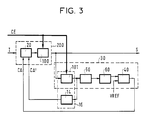
- FIG. 3 illustrates an advantageous mode of defining the gain of the level adjustment circuit, by controlling the gain of the output amplifier 100 by means of said external control CE, and by controlling the attenuation provided by the attenuator 20 by means of said control loop 30.
- the attenuator 20 is provided with a second control input, receiving in this case the control command CA ′.
- the elements M1 and M2 are in this case field effect transistors, the grid of which receives the signal from the comparator 40 and the signal from the amplitude adaptation means 14, respectively.
- the conduction of the transistor M2 is such that the weakening of the attenuator 20 is modified so as to reduce this instantaneous amplitude.
- the high-pass filter in this case constituted by a capacitor CI, inserted between the output of the amplifier 100 and the input of the amplifier 101 has the role of eliminating the voltage of " offset "of amplifier 100.
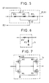
- FIG. 5 represents a diagram of possible embodiment of such controllable feedback resistors R1 and R3 simultaneously so as to permanently keep the gain product of amplifiers 100 and 101 substantially independent of the level selected for the output signal,
- This diagram consists of an association of a certain number of fixed resistors, in this case three resistors, R10, R11, R12, according to a configuration modifiable by action on a certain number of controllable switches, in this case two switches I1 , I2 controlled respectively by binary signals CE1, CE2 so that when these two switches are open, these three resistors are associated in series, hence for the whole a resistance value Rmax, only when one of these two switches is open and the other closed, two of these three resistors in series are short-circuited, the whole being equivalent to a single resistance, hence for the whole an average resistance value Rmoy, and that when these two switches are closed, these three resistors are associated in parallel, hence for the whole a minimum resistance value Rmin.
- the amplitude adaptation means 14 shown in the figure 6 comprise a voltage divider formed by means of two resistors R15, R13.
- the amplitude adaptation means 14 shown in FIG. 7 comprise a threshold device formed by association of two assemblies each formed by association in series of two field effect transistors of opposite types, respectively M3, M4 and M5, M6 and known to each perform a function of inverting a signal applied to its input.
- the input of the first assembly M3, M4 constitutes the input of these amplitude adaptation means
- the output of the first assembly is applied to the input of the second assembly M5, M6
- the output of the second assembly constitutes the output of these amplitude adaptation means.
- the supply voltages of transistors of the same type are also identical, one of these supply voltages being marked VDD and the other being in this case the reference voltage shown here by the ground, and transistors of opposite types have symmetrical characteristics.
- one or other of the transistors M3 and M4 conducts, which results in the conduction of one or more the other respectively of the transistors M6 and M5 in which case the signal obtained at the output of these amplitude adaptation means is a function of the input signal and the conduction characteristics of the transistors used.
Abstract
Description
La présente invention concerne un dispositif de réglage automatique de niveau d'un signal, dit incident, reçu par ce dispositif, fournissant en réponse un signal dit de sortie de niveau sensiblement égal, quelles que soient les variations du signal incident, à un niveau constant éventuellement sélectionnable parmi "n" niveaux possibles.The present invention relates to a device for automatically adjusting the level of a so-called incident signal received by this device, providing in response a so-called output signal of substantially equal level, whatever the variations of the incident signal, at a constant level. possibly selectable among "n" possible levels.
Il est connu de réaliser un tel dispositif de réglage automatique suivant le schéma de la figure 1, où la référence 1 désigne un amplificateur, dit de sortie, dont le niveau du signal de sortie, S, est à régler de façon automatique, et où la référence 2 désigne un atténuateur qui reçoit le signal incident, I, fournit en réponse le signal d'entrée de l'amplificateur de sortie 1, et est en outre commandé par une commande dite d'asservissement CA élaborée par une boucle d'asservissement 3, de façon à maintenir le niveau du signal d'entrée de l'amplificateur 1 constant quel que soit le niveau du signal incident I. Cette boucle d'asservissement comporte elle-même un comparateur, amplificateur 4 qui compare, par rapport à un niveau de référence VREF, le niveau du signal de sortie de cet atténuateur, après redressement dans un redresseur 5 et filtrage dans un filtre passe-bas 6.It is known to produce such an automatic adjustment device according to the diagram in FIG. 1, where the
Suivant la valeur des niveaux à obtenir pour les applications considérées, il peut être nécessaire d'amplifier les signaux avant redressement et filtrage dans la boucle d'asservissement. Sur la figure 1, une telle amplification est réalisée par un amplificateur 10, dit amplificateur de boucle, à gain constant.Depending on the value of the levels to be obtained for the applications considered, it may be necessary to amplify the signals before rectification and filtering in the control loop. In FIG. 1, such an amplification is carried out by an
Sur la figure 1, le niveau de sortie de l'amplificateur 1 est en outre sélectionnable parmi "n" niveaux possibles, ce qui est en l'occurrence obtenu par une commando correspondante CE du gain de l'amplificateur 1, dite commando externe.In FIG. 1, the output level of the
Le schéma ainsi rappelé présente certains inconvénients. En effet, suivant la constante de temps du filtre passe-bas 6, la boucle d'asservissement 3 est plus ou moins efficace contre d'éventuelles surtensions apparaissant sur le signal incident.The scheme thus recalled has certain drawbacks. Indeed, depending on the time constant of the low-
En outre, lorsque le redresseur est un redresseur simple alternance, ce qui a pour avantage de procurer une simplification au plan de la réalisation de ce redresseur, cette boucle d'asservissement n'est pas non plus efficace contre d'éventuelles surtensions apparaissant dans les alternances du signal incident non prises en compte par ce redresseur, notamment à la mise en service du dispositif ou aux changements de fréquences se produisant dans ledit signal incident.In addition, when the rectifier is a simple rectifier alternation, which has the advantage of providing a simplification in terms of the production of this rectifier, this control loop is also not effective against possible overvoltages appearing in the alternations of the incident signal not taken into account by this rectifier, in particular when the device is put into service or at frequency changes occurring in said incident signal.
La présente invention a pour objet un dispositif de réglage automatique de niveau d'un signal dit incident reçu par ce dispositif, fournissant en réponse un signal dit de sortie de niveau sensiblement égal, quelles que soient les variations du signal incident, à un niveau constant éventuellement sélectionnable parmi "n" niveaux possibles (n, nombre entier supérieur à 1) en fonction d'une commande externe de gain appliquée audit dispositif, comportant un circuit de réglage de niveau muni d'une boucle d'asservissement de gain qui élabore une commande fonction du niveau du signal de sortie et éventuellement commandé en outre par ladite commande externe de gain pour fournir, en réponse audit signal incident, ledit signal de sortie, essentiellement caractérisé en ce que ladite boucle d'asservissement de gain qui élabore une commande fonction du niveau du signal de sortie étant dite première boucle, ledit circuit de réglage de niveau est en outre muni d'une seconde boucle d'asservissement de gain qui élabore une commande fonction de l'amplitude instantanée du signal de sortie.The subject of the present invention is an automatic level adjustment device for a so-called incident signal received by this device, providing in response a so-called output signal of substantially equal level, whatever the variations of the incident signal, at a constant level. optionally selectable from "n" possible levels (n, integer greater than 1) according to an external gain control applied to said device, comprising a level adjustment circuit provided with a gain control loop which generates a control depending on the level of the output signal and optionally further controlled by said external gain control to provide, in response to said incident signal, said output signal, essentially characterized in that said gain control loop which generates a function control the level of the output signal being said first loop, said level adjustment circuit is further provided with a second loop the gain control which develops a command as a function of the instantaneous amplitude of the output signal.
D'autres objets et caractéristiques de la présente invention apparaîtront à la lecture de la description suivante d'un exemple de réalisation, faite en relation avec les dessins ci-annexés dans lesquels, outre la figure 1 déjà décrite, et relative à l'art antérieur :
- la figure 2 est un schéma synoptique d'un dispositif de réglage automatique de niveau d'un signal incident, suivant l'invention,
- la figure 3 est un schéma synoptique d'un dispositif de réglage automatique suivant l'invention, illustrant un mode possible de commande de gain du circuit dit de réglage et d'un amplificateur dit de boucle inclus dans ladite première boucle,
- la figure 4 est un schéma de réalisation possible d'un dispositif de réglage automatique de niveau d'un signal incident correspondant au schéma synoptique de la figure 3,
- la figure 5 est un schéma de réalisation possible du mode de commande simultanée du gain du circuit dit de réglage de niveau et de l'amplificateur dit de boucle, par ladite commande externe de gain, tel qu'illustré sur la figure 3,
- la figure 6 est un premier schéma de réalisation possible de moyens d'adaptation d'amplitude pouvant être inclus dans ladite seconde boucle d'asservissement,
- la figure 7 est un deuxième schéma de réalisation possible de tels moyens d'adaptation d'amplitude.
- FIG. 2 is a block diagram of an automatic level adjustment device for an incident signal, according to the invention,
- FIG. 3 is a block diagram of an automatic adjustment device according to the invention, illustrating a possible mode of gain control of the so-called adjustment circuit and of a so-called loop amplifier included in said first loop,
- FIG. 4 is a possible diagram of an automatic level adjustment device for an incident signal corresponding to the block diagram of FIG. 3,
- FIG. 5 is a possible diagram of the mode of simultaneous control of the gain of the so-called level adjustment circuit and of the so-called loop amplifier, by said external gain control, as illustrated in FIG. 3,
- FIG. 6 is a first possible diagram of embodiment of amplitude adaptation means which can be included in said second control loop,
- Figure 7 is a second possible embodiment of such amplitude adaptation means.
Le schéma synoptique d'un dispositif de réglage automatique suivant l'invention illustré sur la figure 2 comporte à titre d'exemple un atténuateur, repéré ici 20 et recevant le signal incident I, et un amplificateur dit de sortie, repéré 100, et fournissant, en réponse au signal issu de cet atténuateur, ledit signal de sortie. Ces deux éléments forment un ensemble 200 appelé circuit de réglage de niveau, qui suivant l'application envisagée, pourrait éventuellement se réduire à un seul de ces éléments.The block diagram of an automatic adjustment device according to the invention illustrated in FIG. 2 includes by way of example an attenuator, marked here 20 and receiving the incident signal I, and a so-called output amplifier, marked 100, and providing , in response to the signal from this attenuator, said output signal. These two elements form an
Ce circuit de réglage de niveau est commandé d'une part par une commande d'asservissement de gain, CA, en vue de fournir un signal de sortie S de niveau sensiblement constant, quelles que soient les variations de niveau du signal incident, et d'autre part par une commande externe de gain, CE, en vue de sélectionner ce niveau parmi "n" niveaux possibles.This level adjustment circuit is controlled on the one hand by a gain control command, CA, in order to provide an output signal S of substantially constant level, whatever the variations in level of the incident signal, and d on the other hand by an external gain control, CE, in order to select this level among "n" possible levels.
La boucle d'asservissement, repérée ici 30, fournissant ladite commande d'asservissement, comporte dans l'ordre, un redresseur 50, un filtre passe-bas 60, et un comparateur-amplificateur 40 qui compare le niveau de signal obtenu en sortie du filtre passe-bas 60 à un niveau de référence fixe VREF.The servo loop, identified here 30, providing said servo control, comprises, in order, a
La boucle d'asservissement 30 est en l'occurence alimentée par le signal de sortie S qui est appliqué dans cette boucle à un amplificateur 101, dit de boucle, dont le gain est commandé, avec celui du circuit de réglage de niveau 200, par ladite commande externe CE, de telle sorte que le produit des gains du circuit de réglage de niveau et de l'amplificateur de boucle soit sensiblement indépendant du niveau sélectionné pour le signal de sortie.The
Suivant l'invention, le schéma synoptique de la figure 2 inclut une seconde boucle d'asservissement de gain, 16, du circuit de réglage de niveau en fonction de l'amplitude instantanée du signal de sortie, permettant d'éviter les inconvénients dus au temps de réaction de la boucle d'asservissement 30 et/ou à la non prise en compte de l'une des alternances du signal incident dans cette première boucle d'asservissement lorsque le redresseur utilisé dans cette boucle est un redresseur simple-alternance. Cette seconde boucle d'asservissement 16 élabore une commande d'asservissement de gain, CA', du circuit de réglage de niveau 200, en l'occurence à partir du signal issu de l'amplificateur 101 mais non redressé, de façon à tenir compte, pour ce second asservissement, d'éventuelles surtensions présentes dans le signal incident, notamment celles des alternances non prise en compte par le redresseur 50 lorsque celui-ci est un redresseur simple alternance.According to the invention, the block diagram of FIG. 2 includes a second gain control loop, 16, of the level adjustment circuit as a function of the instantaneous amplitude of the output signal, making it possible to avoid the drawbacks due to the reaction time of the
Cette seconde boucle d'asservissement peut comporter, en fonction de l'amplitude nécessaire à la commande de gain du circuit de réglage, des moyens 14 d'adapatation d'amplitude.This second control loop may comprise, as a function of the amplitude necessary for the gain control of the adjustment circuit, means 14 for amplitude adaptation.
La figure 3 illustre un mode avantageux de définition du gain du circuit de réglage de niveau, par commande du gain de l'amplificateur de sortie 100 au moyen de ladite commande externe CE, et par asservissement de l'atténuation procurée par l'atténuateur 20 au moyen de ladite boucle d'asservissement 30. Dans ce mode, l'atténuateur 20 est muni d'une deuxième entrée d'asservissement, recevant en l'occurrence la commande d'asservissement CA′.FIG. 3 illustrates an advantageous mode of defining the gain of the level adjustment circuit, by controlling the gain of the
Il n'en demeure pas moins que d'autres modes de réalisation sont possibles. On peut, par exemple, inverser les commandes repérées CA-CA′ avec la commande repérée CE, ce qui revient à utiliser ladite commande externe CE pour jouer sur l'atténuation procurée par l'atténuateur 20 et commander le gain de l'amplificateur de sortie 100 au moyen desdites commandes d'asservissement CA-CA′. On peut aussi en fonction de l'application envisagée, appliquer les deux types de commande de façon conjointe sur un seul des deux éléments constituant le circuit de réglage de niveau ou éventuellement sur le seul élément pouvant constituer le circuit de réglage de niveau.The fact remains that other embodiments are possible. One can, for example, reverse the commands marked CA-CA ′ with the command marked CE, which amounts to using said external command CE to play on the attenuation provided by the
On décrit maintenant, en relation avec la figure 4, un schéma de réalisation possible d'un dispositif suivant la figure 3.A description is now given, in relation to FIG. 4, of a possible embodiment of a device according to FIG. 3.
On retrouve sur cette figure :
- l'amplificateur de
sortie 100, qui est en l'occurrence un amplificateur opérationnel AI muni d'une résistance de contre-réaction commandable R1, et ayant en l'occurrence son entrée additive, notée "+", mise à la tension de référence, schématisée ici par la masse, son entrée soustractive notée "-", recevant le signal de sortie de l'atténuateur 20 via une résistance d'entrée R2, et sa sortie fournissant le signal de sortie S de ce dispositif, - l'amplificateur de
boucle 101, qui est également en l'occurrence un amplificateur opérationnel, A2, muni d'une résistance de contre-réaction commandable R3, et ayant en l'occurrence son entrée additive, notée "+", également à la tension de référence, schématisé ici par la masse, son entrée soustractive, notée "-", connectée à la sortie de l'amplificateur, desortie 100 à travers un filtre passe-haut (condensateur CI en série avec une résistance d'entrée R4), - le
redresseur 50, en l'occurence un redresseur simple alternance formé par exemple d'une diode reliée à la sortie de l'amplificateur deboucle 101, - le filtre passe-bas 60, connecté en sortie du
redresseur 50 et formé en l'occurrence d'une cellule R-C comportant une résistance série R5 et un condensateur parallèle C2, cette cellule présentant une faible constante de temps vis à vis de celle constituée du même condensateur C2 et de la résistance R7 d'entrée ducomparateur 40, - le
comparateur 40, qui est en l'occurrence un amplificateur opérationnel A3 muni d'une résistance de contre-réaction R6, et ayant dans le cas présent son entrée additive, notée "+", mise à un niveau de référence VREF, et son entrée soustractive, notée "-", connectée à la sortie du filtre passe-bas 6 au travers de ladite résistance R7, - l'atténuateur 20, qui est en l'occurrence un diviseur de tension formé d'une résistance série fixe R8 et d'une impédance parallèle variable constituée ici de trois éléments en parallèle M1, M2 et R9 où R9 désigne une résistance fixe et M1 et M2 deux éléments d'impédance commandable, la tension d'entrée de ce diviseur de tension étant formée du signal incident I, et la tension de sortie de ce diviseur de tension, constituant la tension appliquée en l'occurrence à l'entrée soustractive de l'amplificateur 100, étant prise aux bornes de l'impédance commandable que forment les trois éléments en parallèle M1, M2, R9,
- le moyen d'adaptation d'amplitude 14 de la seconde boucle d'asservissement, dont l'entrée est reliée à la sortie de l'amplificateur de
boucle 101 et dont la sortie est appliquée à l'entrée de commande d'asservissement de l'élément M2 de l'atténuateur 20, la sortie ducomparateur 40 étant quant à elle appliquée à l'entrée de commande d'asservissement de l'élément M1 de l'atténuateur 20.
- the
output amplifier 100, which is in this case an operational amplifier AI provided with a controllable feedback resistance R1, and in this case having its additive input, denoted "+", set to the reference voltage , diagrammed here by the ground, its subtractive input denoted "-", receiving the output signal from theattenuator 20 via an input resistor R2, and its output providing the output signal S of this device, - the
loop amplifier 101, which is also in this case an operational amplifier, A2, provided with a controllable feedback resistance R3, and having in this case its additive input, denoted "+", also in the reference voltage, shown here by the ground, its subtractive input, marked "-", connected to the amplifier output, output 100 through a high-pass filter (capacitor CI in series with an input resistance R4 ), - the
rectifier 50, in this case a single alternating rectifier formed for example of a diode connected to the output of theloop amplifier 101, - the low-
pass filter 60, connected at the output of therectifier 50 and in this case formed by an RC cell comprising a series resistor R5 and a parallel capacitor C2, this cell having a low time constant with respect to that consisting of the same capacitor C2 and of the input resistance R7 of thecomparator 40, -
comparator 40, which in this case is an operational amplifier A3 provided with a feedback resistance R6, and in this case having its additive input, denoted "+", brought to a reference level V REF , and its subtractive input, marked "-", connected to the output of the low-pass filter 6 through said resistor R7, - the
attenuator 20, which in this case is a voltage divider formed by a fixed series resistance R8 and an impedance variable parallel formed here of three elements in parallel M1, M2 and R9 where R9 denotes a fixed resistance and M1 and M2 two elements of controllable impedance, the input voltage of this voltage divider being formed of the incident signal I, and the output voltage of this voltage divider, constituting the voltage applied in this case to the subtractive input of theamplifier 100, being taken across the controllable impedance formed by the three elements in parallel M1, M2, R9, - the amplitude adaptation means 14 of the second servo loop, the input of which is connected to the output of the
loop amplifier 101 and the output of which is applied to the servo control input of the the element M2 of theattenuator 20, the output of thecomparator 40 being applied to the servo control input of the element M1 of theattenuator 20.
Les éléments M1 et M2 sont en l'occurrence des transistors à effet de champ dont la grille reçoit respectivement le signal issu du comparateur 40 et le signal issu du moyen d'adaptation d'amplitude 14.The elements M1 and M2 are in this case field effect transistors, the grid of which receives the signal from the
Ainsi, lorsque l'écart entre le niveau du signal représentatif du signal incident, appliqué sur le comparateur 40, et le niveau de référence VREF, augmente, la conduction du transistor M1 est modifiée, ce qui entraîne une modification de l'affaiblissement de l'atténuateur 20 qui va tendre à réduire cet écart.Thus, when the difference between the level of the signal representative of the incident signal, applied to the
De même lorsque l'amplitude instantanée du signal issu du moyen d'adaptation de niveau 14 dépasse un certain seuil, la conduction du transistor M2 est telle que l'affaiblissement de l'atténuateur 20 se trouve modifié de façon à réduire cette amplitude instantanée.Similarly, when the instantaneous amplitude of the signal from the level adaptation means 14 exceeds a certain threshold, the conduction of the transistor M2 is such that the weakening of the
En outre, il apparaît dans le montage ainsi décrit en relation avec la figure 4 que les signaux de sortie de l'amplificateur-comparateur 40 sont inversés par rapport aux signaux de sortie de l'amplificateur de boucle 101; ceci permet à la seconde boucle d'asservissement d'être efficace sur celles des alternances du signal incident qui ne sont pas prises en compte par le redresseur simple-alternance 50; ceci malgré l'utilisation de deux transistors à effet de champ, M1-M2, de même type.Furthermore, it appears in the assembly thus described in relation to FIG. 4 that the output signals of the
On notera par ailleurs que le filtre passe-haut, constitué en l'occurrence par un condensateur CI, inséré entre la sortie de l'amplificateur 100 et l'entrée de l'amplificateur 101 a pour rôle d'éliminer la tension d'"offset" de l'amplificateur 100.It will also be noted that the high-pass filter, in this case constituted by a capacitor CI, inserted between the output of the
Le gain des amplificateurs 100 et 101 s'exprimant sur le schéma de la figure 4 en fonction respectivement des résistances de contre-réaction R1 et R3, la figure 5 représente un schéma de réalisation possible de telles résistances de contre-réaction R1 et R3 commandables simultanément de façon à garder en permanence le produit des gains des amplificateurs 100 et 101 sensiblement indépendant du niveau sélectionné pour le signal de sortie,The gain of the
Ce schéma consiste en une association d'un certain nombre de résistances fixes, en l'occurrence trois résistances, R10, R11, R12, suivant une configuration modifiable par action sur un certain nombre d'interrupteurs commandables, en l'occurrence deux interrupteurs I1, I2 commandés respectivement par des signaux binaires CE1, CE2 de façon que lorsque ces deux interrupteurs sont ouverts, ces trois résistances se trouvent associées en série, d'où pour l'ensemble une valeur de résistance Rmax, que lorsque l'un de ces deux interrupteurs est ouvert et l'autre fermé, deux de ces trois résistances en série soient court-circuitées, l'ensemble étant équivalent à une seule résistance, d'où pour l'ensemble une valeur de résistance moyenne Rmoy, et que lorsque ces deux interrupteurs sont fermés, ces trois résistances se trouvent associées en parallèle, d'où pour l'ensemble une valeur de résistance minimale Rmin.This diagram consists of an association of a certain number of fixed resistors, in this case three resistors, R10, R11, R12, according to a configuration modifiable by action on a certain number of controllable switches, in this case two switches I1 , I2 controlled respectively by binary signals CE1, CE2 so that when these two switches are open, these three resistors are associated in series, hence for the whole a resistance value Rmax, only when one of these two switches is open and the other closed, two of these three resistors in series are short-circuited, the whole being equivalent to a single resistance, hence for the whole an average resistance value Rmoy, and that when these two switches are closed, these three resistors are associated in parallel, hence for the whole a minimum resistance value Rmin.
Les signaux de commande CE1 et CE2 des interrupteurs I1 et I2 étant inversés pour les deux amplificateurs 100 et 101, et la valeur absolue du gain G₁ de l'amplificateur 100 s'exprimant en l'occurrence sous la forme![]()
![]()
![]()
![]()
Les moyens d'adaptation d'amplitude 14 représentés sur la figure 6 comportent un diviseur de tension formé au moyen de deux résistances R15, R13.The amplitude adaptation means 14 shown in the figure 6 comprise a voltage divider formed by means of two resistors R15, R13.
Les moyens d'adaptation d'amplitude 14 représentés sur la figure 7 comportent un dispositif à seuil formé par association de deux montages formés chacun par association en série de deux transistors à effet de champ de types opposés, respectivement M3, M4 et M5, M6 et connus pour réaliser chacun une fonction d'inversion d'un signal appliqué à son entrée. L'entrée du premier montage M3, M4 constitue l'entrée de ces moyens d'adaptation d'amplitude, la sortie du premier montage est appliquée à l'entrée du deuxième montage M5, M6 et la sortie du deuxième montage constitue la sortie de ces moyens d'adaptation d'amplitude. Les tensions d'alimentation de transistors de même type sont en outre identiques, l'une de ces tensions d'alimentation étant repérée VDD et l'autre étant en l'occurrence la tension de référence schématisée ici par la masse, et des transistors de type opposés présentent des caractéristiques symétriques.The amplitude adaptation means 14 shown in FIG. 7 comprise a threshold device formed by association of two assemblies each formed by association in series of two field effect transistors of opposite types, respectively M3, M4 and M5, M6 and known to each perform a function of inverting a signal applied to its input. The input of the first assembly M3, M4 constitutes the input of these amplitude adaptation means, the output of the first assembly is applied to the input of the second assembly M5, M6 and the output of the second assembly constitutes the output of these amplitude adaptation means. The supply voltages of transistors of the same type are also identical, one of these supply voltages being marked VDD and the other being in this case the reference voltage shown here by the ground, and transistors of opposite types have symmetrical characteristics.
Suivant le signe et la valeur absolue de l'amplitude du signal d'entrée de ces moyens d'adaptation d'amplitude, l'un ou l'autre des transistors M3 et M4 conduit, ce qui entraîne la conduction de l'un ou l'autre respectivement des transistors M6 et M5 auquel cas le signal obtenu en sortie de ces moyens d'adaptation d'amplitude est fonction du signal d'entrée et des caractéristiques de conduction des transistors utilisés.Depending on the sign and the absolute value of the amplitude of the input signal of these amplitude adaptation means, one or other of the transistors M3 and M4 conducts, which results in the conduction of one or more the other respectively of the transistors M6 and M5 in which case the signal obtained at the output of these amplitude adaptation means is a function of the input signal and the conduction characteristics of the transistors used.
Claims (12)
Applications Claiming Priority (2)
| Application Number | Priority Date | Filing Date | Title |
|---|---|---|---|
| FR9103645 | 1991-03-26 | ||
| FR9103645A FR2674707B1 (en) | 1991-03-26 | 1991-03-26 | DEVICE FOR AUTOMATICALLY ADJUSTING THE LEVEL OF A SIGNAL. |
Publications (2)
| Publication Number | Publication Date |
|---|---|
| EP0506547A1 true EP0506547A1 (en) | 1992-09-30 |
| EP0506547B1 EP0506547B1 (en) | 1995-05-10 |
Family
ID=9411133
Family Applications (1)
| Application Number | Title | Priority Date | Filing Date |
|---|---|---|---|
| EP92400796A Expired - Lifetime EP0506547B1 (en) | 1991-03-26 | 1992-03-24 | Device for the automatic control of a signal level |
Country Status (5)
| Country | Link |
|---|---|
| EP (1) | EP0506547B1 (en) |
| AT (1) | ATE122509T1 (en) |
| DE (1) | DE69202382T2 (en) |
| ES (1) | ES2072722T3 (en) |
| FR (1) | FR2674707B1 (en) |
Cited By (1)
| Publication number | Priority date | Publication date | Assignee | Title |
|---|---|---|---|---|
| WO2000079748A1 (en) * | 1999-06-23 | 2000-12-28 | At & T Wireless Services, Inc. | Automatic gain control for ofdm receiver |
Citations (3)
| Publication number | Priority date | Publication date | Assignee | Title |
|---|---|---|---|---|
| GB2097619A (en) * | 1980-07-31 | 1982-11-03 | Min Mart V | Stage converter of electric signals |
| US4531229A (en) * | 1982-10-22 | 1985-07-23 | Coulter Associates, Inc. | Method and apparatus for improving binaural hearing |
| US4771472A (en) * | 1987-04-14 | 1988-09-13 | Hughes Aircraft Company | Method and apparatus for improving voice intelligibility in high noise environments |
Family Cites Families (1)
| Publication number | Priority date | Publication date | Assignee | Title |
|---|---|---|---|---|
| JPS5937716A (en) * | 1982-08-26 | 1984-03-01 | Seiko Instr & Electronics Ltd | Automatic gain control circuit |
-
1991
- 1991-03-26 FR FR9103645A patent/FR2674707B1/en not_active Expired - Fee Related
-
1992
- 1992-03-24 EP EP92400796A patent/EP0506547B1/en not_active Expired - Lifetime
- 1992-03-24 ES ES92400796T patent/ES2072722T3/en not_active Expired - Lifetime
- 1992-03-24 DE DE69202382T patent/DE69202382T2/en not_active Expired - Fee Related
- 1992-03-24 AT AT92400796T patent/ATE122509T1/en not_active IP Right Cessation
Patent Citations (3)
| Publication number | Priority date | Publication date | Assignee | Title |
|---|---|---|---|---|
| GB2097619A (en) * | 1980-07-31 | 1982-11-03 | Min Mart V | Stage converter of electric signals |
| US4531229A (en) * | 1982-10-22 | 1985-07-23 | Coulter Associates, Inc. | Method and apparatus for improving binaural hearing |
| US4771472A (en) * | 1987-04-14 | 1988-09-13 | Hughes Aircraft Company | Method and apparatus for improving voice intelligibility in high noise environments |
Non-Patent Citations (1)
| Title |
|---|
| PATENT ABSTRACTS OF JAPAN vol. 8, no. 127 (E-250)(1564) 14 Juin 1984 & JP-A-59 037 716 ( SEIKO DENSHI KOGYO ) * |
Cited By (4)
| Publication number | Priority date | Publication date | Assignee | Title |
|---|---|---|---|---|
| WO2000079748A1 (en) * | 1999-06-23 | 2000-12-28 | At & T Wireless Services, Inc. | Automatic gain control for ofdm receiver |
| US6363127B1 (en) | 1999-06-23 | 2002-03-26 | At&T Wireless Services, Inc. | Automatic gain control methods and apparatus suitable for use in OFDM receivers |
| US6574292B2 (en) | 1999-06-23 | 2003-06-03 | At&T Wireless Services, Inc. | Automatic gain control methods and apparatus suitable for use in OFDM receivers |
| US7065165B2 (en) | 1999-06-23 | 2006-06-20 | Cingular Wireless Ii, Llc | Automatic gain control methods and apparatus suitable for use in OFDM receivers |
Also Published As
| Publication number | Publication date |
|---|---|
| FR2674707B1 (en) | 1993-06-04 |
| ATE122509T1 (en) | 1995-05-15 |
| ES2072722T3 (en) | 1995-07-16 |
| DE69202382T2 (en) | 1995-09-14 |
| FR2674707A1 (en) | 1992-10-02 |
| EP0506547B1 (en) | 1995-05-10 |
| DE69202382D1 (en) | 1995-06-14 |
Similar Documents
| Publication | Publication Date | Title |
|---|---|---|
| EP0326489B1 (en) | Working point regulation system of a dc power supply | |
| FR2471709A1 (en) | TELEPHONE LINE POWER SUPPLY | |
| FR2524756A1 (en) | ||
| FR2511566A1 (en) | THRESHOLD OPTICAL RECEIVER FOR DIGITAL RATE DIGITAL TRANSMISSION SYSTEM | |
| FR2682834A1 (en) | CIRCUIT AND METHOD FOR GENERATING ACCURATE REFERENCE VOLTAGE WITH LOW MEDIUM POWER DISSIPATION. | |
| FR2652697A1 (en) | DIGITAL DATA EXTRACTOR IN A VIDEO SIGNAL. | |
| EP0100514B1 (en) | Device for detecting looping during ringing | |
| EP0278193B1 (en) | Circuit for measuring the dc component of the primary winding current of the output transformer of an inverted rectifier | |
| FR2554989A1 (en) | SERIES VOLTAGE REGULATOR | |
| FR2473234A1 (en) | ELECTRICALLY VARIABLE IMPEDANCE CIRCUIT WITH REACTION COMPENSATION | |
| EP0506547B1 (en) | Device for the automatic control of a signal level | |
| FR2606953A1 (en) | VARIABLE GAIN AMPLIFICATION CIRCUIT AND ITS APPLICATION TO AN AUTOMATIC GAIN CONTROL DEVICE | |
| EP1010048B1 (en) | Voltage regulating circuit for eliminating "latch-up | |
| FR2460576A1 (en) | THREE-TERMINAL POWER SUPPLY CIRCUIT FOR TELEPHONE DEVICE | |
| FR2674706A1 (en) | Device for automatically setting the level of a signal | |
| FR2728074A1 (en) | Detection of electric power consumed by nonlinear load, such as computer peripheral device | |
| EP0042641B1 (en) | Frequency demodulator using a delay circuit, the delay of which varies according to the received frequency | |
| EP0004498A2 (en) | Apparatus for generating the cut-off voltage of a cathode-ray-tube and colour television receiver embodying such an apparatus | |
| FR2645373A1 (en) | METHOD AND DEVICE FOR REDUCING NOISE ON A CODABLE SIGNAL AT SEVERAL PREDETERMINED LEVELS | |
| FR2473826A1 (en) | SYSTEM AND METHOD FOR DATA TRANSMISSION WITH CONTINUOUS CURRENT COUPLING | |
| EP0506186A1 (en) | Video amplifier device | |
| CA1147027A (en) | Very low frequency passband filter circuit | |
| FR2685583A1 (en) | Multi-band frequency synthesizer | |
| FR2626420A1 (en) | DEVICE FOR FREQUENCY SERVICING AN OSCILLATOR | |
| EP0868030B1 (en) | Phase-locked loop with phase lock assistance circuit |
Legal Events
| Date | Code | Title | Description |
|---|---|---|---|
| PUAI | Public reference made under article 153(3) epc to a published international application that has entered the european phase |
Free format text: ORIGINAL CODE: 0009012 |
|
| AK | Designated contracting states |
Kind code of ref document: A1 Designated state(s): AT BE CH DE ES FR GB IT LI NL SE |
|
| 17P | Request for examination filed |
Effective date: 19930322 |
|
| 17Q | First examination report despatched |
Effective date: 19940613 |
|
| GRAA | (expected) grant |
Free format text: ORIGINAL CODE: 0009210 |
|
| AK | Designated contracting states |
Kind code of ref document: B1 Designated state(s): AT BE CH DE ES FR GB IT LI NL SE |
|
| REF | Corresponds to: |
Ref document number: 122509 Country of ref document: AT Date of ref document: 19950515 Kind code of ref document: T |
|
| REF | Corresponds to: |
Ref document number: 69202382 Country of ref document: DE Date of ref document: 19950614 |
|
| ITF | It: translation for a ep patent filed |
Owner name: JACOBACCI & PERANI S.P.A. |
|
| REG | Reference to a national code |
Ref country code: ES Ref legal event code: FG2A Ref document number: 2072722 Country of ref document: ES Kind code of ref document: T3 |
|
| GBT | Gb: translation of ep patent filed (gb section 77(6)(a)/1977) |
Effective date: 19950714 |
|
| PLBE | No opposition filed within time limit |
Free format text: ORIGINAL CODE: 0009261 |
|
| STAA | Information on the status of an ep patent application or granted ep patent |
Free format text: STATUS: NO OPPOSITION FILED WITHIN TIME LIMIT |
|
| 26N | No opposition filed | ||
| REG | Reference to a national code |
Ref country code: GB Ref legal event code: IF02 |
|
| PGFP | Annual fee paid to national office [announced via postgrant information from national office to epo] |
Ref country code: NL Payment date: 20040229 Year of fee payment: 13 |
|
| PGFP | Annual fee paid to national office [announced via postgrant information from national office to epo] |
Ref country code: AT Payment date: 20040303 Year of fee payment: 13 |
|
| PGFP | Annual fee paid to national office [announced via postgrant information from national office to epo] |
Ref country code: SE Payment date: 20040319 Year of fee payment: 13 |
|
| PGFP | Annual fee paid to national office [announced via postgrant information from national office to epo] |
Ref country code: CH Payment date: 20040322 Year of fee payment: 13 |
|
| PGFP | Annual fee paid to national office [announced via postgrant information from national office to epo] |
Ref country code: BE Payment date: 20040511 Year of fee payment: 13 |
|
| PG25 | Lapsed in a contracting state [announced via postgrant information from national office to epo] |
Ref country code: AT Free format text: LAPSE BECAUSE OF NON-PAYMENT OF DUE FEES Effective date: 20050324 |
|
| PG25 | Lapsed in a contracting state [announced via postgrant information from national office to epo] |
Ref country code: SE Free format text: LAPSE BECAUSE OF NON-PAYMENT OF DUE FEES Effective date: 20050325 |
|
| PG25 | Lapsed in a contracting state [announced via postgrant information from national office to epo] |
Ref country code: LI Free format text: LAPSE BECAUSE OF NON-PAYMENT OF DUE FEES Effective date: 20050331 Ref country code: CH Free format text: LAPSE BECAUSE OF NON-PAYMENT OF DUE FEES Effective date: 20050331 Ref country code: BE Free format text: LAPSE BECAUSE OF NON-PAYMENT OF DUE FEES Effective date: 20050331 |
|
| BERE | Be: lapsed |
Owner name: *ALCATEL CIT Effective date: 20050331 |
|
| PG25 | Lapsed in a contracting state [announced via postgrant information from national office to epo] |
Ref country code: NL Free format text: LAPSE BECAUSE OF NON-PAYMENT OF DUE FEES Effective date: 20051001 |
|
| EUG | Se: european patent has lapsed | ||
| REG | Reference to a national code |
Ref country code: CH Ref legal event code: PL |
|
| NLV4 | Nl: lapsed or anulled due to non-payment of the annual fee |
Effective date: 20051001 |
|
| PGFP | Annual fee paid to national office [announced via postgrant information from national office to epo] |
Ref country code: ES Payment date: 20060327 Year of fee payment: 15 |
|
| PGFP | Annual fee paid to national office [announced via postgrant information from national office to epo] |
Ref country code: GB Payment date: 20060329 Year of fee payment: 15 |
|
| PGFP | Annual fee paid to national office [announced via postgrant information from national office to epo] |
Ref country code: DE Payment date: 20070430 Year of fee payment: 16 |
|
| GBPC | Gb: european patent ceased through non-payment of renewal fee |
Effective date: 20070324 |
|
| BERE | Be: lapsed |
Owner name: *ALCATEL CIT Effective date: 20050331 |
|
| PGFP | Annual fee paid to national office [announced via postgrant information from national office to epo] |
Ref country code: IT Payment date: 20070608 Year of fee payment: 16 |
|
| PG25 | Lapsed in a contracting state [announced via postgrant information from national office to epo] |
Ref country code: GB Free format text: LAPSE BECAUSE OF NON-PAYMENT OF DUE FEES Effective date: 20070324 |
|
| PGFP | Annual fee paid to national office [announced via postgrant information from national office to epo] |
Ref country code: FR Payment date: 20070319 Year of fee payment: 16 |
|
| REG | Reference to a national code |
Ref country code: ES Ref legal event code: FD2A Effective date: 20070326 |
|
| PG25 | Lapsed in a contracting state [announced via postgrant information from national office to epo] |
Ref country code: ES Free format text: LAPSE BECAUSE OF NON-PAYMENT OF DUE FEES Effective date: 20070326 |
|
| REG | Reference to a national code |
Ref country code: FR Ref legal event code: ST Effective date: 20081125 |
|
| PG25 | Lapsed in a contracting state [announced via postgrant information from national office to epo] |
Ref country code: DE Free format text: LAPSE BECAUSE OF NON-PAYMENT OF DUE FEES Effective date: 20081001 |
|
| PG25 | Lapsed in a contracting state [announced via postgrant information from national office to epo] |
Ref country code: FR Free format text: LAPSE BECAUSE OF NON-PAYMENT OF DUE FEES Effective date: 20080331 |
|
| PG25 | Lapsed in a contracting state [announced via postgrant information from national office to epo] |
Ref country code: IT Free format text: LAPSE BECAUSE OF NON-PAYMENT OF DUE FEES Effective date: 20080324 |