EP0508604B1 - Disk array controller for data storage system - Google Patents
Disk array controller for data storage system Download PDFInfo
- Publication number
- EP0508604B1 EP0508604B1 EP92302098A EP92302098A EP0508604B1 EP 0508604 B1 EP0508604 B1 EP 0508604B1 EP 92302098 A EP92302098 A EP 92302098A EP 92302098 A EP92302098 A EP 92302098A EP 0508604 B1 EP0508604 B1 EP 0508604B1
- Authority
- EP
- European Patent Office
- Prior art keywords
- bus
- data
- array
- host
- disk
- Prior art date
- Legal status (The legal status is an assumption and is not a legal conclusion. Google has not performed a legal analysis and makes no representation as to the accuracy of the status listed.)
- Expired - Lifetime
Links
Images


Classifications
-
- G—PHYSICS
- G06—COMPUTING; CALCULATING OR COUNTING
- G06F—ELECTRIC DIGITAL DATA PROCESSING
- G06F11/00—Error detection; Error correction; Monitoring
- G06F11/07—Responding to the occurrence of a fault, e.g. fault tolerance
- G06F11/08—Error detection or correction by redundancy in data representation, e.g. by using checking codes
- G06F11/10—Adding special bits or symbols to the coded information, e.g. parity check, casting out 9's or 11's
- G06F11/1076—Parity data used in redundant arrays of independent storages, e.g. in RAID systems
-
- G—PHYSICS
- G06—COMPUTING; CALCULATING OR COUNTING
- G06F—ELECTRIC DIGITAL DATA PROCESSING
- G06F11/00—Error detection; Error correction; Monitoring
- G06F11/07—Responding to the occurrence of a fault, e.g. fault tolerance
- G06F11/08—Error detection or correction by redundancy in data representation, e.g. by using checking codes
- G06F11/10—Adding special bits or symbols to the coded information, e.g. parity check, casting out 9's or 11's
- G06F11/1008—Adding special bits or symbols to the coded information, e.g. parity check, casting out 9's or 11's in individual solid state devices
-
- G—PHYSICS
- G06—COMPUTING; CALCULATING OR COUNTING
- G06F—ELECTRIC DIGITAL DATA PROCESSING
- G06F3/00—Input arrangements for transferring data to be processed into a form capable of being handled by the computer; Output arrangements for transferring data from processing unit to output unit, e.g. interface arrangements
- G06F3/06—Digital input from, or digital output to, record carriers, e.g. RAID, emulated record carriers or networked record carriers
- G06F3/0601—Interfaces specially adapted for storage systems
- G06F3/0668—Interfaces specially adapted for storage systems adopting a particular infrastructure
- G06F3/0671—In-line storage system
- G06F3/0673—Single storage device
Definitions
- the first level RAID comprises N disks for storing data and N additional "mirror" disks for storing copies of the information written to the data disks.
- RAID level 1 write functions require that data be written to two disks, the second "mirror" disk receiving the same information provided to the first disk. When data is read, it can be read from either disk.
- RAID level 3 systems comprise one or more groups of N+1 disks. Within each group, N disks are used to store data, and the additional disk is utilized to store parity information. During RAID level 3 write functions, each block of data is divided into N portions for storage among the N data disks. The corresponding parity information is written to a dedicated parity disk. When data is read, all N data disks must be accessed. The parity disk is used to reconstruct information in the event of a disk failure.
- the host operates as the RAID controller and performs the parity generation and checking. Having the host computer parity is expensive in host processing overhead.
- the known system includes a fixed data path structure interconnecting the plurality of disk drives with the host system. Rearrangement of the disk array system to accommodate different quantities of disk drives or different RAID configurations is not easily accomplished.
- US-A-4,914,656 discloses a data storage system including a host bus means adapted to be connected to a host device, disk drive means adapted to be connected to a plurality of disk drive devices, selectively controllable coupling means connected to the host bus means and to a plurality of buses and which includes connecting means adapted to connect the host bus means to a first group of buses.
- EP-A-0,369,707 discloses a data storage system likewise including a host bus means for connection to a host device, disk drive means for connection to a plurality of disk drive devices and selectively controllable coupling means connected to the host bus means and the disk drive means.
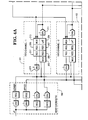
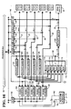
- FIG 2 is a functional block diagram of the SCSI Array Data Path Chip (ADP) shown in Figure 1.
- the ADP chip consists of the following internal functional blocks: control logic block 60 including diagnostic module 62, configuration control and status register module 64, interrupt module 66 and interface module 68; DMA FIFO block 70; and data and parity routing block 100.
- An exclusive-OR circuit 110 is employed to generate parity information from data placed on array busses 21 through 25.
- a tap is provided between each one of array busses 21 through 25 and a first input of a respective two-to-one multiplexer, the output of which forms an input to exclusive-OR circuit 110.
- the second inputs of each one of the multiplexers, identified by reference numerals 111 through 115, are connected to ground.
- transceivers 141 through 146 for connecting respective busses 21 through 26 with processor bus 53 for transferring diagnostic information between the array channels and the processor.
- An additional transceiver 150 connects host busses 16U and 16L with processor bus 53. Transceivers 141 through 146 and 150 allow diagnostic operations by the controller processor.
- Figures 4A through 4F provide additional detail concerning the construction and operation of double registers 101 through 105, transceivers 141 through 146 and transceiver 150, and control of data to and from SCSI bus interface chips 31 through 35 and SRAM 36.
- Control lines are provided between control registers residing in configuration control and status module 64, discussed above, and double registers 101 through 105, multiplexers 111 through 116, tri-state buffers 121 through 126, and transceivers 141 through 146 and 150.
- Five data path control registers are responsible for configuration of the data path.
- Data Path Control Register 1 controls data flow through double registers 101 through 105 during array write operations. Each control register bit controls the operation of one of registers 101 through 105 as identified below.
- Data Path Control Register 1 Bit 0 enables register 101 Bit 1 enables register 102 Bit 2 enables register 103 Bit 3 enables register 104 Bit 4 enables register 105 Bit 5 not used Bit 6 not used Bit 7 not used
- control bits 0 through 4 When any one of control bits 0 through 4 are set high, data obtained from the host is transferred onto the internal array bus corresponding to the enabled register. The data obtained from the host is thereafter available to the SCSI bus interface chip connected to the array bus, the parity generating logic and to the diagnostic circuitry.
- Data path control register 4 through associated chip hardware, enable specific RAID operations as described below.
- Data Path Control Register 4 Bit 0 array data transfer direction Bit 1 RAID level 1 enable Bit 2 RAID level 4 or 5 enable Bit 3 RAID level 3 enable Bit 4 drive configuration 2+1 enable Bit 5 drive configuration 4+1 enable Bit 6 array parity checking enable Bit 7 not used
- the direction of data flow through the register banks 101 through 105 is determined from the setting of bit 0. This bit is set high for host to array write operations and set low for array to host read operations. Bits 1, 2 and 3 enable the specific RAID operations when set high. Bits 4 and 5 enable the specific RAID level 3 operations when set high. Control bit 6 is set high to enable parity checking.
- Double register 102 is enabled to receive the new data from the host and provide the data to the channel 2 disk via bus 22 and enabled SCSI bus interface chip 32.
- the new data is also provided to parity generator 110 through multiplexer 112.
- the information previously written into SRAM 36 is also provided to parity generator 110 through multiplexer 116.
- the output of the parity generator is the new parity which is provided through enabled tri-state buffer 121, bus 21 and enabled SCSI bus interface chip 31 to the channel 1 disk.
- control register 1 - 02hex The contents of the data path control registers for the second portion of the RAID level 5 write operation are as follows: control register 1 - 02hex, control register 2 - 22hex, control register 3 - 23hex, control register 4 - 05hex, and control register 5 - 03hex.
- Figures 17 and 18 show the data path architecture configured for data broadcasting wherein the same data is written to each of the disks in the array. Data broadcasting may be performed to initialize all the array disks with a known data pattern.
- data is received by double register 101 from the processor via bus 53 and enabled transceiver 150.
- data is provided to double register 101 by the host system. In both cases double register 101 is enabled to provide the received data to SCSI bus interface chips 31 via bus 21.
- Multiplexer 111 is enabled to provide bus 21 data to exclusive-OR circuit 110.
- Multiplexers 112 through 116 remain disabled so that the output of circuit 110 is equivalent to the data received from bus 21.
- Tristate devices 112 through 115 are enabled to provide the output of circuit 110 to SCSI bus interface chips 32 through 35.
Abstract
Description
- This invention relates to data storage systems of the kind including host bus means adapted to be connected to a host device, and disk drive means adapted to be connected to a plurality of disk drive devices.
- Recent and continuing increases in computer processing power and speed, in the speed and capacity of primary memory, and in the size and complexity of computer software has resulted in the need for faster operating, larger capacity secondary memory storage devices; magnetic disks forming the most common external or secondary memory storage means utilized in present day computer systems. Unfortunately, the rate of improvement in the performance of large magnetic disks has not kept pace with processor and main memory performance improvements. However, significant secondary memory storage performance and cost improvements may be obtained by the replacement of single large expensive disk drives with a multiplicity of small, inexpensive disk drives interconnected in a parallel array, which to the host appears as a single large fast disk.
- Several disk array design alternatives were presented in an article titled "A Case for Redundant Arrays of Inexpensive Disks (RAID)" by David A. Patterson, Garth Gibson and Randy H. Katz; University of California Report No. UCB/CSD 87/391, December 1987. This article discusses disk arrays and the improvements in performance, reliability, power consumption and scalability that disk arrays provide in comparison to single large magnetic disks.
- Five disk array arrangements, referred to as RAID levels, are described in the article. The first level RAID comprises N disks for storing data and N additional "mirror" disks for storing copies of the information written to the data disks.
RAID level 1 write functions require that data be written to two disks, the second "mirror" disk receiving the same information provided to the first disk. When data is read, it can be read from either disk. -
RAID level 3 systems comprise one or more groups of N+1 disks. Within each group, N disks are used to store data, and the additional disk is utilized to store parity information. DuringRAID level 3 write functions, each block of data is divided into N portions for storage among the N data disks. The corresponding parity information is written to a dedicated parity disk. When data is read, all N data disks must be accessed. The parity disk is used to reconstruct information in the event of a disk failure. -
RAID level 4 systems are also comprised of one or more groups of N+1 disks wherein N disks are used to store data, and the additional disk is utilized to store parity information.RAID level 4 systems differ fromRAID level 3 systems in that data to be saved is divided into larger portions, consisting of one or many blocks of data, for storage among the disks. Writes still require access to two disks, i.e., one of the N data disks and the parity disk. In a similar fashion, read operations typically need only access a single one of the N data disks, unless the data to be read exceeds the block length stored on each disk. As withRAID level 3 systems, the parity disk is used to reconstruct information in the event of a disk failure. -
RAID level 5 is similar toRAID level 4 except that parity information, in addition to the data, is distributed across the N+1 disks in each group. Although each group contains N+1 disks, each disk includes some blocks for storing data and some blocks for storing parity information. Where parity information is stored is controlled by an algorithm implemented by the user. As inRAID level 4 systems,RAID level 5 writes require access to at least two disks; however, no longer does every write to a group require access to the same dedicated parity disk, as inRAID level 4 systems. This feature provides the opportunity to perform concurrent write operations. - In a known disk array system the host operates as the RAID controller and performs the parity generation and checking. Having the host computer parity is expensive in host processing overhead. Furthermore, the known system includes a fixed data path structure interconnecting the plurality of disk drives with the host system. Rearrangement of the disk array system to accommodate different quantities of disk drives or different RAID configurations is not easily accomplished.
- US-A-4,914,656 discloses a data storage system including a host bus means adapted to be connected to a host device, disk drive means adapted to be connected to a plurality of disk drive devices, selectively controllable coupling means connected to the host bus means and to a plurality of buses and which includes connecting means adapted to connect the host bus means to a first group of buses. EP-A-0,369,707 discloses a data storage system likewise including a host bus means for connection to a host device, disk drive means for connection to a plurality of disk drive devices and selectively controllable coupling means connected to the host bus means and the disk drive means.
- EP-A-0,294,287 and EP-A-0,320,107 relate to data storage systems of the type defined within the present application but all of these aforementioned systems are disadvantageously restricted having regard to their adaptability and versatility for controlling data flow between a host and a disk array.
- It is an object of the present invention to provide a data storage system of the kind specified which may be readily adapted to support various disk drive array configurations.
- Therefore, according to the present invention, there is provided a data storage system. including host bus means adapted to be connected to a host device, disk drive means adapted to be connected to a plurality of disk drive devices, selectively controllable coupling means connected to said host bus means and to a plurality of array buses coupled to said disk drive means, first connecting means adapted to connect said host bus means to a first group of selected array buses characterized in that said first connecting means includes a plurality of register means each associated with a respective array bus and connected to said host bus means for receiving data therefrom, each register means having a respective bus driver connected thereto and also connected to the associated array bus, the bus drivers being selectively controllable to connect said host bus means to said first group of selected array buses, and in that said coupling means includes parity generation means, second connecting means adapted to connect a second group of selected array buses to the input of said parity generation means, and third connecting means adapted to connect the output of said parity generation means to a third group of selected array buses.
- One embodiment of the invention will now be described by way of example, with reference to the accompanying drawings, in which:-
- Figure 1 is a block diagram of a disk array controller incorporating the data and parity routing architecture of the present invention;
- Figure 2 is a functional block diagram of the SCSI Array Data Path Chip (ADP) shown in Figure 1 which incorporates the data and parity routing architecture of the present invention;
- Figure 3 is a block diagram of the DMA FIFO and routing blocks shown in Figure 2, representing a preferred embodiment of the present invention;
- Figures 4A through 4F provide a more detailed block diagram of the architecture shown in Figure 3; and
- Figures 5 through 18 illustrate some of the
various configurations of the circuit of Figure 3.
For example, Figure 8 shows the circuit configuration
for performing a
RAID level 3 write operation. -
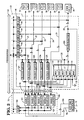
- Referring now to Figure 1, there is seen a block diagram of a SCSI (small computer system interface) disk array controller incorporating the data and parity routing architecture of the present invention. The controller includes a
host SCSI adapter 14 to interface between the hostsystem data bus 12 andSCSI data bus 16. Parity generation and data and parity routing are performed within SCSI Array Data Path Chip (ADP) 10.ADP chip 10 interconnectsSCSI data bus 16 with six additional data busses, identified byreference numerals 21 through 26. SCSIbus interface chips 31 through 35 interface between respective SCSI data busses 21 through 25 and corresponding external disk drive data busses 41 through 45.Bus 26 connectsADP chip 10 with a 64 kilobyte static random access memory (SRAM) 36. ADPchip 10,SCSI adapter 14 and SCSIbus interface chips 31 through 35 all operate under the control of adedicated microprocessor 51. - All data busses shown, with the exception of
bus 16, include nine data lines, one of which is a parity bit line.Bus 16 includes 18 data lines, two of which are bus parity lines. Additional control, acknowledge and message lines, not shown, are also included with the data busses. -
SCSI adapter 14, SCSIbus interface chips 31 through 36, SRAM 36 andmicroprocessor 51 are commercially available items. For example,SCSI adapter 14 may be aFast SCSI 2 chip, SCSIbus interface chips 31 through 35 may be NCR 53C96 chips andmicroprocessor 51 could be a Motorola MC68020, 16 megahertz microprocessor. Also residing on the microprocessor bus are a one megabyte DRAM, a 128 kilobyte EPROM, an eight kilobyte EEPROM, a 68901 multifunction peripheral controller and various registers. - SCSI
data path chip 10 is an application specific integrated circuit device capable of handling all data routing, data multiplexing and demultiplexing, and parity generation and checking aspects ofRAID levels chip 10 handles the transfer of data betweenhost SCSI adapter 14 and SCSIbus interface chips 31 through 35. The ADP chip also handles the movement of data to and from the 64 kilobyte SRAM during read/modify/write operations ofRAID level 5. - Figure 2 is a functional block diagram of the SCSI Array Data Path Chip (ADP) shown in Figure 1. The ADP chip consists of the following internal functional blocks:
control logic block 60 includingdiagnostic module 62, configuration control andstatus register module 64,interrupt module 66 andinterface module 68;DMA FIFO block 70; and data andparity routing block 100. - The main function of
control block 60 is to configure and to test the data path and parity path described in herein.Microprocessor interface module 68 contains basic microprocessor read and write cycle control logic providing communication and data transfer between microprocessor 51 (shown in Figure 1) and control and status registers within the control block. This interface utilizes a multiplexed address and data bus standard wherein microprocessor read and write cycles consist of an address phase followed by a data phase. During the address phase a specific register is selected by the microprocessor. During the following data phase, data is written to or read from the addressed register. - Configuration control and
status register module 64 includes numerous eight-bit registers under the control ofmicroprocessor interface module 68 as outlined above. The contents of the control registers determine the configuration of the data and parity paths. Status registers provide configuration and interrupt information to the microprocessor. -
Diagnostic module 62 includes input and output data registers for the host and each array channel. The input registers are loaded by the processor and provide data to hostbus 16, array busses 21 through 25 andSRAM bus 26 to emulate host or array transfers. The output registers, which are loaded with data routed through the various data buses, are read by the microprocessor to verify the proper operation of selected data and parity path configurations. - Interrupt
module 66 contains the control logic necessary to implement masking and grouping of ADP chip and disk controller channel interrupt signals. Any combination of five channel interrupt signals received from SCSI bus interface chips 31 through 35 and three internally generated ADP parity error interrupt signals can be combined together to generate interrupt signals for the microprocessor. - The function of
DMA FIFO block 70 is to hold data received from the host until the array is ready to accept the data and to convert the data from eighteenbit bus 16 to nine bit busses 18. During read operationsDMA FIFO block 70 holds the data received from the disk array until the host system is ready to accept the data and converts the data from nine bit busses 18 to eighteenbit bus 16. - Data and
parity routing block 100 contains the steering logic for configuring the data and parity paths between the host, the disk array andSRAM 36 in response to control bytes placed into the control registers contained inmodule 64. Block 100 also includes logic for generating and checking parity, verifying data, broadcasting data, monitoring data transfers, and reconstructing data lost due to a single disk drive failure. - Figure 3 is a block diagram of
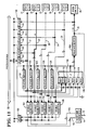
DMA FIFO block 70 androuting block 100 shown in Figure 2, representing a preferred embodiment of the present invention. The data routing architecture includes five data channels, each channel providing a data path betweenSCSI adapter 14 and a corresponding one of SCSI bus interface chips 31 through 35. The first data channel includes adouble register 101 connected between nine-bit host busses 16U and 16L andarray bus 21.Busses external SCSI adapter 14 anddouble register 101.Array bus 21 connectsdouble register 101 with SCSIbus interface chip 31. Additional taps toarray bus 21 will be discussed below. Data channels two through five are similarly constructed, connectinghost busses double registers 102 through 105 and array busses 22 through 25 with SCSI bus interface chips 32 through 35. - Each one of
double registers 101 through 105 includes an internal two-to-one multiplexer for selecting as input either one of host busses 16U or 16L when data is to be transferred frombusses Double registers parity bus 130 when data is to be transferred to hostbusses - An exclusive-
OR circuit 110 is employed to generate parity information from data placed on array busses 21 through 25. A tap is provided between each one of array busses 21 through 25 and a first input of a respective two-to-one multiplexer, the output of which forms an input to exclusive-OR circuit 110. The second inputs of each one of the multiplexers, identified byreference numerals 111 through 115, are connected to ground. - The output of exclusive-
OR circuit 110 is provided via nine-bit bus 130 todouble registers tristate buffers tristate buffers 121 through 126, when enabled, provides the parity information generated by exclusive-OR circuit 110 to a respective one ofbusses 21 through 26.Bus 26 connects the output oftristate buffer 126 withSRAM 36 and one input of a two-to-onemultiplexer 116. The output ofmultiplexer 116 is input to exclusive-OR circuit 110 to provide the architecture with parity checking and data reconstruction capabilities, to be discussed in greater detail below. - Also shown in Figure 3 are six transceivers, identified by
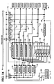
reference numerals 141 through 146, for connectingrespective busses 21 through 26 withprocessor bus 53 for transferring diagnostic information between the array channels and the processor. Anadditional transceiver 150 connects host busses 16U and 16L withprocessor bus 53.Transceivers 141 through 146 and 150 allow diagnostic operations by the controller processor. - Figures 4A through 4F provide additional detail concerning the construction and operation of
double registers 101 through 105,transceivers 141 through 146 andtransceiver 150, and control of data to and from SCSI bus interface chips 31 through 35 andSRAM 36. -
Double register 101 is seen to include amultiplexer 203 for selecting data from either ofbusses registers latch 209 and a buffer/driver 211 for placing the register contents ontoarray bus 21.Double register 101 further includes amultiplexer 213 for selecting data from either ofbusses registers driver 219 for placing the content ofregisters bus 16L.Double register 102 is identical in construction todouble register 101 for transferring data from either ofbusses bus 22, and from either ofbusses bus 16U.Double registers double registers bus 130.Double register 105 includes only those elements described above which are necessary to transfer information frombusses bus 25. - Each one of
transceivers 141 through 146 includes aregister 223 connected to receive and store data residing on the associated array or SRAM bus , a buffer/driver 225 connected to provide the contents ofregister 223 toprocessor bus 53, aregister 227 connected to receive and store data fromprocessor bus 53, and a buffer/driver 229 connected to provide the contents ofregister 227 to the associated array or SRAM bus.Transceiver 150 includes registers and drivers for storing and transferring data betweenprocessor bus 53 and each one ofhost busses - Array busses 21 through 25 each include a pair of parallel-connected buffer/
drivers SRAM bus 26 is similarly connected withSRAM 36. - Control lines, not shown, are provided between control registers residing in configuration control and
status module 64, discussed above, anddouble registers 101 through 105,multiplexers 111 through 116,tri-state buffers 121 through 126, andtransceivers 141 through 146 and 150. Five data path control registers are responsible for configuration of the data path. - Data
Path Control Register 1 controls data flow throughdouble registers 101 through 105 during array write operations. Each control register bit controls the operation of one ofregisters 101 through 105 as identified below.Data Path Control Register 1Bit 0 enables register 101 Bit 1enables register 102 Bit 2enables register 103 Bit 3enables register 104 Bit 4enables register 105 Bit 5not used Bit 6 not used Bit 7 not used - When any one of control bits 0 through 4 are set high, data obtained from the host is transferred onto the internal array bus corresponding to the enabled register. The data obtained from the host is thereafter available to the SCSI bus interface chip connected to the array bus, the parity generating logic and to the diagnostic circuitry.
- Data
Path Control Register 2 controls the operation ofmultiplexers 111 through 116, thereby governing the input to exclusive-OR circuit 110. Each register bit controls the operation of one ofmultiplexers 111 through 116 as identified below.Data Path Control Register 2Bit 0 selects input to MUX 111 Bit 1selects input to MUX 112 Bit 2selects input to MUX 113 Bit 3selects input to MUX 114 Bit 4selects input to MUX 115 Bit 5selects input to MUX 116 Bit 6 not used Bit 7 not used - In the table above, a logic one stored in one or more of register bits 0 through 5 sets the corresponding multiplexer to provide data from its associated array bus to exclusive-
OR circuit 110. A logic zero stored in one or more of register bits 0 through 5 selects the corresponding multiplexer input connected to ground. - Data path control
register 3 enables and disables the flow of data to or from SCSI bus interface chips 31 through 35 andSRAM 36. The functions of the individual register bits are described below.Data Path Control Register 3Bit 0 enable SCSI DMA I/O on channel 1Bit 1enable SCSI DMA I/O on channel 2Bit 2enable SCSI DMA I/O on channel 3Bit 3enable SCSI DMA I/O on channel 4Bit 4enable SCSI DMA I/O on channel 5Bit 5enable data I/O with SRAM Bit 6 not used Bit 7 not used - A logic one stored in any one of bits 0 through 5 enables the corresponding channel. Data flow direction to or from SCSI bus interface chips 31 through 35 and
SRAM 36 is determined by data path controlregister 5. - Data path control
register 4, through associated chip hardware, enable specific RAID operations as described below.Data Path Control Register 4Bit 0 array data transfer direction Bit 1 RAID level 1 enableBit 2RAID level Bit 3RAID level 3 enableBit 4drive configuration 2+1 enableBit 5drive configuration 4+1 enableBit 6 array parity checking enable Bit 7 not used - The direction of data flow through the
register banks 101 through 105 is determined from the setting of bit 0. This bit is set high for host to array write operations and set low for array to host read operations.Bits Bits specific RAID level 3 operations when set high. Control bit 6 is set high to enable parity checking. - Data path control
register 5 controls the data flow direction to or from SCSI bus interface chips 31 through 35 andSRAM 36.Data Path Control Register 5Bit 0 array direction channel 1Bit 1array direction channel 2Bit 2array direction channel 3Bit 3array direction channel 4Bit 4array direction channel 5Bit 5external SRAM direction Bit 6 not used Bit 7 not used - A logic one stored in any one of register bits 0 through 5 specifies that data is to transferred from the array channel bus to its connected SCSI bus interface chip or SRAM. A logic 0 sets the data transfer direction from the SCSI bus interface chip or SRAM to the corresponding array channel bus. The control bits of
register 3 must be set to enable SCSI bus interface chips 31 through 35 ofSRAM 36 to perform a data transfer operation. - The five data path control registers discussed above enable or disable
double registers 101 through 105,multiplexers 111 through 116,tri-state buffers 121 through 126, andtransceivers 141 through 146 and 150 to configure the architecture to perform thevarious RAID levels - Figure 5 shows the data path architecture configured to perform
RAID level 1 write operations onchannels Double registers busses busses bus 16L tobusses bus 16U tobusses busses busses - The
RAID level 1 read configuration is shown in Figure 6. As bothchannel 1 andchannel 2 array disks store the same information only one of the disks need be accessed for aRAID level 1 read. To read data from thechannel 1 disk data path control register contents are set as follows: control register 1 - 00hex, control register 2 - 01hex, control register 3 - 01hex, control register 4 - 02hex, and control register 5 - 00hex. SCSIbus interface chip 31 is enabled to provide data from thechannel 1 disk tobus 21.Multiplexer 111 is enabled to provide the data onbus 21 throughparity generation circuit 110 tobus 130. Sincemultiplexers 112 through 116 are disabled the data provided to multiplexer 111 passes through the parity generator unaltered.Double registers bus 130 tobusses Bus 16U is provided with upper byte information whilebus 16L transmits lower byte information. - Figure 7 shows the data path architecture configured to reconstruct the
RAID level 1channel 1 disk from thechannel 2 disk. Data path control register contents are set as follows: control register 1 - 00hex, control register 2 - 02hex, control register 3 - 03hex, control register 4 - 03hex, and control register 5 - 01hex. SCSIbus interface chip 32 is enabled to provide data tobus 22,multiplexer 112 is enabled to providebus 22 data tobus 130,tristate buffer 121 is enabled to placebus 130 data ontobus 21, and SCSIbus interface chip 31 is enabled to write data received frombus 21 onto thechannel 1 disk. The architecture could similarly be configured to reconstruct thechannel 2 disk from thechannel 1 disk. - Figure 8 shows the data path architecture configured to permit
RAID level Double registers 101 through 104 are enabled to provide data from the host tobusses 21 through 24, respectively.Multiplexers 111 through 114 are enabled to provide data frombusses 21 through 24 toparity generator 110, the output of which is provided viabus 130, enabledtri-state buffer 125, andbus 25 tobus interface 35. Bus interface chips 31 through 35 are enabled to provide data frombusses 21 through 25 to their corresponding array disks. - The
RAID level 3 read configuration is illustrated in Figure 9 where SCSI bus interface chips 31 through 34 are enabled to provide data from their corresponding array disks todouble registers 101 through 104 viabusses 21 through 25.Double registers 101 through 104 are enabled to provide the data received frombusses 21 through 24 tobusses channel 5 disk with the data read from thechannel 1 through 4 disks. The output ofparity generator 110 should be 00hex if the stored data is retrieved from the array without error. - Figure 10 shows the data path architecture configured to reconstruct the
RAID level 3channel 2 disk from the remaining data and parity disks. Data path control register contents are set as follows: control register 1 - 00hex, control register 2 - 1Dhex, control register 3 - 1Fhex, control register 4 - 29hex, and control register 5 - 02hex. SCSI bus interface chips 31, 33, 34 and 35 andmultiplexers channel parity generator 110.Parity generator 110 combines the received data and parity information to regeneratechannel 2 data. The output of the parity generator is provided to thechannel 2 disk throughbus 130, enabledtristate device 122,bus 22 and enabledbus interface chip 32. Alternatively, the architecture could be configured to provide the reconstructed data directly to the host during read operations. -
RAID level 5 write operations involve both a read and a write procedure. Figures 11 and 12 illustrate aRAID level 5 write involving thechannel channel 2 array disk and parity information is to be updated on thechannel 1 disk. The data paths are first configured as shown in Figure 11 to read information from thechannel multiplexers parity generator 110 and the result stored inexternal SRAM 36 viabus 130, enabled tri-state buffer 136 andbus 26. The data path control registers contain the following codes: control register 1 - 00hex, control register 2 - 03hex, control register 3 - 23hex, control register 4 - 04hex, and control register 5 - 20hex. - New data and parity information is then written to the
channel Double register 102 is enabled to receive the new data from the host and provide the data to thechannel 2 disk viabus 22 and enabled SCSIbus interface chip 32. The new data is also provided toparity generator 110 throughmultiplexer 112. The information previously written intoSRAM 36 is also provided toparity generator 110 throughmultiplexer 116. The output of the parity generator is the new parity which is provided through enabledtri-state buffer 121,bus 21 and enabled SCSIbus interface chip 31 to thechannel 1 disk. The contents of the data path control registers for the second portion of theRAID level 5 write operation are as follows: control register 1 - 02hex, control register 2 - 22hex, control register 3 - 23hex, control register 4 - 05hex, and control register 5 - 03hex. - Figure 13 illustrates a
RAID level 5 read operation. In this example the information to be read resides on thechannel 5 array disk. The data path control registers are set to enable SCSIbus interface chip 35,multiplexer 115, anddouble registers channel 5 disk to the host. Control register contents are: control register 1 - 00hex, control register 2 - 10hex, control register 3 - 10hex, control register 4 - 04hex, and control register 5 - 00hex. -
RAID level 5 disk reconstruction is similar toRAID level 3 disk reconstruction discussed above in connection with Figure 9. Figure 14 depicts a configuration for reconstructing data onchannel 2. The data path control register contents are: control register 1 - 00hex, control register 2 - 1Dhex, control register 3 - 1Fhex, control register 4 - 25hex, and control register 5 - 02hex. - The data path architecture may also be configured to perform data verification, data broadcasting, and diagnostic operations. Additional control registers are provided to control
transceivers 141 through 146 andtransceiver 150 to configure the architecture to perform these additional operations. Figures 15 through 18 illustrate a few of the data verification, data broadcasting, and diagnostic operations which can be accomplished. - Figure 15 shows the data path architecture configured to verify that information stored on
channel RAID level 1 is correct.Channels Multiplexers OR circuit 110. The output ofcircuit 110, which should be 00hex if thechannel bus 130, enabledtri-state buffer 125,bus 25, enabledtransceiver 145 andbus 53 to the processor for evaluation. - Figure 16 illustrates the data path architecture configured to verify that information stored in the array in accordance with
RAID levels Channels 1 through 5 are enabled to receive data from SCSI bus interface chips 31 through 35.Multiplexers 111 through 115 are enabled to provide this data to the exclusive-OR circuit 110. The output ofcircuit 110, which should be 00hex if the data and parity information are in agreement, is provided throughbus 130, enabledtri-state buffer 126,bus 26 andenabled transceiver 146 to the processor for evaluation. - Figures 17 and 18 show the data path architecture configured for data broadcasting wherein the same data is written to each of the disks in the array. Data broadcasting may be performed to initialize all the array disks with a known data pattern. In Figure 17 data is received by
double register 101 from the processor viabus 53 andenabled transceiver 150. In Figure 18 data is provided todouble register 101 by the host system. In both casesdouble register 101 is enabled to provide the received data to SCSI bus interface chips 31 viabus 21.Multiplexer 111 is enabled to providebus 21 data to exclusive-OR circuit 110.Multiplexers 112 through 116 remain disabled so that the output ofcircuit 110 is equivalent to the data received frombus 21.Tristate devices 112 through 115 are enabled to provide the output ofcircuit 110 to SCSI bus interface chips 32 through 35. - It can thus be seen that there has been provided by the present invention a versatile data path and parity path architecture for controlling data flow between a host system and disk array. Those skilled in the art will appreciate that the invention is not limited to the details of the foregoing embodiments. For example, the architecture need not be limited to five channels. In addition, configurations other than those described above are possible. Processors, processor interfaces, and bus interfaces other than the types shown in the Figures and discussed above can be employed. For example, the data path architecture can be constructed with ESDI, IPI or EISA devices rather than SCSI devices.
Claims (8)
- A data storage system, including host bus means (16) adapted to be connected to a host device, disk drive means (31-35, 41-45) adapted to be connected to a plurality of disk drive devices, selectively controllable coupling means (10) connected to said host bus means (16) and to a plurality of array buses (21-25) coupled to said disk drive means (31-35, 41-45), first connecting means (205, 207, 211) adapted to connect said host bus means (16) to a first group of selected array buses (21-25) characterized in that said first connecting means includes a plurality of register means (205, 207) each associated with a respective array bus (21-25) and connected to said host bus means (16) for receiving data therefrom, each register means (205, 207) having a respective bus driver (211) connected thereto and also connected to the associated array bus (21-25), the bus drivers (211) being selectively controllable to connect said host bus means (16) to said first group of selected array buses (21-25), and in that said coupling means (10) includes parity generation means (110), second connecting means (111-115) adapted to connect a second group of selected array buses (21-25) to the input of said parity generation means (110), and third connecting means (121-125) adapted to connect the output of said parity generation means (110) to a third group of selected array buses (21-25).
- A data storage system according to Claim 1, characterized in that said parity generation means includes an exclusive-OR circuit (110).
- A data storage system according to Claim 2, characterized in that said coupling means (10) includes fourth connecting means (213-219) adapted to selectively connect the output of said exclusive-OR circuit (110) to said host bus means (16).
- A data storage means according to Claim 2 or 3, characterized in that said second connecting means includes respective multiplexers (111-115) associated with said array buses (21-25), each said multiplexer (111-115) having a first input connected to its associated array bus (21-25), a second input connected to a reference voltage source, an output connected to an input of said exclusive-OR circuit (110) and a control signal input.
- A data storage system according to Claim 2, 3 or 4, characterized in that said third connecting means includes respective bus drivers (121-125) associated with said array buses (21-25), each bus driver (121-125) having an input connected to the output of said exclusive-OR circuit (110), an output connected to the associated array bus (21-25) and a control signal input.
- A data storage system according to any one of Claims 2 to 5, characterized by temporary storage means (36), fifth connecting means (126) adapted to selectively connect the output of said exclusive-OR circuit (110) with said temporary storage means (36), and sixth connecting means (116) adapted to selectively connect said temporary storage means (36) to an input of said exclusive-OR circuit (110).
- A data storage system according to Claim 6, characterized by a diagnostic bus (53), seventh connecting means (141-145) adapted to selectively connect said diagnostic bus (53) with a fourth group of selected array buses (21-25), and eighth connecting means (150) adapted to selectively connect said diagnostic bus (53) to said host bus means (16).
- A data storage system according to any one of the preceding claims, characterized by a plurality of controllable interface devices (31035) adapted to connect said array buses (21-25) to respective disk drive buses (41-45).
Applications Claiming Priority (2)
| Application Number | Priority Date | Filing Date | Title |
|---|---|---|---|
| US668660 | 1991-03-13 | ||
| US07/668,660 US5345565A (en) | 1991-03-13 | 1991-03-13 | Multiple configuration data path architecture for a disk array controller |
Publications (3)
| Publication Number | Publication Date |
|---|---|
| EP0508604A2 EP0508604A2 (en) | 1992-10-14 |
| EP0508604A3 EP0508604A3 (en) | 1993-09-22 |
| EP0508604B1 true EP0508604B1 (en) | 1999-11-17 |
Family
ID=24683251
Family Applications (1)
| Application Number | Title | Priority Date | Filing Date |
|---|---|---|---|
| EP92302098A Expired - Lifetime EP0508604B1 (en) | 1991-03-13 | 1992-03-11 | Disk array controller for data storage system |
Country Status (4)
| Country | Link |
|---|---|
| US (1) | US5345565A (en) |
| EP (1) | EP0508604B1 (en) |
| JP (1) | JP3159768B2 (en) |
| DE (1) | DE69230299T2 (en) |
Families Citing this family (67)
| Publication number | Priority date | Publication date | Assignee | Title |
|---|---|---|---|---|
| JP2743606B2 (en) * | 1991-04-11 | 1998-04-22 | 三菱電機株式会社 | Array type recording device |
| JP3160106B2 (en) * | 1991-12-23 | 2001-04-23 | ヒュンダイ エレクトロニクス アメリカ | How to sort disk arrays |
| US5666511A (en) * | 1992-10-08 | 1997-09-09 | Fujitsu Limited | Deadlock suppressing schemes in a raid system |
| US5487160A (en) * | 1992-12-04 | 1996-01-23 | At&T Global Information Solutions Company | Concurrent image backup for disk storage system |
| GB2273584B (en) * | 1992-12-16 | 1997-04-16 | Quantel Ltd | A data storage apparatus |
| DE4309148A1 (en) * | 1993-03-22 | 1994-09-29 | Siemens Nixdorf Inf Syst | Disk array with load balancing |
| US5598549A (en) * | 1993-06-11 | 1997-01-28 | At&T Global Information Solutions Company | Array storage system for returning an I/O complete signal to a virtual I/O daemon that is separated from software array driver and physical device driver |
| JPH0793219A (en) * | 1993-09-20 | 1995-04-07 | Olympus Optical Co Ltd | Information processor |
| US5546558A (en) * | 1994-06-07 | 1996-08-13 | Hewlett-Packard Company | Memory system with hierarchic disk array and memory map store for persistent storage of virtual mapping information |
| JP2981711B2 (en) * | 1994-06-16 | 1999-11-22 | 日本アイ・ビー・エム株式会社 | Disk storage device |
| US5499341A (en) * | 1994-07-25 | 1996-03-12 | Loral Aerospace Corp. | High performance image storage and distribution apparatus having computer bus, high speed bus, ethernet interface, FDDI interface, I/O card, distribution card, and storage units |
| US5634033A (en) * | 1994-12-16 | 1997-05-27 | At&T Global Information Solutions Company | Disk array storage system architecture for parity operations simultaneous with other data operations |
| JPH08263225A (en) * | 1995-03-22 | 1996-10-11 | Mitsubishi Electric Corp | Data storage system and storage managing method |
| US5680538A (en) * | 1995-08-10 | 1997-10-21 | Dell Usa, L.P. | System and method for maintaining a minimum quality of service during read operations on disk arrays |
| US5893138A (en) * | 1995-10-02 | 1999-04-06 | International Business Machines Corporation | System and method for improving channel hardware performance for an array controller |
| US5740397A (en) * | 1995-10-11 | 1998-04-14 | Arco Computer Products, Inc. | IDE disk drive adapter for computer backup and fault tolerance |
| US5774682A (en) * | 1995-12-11 | 1998-06-30 | International Business Machines Corporation | System for concurrent cache data access by maintaining and selectively merging multiple ranked part copies |
| US5864738A (en) * | 1996-03-13 | 1999-01-26 | Cray Research, Inc. | Massively parallel processing system using two data paths: one connecting router circuit to the interconnect network and the other connecting router circuit to I/O controller |
| US5748900A (en) * | 1996-03-13 | 1998-05-05 | Cray Research, Inc. | Adaptive congestion control mechanism for modular computer networks |
| US6233704B1 (en) | 1996-03-13 | 2001-05-15 | Silicon Graphics, Inc. | System and method for fault-tolerant transmission of data within a dual ring network |
| US6076142A (en) * | 1996-03-15 | 2000-06-13 | Ampex Corporation | User configurable raid system with multiple data bus segments and removable electrical bridges |
| US5867736A (en) * | 1996-03-29 | 1999-02-02 | Lsi Logic Corporation | Methods for simplified integration of host based storage array control functions using read and write operations on a storage array control port |
| JPH09305328A (en) * | 1996-05-13 | 1997-11-28 | Fujitsu Ltd | Disk array device |
| US5761534A (en) * | 1996-05-20 | 1998-06-02 | Cray Research, Inc. | System for arbitrating packetized data from the network to the peripheral resources and prioritizing the dispatching of packets onto the network |
| US5805788A (en) * | 1996-05-20 | 1998-09-08 | Cray Research, Inc. | Raid-5 parity generation and data reconstruction |
| US5862313A (en) * | 1996-05-20 | 1999-01-19 | Cray Research, Inc. | Raid system using I/O buffer segment to temporary store striped and parity data and connecting all disk drives via a single time multiplexed network |
| US5819310A (en) * | 1996-05-24 | 1998-10-06 | Emc Corporation | Method and apparatus for reading data from mirrored logical volumes on physical disk drives |
| US5881254A (en) * | 1996-06-28 | 1999-03-09 | Lsi Logic Corporation | Inter-bus bridge circuit with integrated memory port |
| US5937174A (en) * | 1996-06-28 | 1999-08-10 | Lsi Logic Corporation | Scalable hierarchial memory structure for high data bandwidth raid applications |
| US5856989A (en) * | 1996-08-13 | 1999-01-05 | Hewlett-Packard Company | Method and apparatus for parity block generation |
| US5854942A (en) * | 1996-09-06 | 1998-12-29 | International Business Machines Corporation | Method and system for automatic storage subsystem configuration |
| US6161165A (en) * | 1996-11-14 | 2000-12-12 | Emc Corporation | High performance data path with XOR on the fly |
| US5835694A (en) * | 1996-12-06 | 1998-11-10 | International Business Machines Corporation | Raid-configured disk drive array wherein array control occurs at the disk drive level |
| US5960169A (en) * | 1997-02-27 | 1999-09-28 | International Business Machines Corporation | Transformational raid for hierarchical storage management system |
| US5951691A (en) * | 1997-05-16 | 1999-09-14 | International Business Machines Corporation | Method and system for detection and reconstruction of corrupted data in a data storage subsystem |
| US6092215A (en) * | 1997-09-29 | 2000-07-18 | International Business Machines Corporation | System and method for reconstructing data in a storage array system |
| US6098114A (en) * | 1997-11-14 | 2000-08-01 | 3Ware | Disk array system for processing and tracking the completion of I/O requests |
| US6134630A (en) | 1997-11-14 | 2000-10-17 | 3Ware | High-performance bus architecture for disk array system |
| US5970232A (en) * | 1997-11-17 | 1999-10-19 | Cray Research, Inc. | Router table lookup mechanism |
| US6085303A (en) * | 1997-11-17 | 2000-07-04 | Cray Research, Inc. | Seralized race-free virtual barrier network |
| US6145028A (en) * | 1997-12-11 | 2000-11-07 | Ncr Corporation | Enhanced multi-pathing to an array of storage devices |
| US5941972A (en) | 1997-12-31 | 1999-08-24 | Crossroads Systems, Inc. | Storage router and method for providing virtual local storage |
| JP3033550B2 (en) * | 1998-01-13 | 2000-04-17 | 三菱電機株式会社 | SCSI interface connection device, SCSI controller, SCSI cable and SCSI backplane |
| US6216174B1 (en) | 1998-09-29 | 2001-04-10 | Silicon Graphics, Inc. | System and method for fast barrier synchronization |
| WO2000041182A1 (en) * | 1998-12-30 | 2000-07-13 | Intel Corporation | Memory array organization |
| US6532562B1 (en) * | 1999-05-21 | 2003-03-11 | Microsoft Corp | Receiver-driven layered error correction multicast over heterogeneous packet networks |
| US6674720B1 (en) | 1999-09-29 | 2004-01-06 | Silicon Graphics, Inc. | Age-based network arbitration system and method |
| US6487613B1 (en) | 1999-10-14 | 2002-11-26 | Dell Products L.P. | System for indicating channel availability by having a light emitting diode operative to signal of connection of a data storage device to an internal connector |
| JP2007220136A (en) * | 2000-05-01 | 2007-08-30 | Matsushita Electric Ind Co Ltd | Module attachable to data tarminal equipment |
| JP2002023891A (en) * | 2000-05-01 | 2002-01-25 | Matsushita Electric Ind Co Ltd | Module for storing specific use oriented program |
| JP2007193841A (en) * | 2000-05-01 | 2007-08-02 | Matsushita Electric Ind Co Ltd | Module having application-specific program stored therein |
| US7404021B2 (en) | 2000-11-17 | 2008-07-22 | Aristos Logic Corporation | Integrated input/output controller |
| US7340555B2 (en) * | 2001-09-28 | 2008-03-04 | Dot Hill Systems Corporation | RAID system for performing efficient mirrored posted-write operations |
| US7536495B2 (en) * | 2001-09-28 | 2009-05-19 | Dot Hill Systems Corporation | Certified memory-to-memory data transfer between active-active raid controllers |
| US7062591B2 (en) * | 2001-09-28 | 2006-06-13 | Dot Hill Systems Corp. | Controller data sharing using a modular DMA architecture |
| US7437493B2 (en) * | 2001-09-28 | 2008-10-14 | Dot Hill Systems Corp. | Modular architecture for a network storage controller |
| US6839788B2 (en) * | 2001-09-28 | 2005-01-04 | Dot Hill Systems Corp. | Bus zoning in a channel independent storage controller architecture |
| US7146448B2 (en) * | 2001-09-28 | 2006-12-05 | Dot Hill Systems Corporation | Apparatus and method for adopting an orphan I/O port in a redundant storage controller |
| US7143227B2 (en) * | 2003-02-18 | 2006-11-28 | Dot Hill Systems Corporation | Broadcast bridge apparatus for transferring data to redundant memory subsystems in a storage controller |
| US7315911B2 (en) * | 2005-01-20 | 2008-01-01 | Dot Hill Systems Corporation | Method for efficient inter-processor communication in an active-active RAID system using PCI-express links |
| AU2002361603A1 (en) * | 2001-11-09 | 2003-05-26 | Chaparral Network Storage, Inc. | Transferring data using direct memory access |
| US7543085B2 (en) | 2002-11-20 | 2009-06-02 | Intel Corporation | Integrated circuit having multiple modes of operation |
| US7206989B2 (en) | 2002-11-20 | 2007-04-17 | Intel Corporation | Integrated circuit having multiple modes of operation |
| US7093033B2 (en) | 2003-05-20 | 2006-08-15 | Intel Corporation | Integrated circuit capable of communicating using different communication protocols |
| US7543096B2 (en) * | 2005-01-20 | 2009-06-02 | Dot Hill Systems Corporation | Safe message transfers on PCI-Express link from RAID controller to receiver-programmable window of partner RAID controller CPU memory |
| US7536508B2 (en) * | 2006-06-30 | 2009-05-19 | Dot Hill Systems Corporation | System and method for sharing SATA drives in active-active RAID controller system |
| US7681089B2 (en) * | 2007-02-20 | 2010-03-16 | Dot Hill Systems Corporation | Redundant storage controller system with enhanced failure analysis capability |
Family Cites Families (18)
| Publication number | Priority date | Publication date | Assignee | Title |
|---|---|---|---|---|
| US4494196A (en) * | 1981-05-19 | 1985-01-15 | Wang Laboratories, Inc. | Controller for peripheral data storage units |
| US4612613A (en) * | 1983-05-16 | 1986-09-16 | Data General Corporation | Digital data bus system for connecting a controller and disk drives |
| US4958351A (en) * | 1986-02-03 | 1990-09-18 | Unisys Corp. | High capacity multiple-disk storage method and apparatus having unusually high fault tolerance level and high bandpass |
| US4761785B1 (en) * | 1986-06-12 | 1996-03-12 | Ibm | Parity spreading to enhance storage access |
| US4775978A (en) * | 1987-01-12 | 1988-10-04 | Magnetic Peripherals Inc. | Data error correction system |
| FR2615318A1 (en) * | 1987-05-11 | 1988-11-18 | Optelec Applic Optiq Electro R | ELECTRIC TRANSFORMER FOR MICROWAVE OVEN |
| CA1296103C (en) * | 1987-06-02 | 1992-02-18 | Theodore Jay Goodlander | High-speed, high capacity, fault-tolerant, error-correcting storage system |
| US4870643A (en) * | 1987-11-06 | 1989-09-26 | Micropolis Corporation | Parallel drive array storage system |
| US4899342A (en) * | 1988-02-01 | 1990-02-06 | Thinking Machines Corporation | Method and apparatus for operating multi-unit array of memories |
| US4914656A (en) * | 1988-06-28 | 1990-04-03 | Storage Technology Corporation | Disk drive memory |
| AU630635B2 (en) * | 1988-11-14 | 1992-11-05 | Emc Corporation | Arrayed disk drive system and method |
| US5148432A (en) * | 1988-11-14 | 1992-09-15 | Array Technology Corporation | Arrayed disk drive system and method |
| US5206943A (en) * | 1989-11-03 | 1993-04-27 | Compaq Computer Corporation | Disk array controller with parity capabilities |
| US5140592A (en) * | 1990-03-02 | 1992-08-18 | Sf2 Corporation | Disk array system |
| US5088081A (en) * | 1990-03-28 | 1992-02-11 | Prime Computer, Inc. | Method and apparatus for improved disk access |
| US5130992A (en) * | 1990-04-16 | 1992-07-14 | International Business Machines Corporaiton | File-based redundant parity protection in a parallel computing system |
| US5124987A (en) * | 1990-04-16 | 1992-06-23 | Storage Technology Corporation | Logical track write scheduling system for a parallel disk drive array data storage subsystem |
| US5208813A (en) * | 1990-10-23 | 1993-05-04 | Array Technology Corporation | On-line reconstruction of a failed redundant array system |
-
1991
- 1991-03-13 US US07/668,660 patent/US5345565A/en not_active Expired - Lifetime
-
1992
- 1992-03-11 DE DE69230299T patent/DE69230299T2/en not_active Expired - Lifetime
- 1992-03-11 JP JP08657692A patent/JP3159768B2/en not_active Expired - Lifetime
- 1992-03-11 EP EP92302098A patent/EP0508604B1/en not_active Expired - Lifetime
Also Published As
| Publication number | Publication date |
|---|---|
| DE69230299T2 (en) | 2000-06-21 |
| JP3159768B2 (en) | 2001-04-23 |
| EP0508604A3 (en) | 1993-09-22 |
| EP0508604A2 (en) | 1992-10-14 |
| DE69230299D1 (en) | 1999-12-23 |
| JPH06180623A (en) | 1994-06-28 |
| US5345565A (en) | 1994-09-06 |
Similar Documents
| Publication | Publication Date | Title |
|---|---|---|
| EP0508604B1 (en) | Disk array controller for data storage system | |
| EP0594464B1 (en) | Method of operating a data storage disk array | |
| US5596708A (en) | Method and apparatus for the protection of write data in a disk array | |
| US5257391A (en) | Disk controller having host interface and bus switches for selecting buffer and drive busses respectively based on configuration control signals | |
| US5487160A (en) | Concurrent image backup for disk storage system | |
| EP0508602B1 (en) | Disk array storage control system | |
| EP0717357B1 (en) | Disk array apparatus | |
| US5418925A (en) | Fast write I/O handling in a disk array using spare drive for buffering | |
| US5675726A (en) | Flexible parity generation circuit | |
| US5511227A (en) | Method for configuring a composite drive for a disk drive array controller | |
| JP4538668B2 (en) | Storage channel partitioning using programmable switches | |
| EP0907917B1 (en) | Cache memory controller in a raid interface | |
| EP0646858A1 (en) | Data storage system architecture | |
| KR100224525B1 (en) | Array controller for controlling data transfer from host system to data storage array | |
| US5471640A (en) | Programmable disk array controller having n counters for n disk drives for stripping data where each counter addresses specific memory location by a count n | |
| JPH08328760A (en) | Disk array device | |
| WO1992009952A1 (en) | Redundancy accumulator for disk drive array memory | |
| US5867640A (en) | Apparatus and method for improving write-throughput in a redundant array of mass storage devices | |
| US6185697B1 (en) | Disk-array controller | |
| AU599534B2 (en) | A diagnostic system in a data processing system | |
| CA2220974A1 (en) | Disk array system including a dual-ported staging memory and concurrent redundancy calculation capability | |
| EP0503936B1 (en) | Control system for a storage disk array | |
| US5375217A (en) | Method and apparatus for synchronizing disk drive requests within a disk array | |
| US5838892A (en) | Method and apparatus for calculating an error detecting code block in a disk drive controller | |
| JP2002215337A (en) | Disc array system |
Legal Events
| Date | Code | Title | Description |
|---|---|---|---|
| PUAI | Public reference made under article 153(3) epc to a published international application that has entered the european phase |
Free format text: ORIGINAL CODE: 0009012 |
|
| AK | Designated contracting states |
Kind code of ref document: A2 Designated state(s): DE FR GB |
|
| PUAL | Search report despatched |
Free format text: ORIGINAL CODE: 0009013 |
|
| AK | Designated contracting states |
Kind code of ref document: A3 Designated state(s): DE FR GB |
|
| 17P | Request for examination filed |
Effective date: 19940314 |
|
| RAP1 | Party data changed (applicant data changed or rights of an application transferred) |
Owner name: AT&T GLOBAL INFORMATION SOLUTIONS INTERNATIONAL IN |
|
| RAP1 | Party data changed (applicant data changed or rights of an application transferred) |
Owner name: AT&T GLOBAL INFORMATION SOLUTIONS INTERNATIONAL IN Owner name: HYUNDAI ELECTRONICS AMERICA |
|
| RAP1 | Party data changed (applicant data changed or rights of an application transferred) |
Owner name: AT&T GLOBAL INFORMATION SOLUTIONS INTERNATIONAL IN Owner name: HYUNDAI ELECTRONICS AMERICA Owner name: SYMBIOS LOGIC INC. |
|
| RAP1 | Party data changed (applicant data changed or rights of an application transferred) |
Owner name: SYMBIOS LOGIC INC. Owner name: HYUNDAI ELECTRONICS AMERICA Owner name: NCR INTERNATIONAL, INC. |
|
| 17Q | First examination report despatched |
Effective date: 19970205 |
|
| RAP1 | Party data changed (applicant data changed or rights of an application transferred) |
Owner name: HYUNDAI ELECTRONICS AMERICA Owner name: NCR INTERNATIONAL, INC. Owner name: SYMBIOS, INC. |
|
| GRAG | Despatch of communication of intention to grant |
Free format text: ORIGINAL CODE: EPIDOS AGRA |
|
| GRAG | Despatch of communication of intention to grant |
Free format text: ORIGINAL CODE: EPIDOS AGRA |
|
| GRAH | Despatch of communication of intention to grant a patent |
Free format text: ORIGINAL CODE: EPIDOS IGRA |
|
| GRAH | Despatch of communication of intention to grant a patent |
Free format text: ORIGINAL CODE: EPIDOS IGRA |
|
| GRAA | (expected) grant |
Free format text: ORIGINAL CODE: 0009210 |
|
| AK | Designated contracting states |
Kind code of ref document: B1 Designated state(s): DE FR GB |
|
| REF | Corresponds to: |
Ref document number: 69230299 Country of ref document: DE Date of ref document: 19991223 |
|
| ET | Fr: translation filed | ||
| PLBE | No opposition filed within time limit |
Free format text: ORIGINAL CODE: 0009261 |
|
| STAA | Information on the status of an ep patent application or granted ep patent |
Free format text: STATUS: NO OPPOSITION FILED WITHIN TIME LIMIT |
|
| 26N | No opposition filed | ||
| REG | Reference to a national code |
Ref country code: GB Ref legal event code: IF02 |
|
| REG | Reference to a national code |
Ref country code: GB Ref legal event code: 732E |
|
| REG | Reference to a national code |
Ref country code: FR Ref legal event code: TP |
|
| REG | Reference to a national code |
Ref country code: GB Ref legal event code: 732E |
|
| REG | Reference to a national code |
Ref country code: GB Ref legal event code: 732E |
|
| REG | Reference to a national code |
Ref country code: FR Ref legal event code: TQ |
|
| PGFP | Annual fee paid to national office [announced via postgrant information from national office to epo] |
Ref country code: FR Payment date: 20110331 Year of fee payment: 20 |
|
| PGFP | Annual fee paid to national office [announced via postgrant information from national office to epo] |
Ref country code: DE Payment date: 20110329 Year of fee payment: 20 Ref country code: GB Payment date: 20110325 Year of fee payment: 20 |
|
| REG | Reference to a national code |
Ref country code: DE Ref legal event code: R071 Ref document number: 69230299 Country of ref document: DE |
|
| REG | Reference to a national code |
Ref country code: DE Ref legal event code: R071 Ref document number: 69230299 Country of ref document: DE |
|
| REG | Reference to a national code |
Ref country code: GB Ref legal event code: PE20 Expiry date: 20120310 |
|
| PG25 | Lapsed in a contracting state [announced via postgrant information from national office to epo] |
Ref country code: DE Free format text: LAPSE BECAUSE OF EXPIRATION OF PROTECTION Effective date: 20120312 |
|
| PG25 | Lapsed in a contracting state [announced via postgrant information from national office to epo] |
Ref country code: GB Free format text: LAPSE BECAUSE OF EXPIRATION OF PROTECTION Effective date: 20120310 |