EP0515181A2 - Method for preparing semiconductor member - Google Patents
Method for preparing semiconductor member Download PDFInfo
- Publication number
- EP0515181A2 EP0515181A2 EP92304605A EP92304605A EP0515181A2 EP 0515181 A2 EP0515181 A2 EP 0515181A2 EP 92304605 A EP92304605 A EP 92304605A EP 92304605 A EP92304605 A EP 92304605A EP 0515181 A2 EP0515181 A2 EP 0515181A2
- Authority
- EP
- European Patent Office
- Prior art keywords
- porous
- substrate
- etching
- layer
- monocrystalline
- Prior art date
- Legal status (The legal status is an assumption and is not a legal conclusion. Google has not performed a legal analysis and makes no representation as to the accuracy of the status listed.)
- Granted
Links
Images


Classifications
-
- H—ELECTRICITY
- H01—ELECTRIC ELEMENTS
- H01L—SEMICONDUCTOR DEVICES NOT COVERED BY CLASS H10
- H01L21/00—Processes or apparatus adapted for the manufacture or treatment of semiconductor or solid state devices or of parts thereof
- H01L21/70—Manufacture or treatment of devices consisting of a plurality of solid state components formed in or on a common substrate or of parts thereof; Manufacture of integrated circuit devices or of parts thereof
- H01L21/71—Manufacture of specific parts of devices defined in group H01L21/70
- H01L21/76—Making of isolation regions between components
- H01L21/762—Dielectric regions, e.g. EPIC dielectric isolation, LOCOS; Trench refilling techniques, SOI technology, use of channel stoppers
- H01L21/7624—Dielectric regions, e.g. EPIC dielectric isolation, LOCOS; Trench refilling techniques, SOI technology, use of channel stoppers using semiconductor on insulator [SOI] technology
- H01L21/76251—Dielectric regions, e.g. EPIC dielectric isolation, LOCOS; Trench refilling techniques, SOI technology, use of channel stoppers using semiconductor on insulator [SOI] technology using bonding techniques
- H01L21/76256—Dielectric regions, e.g. EPIC dielectric isolation, LOCOS; Trench refilling techniques, SOI technology, use of channel stoppers using semiconductor on insulator [SOI] technology using bonding techniques using silicon etch back techniques, e.g. BESOI, ELTRAN
-
- H—ELECTRICITY
- H01—ELECTRIC ELEMENTS
- H01L—SEMICONDUCTOR DEVICES NOT COVERED BY CLASS H10
- H01L21/00—Processes or apparatus adapted for the manufacture or treatment of semiconductor or solid state devices or of parts thereof
- H01L21/02—Manufacture or treatment of semiconductor devices or of parts thereof
- H01L21/02002—Preparing wafers
- H01L21/02005—Preparing bulk and homogeneous wafers
- H01L21/0203—Making porous regions on the surface
-
- H—ELECTRICITY
- H01—ELECTRIC ELEMENTS
- H01L—SEMICONDUCTOR DEVICES NOT COVERED BY CLASS H10
- H01L21/00—Processes or apparatus adapted for the manufacture or treatment of semiconductor or solid state devices or of parts thereof
- H01L21/02—Manufacture or treatment of semiconductor devices or of parts thereof
- H01L21/02104—Forming layers
- H01L21/02365—Forming inorganic semiconducting materials on a substrate
- H01L21/02367—Substrates
- H01L21/0237—Materials
- H01L21/02373—Group 14 semiconducting materials
- H01L21/02381—Silicon, silicon germanium, germanium
-
- H—ELECTRICITY
- H01—ELECTRIC ELEMENTS
- H01L—SEMICONDUCTOR DEVICES NOT COVERED BY CLASS H10
- H01L21/00—Processes or apparatus adapted for the manufacture or treatment of semiconductor or solid state devices or of parts thereof
- H01L21/02—Manufacture or treatment of semiconductor devices or of parts thereof
- H01L21/02104—Forming layers
- H01L21/02365—Forming inorganic semiconducting materials on a substrate
- H01L21/02367—Substrates
- H01L21/0237—Materials
- H01L21/02422—Non-crystalline insulating materials, e.g. glass, polymers
-
- H—ELECTRICITY
- H01—ELECTRIC ELEMENTS
- H01L—SEMICONDUCTOR DEVICES NOT COVERED BY CLASS H10
- H01L21/00—Processes or apparatus adapted for the manufacture or treatment of semiconductor or solid state devices or of parts thereof
- H01L21/02—Manufacture or treatment of semiconductor devices or of parts thereof
- H01L21/02104—Forming layers
- H01L21/02365—Forming inorganic semiconducting materials on a substrate
- H01L21/02436—Intermediate layers between substrates and deposited layers
- H01L21/02439—Materials
- H01L21/02441—Group 14 semiconducting materials
- H01L21/0245—Silicon, silicon germanium, germanium
-
- H—ELECTRICITY
- H01—ELECTRIC ELEMENTS
- H01L—SEMICONDUCTOR DEVICES NOT COVERED BY CLASS H10
- H01L21/00—Processes or apparatus adapted for the manufacture or treatment of semiconductor or solid state devices or of parts thereof
- H01L21/02—Manufacture or treatment of semiconductor devices or of parts thereof
- H01L21/02104—Forming layers
- H01L21/02365—Forming inorganic semiconducting materials on a substrate
- H01L21/02518—Deposited layers
- H01L21/02521—Materials
- H01L21/02524—Group 14 semiconducting materials
- H01L21/02532—Silicon, silicon germanium, germanium
-
- H—ELECTRICITY
- H01—ELECTRIC ELEMENTS
- H01L—SEMICONDUCTOR DEVICES NOT COVERED BY CLASS H10
- H01L21/00—Processes or apparatus adapted for the manufacture or treatment of semiconductor or solid state devices or of parts thereof
- H01L21/02—Manufacture or treatment of semiconductor devices or of parts thereof
- H01L21/02104—Forming layers
- H01L21/02365—Forming inorganic semiconducting materials on a substrate
- H01L21/02612—Formation types
- H01L21/02617—Deposition types
- H01L21/0262—Reduction or decomposition of gaseous compounds, e.g. CVD
-
- H—ELECTRICITY
- H01—ELECTRIC ELEMENTS
- H01L—SEMICONDUCTOR DEVICES NOT COVERED BY CLASS H10
- H01L21/00—Processes or apparatus adapted for the manufacture or treatment of semiconductor or solid state devices or of parts thereof
- H01L21/02—Manufacture or treatment of semiconductor devices or of parts thereof
- H01L21/02104—Forming layers
- H01L21/02365—Forming inorganic semiconducting materials on a substrate
- H01L21/02612—Formation types
- H01L21/02617—Deposition types
- H01L21/02631—Physical deposition at reduced pressure, e.g. MBE, sputtering, evaporation
-
- H—ELECTRICITY
- H01—ELECTRIC ELEMENTS
- H01L—SEMICONDUCTOR DEVICES NOT COVERED BY CLASS H10
- H01L21/00—Processes or apparatus adapted for the manufacture or treatment of semiconductor or solid state devices or of parts thereof
- H01L21/02—Manufacture or treatment of semiconductor devices or of parts thereof
- H01L21/04—Manufacture or treatment of semiconductor devices or of parts thereof the devices having at least one potential-jump barrier or surface barrier, e.g. PN junction, depletion layer or carrier concentration layer
- H01L21/18—Manufacture or treatment of semiconductor devices or of parts thereof the devices having at least one potential-jump barrier or surface barrier, e.g. PN junction, depletion layer or carrier concentration layer the devices having semiconductor bodies comprising elements of Group IV of the Periodic System or AIIIBV compounds with or without impurities, e.g. doping materials
- H01L21/20—Deposition of semiconductor materials on a substrate, e.g. epitaxial growth solid phase epitaxy
- H01L21/2003—Deposition of semiconductor materials on a substrate, e.g. epitaxial growth solid phase epitaxy characterised by the substrate
- H01L21/2007—Bonding of semiconductor wafers to insulating substrates or to semiconducting substrates using an intermediate insulating layer
-
- H—ELECTRICITY
- H01—ELECTRIC ELEMENTS
- H01L—SEMICONDUCTOR DEVICES NOT COVERED BY CLASS H10
- H01L21/00—Processes or apparatus adapted for the manufacture or treatment of semiconductor or solid state devices or of parts thereof
- H01L21/70—Manufacture or treatment of devices consisting of a plurality of solid state components formed in or on a common substrate or of parts thereof; Manufacture of integrated circuit devices or of parts thereof
- H01L21/71—Manufacture of specific parts of devices defined in group H01L21/70
- H01L21/76—Making of isolation regions between components
- H01L21/762—Dielectric regions, e.g. EPIC dielectric isolation, LOCOS; Trench refilling techniques, SOI technology, use of channel stoppers
- H01L21/7624—Dielectric regions, e.g. EPIC dielectric isolation, LOCOS; Trench refilling techniques, SOI technology, use of channel stoppers using semiconductor on insulator [SOI] technology
- H01L21/76245—Dielectric regions, e.g. EPIC dielectric isolation, LOCOS; Trench refilling techniques, SOI technology, use of channel stoppers using semiconductor on insulator [SOI] technology using full isolation by porous oxide silicon, i.e. FIPOS techniques
-
- H—ELECTRICITY
- H01—ELECTRIC ELEMENTS
- H01L—SEMICONDUCTOR DEVICES NOT COVERED BY CLASS H10
- H01L21/00—Processes or apparatus adapted for the manufacture or treatment of semiconductor or solid state devices or of parts thereof
- H01L21/70—Manufacture or treatment of devices consisting of a plurality of solid state components formed in or on a common substrate or of parts thereof; Manufacture of integrated circuit devices or of parts thereof
- H01L21/71—Manufacture of specific parts of devices defined in group H01L21/70
- H01L21/76—Making of isolation regions between components
- H01L21/762—Dielectric regions, e.g. EPIC dielectric isolation, LOCOS; Trench refilling techniques, SOI technology, use of channel stoppers
- H01L21/7624—Dielectric regions, e.g. EPIC dielectric isolation, LOCOS; Trench refilling techniques, SOI technology, use of channel stoppers using semiconductor on insulator [SOI] technology
- H01L21/76251—Dielectric regions, e.g. EPIC dielectric isolation, LOCOS; Trench refilling techniques, SOI technology, use of channel stoppers using semiconductor on insulator [SOI] technology using bonding techniques
-
- Y—GENERAL TAGGING OF NEW TECHNOLOGICAL DEVELOPMENTS; GENERAL TAGGING OF CROSS-SECTIONAL TECHNOLOGIES SPANNING OVER SEVERAL SECTIONS OF THE IPC; TECHNICAL SUBJECTS COVERED BY FORMER USPC CROSS-REFERENCE ART COLLECTIONS [XRACs] AND DIGESTS
- Y10—TECHNICAL SUBJECTS COVERED BY FORMER USPC
- Y10S—TECHNICAL SUBJECTS COVERED BY FORMER USPC CROSS-REFERENCE ART COLLECTIONS [XRACs] AND DIGESTS
- Y10S438/00—Semiconductor device manufacturing: process
- Y10S438/96—Porous semiconductor
-
- Y—GENERAL TAGGING OF NEW TECHNOLOGICAL DEVELOPMENTS; GENERAL TAGGING OF CROSS-SECTIONAL TECHNOLOGIES SPANNING OVER SEVERAL SECTIONS OF THE IPC; TECHNICAL SUBJECTS COVERED BY FORMER USPC CROSS-REFERENCE ART COLLECTIONS [XRACs] AND DIGESTS
- Y10—TECHNICAL SUBJECTS COVERED BY FORMER USPC
- Y10S—TECHNICAL SUBJECTS COVERED BY FORMER USPC CROSS-REFERENCE ART COLLECTIONS [XRACs] AND DIGESTS
- Y10S438/00—Semiconductor device manufacturing: process
- Y10S438/977—Thinning or removal of substrate
Definitions
- the present invention relates to a method of producing a semiconductor member. And more particularly, it relates to a method of producing a semiconductor member which is suitable for separation of dielectric materials or electronic devices, integrated circuits prepared on a monocrystalline semiconductor layer on an insulating material.
- SOI silicon on insulator
- the CVD method requires sacrificial-oxidation in flat thin film formation, while the crystallinity is poor in the solid phase growth method.
- the beam annealing method problems are involved in controllability such as treatment time by converged beam scanning, the manner of overlapping of beams, focus adjustment, etc.
- the Zone Melting Recrystallization method is the most mature, and a relatively larger scale integrated circuit has been trially made, but still a large number of crystal defects such as sub-boundary remain, and no device driven by minority carriers has been prepared.
- a light-transparent substrate is important for forming a contact sensor serving as a light-receiving device and a projection-type liquid crystal image display.
- a high-quality driving device is required for further increasing the density, resolution and definition of the pixels (picture element) of such a sensor or display. It is consequently necessary to produce a device to be provided on a light-transparent substrate by using a monocrystalline layer having excellent crystallinity.
- the Si layer is generally an amorphous layer or, at best, a polycrystalline layer because the Si layer reflects the disorder of the crystal structure of the substrate, and no high-quality device can thus be formed by using the Si layer.
- the substrate has an amorphous crystal structure, and thus a monocrystalline layer of high quality cannot be easily obtained by simply depositing the Si layer.
- a method of obtaining a good SOI layer is known in which an Si monocrystalline substrate is bonded onto another Si monocrystalline substrate, which is thermally oxidized, with heat treatment to form an SOI structure.
- Takao Yonehara one of the inventors, previously proposed a method of forming a semiconductor substrate which is capable of solving the above problems in Japanese Patent Application No. 2-206548.
- the method of forming a semiconductor substrate disclosed in Patent Application No. 2-206548 comprises forming a substrate having a non-porous semiconductor monocrystalline layer and a porous semiconductor layer, bonding another substrate having an insulating material surface to the surface of the monocrystalline layer, and removing the porous semiconductor layer by etching.
- This invention is to further improve a structure shown in Patent Application No. 2-206548 as previously proposed.
- Patent Application No. 2-206548 provides a method very excellent in productivity, uniformity and controllability for forming a semiconductor layer having excellent crystallinity equal to that of a monocrystalline wafer on insulating substrates.
- both substrate Even if bonded and joined once, both substrate might be cracked due to less flexibility as both substrates were bonded using a thick bulk.
- An object of the present invention is to provide a method of producing a semiconductor member which realizes an SOI structure having no exfoliations and cracks with the above-mentioned bonding method.
- Another object of the present invention is to provide a method of producing a semiconductor member superior in productivity, uniformity, controllability, yield and cost, in obtaining an Si crystalline layer having the crystallinity equal to that of a monocrystalline wafer on insulating substances, represented by a transparent glass substrate (light-transparent substrate).
- a further object of the present invention is to provide a method of preparing a semiconductor member which is capable of realizing the advantages of conventional SOI devices and can be applied to various fields.
- Another object of the present invention is to provide a method of preparaing a semiconductor member which can be used in place of the expensive SOS or SIMOX used for producing a large scale integrated circuit having the SOI structure.
- it is characterized by comprising, process of making a porous Si substrate and then forming a non-porous Si monocrystalline layer on the porous Si substrate, primary bonding process of bonding the porous Si substrate and an insulating substrate via the non-porous Si monocrystalline layer, etching process of etching porous Si to remove porous Si by chemical etching after the primary bonding process, and secondary bonding process of strengthening the primary bonding after the etching process.
- a second embodiment of the present invention is a method of preparing a semiconductor member characterized by comprising, process of making a porous Si substrate and then forming a non-porous Si monocrystalline layer on the porous Si substrate, primary bonding process of bonding the porous Si substrate and an insulating substrate via the non-porous Si monocrystalline layer, etching process of etching porous Si to remove porous Si by chemical etching immersing the substrate in hydrofluoric acid after the primary bonding process, and secondary bonding process of strengthening the primary bonding after the etching process.
- a third embodiment of the present invention is a method of preparing a semiconductor member characterized by comprising, process of making a porous Si substrate and then forming a non-porous Si monocrystalline layer on the porous Si substrate, primary bonding process of bonding the porous Si substrate and an insulating substrate via the non-porous Si monocrystalline layer, etching process of etching porous Si to remove porous Si by chemical etching immersing the substrate in a mixture containing hydrofluoric acid and alcohol after the primary bonding process, and secondary bonding process of strengthening the primary bonding after the etching process.
- a fourth embodiment of the present invention is a method of preparing a semiconductor member characterized by comprising, process of making a porous Si substrate and then forming a non-porous Si monocrystalline layer on the porous Si substrate, primary bonding process of bonding the porous Si substrate and an insulating substrate via the non-porous Si monocrystalline layer, etching process of etching porous Si to remove porous Si by chemical etching immersing the substrate in a mixture containing hydrofluoric acid and hydrogen peroxide after the primary bonding process, and secondary bonding process of strengthening the primary bonding after the etching process.
- a fifth embodiment of the present invention is a method of preparing a semiconductor member characterized by comprising, process of making a porous Si substrate and then forming a non-porous Si monocrystalline layer on the porous Si substrate, primary bonding process of bonding the porous Si substrate and an insulating substrate via the non-porous Si monocrystalline layer, etching process of etching porous Si to remove porous Si by chemical etching immersing the substrate in a mixture containing hydrofluoric acid, alcohol and hydrogen peroxide after the primary bonding process, and secondary bonding process of strengthening the primary bonding after the etching process.
- a sixth embodiment of the present invention is a method of preparing a semiconductor member characterized by comprising, process of making a porous Si substrate and then forming a non-porous Si monocrystalline layer on the porous Si substrate, primary bonding process of bonding the porous Si substrate and an insulating substrate via the non-porous Si monocrystalline layer, etching process of etching porous Si to remove porous Si by chemical etching immersing the substrate in a mixture containing buffered hydrofluoric acid (a mixed aqueous solution of hydrofluoric acid and ammonium fluoride) after the primary bonding process, and secondary bonding process of strengthening the primary bonding after the etching process.
- buffered hydrofluoric acid a mixed aqueous solution of hydrofluoric acid and ammonium fluoride
- a seventh embodiment of the present invention is a method of preparing a semiconductor member characterized by comprising, process of making a porous Si substrate and then forming a non-porous Si monocrystalline layer on the porous Si substrate, primary bonding process of bonding the porous Si substrate and an insulating substrate via the non-porous Si monocrystalline layer, etching process of etching porous Si to remove the porous Si by chemical etching immersing the substrate in a mixture containing buffered hydrofluoric acid (a mixed aqueous solution of hydrofluoric acid and ammonium fluoride) and alcohol after the primary bonding process, and secondary bonding process of strengthening the primary bonding after the etching process.
- buffered hydrofluoric acid a mixed aqueous solution of hydrofluoric acid and ammonium fluoride
- An eighth embodiment of the present invention is a method of preparing a semiconductor member characterized by comprising, process of making a porous Si substrate and then forming a non-porous Si monocrystalline layer on the porous Si substrate, primary bonding process of bonding the porous Si substrate and an insulating substrate via the non-porous Si monocrystalline layer, etching process of etching the porous Si to remove porous Si by chemical etching immersing the substrate in a mixture containing buffered hydrofluoric acid (a mixed aqueous solution of hydrofluoric acid and ammonium fluoride) and hydrogen peroxide after the primary bonding process, and secondary bonding process of strengthening the primary bonding after the etching process.
- buffered hydrofluoric acid a mixed aqueous solution of hydrofluoric acid and ammonium fluoride
- a ninth embodiment of the present invention is a method of preparing a semiconductor member characterized by comprising, process of making a porous Si substrate and then forming a non-porous Si monocrystalline layer on the porous Si substrate, primary bonding process of bonding the porous Si substrate and an insulating substrate via the non-porous Si monocrystalline layer, etching process of etching porous Si to remove porous Si by chemical etching immersing the substrate in a mixture containing buffered hydrofluoric acid (a mixed aqueous solution of hydrofluoric acid and ammonium fluoride), alcohol and hydrogen peroxide after the primary bonding process, and secondary bonding process of strengthening the primary bonding after the etching process.
- buffered hydrofluoric acid a mixed aqueous solution of hydrofluoric acid and ammonium fluoride
- the secondary bonding process of bonding the Si/SiO2 layer and an insulating substrate such as a light-transparent substrate more strongly is performed after the porous Si substrate is etched to make a thin film, so that the substrate and the thin film are bonded. Therefore, it is possible to prevent exfoliations or cracks caused by the difference between thermal expansion coefficients of the substrate and the thin film in the bonding process even if they are subjected to the heat treatment at high temperature to provide a stronger bondage thereof, because the thin film is bonded in alignment with the substrate owing to the good flexible property of the thin film. And it is thus possible to form the thin film Si layer having an excellent monocrystalline structure uniformly on the insulating substrate, represented by the light-transparent substrate.
- the method of fabricating a semiconductor substrate according to the present invention when it is made porous with only one surface layer of the Si substrate left behind, it is possible to obtain Si monocrystal with significantly less defects on the insulating substrate at low cost in such a manner as to leave Si active layer on the surface, using the epitaxial Si monocrystal having a uniformly flat and quite excellent crystallinity over a large area and remove the active layer from its one surface.
- Si crystalline layer having the crystallinity excellent equal to that of monocrystalline wafer on the insulating substrate it is possible to bond Si monocrystalline layer onto the light-transparent substrate having a thermal expansion coefficient different from that of Si more strongly, without yielding exfoliations or cracks, thus providing a method superior in productivity, uniformity, controllability, and economy.
- the present invention is to use an originally excellent monocrystalline Si substrate as a starting material, chemically removing a lower portion of the Si substrate, with a monocrystalline layer left only on the surface thereof, for the transfer onto the light-transparent substrate, thereby establishing a method of bonding materials having different thermal coefficients and enabling many treatments to be performed in a short time.
- the invention as described in the second to ninth embodiments is to provide a method of fabricating a semiconductor member by using a wet chemical etching solution which has no bad effect on the semiconductor process in etching of porous Si, thereby exhibiting an etching selection ratio of a five digits value or more of porous Si to non-porous Si in this etching solution and excellent controllability and productivity.
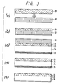
- Figs. 1(a) to (e) are process views for explaining one example of the method of preparing a semiconductor substrate of the present invention, each shown as a schematic cross-sectional view in each process.
- micro-pores of an average diameter of about 600 ⁇ are formed in the porous Si layer, so that the density of the layer has been reduced half or below that of the monocrystalline Si. Nevertheless, the monocrystallinity is still maintained, so that it is possible to form a monocrystalline Si layer on the porous layer by epitaxial growth.
- the temperature exceeds 1000°C, rearrangement of internal pores occurs, which impedes the acceleration of the etching.
- the epitaxial growth of the Si layer is preferably effected by a low-temperature growth method such as, for example, a molecular beam epitaxial growth method, a CVD method such as plasma CVD method, low-pressure CVD or photo CVD method, a bias sputter method, or a liquid-phase growth method.
- a low-temperature growth method such as, for example, a molecular beam epitaxial growth method, a CVD method such as plasma CVD method, low-pressure CVD or photo CVD method, a bias sputter method, or a liquid-phase growth method.
- a P-type Si monocrystalline substrate 11 is prepared and made entirely porous, as shown in Fig. 1(a).
- the epitaxial growth is made on the surface of a porous substrate 12, with one of various growth methods, as shown in Fig. 1(b), to form a thin film monocrystalline layer 13.
- the P-type Si substrate is made porous by anodization using an HF solution.
- the density of the porous Si layer can be changed to the range of 1.1 to 0.6 g/cm3 by changing the concentration of the HF solution from 50 to 20%, as compared with the density of 2.33 g/cm3 of monocrystalline Si.
- This porous layer is not formed on the N-type Si layer, owing to the following reasons, but only on the P-type Si substrate.
- the porous Si layer has pores having an average size of about 600 ⁇ which was measured by observation with a transmission electron microscope.
- Porous Si was discovered in the course of research on electrolytic polishing of a semiconductor which was conducted by Uhlir et al., in 1956 (A. Uhlir, Bell Syst. Tech. J., vol. 35, 333 (1956)).
- Unagami et al. investigated dissolving reaction of Si during anodization and reported that the anodic reaction of Si in an HF solution requires positive holes, and that the reaction is expressed as follows (T. Unagami, J. Electrochem. soc., vol. 127, 476 (1980)).
- e+ and e ⁇ respectively denote a positive hole and an electron
- n and ⁇ each denote the number of positive holes required for dissolving one silicon atom.
- Porous Si can be formed when the condition, n > 2 or ⁇ > 4, is satisfied.
- the P-type Si having positive holes can be made porous, while the N-type Si cannot be made porous.
- the selectivity in producing a porous structure has been demonstrated by Nagano et al. and Imai (Nagano, Nakajima, Yasumo, Oonaka, Kajiwara, Electronic Communications Institute Technical Studies Report, vol. 79, SSD79-9549 (1979)), (K. Imai, Solid-State Electronics, vol. 24, 159 (1981)).
- N-type Si can be made porous (R. P. Holmstrom and J. K. Chi, Appl. Phys. Lett., vol. 42, 386 (1983)), so that it is important to select a substrate which can be made porous irrespectively of whether it is P-type or N-type.
- Porous layer is internally formed with a large amount of gaps, resulting in the density decreasing to half or less. Consequently, the surface area will drastically increase as compared with that of deposition, so that its chemical etching rate is remarkably higher than that of the normal monocrystalline layer.
- a light-transparent substrate 14 which is typically a glass sheet, is prepared as an insulating substrate, and bonded on the surface of monocrystalline Si layer 13, to a degree of pulling against each other with a Van der Waals force (primary bonding). It will be appreciated that after an oxide layer is formed on the surface of Si monocrystalline layer 13, the oxide layer and the light-transparent substrate 14 may be bonded. Also, it will be appreciated that in place of the light-transparent substrate 14, a substrate having an oxide layer formed on the surface of monocrystalline Si may be used. The bonding strength of the primary bonding must be strong enough to retain the primary bonding state, without yielding exfoliations in the course to the secondary bonding to be performed later.
- the primary bonding can be performed at room temperature, or by heating, but when heating, the heating temperature must be lower than the temperatue used for the secondary bonding.
- the temperature for the secondary bonding is suitably in a range of 200 to 800°C, depending on the material of insulating substrate.
- the porous Si substrate 12 is entirely etched, whereby a thinned monocrystalline Si layer 13 is left on the light transparent substrate 14, as shown in Fig. 1(d).
- an anti-etching film must be provided on the back surface of the light-transparent glass substrate 14, except for an instance where the light-transparent glass substrate 14 is etched more or less, but the etched surface is not different from an optically polished surface, and an instance where the light-transparent glass substrate 14 is not etched at all.
- An Si3N4 layer is formed by deposition as the anti-etching film to cover wholly the two adjacently placed substrates, and the Si3N4 layer on the porous Si substrate is removed. It is possible to use other materials such as Apiezon wax, in place of Si3N4, as the material of the anti-etching layer.
- Si/SiO2 layer and light-transparent substrate 14 are bonded more strongly for the secondary bonding. Since the thin film and the light-transparent substrate are bonded as above described, the thin film is bonded in alignment with the substrate, so that it is possible to prevent exfoliations and cracks of the substrate caused by the difference between their thermal expansion coefficients.
- Fig. 1(e) shows the semiconductor substrate obtained by this embodiment, in which a monocrystalline Si layer 13 having a crystallinity equivalent to that of a silicon wafer is formed on the light-transparent substrate 14, with high degrees of smoothness and uniformity, and with a small thickness, over a wide area covering the whole surface of the wafer.
- the semiconductor substrate thus obtained is advantageous from the view point of production of an insulation-isolated electronic device.
- Figs. 2(a) to (e) are process views for explaining another example of the method of preparing a semiconductor substrate of the present invention, each shown as a schematic cross-sectional view in each process.
- a low-carrier density layer 22 is formed by epitaxial growth with one of various thin film growth methods or by counter doping the surface of a high-carrier density Si substrate 21, as shown in Fig. 2(a).
- an N-type monocrystalline layer 22 may be formed on the surface of a P-type Si moncrystalline substrate 21 by ion implantation of protons.
- the P-type or high-density N-type Si monocrystalline substrate 21 is changed into a porous Si substrate 23 by effecting, on the reverse side thereof, anodization using an HF solution.
- the initial monocrystalline Si having the density of 2.33 g/cm3 can be changed into a porous member the density of which can be varied within the range between 1.1 and 0.6 g/cm3 by varying the HF concentration of the etching solution between 50% and 20%.
- This porous member is formed into a P-type or high-density N-type Si substrate, as above described.
- a light-transparent substrate 24 which is typically a glass sheet, is prepared as an insulating substrate, and bonded on the surface of Si monocrystalline layer 22, to a degree of pulling against each other with a Van der Waals force (primary bonding). It will be appreciated that after an oxide layer is formed on the surface of Si monocrystalline layer 22, the oxide layer and the light-transparent substrate 24 may be bonded. Also, it will be appreciated that in place of the light-transparent substrate 24, a substrate having an oxide layer formed on the surface of monocrystalline Si may be used.
- the bonding strength of the primary bonding must be strong enough to retain the primary bonding state, without yielding exfoliations in the course to the secondary bonding to be performed later.
- the porous Si substrate 23 is entirely etched, whereby a thinned monocrystalline Si layer 22 is left on the light-transparent substrate 24, as shown in Fig. 2(d).
- the etching solution may also etch the light-transparent glass substrate 24 in etching, an anti-etching film must be provided on the back surface of the light-transparent glass substrate 24, except for an instance where the light-transparent glass substrate 24 is etched more or less, but the etched surface is not different from an original optically polished surface, and an instance where the light-transparent glass substrate 24 is not etched at all.
- An Si3N4 layer is formed by deposition as the anti-etching film to cover the entire member composed of the two substrates bonded together, and the Si3N4 layer on the surface of porous Si substrate is removed. It is possible to use other materials such as Apiezon wax, in place of Si3N4, as the material of the anti-etching layer.
- Si/SiO2 layer and light-transparent substrate 14 are bonded more strongly for the secondary bonding, as shown in Fig. 2(e). Since the thin film and the light-transparent substrate are bonded as above described, the thin film is bonded in alignment with the substrate, so that it is possible to prevent exfoliations and cracks of the substrate caused by the difference between their thermal expansion coefficients.
- Fig. 2(e) shows the semiconductor substrate obtained by this embodiment, in which a monocrystalline Si layer 22 having a crystallinity equivalent to that of a silicon wafer is formed on the light-transparent substrate 24, with high degrees of smoothness and uniformity, and with a small thickness, over a wide area covering the whole surface of the wafer.
- the semiconductor substrate thus obtained is advantageous from the view point of production of an insulation-isolated electronic device.
- the above method is one in which an apitaxial layer is formed before making a porous structure, and then the regions other than the epitaxial layer are made porous selectively by anodization.
- Figs. 3(a) to (d) are process views for explaining this embodiment, each shown as a schematic cross-sectional view in each process.
- an Si monocrystalline semiconductor member 31 of P-type is prepared, and is wholly changed into porous structure 32.
- an epitaxial growth is effected by a suitable method on the surface of the porous member 32, thereby forming a monocrystalline Si layer 33.
- the surface of the monocrystalline Si layer 33 on the porous Si substrate 32 is oxidized to form an oxide film 35.
- This oxide film 35 is formed to reduce the interface level of the monocrystalline layer 33 which is a final active layer.
- an insulating substrate 34 such as a light-transparent glass substrate is bonded on the surface of the oxide film 35, to a degree of pulling against each other with a Van der Waals force, or to a degree that bonded interfaces may not exfoliate due to a difference between thermal expansion coefficients of both members (primary bonding).
- this insulating substrate 34 may be, in place of the glass substrate, a substrate having an oxide layer formed on the surface of monocrystalline Si.
- the bonding strength of the primary bonding must be strong enough to retain the primary bonding state, without yielding exfoliations in the course to the secondary bonding for the complete bonding to be performed later.
- an anti-etching film 36 is provided on the back surface of the light-transparent glass substrate 34.
- An Si3N4 layer is formed by deposition as the anti-etching film 36 to cover the entire member composed of the two substrates bonded together, and the Si3N4 layer on the surface of porous Si substrate is removed. It is possible to use other materials such as Apiezon wax, in place of Si3N4, as the material of the anti-etching layer.
- the porous Si substrate 32 is entirely immersed in hydrofluoric acid with agitating so that only the porous Si is removed by electroless wet chemical etching, whereby a thinned monocrystalline silicon layer 13 is left on the light-transparent substrate 34.
- Si/SiO2 layer and light-transparent substrate 14 are bonded more strongly for the secondary bonding which is a complete bonding, as shown in Fig. 1(e), so that a semiconductor member of this embodiment can be obtained by removing the anti-etching film 36.
- Fig. 5 shows the etching time dependency of etched thickness of porous Si and monocrystalline Si when the porous Si and the monocrystalline Si are etched by being immersed in 49% hydrofluoric acid and agitated.
- the porous Si was formed by anodizing a monocrystalline Si.
- the conditions of anodization are shown below. It is to be noted, however, that the starting material for producing porous Si by anodization is not limited to monocrystalline Si and Si of other crystalline structure may be used as the starting material.
- Test pieces of the porous Si thus prepared were immersed in 49% hydrofluoric acid solution (white circles) at the room temperature and agitated. The reduction in the thickness of the porous Si was then measured.
- the porous Si was rapidly etched: namely, by a layer thickness of 90 ⁇ m in 40 minutes, and further 205 ⁇ m in 80 minutes, with high degrees of surface quality and uniformity.
- the etching rate has dependencies on the concentration of the etching solution and the temperature.
- Test pieces of non-porous Si having a thickness of 500 ⁇ m were immersed in 49% hydrofluoric acid solution (black circles) at the room temperature and agitated. The reduction in the thickness of the non-porous Si was then measured. The non-porous Si was only etched to 50 ⁇ or less after elapse of 120 minutes.
- the etched test pieces of porous Si and non-porous Si were then rinsed with water and the surfaces after the rinsing were examined by microanalysis using secondary ions but no impurity was detected.
- the conditions for the solution concentration and the temperature were set in the range where the etching rate of porous Si and the selection ratio of etching the porous Si and the non-porous Si have no effect in the practical use such as a fabrication process.
- etching of Si proceeds as follows: Si + 2O ⁇ Si O2 SiO2 + 4HF ⁇ SiF4 + H2O
- Si is oxidized by nitric acid to SiO2, and the SiO2 produced is etched with hydrofluoric acid.
- etching solutions for non-porous Si include the above fluoronitric acid-type etching solution as well as ethylenediamine-type, KOH-type and hydrazine-type etching solutions and the like.
- porous Si is conventionally selectively etched by the method which uses an aqueous NaOH solution as an etching solution.
- the porous Si is etched with the fluoronitric acid-type etching solution, but monocrystalline Si may be possibly etched.
- the etching solution is hydrofluoric acid, which has no etching action on the non-porous Si, but is used in an ordinary semiconductor process, with quite less etching contamination.
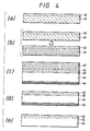
- Figs. 4(a) to (e) are process views for explaining this embodiment, each shown as a schematic cross-sectional view in each process.
- a low-carrier density layer 42 is formed by epitaxial growth with one of various thin film growth methods or by counter doping the surface of a high-carrier density Si substrate 41, as shown in Fig. 4(a).
- an N-type monocrystalline layer 42 may be formed on the surface of a P-type Si monocrystalline substrate 41 by ion implantation of protons.
- the P-type or high-density N-type Si monocrystalline substrate 41 is changed into a porous Si substrate 43 by effecting, on the reverse side thereof, anodization using an HF solution.
- the initial monocrystalline Si having the density of 2.33 g/cm3 can be changed into a porous member the density of which can be varied within the range between 1.1 and 0.6 g/cm3 by varying the HF concentration of the etching solution between 50% and 20%.
- This porous member is formed into a P-type or high-density N-type Si substrate, as above described.
- a light-transparent substrate 44 which is typically a glass sheet, is prepared as an insulating substrate, and after oxidizing the surface of monocrystalline Si layer on a porous Si substrate, bonded on the oxidized surface at the room temperature or by heating, to a degree of pulling against each other with a Van der Waals force or to a degree that the bonded interfaces may not exfoliate due to a difference between thermal expansion coefficients of both members (primary bonding).
- a substrate having an oxide layer formed on the surface of monocrystalline Si may be used.
- the bonding strength of the primary bonding must be strong enough to retain the primary bonding state, without yielding exfoliations in the course to the secondary bonding for the complete bonding to be performed later.
- the oxide layer 45 on the surface of monocrystalline layer is formed to reduce the interface level of the monocrystalline layer 42 which is a final active layer.
- an anti-etching film 46 is provided on the back surface of the light-transparent glass substrate 44.
- An Si3N4 layer is formed by deposition as the anti-etching film to cover the entire member composed of the two substrates bonded together, and the Si3N4 layer on the surface of porous Si substrate is removed. It is possible to use other materials such as Apiezon wax, in place of Si3N4, as the material of the anti-etching layer.
- the porous Si substrate 43 is entirely immersed in hydrofluoric acid, with agitating so that only the porous Si is etched by electroless wet chemical etching, whereby a thinned monocrystalline Si layer 42 is left on the light-transparent substrate 44.
- Si/SiO2 layer and light-transparent substrate 44 are bonded completely in the secondary bonding.
- the thin film and the light-transparent substrate are bonded as above described, the thin film is bonded in alignment with the substrate, so that it is possible to prevent exfoliations and cracks of the substrate caused by the difference between their thermal expansion coefficients.
- Fig. 4(e) shows the semiconductor substrate obtained by this embodiment, in which a monocrystalline Si layer 42 having a crystallinity equivalent to that of a silicon wafer is formed on the light-transparent substrate 44, with high degrees of smoothness and uniformity, and with a small thickness, over a wide area covering the whole surface of the wafer.
- the semiconductor substrate thus obtained is advantageous from the view point of production of an insulation-isolated electronic device.
- the conditions for the solution concentration and the temperature were set in the range where the etching rate of porous Si and the selection ratio of etching the porous Si and the non-porous Si have no effect in the practical use such as a fabrication process.
- the above method is one in which an epitaxial layer is formed before making a porous structure, and then the regions other than the epitaxial layer are made porous selectively by anodization.
- the etching rate has dependencies on the concentration of the etching solution and the temperature.
- the etching solution concentration and temperature are suitably determined in practical ranges. In the embodiments 2-1 and 2-2, 49% hydrofluoric acid and the room temperature are used, but the present invention is not limited to such conditions.
- the concentration of the hydrofluoric acid is 5% to 95%, and the temperature is set to a level which is ordinarily adopted.
- the etching can be made using a mixture liquid of hydrofluoric acid and alcohol, in place of hydrofluoric acid used for an etching solution in embodiments 2-1 and 2-2.
- porous Si can be selectively etched with high degrees of efficiency and uniformity, without etching non-porous Si, as in the embodiments 2-1 and 2-2.
- Fig. 6 shows the time dependency of etching thickness of porous Si and monocrystalline Si as observed when the porous Si and the monocrystalline Si are etched by being immersed in the mixture liquid (10:1) of 49% hydrofluoric acid and alcohol without agitation of the liquid.
- the porous Si was formed by anodizing the monocrystalline Si.
- the conditions of anodization are shown below. It is to be noted, however, that the starting material for producing porous Si by anodization is not limited to monocrystalline Si and Si of other crystalline structure may be used as the starting material.
- Test pieces of the porous Si prepared as described above were immersed, without agitation, in a mixture solution (10:1) of 49% hydrofluoric acid and alcohol (white circles). The reduction in the thickness of the porous Si was then measured.
- the porous Si was rapidly etched: namely, by a layer thickness of 85 ⁇ m in 40 minutes, and further 195 ⁇ m in 80 minutes, with high degrees of surface quality and uniformity.
- the etching rate has dependencies on the concentration of the etching solution and the temperature.
- Test pieces of non-porous Si having a thickness of 500 ⁇ m were immersed in a mixture liquid (10:1) of 49% hydrofluoric acid and alcohol (black circles) at the room temperature without agitation. The reduction in the thickness of the non-porous Si was then measured. The non-porous Si was only etched to 50 ⁇ or less after elapse of 120 minutes.
- the addition of alcohol serves to remove bubbles of reaction product gases generated as a result of the etching without delay from the surface being etched, without necessitating agitation, thus ensuring a high efficiency and uniformity of the etching.
- the etched test pieces of porous Si and non-porous Si were then rinsed with water and the surfaces after the rinsing were examined by microanalysis using secondary ions but no impurity was detected.
- the conditions for the concentration of etching solution and the temperature were set in the range where the etching rate has no effect in the practical use such as a fabrication process, and alcohol can exhibit its effects.
- the mixture solution (10:1) of 49% hydrofluoric acid and ethyl alcohol, as well as the room temperature as the solution temperature, are mentioned, the present invention is not limited to such conditions.
- the HF concentration with respect to the etching solution preferably ranges between 1 and 95%, more preferably between 5 and 90%, and most preferably between 5 and 80%.
- the alcohol concentration with respect to the etching solution is preferably 80% or less, more preferably 60% or less, and most preferably 40% or less, and is determined so as to provide an appreciable effect of alcohol.
- the temperature is set in a range of preferably 0 to 100°C, more preferably 5 to 80°C, and most preferably 5 to 60°C.
- ethyl alcohol has been used in this invention
- other alcohols such as isopropyl alcohol, which does not cause any inconvenience in the commercial production and which can provide an appreciable effect of addition of such alcohol, may be used as the alcohol.
- the etching can be made using a mixture liquid of hydrofluoric acid and hydrogen peroxide, in place of hydrofluoric acid used for an etching solution in embodiments 2-1 and 2-2.
- porous Si can be selectively etched with high degrees of efficiency and uniformity, without etching non-porous Si, as in the embodiments 2-1 and 2-2.
- Fig. 7 shows the time dependency of etching thickness of porous Si and monocrystalline Si as observed when the porous Si and the monocrystalline Si are etched by being immersed in a mixture liquid (1:5) of 49% hydrofluoric acid and 30% hydrogen peroxide and agitated.
- the porous Si was formed by anodizing the monocrystalline Si.
- the conditions of anodization are shown below. It is to be noted, however, that the starting material for producing porous Si by anodization is not limited to monocrystalline Si and Si of other crystalline structure may be used as the starting material.
- Test pieces of the porous Si prepared as described above were immersed, without agitation, in the mixture solution (1:5) of 49% hydrofluoric acid and 30% hydrogen peroxide (white circles) at the room temperature. The reduction in the thickness of the porous Si was then measured.
- the porous Si was rapidly etched: namely, by a layer thickness of 112 ⁇ m in 40 minutes, and further 256 ⁇ m in 80 minutes, with high degrees of surface quality and uniformity.
- the etching rate has dependencies on the concentration of the etching solution and the temperature.
- Test pieces of non-porous Si having a thickness of 500 ⁇ m were immersed in the mixture liquid (1:5) of 49% hydrofluoric acid and 30% hydrogen peroxide (black circles) at the room temperature and agitated. The reduction in the thickness of the non-porous Si was then measured. The non-porous Si was only etched to 50 ⁇ or less after elapse of 120 minutes.
- the addition of hydrogen peroxide serves to accelerate oxidation of silicon, thus enhancing the reaction speed as compared to the case where hydrogen peroxide is not added.
- the reaction speed can be controlled by suitably selecting the content of the hydrogen peroxide.
- the etched test pieces of porous Si and non-porous Si were then rinsed with water and the surfaces after the rinsing were examined by microanalysis using secondary ions but no impurity was detected.
- the etching rate has dependencies on the solution concentrations of hydrofluoric acid and hydrogen peroxide, as well as the temperature.
- the addition of hydrogen peroxide solution makes it possible to accelerate the oxidation of silicon, and the reaction speed as compared to the case when it is not added. Further, the reaction speed can be controlled by suitably selecting the content of the hydrogen peroxide.
- the conditions for the concentration of etching solution and the temperature can be set to fall within the ranges in which the effects of hydrofluoric acid and hydrogen peroxide solution can be exhibited and the etching rate would not cause any practical inconvenience in commercial production.
- the mixture solution (1:5) of 49% hydrofluoric acid and hydrogen peroxide, as well as the room temperature as the solution temperature, are mentioned as an instance, the present invention is not limited to such conditions.
- the HF concentration with respect to the etching solution preferably ranges between 1 and 95%, mote preferably between 5 and 90%, and most preferably between 5 and 80%.
- the H2O2 concentration with respect to the etching solution preferably ranges between 1 and 95%, more preferably between 5 and 90%, and most preferably between 10 and 80%, and is determined so as to provide an appreciable effect of hydrogen peroxide.
- the temperature is set in a range of preferably 0 to 100°C, more preferably 5 to 80°C, and most preferably 5 to 60°C.
- the etching can be made using a mixture liquid of hydrofluoric acid, alcohol and hydrogen peroxide, in place of hydrofluoric acid used for an etching solution in embodiments 2-1 and 2-2.
- porous Si can be selectively etched with high degrees of efficiency and uniformity, without etching non-porous Si, as in the embodiments 2-1 and 2-2.
- Fig. 8 shows the time dependency of etching thickness of porous Si and monocrystalline Si as observed when the porous Si and the monocrystalline Si are etched by being immersed in a mixture liquid (10:6:50) of 49% hydrofluoric acid, alcohol and 30% hydrogen peroxide without agitation.
- the porous Si was formed by anodizing the monocrystalline Si.
- the conditions of anodization are shown below. It is to be noted, however, that the starting material for producing porous Si by anodization is not limited to monocrystalline Si and Si of other crystalline structure may be used as the starting material.
- Test pieces of the porous Si prepared as described above were immersed, without agitation, in the mixture solution (10:6:5) of 49% hydrofluoric acid, alcohol and 30% hydrogen peroxide (white circles) at the room temperature. The reduction in the thickness of the porous Si was then measured.
- the porous Si was rapidly etched: namely, by a layer thickness of 107 ⁇ m in 40 minutes, and further 244 ⁇ m in 80 minutes, with high degrees of surface quality and uniformity.
- the etching rate has dependencies on the concentration of the etching solution and the temperature.
- Test pieces of non-porous Si having a thickness of 500 ⁇ m were immersed in the mixture liquid (10:6:5) of 49% hydrofluoric acid, alcohol and 30% hydrogen peroxide (black circles) at the room temperature without agitation. The reduction in the thickness of the non-porous Si was then measured. The non-porous Si was only etched to 50 ⁇ or less after elapse of 120 minutes.
- the etched test pieces of porous Si and non-porous Si were then rinsed with water and the surfaces after the rinsing were examined by microanalysis using secondary ions but no impurity was detected.
- the etching rate has dependencies on the solution concentrations of hydrofluoric acid and hydrogen peroxide, as well as the temperature.
- the addition of hydrogen peroxide solution makes it possible to accelerate the oxidation of silicon, and the reaction speed as compared to the case when it is not added. Further, the reaction speed can be controlled by suitably selecting the content of the hydrogen peroxide.
- the addition of alcohol serves to remove bubbles of reaction product gases generated as a result of the etching without delay from the surface being etched, without necessitating agitation, thus ensuring a high efficiency and uniformity of the etching for the porous Si.
- the conditions for the concentration of etching solution and the temperature can be set to fall within the ranges in which the effects of hydrofluoric acid, hydrogen peroxide solution and alcohol can be exhibited and the etching rate would not cause any practical inconvenience in commercial production.
- the mixture solution (10:6:5) of 49% hydrofluoric acid, ethyl alcohol and hydrogen peroxide, as well as the room temperature as the solution temperature, are mentioned as an instance, the present invention is not limited to such conditions.
- the HF concentration with respect to the etching solution preferably ranges between 1 and 95%, more preferably between 5 and 90%, and most preferably between 5 and 80%.
- the H2O2 concentration with respect to the etching solution preferably ranges between 1 and 95%, more preferably between 5 and 90%, and most preferably between 10 and 80%, and is determined so as to provide an appreciable effect of hydrogen peroxide.
- the alcohol concentration with respect to the etching solution is preferably 80% or less, more preferably 60% or less, and most preferably 40% or less, and is determined so as to provide an appreciable effect of alcohol.
- the temperature is set in a range of preferably 0 to 100°C, more preferably 5 to 80°C, and most preferably 5 to 60°C.
- ethyl alcohol has been specifically used in this invention, other alcohols such as isopropyl alcohol, which does not cause any inconvenience in the commercial production and which can provide an appreciable effect of addition of such alcohol, may be used as the alcohol.
- the etching can be made using a buffered hydrofluoric acid, in place of hydrofluoric acid used for an etching solution in embodiments 2-1 and 2-2.
- porous Si can be selectively etched with high degrees of efficiency and uniformity, without etching non-porous Si, as in the embodiments 2-1 and 2-2.
- Fig. 9 shows the time dependency of etching thickness of porous Si and monocrystalline Si as observed when the porous Si and the monocrystalline Si are etched by being immersed in buffered hydrofluoric acid (a mixture solution of 4.5% hydrofluoric acid and 36% ammonium fluoride) and agitated.
- buffered hydrofluoric acid a mixture solution of 4.5% hydrofluoric acid and 36% ammonium fluoride
- the porous Si was formed by anodizing the monocrystalline Si.
- the conditions of anodization are shown below. It is to be noted, however, that the starting material for producing porous Si by anodization is not limited to monocrystalline Si and Si of other crystalline structure may be used as the starting material.
- Test pieces of the porous Si prepared as described above were immersed, without agitation, in the buffered hydrofluoric acid (a mixture solution of 4.5% hydrofluoric acid and 36% ammonium fluoride) (white circles) at the room temperature. The reduction in the thickness of the porous Si was then measured.
- the porous Si was rapidly etched: namely, by a layer thickness of 70 ⁇ m in 40 minutes, and further 118 ⁇ m in 120 minutes, with high degrees of surface quality and uniformity.
- the etching rate has dependencies on the concentration of the etching solution and the temperature.
- Test pieces of non-porous Si having a thickness of 500 ⁇ m were immersed in the buffered hydrofluoric acid (a mixture solution of 4.5% hydrofluoric acid and 36% ammonium fluoride) (black circles) at the room temperature and agitated. The reduction in the thickness of the non-porous Si was then measured. The non-porous Si was only etched to 50 ⁇ or less after elapse of 120 minutes.
- buffered hydrofluoric acid a mixture solution of 4.5% hydrofluoric acid and 36% ammonium fluoride
- the etched test pieces of porous Si and non-porous Si were then rinsed with water and the surfaces after the rinsing were examined by microanalysis using secondary ions but no impurity was detected.
- the buffered hydrofluoric acid is a mixture solution of 36% ammonium fluoride (NH4F) and 4.5% hydrogen fluoride.
- the etching rate has dependencies on the solution concentrations, as well as the temperature.
- the conditions for the concentration of etching solution and the temperaure can be set to fall within the ranges in which no practical inconvenience would not be caused in commercial production.
- the buffered hydrofluoric acid containing a solution of 36% ammonium fluoride (NH4F) and 4.5% hydrogen fluoride (HF), as well as the room temperature as the solution temperature are mentioned as an instance, the present invention is not limited to such conditions.
- the HF concentration in the buffered hydrofluoric acid with respect to the etching solution preferably ranges between 1 and 95%, more preferably between 1 and 85%, and most preferably between 1 and 70%.
- the NH4F concentration in the buffered hydrofluoric acid with respect to the etching solution preferably ranges between 1 and 95%, more preferably between 5 and 90%, and most preferably between 5 and 80%.
- the temperature is set in a range of preferably 0 to 100°C, more preferably 5 to 80°C, and most preferably 5 to 60°C.
- the etching can be made using a mixture solution of buffered hydrofluoric acid and alcohol, in place of hydrofluoric acid used for an etching solution in embodiments 2-1 and 2-2.
- porous Si can be selectively etched with high degrees of efficiency and uniformity, without etching non-porous Si, as in the embodiments 2-1 and 2-2.
- Fig. 10 shows the time dependency of etching thickness of porous Si and monocrystalline Si as observed when the porous Si and the monocrystalline Si are etched by being immersed in the mixture solution (10:1) of buffered hydrofluoric acid (a mixture solution of 4.5% hydrofluoric acid and 36% ammonium fluoride) and alcohol without agitation.
- buffered hydrofluoric acid a mixture solution of 4.5% hydrofluoric acid and 36% ammonium fluoride
- the porous Si was formed by anodizing the monocrystalline Si.
- the conditions of anodization are shown below. It is to be noted, however, that the starting material for producing porous Si by anodization is not limited to monocrystalline Si and Si of other crystalline structure may be used as the starting material.
- Test pieces of the porous Si prepared as described above were immersed, without agitation, in the mixture solution (10:1) of buffered hydrofluoric acid (a mixture solution of 4.5% hydrofluoric acid and 36% ammonium fluoride) and alcohol (white circles) at the room temperature. The reduction in the thickness of the porous Si was then measured.
- the porous Si was rapidly etched: namely, by a layer thickness of 83 ⁇ m in 40 minutes, and further 140 ⁇ m in 120 minutes, with high degrees of surface quality and uniformity.
- the etching rate has dependencies on the concentration of the etching solution and the temperature.
- Test pieces of non-porous Si having a thickness of 500 ⁇ m were immersed in the mixture solution of buffered hydrofluoric acid (a mixture solution of 4.5% hydrofluoric acid and 36% ammonium fluoride) and alcohol (black circles) at the room temperature without agitation. The reduction in the thickness of the non-porous Si was then measured. The non-porous Si was only etched to 50 ⁇ or less after elapse of 120 minutes.
- buffered hydrofluoric acid a mixture solution of 4.5% hydrofluoric acid and 36% ammonium fluoride
- the etched test pieces of porous Si and non-porous Si were then rinsed with water and the surfaces after the rinsing were examined by microanalysis using secondary ions but no impurity was detected.
- the etching rate has dependencies on the solution concentrations of buffered hydrofluoric acid, as well as the temperature.
- the addition of alcohol serves to remove bubbles of reaction product gases generated as a result of the etching without delay from the surface being etched, without necessitating agitation, thus ensuring a high efficiency and uniformity of the etching for the porous Si.
- the conditions for the concentration of etching solution and the temperature can be set to fall within the ranges in which the etching rate would cause no practical inconvenience in commercial production, with an appreciable effect of alcohol.
- the mixture solution (10:1) of buffered hydrofluoric acid (a mixture solution of 4.5% hydrogen fluoride and 36% ammonium fluoride) and ethyl alcohol, as well as the room temperature as the solution temperature, are mentioned as an instance, the present invention is not limited to such conditions.
- the HF concentration in the buffered hydrofluoric acid with respect to the etching solution preferably ranges between 1 and 95%, more preferably between 1 and 85%, and most preferably between 1 and 70%.
- the ammonium fluoride (NH4F) concentration in the buffered hydrofluoric acid with respect to the etching solution preferably ranges between 1 and 95%, more preferably between 5 and 90%, and most preferably between 5 and 80%.
- the alcohol concentration with respect to the etching solution is preferably 80% or less, more preferably 60% or less, and most preferably 40% or less, and is determined so as to provide an appreciable effect of alcohol.
- the temperature is set in a range of preferably 0 to 100°C, more preferably 5 to 80°C, and most preferably 5 to 60°C.
- ethyl alcohol has been specifically used in this invention, other alcohols such as isopropyl alcohol, which does not cause any inconvenience in the commercial production and which can provide an appreciable effect of addition of such alcohol, may be used as the alcohol.
- the etching can be made using a mixture solution of buffered hydrofluoric acid and hydrogen peroxide, in place of hydrofluoric acid used for an etching solution in embodiments 2-1 and 2-2.
- porous Si can be selectively etched with high degrees of efficiency and uniformity, without etching non-porous Si, as in the embodiments 2-1 and 2-2.
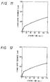
- Fig. 11 shows the time dependency of etching thickness of porous Si and monocrystalline Si as observed when the porous Si and the monocrystalline Si are etched by being immersed in the mixture solution (1:5) of buffered hydrofluoric acid (a mixture solution of 4.5% hydrofluoric acid and 36% ammonium fluoride) and 30% hydrogen peroxide and agitated.
- buffered hydrofluoric acid a mixture solution of 4.5% hydrofluoric acid and 36% ammonium fluoride
- the porous Si was formed by anodizing the monocrystalline Si.
- the conditions of anodization are shown below. It is to be noted, however, that the starting material for producing porous Si by anodization is not limited to monocrystalline Si and Si of other crystalline structure may be used as the starting material.
- Test pieces of the porous Si prepared as described above were immersed, with agitation, in the mixture solution (1:5) of buffered hydrofluoric acid (a mixture solution of 4.5% hydrofluoric acid and 36% ammonium fluoride) and 30% hydrogen peroxide (white circles) at the room temperature.
- the reduction in the thickness of the porous Si was then measured.
- the porous Si was rapidly etched: namely, by a layer thickness of 88 ⁇ m in 40 minutes, and further 147 ⁇ m in 120 minutes, with high degrees of surface quality and uniformity.
- the etching rate has dependencies on the concentration of the etching solution and the temperature.
- Test pieces of non-porous Si having a thickness of 500 ⁇ m were immersed in the mixture solution (1:5) of buffered hydrofluoric acid (a mixture solution of 4.5% hydrofluoric acid and 36% ammonium fluoride) and 30% hydrogen peroxide (black circles) at the room temperature and agitated. The reduction in the thickness of the non-porous Si was then measured. The non-porous Si was only etched to 50 ⁇ or less after elapse of 120 minutes.
- buffered hydrofluoric acid a mixture solution of 4.5% hydrofluoric acid and 36% ammonium fluoride
- 30% hydrogen peroxide black circles
- the etched test pieces of porous Si and non-porous Si were then rinsed with water and the surfaces after the rinsing were examined by microanalysis using secondary ions but no impurity was detected.
- the etching rate has dependencies on the solution concentrations of buffered hydrofluoric acid and hydrogen peroxide, as well as the temperature.
- the addition of hydrogen peroxide solution makes it possible to accelerate the oxidation of silicon, and the reaction speed as compared to the case when it is not added. Further, the reaction speed can be controlled by suitably selecting the content of the hydrogen peroxide.
- the conditions for the concentration of etching solution and the temperature can be set to fall within the ranges in which they provide an appreciable effect of buffered hydrofluoric acid and hydrogen peroxide and the etching rate would cause no practical inconvenience in commercial production.
- the mixture solution (1:5) of buffered hydrofluoric acid and hydrogen peroxide, as well as the room temperature as the solution temperature, are mentioned as an instance, the present invention is not limited to such conditions.
- the HF concentration in the buffered hydrofluoric acid with respect to the etching solution preferably ranges between 1 and 95%, more preferably between 1 and 85%, and most preferably between 1 and 70%.
- the H2O2 concentration with respect to the etching solution preferably ranges between 1 and 95%, more preferably between 5 and 90%, and most preferably between 5 and 80%, and is determined so as to provide an appreciable effect of hydrogen peroxide.
- the temperature is set in a range of preferably 0 to 100°C, more preferably 5 to 80°C, and most preferably 5 to 60°C.
- the etching can be made using a mixture solution of buffered hydrofluoric acid, alcohol and hydrogen peroxide, in place of hydrofluoric acid used for an etching solution in embodiments 2-1 and 2-2.
- porous Si can be selectively etched with high degrees of efficiency and uniformity, without etching non-porous Si, as in the embodiments 2-1 and 2-2.
- Fig. 12 shows the time dependency of etching thickness of porous Si and monocrystalline Si as observed when the porous Si and the monocrystalline Si are etched by being immersed in the mixture solution (10:6:50) of buffered hydrofluoric acid (a mixture solution of 4.5% hydrofluoric acid and 36% ammonium fluoride), alcohol and 30% hydrogen peroxide without agitation.
- buffered hydrofluoric acid a mixture solution of 4.5% hydrofluoric acid and 36% ammonium fluoride
- the porous Si was formed by anodizing the monocrystalline Si.
- the conditions of anodization are shown below. It is to be noted, however, that the starting material for producing porous Si by anodization is not limited to monocrystalline Si and Si of other crystalline structure may be used as the starting material.
- Test pieces of the porous Si prepared as described above were immersed, without agitation, in the mixture solution (10:6:50) of buffered hydrofluoric acid (a mixture solution of 4.5% hydrofluoric acid and 36% ammonium fluoride), alcohol and 30% hydrogen peroxide (white circles) at the room temperature.
- the reduction in the thickness of the porous Si was then measured.
- the porous Si was rapidly etched: namely, by a layer thickness of 83 ⁇ m in 40 minutes, and further 140 ⁇ m in 120 minutes, with high degrees of surface quality and uniformity.
- the etching rate has dependencies on the concentration of the etching solution and the temperature.
- Test pieces of non-porous Si having a thickness of 500 ⁇ m were immersed in the mixture solution (10:6:50) of buffered hydrofluoric acid (a mixture solution of 4.5% hydrofluoric acid and 36% ammonium fluoride), alcohol and 30% hydrogen peroxide (black circles) at the room temperature without agitation. The reduction in the thickness of the non-porous Si was then measured. The non-porous Si was only etched to 50 ⁇ or less after elapse of 120 minutes.
- buffered hydrofluoric acid a mixture solution of 4.5% hydrofluoric acid and 36% ammonium fluoride
- alcohol 30% hydrogen peroxide
- the etched test pieces of porous Si and non-porous Si were then rinsed with water and the surfaces after the rinsing were examined by microanalysis using secondary ions but no impurity was detected.
- the etching rate has dependencies on the solution concentrations of hydrofluoric acid and hydrogen peroxide, as well as the temperature.
- the addition of hydrogen peroxide solution makes it possible to accelerate the oxidation of silicon, and the reaction speed as compared to the case when it is not added. Further, the reaction speed can be controlled by suitably selecting the content of the hydrogen peroxide.
- the addition of alcohol serves to remove bubbles of reaciton product gases generated as a result of the etching without delay from the surface being etched, without necessitating agitation, thus ensuring a high efficiency and uniformity of the etching for the porous Si.
- the conditions for the concentration of etching solution and the temperature can be set to fall within the ranges in which they provide an appreciable effect of buffered hydrofluoric acid, hydrogen peroxide and alcohol, and the etching rate would cause no practical inconvenience in commercial production.
- the mixture solution (10:6:50) of buffered hydrofluoric acid, ethyl alcohol and hydrogen peroxide, as well as the room temperature as the solution temperature are mentioned as an instance, the present invention is not limited to such conditions.
- the HF concentration in the buffered hydrofluoric acid with respect to the etching solution preferably ranges between 1 and 95%, more preferably between 5 and 90%, and most preferably between 5 and 80%.
- the H2O2 concentration with respect to the etching solution preferably ranges between 1 and 95%, more preferably between 5 and 90%, and most preferably between 10 and 80%, and is determined so as to provide an appreciable effect of hydrogen peroxide.
- the alcohol concentration with respect to the etching solution is preferably 80% or less, more preferably 60% or less, and most preferably 40% or less, and is determined so as to provide an appreciable effect of alcohol.
- the temperature is set in a range of preferably 0 to 100°C, more preferably 5 to 80°C, and most preferably 5 to 60°C.
- ethyl alcohol has been specifically used in this invention, other alcohols such as isopropyl alcohol, which does not cause any inconvenience in the commercial production and which can provide an appreciable effect of addition of such alcohol, may be used as the alcohol.
- Example 1 (example not forming an oxide layer)
- a 0.5 ⁇ m thick Si epitaxial layer 13 of 0.063 ⁇ cm was grown at a low temperature on the (100) porous Si substrate with MBE (Molecular Beam Epitaxy) method. Deposition was conducted under the following conditions (Fig. 1(b)).
- the etching speed of the porous layer is increased to about 100 times thereof, as previously described. That is, the porous Si substrate having a thickness of 200 ⁇ m was removed in 2 minutes with a result that the monocrystalline Si layer 13 having a thickness of 0.5 ⁇ m remained on the fused silica glass substrate 14. There was no change on the epitaxial layer 13.
- the back surface of the fused silica glass substrate 14 was etched 0.1 ⁇ m, but its front surface did not have any difference from its original optical polished face (Fig. 1(d)).
- a 0.5 ⁇ m thick Si epitaxial layer 13 of 0.063 ⁇ cm was grown at a low temperature on the (100) porous Si substrate with MBE (Molecular Beam Epitaxy) method. Deposition was conducted under the following conditions (Fig. 1(b)).
- this epitaxial layer was oxidized, and then an optically polished fused silica glass substrate 14 was placed on the surface of the oxidized film, and contacted thereto (Fig. 1(c)).
- the etching speed of the porous layer is increased to about 100 times thereof, as previously described. That is, the porous Si substrate having a thickness of 200 ⁇ m was removed in 2 minutes with a result that the monocrystalline Si layer 13 having a thickness of 0.5 ⁇ m remained on the fused silica glass substrate 14. There was no change on the epitaxial layer 13.
- the back surface of the fused silica glass substrate 14 was etched 0.1 ⁇ m, but its front surface did not have any difference from its original optical polished face (Fig. 1(d)).
- a 0.5 ⁇ m thick Si epitaxial layer was grown at a low temperature on the (100) porous Si substrate with plasma CVD method. Deposition was conducted under the following conditions (Fig. 1 (b)).
- this epitaxial layer was oxidized, and then an optically polished glass substrate having a softening point of about 500°C was placed on the surface of the oxidized film, and contacted thereto (Fig. 1 (c)).
- the etching speed of the normal Si monocrystal with a KOH 6M solution is about 1 ⁇ m or less per minute, but the etching speed of the porous layer is increased to about 100 times thereof, as previously described. That is, the 200 ⁇ m thick porous Si substrate was removed in 2 minutes with a result that the 0.5 ⁇ m thick monocrystalline Si layer remained on the glass substrate having a low softening point. There was no change on the epitaxial layer. (Fig. 1(d))
- a 1 ⁇ m thick Si epitaxial layer was grown at a low temperature on the (100) porous Si substrate with bias sputtering method. Deposition was conducted under the following conditions (Fig. 1(b)).
- this epitaxial layer was oxidized, and then an optically polished glass substrate having a softening point of about 500°C was placed on the surface of the oxidized film, and contacted thereto (Fig. 1(c)).
- the etching speed of the normal Si monocrystal with an NaOH 7M solution is about 1 ⁇ m or less per minute, but the etching speed of the porous layer is increased to about 100 times thereof, as previously described. That is, the 200 ⁇ m thick porous Si substrate was removed in 2 minutes with a result that the 1 ⁇ m thick monocrystalline Si layer remained on the glass substrate having a low softening point. There was no change on the epitaxial layer (Fig. 1(d)).
- a 0.5 ⁇ m thick Si epitaxial layer 13 of 0.063 ⁇ cm was grown at a low temperature on the (100) porous Si substrate with liquid phase growth method. Deposition was conducted under the following conditions.
- this epitaxial layer was oxidized, and then an optically polished glass substrate having a softening point of about 800°C was placed on the surface of the oxidized film, and contacted thereto.
- the etching speed of the porous layer is increased to about 100 times thereof, as previously described. That is, the porous Si substrate having a thickness of 200 ⁇ m was removed in 2 minutes with a result that the monocrystalline Si layer 13 having a thickness of 0.5 ⁇ m remained on the glass substrate. There was no change on the epitaxial layer.
- the back surface of the fused silica glass substrate was etched 0.1 ⁇ m, but its front surface did not have any difference from its original optical polished face.
- the SOI thin film layer and the glass substrate were firmly joined by heating them at 750°C for 0.5 hour in an oxygen atmosphere.
- a 0.5 ⁇ m thick Si epitaxial layer was grown at a low temperature on the (100) porous Si substrate with low-pressure CVD method. Deposition was conducted under the following conditions.
- this epitaxial layer was oxidized, and then an optically polished fused silica glass substrate was placed on the surface of the oxidized film, and contacted thereto.
- the etching speed of the normal Si monocrystal with a hydrofluoro-nitric acid solution is about 0.5 ⁇ m or less per minute.
- the etching speed of the porous layer is increased to about 100 times thereof, as previously described. That is, the porous Si substrate having a thickness of 200 ⁇ m was removed in 4 minutes with a result that the monocrystalline Si layer having a thickness of 0.5 ⁇ m remained on the fused silica glass substrate. There was no change on the epitaxial layer.
- the back surface of the fused silica glass substrate was hardly etched but its front surface did not have any difference from its original optical polished face.
- SiH2Cl2 was as a source gas, high-speed etching characteristics specific to the porous substrate were maintained, although the growth temperature must be elevated several tens degrees.
- the SOI thin film layer and the fused silica glass substrate were firmly joined by heating them at 800°C for 0.5 hour in a nitrogen atmosphere.
- Example 7 (example of not forming an oxide layer)
- a 1.0 ⁇ m thick Si epitaxial layer was grown on a P-type or N-type (100) monocrystalline Si substrate having a thickness of 200 ⁇ m and a specific resistance of 0.01 ⁇ cm by CVD method. Deposition was conducted under the following conditions:
- the etching speed of the porous layer is increased to about 100 times thereof, as previously described. That is, the porous Si substrate having a thickness of 200 ⁇ m was removed in 2 minutes with a result that the monocrystalline Si layer having a thickness of 1 ⁇ m remained on the fused silica glass substrate. There was no change on the epitaxial layer.
- the back surface of the fused silica glass substrate was etched 0.1 ⁇ m, but its front surface did not have any difference from its original optical polished face (Fig. 2(d)).
- a 1.0 ⁇ m thick Si epitaxial layer was grown on a P-type or N-type (100) monocrystalline Si substrate having a thickness of 200 ⁇ m and a specific resistance of 0.01 ⁇ cm by CVD method. Deposition was conducted under the following conditions:
- this epitaxial layer was oxidized, and then an optically polished fused silica glass substrate was placed on the surface of the oxide film, and contacted thereto (Fig. 2(c)).
- the etching speed of the porous layer is increased to about 100 times thereof, as previously described. That is, the porous Si substrate having a thickness of 200 ⁇ m was removed in 2 minutes with a result that the monocrystalline Si layer having a thickness of 1 ⁇ m remained on the fused silica glass substrate. There was no change on the epitaxial layer.
- the back surface of the fused silica glass substrate was etched 0.1 ⁇ m, but its front surface did not have any difference from its original optical polished face (Fig. 2(d)).
- a 0.5 ⁇ m thick Si epitaxial layer was grown on a P-type or high-density N-type (100) monocrystalline Si substrate having a thickness of 200 ⁇ m by CVD method. Deposition was conducted under the following conditions:
- this epitaxial layer was oxidized, and then an optically polished fused silica glass substrate was placed on the surface of the oxide film, and contacted thereto.
- the etching speed of the normal Si monocrystal with a hydrofluoro-nitric acid solution is about 0.5 ⁇ m or less per minute.
- the etching speed of the porous layer is increased to about 100 times thereof, as previously described. That is, the porous Si substrate having a thickness of 200 ⁇ m was removed in 4 minutes with a result that the monocrystalline Si layer having a thickness of 0.5 ⁇ m remained on the fused silica glass substrate. There was no change on the epitaxial layer.
- the back surface of the fused silica glass substrate was hardly etched but its front surface did not have any difference from its original optical polished face.
- the SOI thin film layer and the fused silica glass substrate were firmly joined by heating them at 800°C for 0.5 hour in a nitrogen atmosphere.
- a 0.5 ⁇ m thick Si epitaxial layer was grown on a P-type or high-density N-type (100) monocrystalline Si substrate having a thickness of 200 ⁇ m by MBE method. Deposition was conducted under the following conditions:
- this epitaxial layer was oxidized, and then an optically polished glass substrate having a softening point of about 800°C was placed on the surface of the oxide film, and contacted thereto.
- the etching speed of the normal Si monocrystal with a hydrofluoro-nitric acid solution is about 0.5 ⁇ m or less per minute.
- the etching speed of the porous layer is increased to about 100 times thereof, as previously described. That is, the porous Si substrate having a thickness of 200 ⁇ m was removed in 4 minutes with a result that the monocrystalline Si layer having a thickness of 0.5 ⁇ m remained on the fused silica glass substrate. There was no change on the epitaxial layer. The back surface of the glass substrate was hardly etched but its front surface did not have any difference from its original optical polished face.
- the SOI thin film layer and the glass substrate were firmly joined by heating them at 750°C for 0.5 hour in an oxygen atmosphere.
- a 1 ⁇ m thick N-type Si layer was formed on the surface of a P-type (100) monocrystal Si substrate having a thickness of 200 ⁇ m and a specific resistance of 0.01 ⁇ cm by proton implantation.
- Implantation rate of H+ was 5x10¹⁵ (ions/cm2).
- Anodization was conducted on this substrate in a 50% HF solution. At this time, the current density was 100 mA/cm2.
- the porous structure formation rate was 8.4 ⁇ m/min and hence it took twenty four minutes for the P-type (100) Si substrate having a thickness of 200 ⁇ m to be made entirely porous. As mentioned above, this anodization made only the P-type (100) Si substrate porous, and there was no change in the N-type Si layer.
- this epitaxial layer was oxidized, and then an optically polished fused silica glass substrate was placed on the surface of the oxide film, and contacted thereto.
- the etching speed of the porous layer is increased to about 100 times thereof, as previously described. That is, the porous Si substrate having a thickness of 200 ⁇ m was removed in 2 minutes with a result that the monocrystalline Si layer having a thickness of 1 ⁇ m remained on the fused silica glass substrate. There was no change on the epitaxial layer.
- the back surface of the fused silica glass substrate was etched 0.1 ⁇ m but its front surface did not have any difference from its original optical polished face.
- the SOI thin film layer and the fused silica glass substrate were firmly joined by heating them at 800°C for 0.5 hour in an oxygen atmosphere.
- a 1 ⁇ m thick high resistive Si layer having a specific resistance of 0.063 ⁇ cm was formed on the surface of a P-type (100) monocrystal Si substrate having a thickness of 200 ⁇ m and a specific resistance of 0.01 ⁇ cm by ion implantation of P+ (phosphorous ion). Implantation rate of P+ was 5x10¹⁵ (ions/cm2 ). Anodization was conducted on this substrate in a 50% HF solution. At this time, the current density was 100 mA/cm2. The porous structure formation rate was 8.4 ⁇ m/min and hence it took twenty four minutes for the low resistive P-type (100) Si substrate having a thickness of 200 ⁇ m to be made entirely porous. As mentioned above, this anodization made only the low resistive P-type (100) Si substrate porous, and there was no change in the high resistive Si layer.
- this epitaxial layer was oxidized, and then an optically polished fused silica glass substrate was placed on the surface of the oxide film, and contacted thereto.
- the etching speed of the porous layer is increased to about 100 times thereof, as previously described. That is, the porous Si substrate having a thickness of 200 ⁇ m was removed in 2 minutes with a result that the monocrystalline Si layer having a thickness of 1 ⁇ m remained on the fused silica glass substrate. There was no change on the epitaxial layer.
- the back surface of the fused silica glass substrate was etched 0.1 ⁇ m but its front surface did not have any difference from its original optical polished face.
- the SOI thin film layer and the fused silica glass substrate were firmly joined by heating them at 800°C for 0.5 hour in an oxygen atmosphere.
- anodization was conducted on a P-type or N-type (100) monocrystalline Si substrate having a thickness of 200 ⁇ m and a specific resistance of 0.01 ⁇ cm in an HF solution to make the substrate porous.
- the conditions of anodization are as follows.
- a 0.5 ⁇ m thick Si epitaxial layer (non-porous Si monocrystalline layer) of 0.063 ⁇ cm was grown at a low temperature on the (100) porous Si substrate by MBE (Molecular Beam Epitaxy) method. Deposition was conducted under the following conditions.
- this epitaxial layer was oxidized 1000 ⁇ , and then an optically polished fused silica glass substrate was placed on the surface of the oxide film, and contacted thereto, (primary bonding).
- the fused silica glass substrate was only covered with Si3N4 excellent in the chemical etching resistance.
- the etching rate of the non-porous Si monocrystal with the etching solution was so low that only a maximum of 50 ⁇ of non-porous monocrystalline Si was removed in seventy eight minutes. Since the ratio of the etching rate of the non-porous monocrystalline Si to that of the porous layer is 1:105, the amount of non-porous layer which is etched (several tens angstroms) can be ignored in a practical operation.
- the 200 ⁇ m-thick porous Si substrate was removed with a result that the 0.5 ⁇ m-thick monocrystalline Si layer remained on the fused silica glass substrate after the removal of Si3N4 coating film. There was no change on the epitaxial layer.
- the SOI thin film layer and the fused silica glass substrate were firmly joined by heating them at 800°C for 0.5 hour in an oxygen atmosphere (secondary bonding).
- Coating of Apiezon Wax can be used in place of the Si3N4 coated film.
- anodization was conducted on a P-type or high-density N-type (100) monocrystalline Si substrate having a thickness of 200 ⁇ m in an HF solution to make the substrate porous.
- a 0.5 ⁇ m thick Si epitaxial layer (non-porous Si monocrystalline layer) was grown at a low temperature on the (100) porous Si substrate by a plasma CVD method. Deposition was conducted under the following conditions.
- this epitaxial layer was oxidized 1000 ⁇ , and then an optically polished glass substrate having a softening point of about 500°C was placed on the surface of the oxide film, and contacted thereto (primary bonding). Then, the glass substrate was only covered with Si3N4 excellent in the chemical etching resistance.
- the etching rate of the non-porous Si monocrystal with the etching solution was so low that only a maximum of 50 ⁇ of non-porous monocrystalline Si was removed in seventy eight minutes. Since the ratio of the etching rate of the non-porous monocrystalline Si to that of the porous layer is 1:105, the amount of non-porous layer which is etched (several tens angstroms) can be ignored in a practical operation.
- the 200 ⁇ m-thick porous Si substrate was removed with a result that the 0.5 ⁇ m-thick monocrystalline Si layer remained on the glass substrate having a low softening point after the removal of Si3N4 coating film. There was no change on the epitaxial layer.
- the SOI thin film layer and the glass substrate having a low softening point were firmly joined by heating them at 450°C for 0.5 hour in an oxygen atmosphere (secondary bonding).
- anodization was conducted on a P-type or high-density N-type (100) monocrystalline Si substrate having a thickness of 200 ⁇ m in an HF solution to make the substrate porous.
- a 1 ⁇ m thick Si epitaxial layer (non-porous Si monocrystalline layer) was grown at a low temperature on the (100) porous Si substrate by bias sputtering. Deposition was conducted under the following conditions.
- this epitaxial layer was oxidized 1000 ⁇ , and then an optically polished glass substrate having a softening point of about 500°C was placed on the surface of the oxide film, and contacted thereto (primary bonding).
- the glass substrate was only covered with Si3N4 excellent in the chemical etching resistance.
- the etching rate of the non-porous Si monocrystal with the etching solution was so low that only a maximum of 50 ⁇ of non-porous monocrystalline Si was removed in seventy eight minutes. Since the ratio of the etching rate of the non-porous monocrystalline Si to that of the porous layer is 1:105, the amount of non-porous layer which is etched (several tens angstroms) can be ignored in a practical operation.
- the 200 ⁇ m-thick porous Si substrate was removed with a result that the 1 ⁇ m-thick monocrystalline Si layer remained on the glass substrate having a low softening point after the removal of Si3N4 coating film. There was no change on the epitaxial layer.
- the SOI thin film layer and the glass substrate having a low softening point were firmly joined by heating them at 450°C for 0.5 hour in an oxygen atmosphere (secondary bonding).
- anodization was conducted on a P-type or N-type (100) monocrystalline Si substrate having a thickness of 200 ⁇ m and a specific resistance of 0.01 ⁇ cm in an HF solution to make the substrate porous.
- a 0.5 ⁇ m thick Si epitaxial layer (non-porous Si monocrystalline layer) of 0.063 ⁇ cm was grown at a low temperature on the (100) porous Si substrate by liquid phase growth. Deposition was conducted under the following conditions.
- this epitaxial layer was oxidized 1000 ⁇ , and then an optically polished glass substrate having a softening point of about 800°C was placed on the surface of the oxide film, and contacted thereto (primary bonding).
- the glass substrate was only covered with Si3N4 excellent in the chemical etching resistance.
- the etching rate of the non-porous Si monocrystal with the etching solution was so low that only a maximum of 50 ⁇ of non-porous monocrystalline Si was removed in seventy eight minutes. Since the ratio of the etching rate of the non-porous monocrystalline Si to that of the porous layer is 1:105, the amount of non-porous layer which is etched (several tens angstroms) can be ignored in a practical operation.
- the 200 ⁇ m-thick porous Si substrate was removed with a result that the 0.5 ⁇ m-thick monocrystalline Si layer remained on the glass substrate after the removal of Si3N4 coating film. There was no change on the epitaxial layer.
- the SOI thin film layer and the glass substrate were firmly joined by heating them at 750°C for 0.5 hour in an oxygen atmosphere (secondary bonding).
- anodization was conducted on a P-type or N-type (100) monocrystalline Si substrate having a thickness of 200 ⁇ m in an HF solution to make the substrate porous.
- a 0.5 ⁇ m thick Si epitaxial layer (non-porous Si monocrystalline layer) was grown at a low temperature on the (100) porous Si substrate by liquid phase growth. Deposition was conducted under the following conditions.
- this epitaxial layer was oxidized 1000 ⁇ , and then an optically polished fused silica glass substrate was placed on the surface of the oxide film, and contacted thereto (primary bonding).
- the fused silica glass substrate was only covered with Si3N4 excellent in the chemical etching resistance.
- the etching rate of the non-porous Si monocrystal with the etching solution was so low that only a maximum of 50 ⁇ of non-porous monocrystalline Si was removed in seventy eight minutes. Since the ratio of the etching rate of the non-porous monocrystalline Si to that of the porous layer is 1:105, the amount of non-porous layer which is etched (several tens angstroms) can be ignored in a practical operation.
- the 200 ⁇ m-thick porous Si substrate was removed with a result that the 0.5 ⁇ m-thick monocrystalline Si layer on the fused silica glass substrate remained after the removal of Si3N4 coating film. There was no change on the epitaxial layer.
- the growth temperature had to be higher by several tens of degrees.
- high-speed etching characteristics to the porous substrate did not deteriorate.
- the SOI thin film layer and the fused silica glass substrate were firmly joined by heating them at 800°C for 0.5 hour in a nitrogen atmosphere (secondary bonding).
- a 1 ⁇ m thick Si epitaxial layer (non-porous Si monocrystalline layer) was grown on the P-type or N-type (100) monocrystalline Si substrate having a thickness of 200 ⁇ m and a specific resistance of 0.01 ⁇ cm by CVD method. Deposition was conducted under the following conditions.
- Anodization was conducted on the substrate in an HF solution to make the substrate porous.
- anodization made only the (100) Si substrate porous, and did not affect the Si epitaxial layer (non-porous Si monocrystalline layer).
- this epitaxial layer was oxidized 1000 ⁇ , and then an optically polished fused silica glass substrate was placed on the surface of the oxide film, and contacted thereto (primary bonding).
- the fused silica glass substrate was only covered with Si3N4 excellent in the chemical etching resistance.
- the etching rate of the non-porous Si monocrystal with the etching solution was so low that only a maximum of 50 ⁇ of non-porous monocrystalline Si was removed in seventy eight minutes. Since the ratio of the etching rate of the non-porous monocrystalline Si to that of the porous layer is 1:105, the amount of non-porous layer which is etched (several tens angstroms) can be ignored in a practical operation.
- the 200 ⁇ m-thick porous Si substrate was removed with a result that the 1 ⁇ m-thick monocrystalline Si layer on the fused silica glass substrate remained after the removal of Si3N4 coating film. There was no change on the epitaxial layer.
- the SOI thin film layer and the fused silica glass substrate were firmly joined by heating them at 800°C for 0.5 hour in an oxygen atmosphere (secondary bonding).
- a 0.5 ⁇ m thick Si epitaxial layer (non-porous Si monocrystalline layer) was grown on the P-type or high-density N-type (100) monocrystalline Si substrate having a thickness of 200 ⁇ m by CVD method. Deposition was conducted under the following conditions.
- Anodization was conducted on the substrate in an HF solution to make the substrate porous.
- anodization made only the (100) Si substrate porous, and did not affect the Si epitaxial layer (non-porous Si monocrystalline layer).
- this epitaxial layer was oxidized 1000 ⁇ , and then an optically polished fused silica glass substrate was placed on the surface of the oxide film, and contacted thereto (primary bonding).
- the fused silica glass substrate was only covered with Si3N4 excellent in the chemical etching resistance.
- the etching rate of the non-porous Si monocrystal with the etching solution was so low that only a maximum of 50 ⁇ of non-porous monocrystalline Si was removed in seventy eight minutes. Since the ratio of the etching rate of the non-porous monocrystalline Si to that of the porous layer is 1:105, the amount of non-porous layer which is etched (several tens angstroms) can be ignored in a practical operation.
- the 200 ⁇ m-thick porous Si substrate was removed with a result that the 0.5 ⁇ m-thick monocrystalline Si layer on the fused silica glass substrate remained after the removal of Si3N4 coating film. There was no change on the epitaxial layer.
- the SOI thin film layer and the fused silica glass substrate were firmly joined by heating them at 800°C for 0.5 hour in a nitrogen atmosphere (secondary bonding).
- a 0.5 ⁇ m thick Si epitaxial layer (non-porous Si monocrystalline layer) was grown on the P-type or high-density N-type (100) monocrystalline Si substrate having a thickness of 200 ⁇ m by MBE method. Deposition was conducted under the following conditions.
- Anodization was conducted on the substrate in an HF solution to make the substrate porous.
- anodization made only the (100) Si substrate porous, and did not affect the Si epitaxial layer (non-porous Si monocrystalline layer).
- this epitaxial layer was oxidized, and then an optically polished glass substrate having a softening point of about 800°C was placed on the surface of the oxide film, and contacted thereto (primary bonding).
- the glass substrate was only covered with Si3N4 excellent in the chemical etching resistance.
- the etching rate of the non-porous Si monocrystal with the etching solution was so low that only a maximum of 50 ⁇ of non-porous monocrystalline Si was removed in seventy eight minutes. Since the ratio of the etching rate of the non-porous monocrystalline Si to that of the porous layer is 1:105, the amount of non-porous layer which is etched (several tens angstroms) can be ignored in a practical operation.
- the 200 ⁇ m-thick porous Si substrate was removed with a result that the 0.5 ⁇ m-thick monocrystalline Si layer on the fused silica glass substrate remained after the removal of Si3N4 coating film. There was no change on the epitaxial layer.
- the SOI thin film layer and the glass substrate were firmly joined by heating them at 750°C for 0.5 hour in an oxygen atmosphere (secondary bonding).
- a 1 ⁇ m thick N-type Si layer was grown on the surface of a P-type (100) monocrystalline Si substrate having a thickness of 200 ⁇ m and a specific resistance of 0.01 ⁇ cm by proton implantation.
- Implantation rate of H+ was 5x10¹⁵ (ions/cm2 ).
- Anodization was conducted on the substrate in an HF solution to make the substrate porous.
- this N-type Si layer was oxidized 1000 ⁇ , and then an optically polished fused silica glass substrate was placed on the surface of the oxide film, and contacted thereto (primary bonding).
- the fused silica glass substrate was only covered with Si3N4 excellent in the chemical etching resistance.
- the etching rate of the non-porous Si monocrystal with the etching solution was so low that only a maximum of 50 ⁇ of non-porous monocrystalline Si was removed in seventy eight minutes. Since the ratio of the etching rate of the non-porous monocrystalline Si to that of the porous layer is 1:105, the amount of non-porous layer which is etched (several tens angstroms) can be ignored in a practical operation.
- the 200 ⁇ m-thick porous Si substrate was removed with a result that the 1 ⁇ m-thick monocrystalline Si layer on the fused silica glass substrate remained after the removal of Si3N4 coating film. There was no change on the epitaxial layer.
- the SOI thin film layer and the fused silica glass substrate were firmly joined by heating them at 800°C for 0.5 hour in an oxygen atmosphere (secondary bonding).
- a 1 ⁇ m thick high-resistance Si layer having a specific resistance of 0.063 ⁇ cm was formed on the surface of a P-type (100) monocrystalline Si substrate having a thickness of 200 ⁇ m and a specific resistance of 0.01 ⁇ cm by ion implantation of P+ (phosphorus ion). Implantation rate of P+ was 5x10¹⁵ (ions/cm2 ). Anodization was conducted on the substrate in an HF solution to make the substrate porous.
- anodization made only the low-resistance P-type (100) Si substrate porous, and did not affect the high-resistance Si layer.
- this high-resistance Si layer was oxidized 1000 ⁇ , and then an optically polished fused silica glass substrate was placed on the surface of the oxide film, and contacted thereto (primary bonding).
- the fused silica glass substrate was only covered with Si3N4 excellent in the chemical etching resistance.
- the etching rate of the non-porous Si monocrystal with the etching solution was so low that only a maximum of 50 ⁇ of non-porous monocrystalline Si was removed in seventy eight minutes. Since the ratio of the etching rate of the non-porous monocrystalline Si to that of the porous layer is 1:105, the amount of non-porous layer which is etched (several tens angstroms) can be ignored in a practical operation.
- the 200 ⁇ m-thick porous Si substrate was removed with a result that the 1 ⁇ m-thick monocrystalline Si layer on the fused silica glass substrate remained after the removal of Si3N4 coating film. There was no change on the epitaxial layer.
- the SOI thin film layer and the fused silica glass substrate were firmly joined by heating them at 800°C for 0.5 hour in an oxygen atmosphere (secondary bonding).
- anodization was conducted on a P-type or N-type (100) monocrystalline Si substrate having a thickness of 200 ⁇ m and a specific resistance of 0.01 ⁇ cm in an HF solution to make the substrate porous.
- Si epitaxial layer non-porous Si monocrystalline layer
- MBE Molecular Beam Epitaxy
- an optically polished fused silica glass substrate was placed on the surface of the epitaxial layer, and contacted thereto (primary bonding).
- the fused silica glass substrate was only covered with Si3N4 excellent in the chemical etching resistance.
- the etching rate of the non-porous Si monocrystal with the etching solution was so low that only a maximum of 50 ⁇ of non-porous monocrystalline Si was removed in seventy eight minutes. Since the ratio of the etching rate of the non-porous monocrystalline Si to that of the porous layer is 1:105, the amount of non-porous layer which is etched (several tens angstroms) can be ignored in a practical operation.
- the 200 ⁇ m-thick porous Si substrate was removed with a result that the 0.5 ⁇ m-thick monocrystalline Si layer on the fused silica glass substrate remained after the removal of Si3N4 coating film. There was no change on the epitaxial layer.
- the SOI thin film layer and the fused silica glass substrate were firmly joined by heating them at 800°C for 0.5 hour in an oxygen atmosphere (secondary bonding).
- Apiezon wax can be used instead of the Si3N4 coating film.
- a 1 ⁇ m si epitaxial layer (non-porous Si monocrystalline layer) was grown on a P-type or N-type (100) monocrystalline Si substrate having a thickness of 200 ⁇ m and a specific resistance of 0.01 ⁇ cm by CVD method. Deposition was conducted under the following conditions.
- anodization made only the (100) Si substrate porous, and did not affect the Si epitaxial layer (non-porous Si monocrystalline layer).
- an optically polished fused silica glass substrate was placed on the surface of the epitaxial layer, and contacted thereto (primary bonding).
- the fused silica glass substrate was only covered with Si3N4 excellent in the chemical etching resistance.
- the etching rate of the non-porous Si monocrystal with the etching solution was so low that only a maximum of 50 ⁇ of non-porous monocrystalline Si was removed in seventy eight minutes. Since the ratio of the etching rate of the non-porous monocrystalline Si to that of the porous layer is 1:105, the amount of non-porous layer which is etched (several tens angstroms) can be ignored in a practical operation.
- the 200 ⁇ m-thick porous Si substrate was removed with a result that the 1 ⁇ m-thick monocrystalline Si layer on the fused silica glass substrate remained after the removal of Si3N4 coating film. There was no change on the epitaxial layer.
- the SOI thin film layer and the fused silica glass substrate were firmly joined by heating them at 800°C for 0.5 hour in an oxygen atmosphere (secondary bonding).
- a light-transparent substrate was used as an insulating substrate to realize the SOI structure, but it will be appreciated that a light-opaque substrate can be also used with the same effects of the present invention.
- the anti-etching film is not necessary if the light-opaque substrate has a strong resistance to the etching solution of the present invention.
- Etching was performed in the same manner as that of examples 13 to 24 to form a monocrystalline Si layer with the exception that a mixture solution (10:1) of 49% hydrofluoric acid and alcohol was used as an etchant, instead of an etching solution used in examples 13 to 24.
- a mixture solution (10:1) of 49% hydrofluoric acid and alcohol was used as an etchant, instead of an etching solution used in examples 13 to 24.
- the porous Si was selectively removed by etching using the mixture solution (10:1) of 49% hydrofluoric acid and alcohol, only the non-porous Si monocrystalline layer being left behind.
- the etching rate of the non-porous Si monocrystal with the etching solution was so low that only a maximum of 50 ⁇ of non-porous monocrystalline Si was removed in eighty two minutes. Since the ratio of the etching rate of the non-porous monocrystalline Si to that of the porous layer is 1:105, the amount of non-porous layer which is etched (several tens angstroms) can be ignored in a practical operation.
- Etching was performed in the same manner as that of examples 13 to 24 to form a monocrystalline Si layer with the exception that a mixture solution (1:5) of 49% hydrofluoric acid and 30% hydrogen peroxide was used as an etchant, instead of an etching solution used in examples 13 to 24.
- a mixture solution (1:5) of 49% hydrofluoric acid and 30% hydrogen peroxide was used as an etchant, instead of an etching solution used in examples 13 to 24.
- the porous Si was selectively removed by etching using the mixture solution (1:5) of 49% hydrofluoric acid and 30% hydrogen peroxide, only the non-porous Si monocrystalline layer being left behind.
- the etching rate of the non-porous Si monocrystal with the etching solution was so low that only a maximum of 50 ⁇ of non-porous monocrystalline Si was removed in sixty two minutes. Since the ratio of the etching rate of the non-porous monocrystalline Si to that of the porous layer is 1:105, the amount of non-porous layer which is etched (several tens angstroms) can be ignored in a practical operation.
- Etching was performed in the same manner as that of examples 13 to 24 to form a monocrystalline Si layer with the exception that a mixture solution (10:6:50) of 49% hydrofluoric acid, alcohol and 30% hydrogen peroxide was used as an etchant, instead of an etching solution used in examples 13 to 24.
- a mixture solution (10:6:50) of 49% hydrofluoric acid, alcohol and 30% hydrogen peroxide was used as an etchant, instead of an etching solution used in examples 13 to 24.
- the porous Si was selectively removed by etching using the mixture solution (10:6:50) of 49% hydrofluoric acid, alcohol and 30% hydrogen peroxide, only the non-porous Si monocrystalline layer being left behind.
- the etching rate of the non-porous Si monocrystal with the etching solution was so low that only a maximum of 50 ⁇ of non-porous monocrystalline Si was removed in sixty five minutes. Since the ratio of the etching rate of the non-porous monocrystalline Si to that of the porous layer is 1:105, the amount of non-porous layer which is etched (several tens angstroms) can be ignored in a practical operation.
- Etching was performed in the same manner as that of examples 13 to 24 to form a monocrystalline Si layer with the exception that a buffered hydrofluoric acid (a mixture solution of 4.5% hydrofluoric acid and 36% ammonium fluoride) was used as an etchant, instead of an etching solution used in examples 13 to 24.
- a buffered hydrofluoric acid a mixture solution of 4.5% hydrofluoric acid and 36% ammonium fluoride
- the porous Si was selectively removed by etching using the buffered hydrofluoric acid, only the non-porous Si monocrystalline layer being left behind.
- the etching rate of the non-porous Si monocrystal with the etching solution was so low that only a maximum of 50 ⁇ of non-porous monocrystalline Si was removed in two hundreds fifty eight minutes. Since the ratio of the etching rate of the non-porous monocrystalline Si to that of the porous layer is 1:105, the amount of non-porous layer which is etched (several tens angstroms) can be ignored in a practical operation.
- Etching was performed in the same manner as that of examples 13 to 24 to form a monocrystalline Si layer with the exception that a mixture solution (10:1) of a buffered hydrofluoric acid (a mixture solution of 4.5% hydrofluoric acid and 36% ammonium fluoride) and alcohol was used as an etchant, instead of an etching solution used in examples 13 to 24.
- a mixture solution (10:1) of a buffered hydrofluoric acid a mixture solution of 4.5% hydrofluoric acid and 36% ammonium fluoride
- alcohol instead of an etching solution used in examples 13 to 24.
- the porous Si was selectively removed by etching using the mixture solution, only the non-porous Si monocrystalline layer being left behind.
- the etching rate of the non-porous Si monocrystal with the etching solution was so low that only a maximum of 50 ⁇ of non-porous monocrystalline Si was removed in two hundreds seventy five minutes. Since the ratio of the etching rate of the non-porous monocrystalline Si to that of the porous layer is 1:105, the amount of non-porous layer which is etched (several tens angstroms) can be ignored in a practical operation.
- Etching was performed in the same manner as that of examples 13 to 24 to form a monocrystalline Si layer with the exception that a mixture solution (1:5) of a buffered hydrofluoric acid (a mixture solution of 4.5% hydrofluoric acid and 36% ammonium fluoride) and 30% hydrogen peroxide was used as an etchant, instead of an etching solution used in examples 13 to 24.
- a mixture solution (1:5) of a buffered hydrofluoric acid a mixture solution of 4.5% hydrofluoric acid and 36% ammonium fluoride
- 30% hydrogen peroxide was used as an etchant, instead of an etching solution used in examples 13 to 24.
- the porous Si was selectively removed by etching using the mixture solution, only the non-porous Si monocrystalline layer being left behind.
- the etching rate of the non-porous Si monocrystal with the etching solution was so low that only a maximum of 50 ⁇ of non-porous monocrystalline Si was removed in one hundred ninety one minutes. Since the ratio of the etching rate of the non-porous monocrystalline Si to that of the porous layer is 1:105, the amount of non-porous layer which is etched (several tens angstroms) can be ignored in a practical operation.
- Etching was performed in the same manner as that of examples 13 to 24 to form a monocrystalline Si layer with the exception that a mixture solution (10:6:50) of a buffered hydrofluoric acid (a mixture solution of 4.5% hydrofluoric acid and 36% ammonium fluoride), alcohol and 30% hydrogen peroxide was used as an etchant, instead of an etching solution used in examples 13 to 24.
- a mixture solution (10:6:50) of a buffered hydrofluoric acid a mixture solution of 4.5% hydrofluoric acid and 36% ammonium fluoride
- alcohol and 30% hydrogen peroxide was used as an etchant, instead of an etching solution used in examples 13 to 24.
- the porous Si was selectively removed by etching using the mixture solution, only the non-porous Si monocrystalline layer being left behind.
- the etching rate of the non-porous Si monocrystal with the etching solution was so low that only a maximum of 50 ⁇ of non-porous monocrystalline Si was removed in two hundreds five minutes. Since the ratio of the etching rate of the non-porous monocrystalline Si to that of the porous layer is 1:105, the amount of non-porous layer which is etched (several tens angstroms) can be ignored in a practical operation.
- anodization was conducted on a P-type or N-type (100) monocrystalline Si substrate having a thickness of 200 ⁇ m and a specific resistance of 0.01 ⁇ cm in an HF solution to make the substrate porous.
- Si epitaxial layer (non-porous Si monocrystalline layer) was grown at a low temperature on the (100) porous Si substrate by MBE (Molecular Beam Epitaxy) method. Deposition was conducted under the following conditions.
- this epitaxial layer was oxidized 1000 ⁇ , and then an optically polished fused silica glass substrate was placed on the surface of the oxide film, and the bonding strength between the oxide film and the glass substrate was made higher by heating them at 400°C for one hour in N2 atmosphere (primary bonding).
- the bonded substrates were not exfoliated.
- the fused silica glass substrate was only covered with Si3N4 excellent in the chemical etching resistance.
- the etching rate of the non-porous Si monocrystal with the etching solution was so low that only a maximum of 50 ⁇ of non-porous monocrystalline Si was removed in seventy eight minutes. Since the ratio of the etching rate of the non-porous monocrystalline Si to that of the porous layer is 1:105, the amount of non-porous layer which is etched (several tens angstroms) can be ignored in a practical operation.
- the 200 ⁇ m-thick porous Si substrate was removed with a result that the 0.5 ⁇ m-thick monocrystalline Si layer remained on the fused silica glass substrate after the removal of Si3N4 coating film. There was no change on the epitaxial layer.
- the SOI thin film layer and the fused silica glass substrate were firmly joined by heating them at 800°C for 0.5 hour in an oxygen atmosphere (secondary bonding).
- anodization was conducted on a P-type or N-type (100) monocrystalline Si substrate having a thickness of 200 ⁇ m and a specific resistance of 0.01 ⁇ cm in an HF solution to make the substrate porous.
- Si epitaxial layer (non-porous Si monocrystalline layer) was grown at a low temperature on the (100) porous Si substrate by MBE (Molecular Beam Epitaxy) method. Deposition was conducted under the following conditions.
- this epitaxial layer was oxidized 1000 ⁇ , and then an Si substrate having a 5000 ⁇ thick thermally oxidized membrane formed thereon was placed on the surface of the oxide film, and the bonding strength between the oxidized membranes was made higher by heating them at 400°C for two hours in N2 atmosphere (primary bonding).
- the bonded substrates were not exfoliated.
- the etching rate of the non-porous Si monocrystal with the etching solution was so low that only a maximum of 50 ⁇ of non-porous monocrystalline Si was removed in seventy eight minutes. Since the ratio of the etching rate of the non-porous monocrystalline Si to that of the porous layer is 1:105, the amount of non-porous layer which is etched (several tens angstroms) can be ignored in a practical operation.
- the 200 ⁇ m-thick porous Si substrate was removed with a result that the 0.5 ⁇ m-thick monocrystalline Si layer remained via a 5000 ⁇ thick oxide film on the Si substrate. There was no change on the epitaxial layer.
- the SOI thin film layer and the fused silica glass substrate were firmly joined by heating them at 800°C for 0.5 hour in an oxygen atmosphere (secondary bonding).
Abstract
Description
- The present invention relates to a method of producing a semiconductor member. And more particularly, it relates to a method of producing a semiconductor member which is suitable for separation of dielectric materials or electronic devices, integrated circuits prepared on a monocrystalline semiconductor layer on an insulating material.
- Formation of a monocrystalline Si semiconductor layer on an insulating material has been widely known as the silicon on insulator (SOI) technology, and since a large number of advantages which cannot be reached by bulk Si substrates for preparation of conventional Si integrated circuits are possessed by the device utilizing the SOI structure, so many researches have been made. More specifically, by utilizing the SOI structure, the following advantages can be obtained:
- 1. Dielectric isolation can be easily done to enable high degree of integration;
- 2. Radiation hardness is excellent;
- 3. Stray capacity is reduced to attain high speed;
- 4. Well formation step can be omitted;
- 5. Latch-up can be prevented;
- 6. Fully depleted field effect transistor can be made by thin film formation.
- In order to realize the many advantages in device characteristics as mentioned above, studies have been made about the method for forming the SOI structure for these some 10 years. The contents are summarized in, for example, the literature as mentioned below:
- Special Issue: "Single-crystal silicon on non-single-crystal insulators"; edited by G. W. Cullen, Journal of Crystal Growth, Volume 63, No. 3, pp.429-590 (1983).
- Also, it has been known for a long time to form the SOS (silicon on sapphire) structure by heteroepitaxy of Si on a monocrystalline sapphire substrate by CVD (chemical vapor deposition) method. This was successful to some extent as the most mature SOI technique, but for such reasons as a large amount of crystal defects because of lattice mismatching at the interface between the Si layer and the sapphire substrate, introduction of aluminum from the sapphire substrate into the Si layer, and above all the high cost of the substrate and delay in enlargement of the substrate wafer size, it is obstructed from being widely applied. Relatively in recent years, attempts to realize the SOI structure without use of a sapphire substrate have been done. Such attempts may be broadly classified into the two shown below:
- (1) After surface oxidation of an Si monocrystalline substrate, a window is formed to have the Si substrate partially exposed, and epitaxial growth is processed in the lateral direction with that exposed portion as the seed to form an Si monocrystalline layer on SiO₂. (In this case, deposition of Si layer on SiO₂ is accompanied.)
- (2) By use of an Si monocrystalline substrate itself as an active layer, SiO₂ is formed therebeneath. (This method is accompanied with no deposition of Si layer.)
- As the means for realizing the above (1), there have been known the method in which a monocrystalline Si layer is formed directly to lateral epitaxial growth by CVD, the method in which amorphous Si is deposited and subjected to solid phase lateral epitaxial growth by heat treatment, the method in which an amorphous or polycrystalline Si layer is irradiated convergently with an energy beam such as electron beam, laser beam, etc. and a monocrystalline layer is grown on SiO₂ by melting and recrystallization, and the method in which a melting region is scanned in a zone fashion by a rod-shaped heater (Zone melting recrystallization). These methods have both advantages and disadvantages, they still have many problems with respect to controllability, productivity, uniformity and quality, and none of them have been industrially applied yet up to date. For example, the CVD method requires sacrificial-oxidation in flat thin film formation, while the crystallinity is poor in the solid phase growth method. On the other hand, in the beam annealing method, problems are involved in controllability such as treatment time by converged beam scanning, the manner of overlapping of beams, focus adjustment, etc. Among these, the Zone Melting Recrystallization method is the most mature, and a relatively larger scale integrated circuit has been trially made, but still a large number of crystal defects such as sub-boundary remain, and no device driven by minority carriers has been prepared.
- Concerning the method using no Si substrate as the seed for epitaxial growth which is the above method (2), for example, the following methods may be included.
- 1. An oxide film is formed on an Si monocrystalline substrate with V-grooves as anisotropically etched on the substrate, a polycrystalline Si layer is deposited on the oxide film thick to the extent as the Si substrate, and thereafter by polishing from the back surface of the Si substrate, Si monocrystalline regions dielectrically separated by surrounding with the V-grooves on the thick polycrystalline Si layer are formed. In this method, although crystallinity is good, there are problems with respect to controllability and productivity in the step of depositing the polycrystalline Si thick as some hundred microns and the step in which the monocrystalline Si substrate is polished from the back surface to leave only the Si active layer as separated.
- 2. This is the method called SIMOX (Separation by ion-implanted oxygen) in which as SiO₂ layer is formed by ion implantation of oxygen into an Si monocsytalline substrated, which is one of the most mature methods because of good matching with the Si-IC (Integrated Circuit) process. However, for formation of the SiO₂ layer, 10¹⁸ ions/cm² or more of oxygen ions are required to be implanted, and the implantation time is very long to be not high in productivity, and also the wafer cost is high. further, many crystal defects remain, and from an industrial point of view, no sufficient level of quality capable of preparing a device driven by monitoring carriers have been attained.
- 3. This is the method to form an SOI structure by dielectric isolation according to oxidation of porous SI. This is a method in which an N-type Si layer is formed on the surface of a P-type Si monocrystalline substrate in shape of islands by way of proton ion implantation (Imai et al., J. Crystal Growth, Vol. 63, 547 (1983)), or by epitaxial growth and patterning; only the P-type Si substrate is made porous by anodization in HF solution so as to surround the Si islands from the surface; and then the N-type Si islands are dielectrically isolated by accelerated oxidation. In this method, the separated Si region is determined before the device steps, whereby there is the problem that the degree of freedom in device circuit design may be limited in some cases.
- A light-transparent substrate is important for forming a contact sensor serving as a light-receiving device and a projection-type liquid crystal image display. A high-quality driving device is required for further increasing the density, resolution and definition of the pixels (picture element) of such a sensor or display. It is consequently necessary to produce a device to be provided on a light-transparent substrate by using a monocrystalline layer having excellent crystallinity.
- However, if an Si layer is deposited on a light-transparent substrate such as glass substrate, etc., the Si layer is generally an amorphous layer or, at best, a polycrystalline layer because the Si layer reflects the disorder of the crystal structure of the substrate, and no high-quality device can thus be formed by using the Si layer. This is because the substrate has an amorphous crystal structure, and thus a monocrystalline layer of high quality cannot be easily obtained by simply depositing the Si layer.
- A method of obtaining a good SOI layer is known in which an Si monocrystalline substrate is bonded onto another Si monocrystalline substrate, which is thermally oxidized, with heat treatment to form an SOI structure.
- Takao Yonehara, one of the inventors, previously proposed a method of forming a semiconductor substrate which is capable of solving the above problems in Japanese Patent Application No. 2-206548.
- The method of forming a semiconductor substrate disclosed in Patent Application No. 2-206548 comprises forming a substrate having a non-porous semiconductor monocrystalline layer and a porous semiconductor layer, bonding another substrate having an insulating material surface to the surface of the monocrystalline layer, and removing the porous semiconductor layer by etching.
- This invention is to further improve a structure shown in Patent Application No. 2-206548 as previously proposed.
- The invention as disclosed in Patent Application No. 2-206548 provides a method very excellent in productivity, uniformity and controllability for forming a semiconductor layer having excellent crystallinity equal to that of a monocrystalline wafer on insulating substrates.
- However, in the above-mentioned method of forming the SOI structure by bonding, when a high temperature treatment for the bonding was conducted to bond substrates having different thermal expansion coefficients, the exfolidation might occur on a contact surface because of different degrees of expansion of both substrates on the contact surface.
- Even if bonded and joined once, both substrate might be cracked due to less flexibility as both substrates were bonded using a thick bulk.
- Particularly, it is difficult to bond different kinds of substrates.
- However, with either of the above methods, it was not easy to provide an SOI layer stably having the crystallinity equal to that of an Si wafer on insulating substances such as a light-transparent glass substrate which is one of the insulating substrates.
- An object of the present invention is to provide a method of producing a semiconductor member which realizes an SOI structure having no exfoliations and cracks with the above-mentioned bonding method.
- Another object of the present invention is to provide a method of producing a semiconductor member superior in productivity, uniformity, controllability, yield and cost, in obtaining an Si crystalline layer having the crystallinity equal to that of a monocrystalline wafer on insulating substances, represented by a transparent glass substrate (light-transparent substrate).
- A further object of the present invention is to provide a method of preparing a semiconductor member which is capable of realizing the advantages of conventional SOI devices and can be applied to various fields.
- Another object of the present invention is to provide a method of preparaing a semiconductor member which can be used in place of the expensive SOS or SIMOX used for producing a large scale integrated circuit having the SOI structure.
-
- Fig. 1 is a schematic view for explaining an example of the method of producing a semiconductor member of the present invention;
- Fig. 2 is a schematic view for explaining an example of the method of producing a semiconductor member of the present invention.
- Fig. 3 is a schematic view for explaining an example of the method of producing a semiconductor member of the present invention;
- Fig. 4 is a schematic view for explaining an example of the method of producing a semiconductor member of the present invention;
- Fig. 5 is a graphic representation showing the etching characteristics of an etching solution applicable to the present invention;
- Fig. 6 is a graphic representation showing the etching characteristics of an etching solution applicable to the present invention;
- Fig. 7 is a graphic representation showing the etching characteristics of an etching solution applicable to the present invention;
- Fig. 8 is a graphic representation showing the etching characteristics of an etching solution applicable to the present invention;
- Fig. 9 is a graphic representation showing the etching characteristics of an etching solution applicable to the present invention;
- Fig. 10 is a graphic representation showing the etching characteristics of an etching solution applicable to the present invention;
- Fig. 11 is a graphic representation showing the etching characteristics of an etching solution applicable to the present invention; and
- Fig. 12 is a graphic representation showing the etching characteristics of an etching solution applicable to the present invention.
- A first embodiment of the method of preparing a semiconductor member of this invention will be now described.
- That is, it is characterized by comprising,
process of making a porous Si substrate and then forming a non-porous Si monocrystalline layer on the porous Si substrate,
primary bonding process of bonding the porous Si substrate and an insulating substrate via the non-porous Si monocrystalline layer,
etching process of etching porous Si to remove porous Si by chemical etching after the primary bonding process, and
secondary bonding process of strengthening the primary bonding after the etching process. - A second embodiment of the present invention is a method of preparing a semiconductor member characterized by comprising,
process of making a porous Si substrate and then forming a non-porous Si monocrystalline layer on the porous Si substrate,
primary bonding process of bonding the porous Si substrate and an insulating substrate via the non-porous Si monocrystalline layer,
etching process of etching porous Si to remove porous Si by chemical etching immersing the substrate in hydrofluoric acid after the primary bonding process, and
secondary bonding process of strengthening the primary bonding after the etching process. - A third embodiment of the present invention is a method of preparing a semiconductor member characterized by comprising,
process of making a porous Si substrate and then forming a non-porous Si monocrystalline layer on the porous Si substrate,
primary bonding process of bonding the porous Si substrate and an insulating substrate via the non-porous Si monocrystalline layer,
etching process of etching porous Si to remove porous Si by chemical etching immersing the substrate in a mixture containing hydrofluoric acid and alcohol after the primary bonding process, and
secondary bonding process of strengthening the primary bonding after the etching process. - A fourth embodiment of the present invention is a method of preparing a semiconductor member characterized by comprising,
process of making a porous Si substrate and then forming a non-porous Si monocrystalline layer on the porous Si substrate,
primary bonding process of bonding the porous Si substrate and an insulating substrate via the non-porous Si monocrystalline layer,
etching process of etching porous Si to remove porous Si by chemical etching immersing the substrate in a mixture containing hydrofluoric acid and hydrogen peroxide after the primary bonding process, and
secondary bonding process of strengthening the primary bonding after the etching process. - A fifth embodiment of the present invention is a method of preparing a semiconductor member characterized by comprising,
process of making a porous Si substrate and then forming a non-porous Si monocrystalline layer on the porous Si substrate,
primary bonding process of bonding the porous Si substrate and an insulating substrate via the non-porous Si monocrystalline layer,
etching process of etching porous Si to remove porous Si by chemical etching immersing the substrate in a mixture containing hydrofluoric acid, alcohol and hydrogen peroxide after the primary bonding process, and
secondary bonding process of strengthening the primary bonding after the etching process. - A sixth embodiment of the present invention is a method of preparing a semiconductor member characterized by comprising,
process of making a porous Si substrate and then forming a non-porous Si monocrystalline layer on the porous Si substrate,
primary bonding process of bonding the porous Si substrate and an insulating substrate via the non-porous Si monocrystalline layer,
etching process of etching porous Si to remove porous Si by chemical etching immersing the substrate in a mixture containing buffered hydrofluoric acid (a mixed aqueous solution of hydrofluoric acid and ammonium fluoride) after the primary bonding process, and
secondary bonding process of strengthening the primary bonding after the etching process. - A seventh embodiment of the present invention is a method of preparing a semiconductor member characterized by comprising,
process of making a porous Si substrate and then forming a non-porous Si monocrystalline layer on the porous Si substrate,
primary bonding process of bonding the porous Si substrate and an insulating substrate via the non-porous Si monocrystalline layer,
etching process of etching porous Si to remove the porous Si by chemical etching immersing the substrate in a mixture containing buffered hydrofluoric acid (a mixed aqueous solution of hydrofluoric acid and ammonium fluoride) and alcohol after the primary bonding process, and
secondary bonding process of strengthening the primary bonding after the etching process. - An eighth embodiment of the present invention is a method of preparing a semiconductor member characterized by comprising,
process of making a porous Si substrate and then forming a non-porous Si monocrystalline layer on the porous Si substrate,
primary bonding process of bonding the porous Si substrate and an insulating substrate via the non-porous Si monocrystalline layer,
etching process of etching the porous Si to remove porous Si by chemical etching immersing the substrate in a mixture containing buffered hydrofluoric acid (a mixed aqueous solution of hydrofluoric acid and ammonium fluoride) and hydrogen peroxide after the primary bonding process, and
secondary bonding process of strengthening the primary bonding after the etching process. - A ninth embodiment of the present invention is a method of preparing a semiconductor member characterized by comprising,
process of making a porous Si substrate and then forming a non-porous Si monocrystalline layer on the porous Si substrate,
primary bonding process of bonding the porous Si substrate and an insulating substrate via the non-porous Si monocrystalline layer,
etching process of etching porous Si to remove porous Si by chemical etching immersing the substrate in a mixture containing buffered hydrofluoric acid (a mixed aqueous solution of hydrofluoric acid and ammonium fluoride), alcohol and hydrogen peroxide after the primary bonding process, and
secondary bonding process of strengthening the primary bonding after the etching process. - According to the present invention, the secondary bonding process of bonding the Si/SiO₂ layer and an insulating substrate such as a light-transparent substrate more strongly is performed after the porous Si substrate is etched to make a thin film, so that the substrate and the thin film are bonded. Therefore, it is possible to prevent exfoliations or cracks caused by the difference between thermal expansion coefficients of the substrate and the thin film in the bonding process even if they are subjected to the heat treatment at high temperature to provide a stronger bondage thereof, because the thin film is bonded in alignment with the substrate owing to the good flexible property of the thin film. And it is thus possible to form the thin film Si layer having an excellent monocrystalline structure uniformly on the insulating substrate, represented by the light-transparent substrate.
- For the method of fabricating a semiconductor substrate according to the present invention, when it is made porous with only one surface layer of the Si substrate left behind, it is possible to obtain Si monocrystal with significantly less defects on the insulating substrate at low cost in such a manner as to leave Si active layer on the surface, using the epitaxial Si monocrystal having a uniformly flat and quite excellent crystallinity over a large area and remove the active layer from its one surface.
- According to the present invention, to obtain Si crystalline layer having the crystallinity excellent equal to that of monocrystalline wafer on the insulating substrate, it is possible to bond Si monocrystalline layer onto the light-transparent substrate having a thermal expansion coefficient different from that of Si more strongly, without yielding exfoliations or cracks, thus providing a method superior in productivity, uniformity, controllability, and economy.
- Further, according to the present invention, it is possible to provide a method of fabricating a semiconductor substrate by realizing the advantages of conventional SOI devices and can be applied.
- Also, according to the present invention, it is possible to provide a method of fabricating a semiconductor substrate which can be used in place of the expensive SOS or SIMOX for producing a large-scale integrated circuit having the SOI structure.
- The present invention is to use an originally excellent monocrystalline Si substrate as a starting material, chemically removing a lower portion of the Si substrate, with a monocrystalline layer left only on the surface thereof, for the transfer onto the light-transparent substrate, thereby establishing a method of bonding materials having different thermal coefficients and enabling many treatments to be performed in a short time.
- In particular, the invention as described in the second to ninth embodiments is to provide a method of fabricating a semiconductor member by using a wet chemical etching solution which has no bad effect on the semiconductor process in etching of porous Si, thereby exhibiting an etching selection ratio of a five digits value or more of porous Si to non-porous Si in this etching solution and excellent controllability and productivity.
- The present invention will be described below in detail.
- Figs. 1(a) to (e) are process views for explaining one example of the method of preparing a semiconductor substrate of the present invention, each shown as a schematic cross-sectional view in each process.
- According to the result of an observation by a transmission electron microscope, micro-pores of an average diameter of about 600Å are formed in the porous Si layer, so that the density of the layer has been reduced half or below that of the monocrystalline Si. Nevertheless, the monocrystallinity is still maintained, so that it is possible to form a monocrystalline Si layer on the porous layer by epitaxial growth. When the temperature exceeds 1000°C, rearrangement of internal pores occurs, which impedes the acceleration of the etching. For this reason, the epitaxial growth of the Si layer is preferably effected by a low-temperature growth method such as, for example, a molecular beam epitaxial growth method, a CVD method such as plasma CVD method, low-pressure CVD or photo CVD method, a bias sputter method, or a liquid-phase growth method.
- A description will now be given of the method in which after making a P-type or high-density N-type (highly dense enough to realize the porous structure) Si substrate entirely porous, the epitaxial growth of a monocrystalline layer is made.
- First, a P-type
Si monocrystalline substrate 11 is prepared and made entirely porous, as shown in Fig. 1(a). - Next, the epitaxial growth is made on the surface of a
porous substrate 12, with one of various growth methods, as shown in Fig. 1(b), to form a thin filmmonocrystalline layer 13. The P-type Si substrate is made porous by anodization using an HF solution. The density of the porous Si layer can be changed to the range of 1.1 to 0.6 g/cm³ by changing the concentration of the HF solution from 50 to 20%, as compared with the density of 2.33 g/cm³ of monocrystalline Si. - This porous layer is not formed on the N-type Si layer, owing to the following reasons, but only on the P-type Si substrate. The porous Si layer has pores having an average size of about 600Å which was measured by observation with a transmission electron microscope.
- Porous Si was discovered in the course of research on electrolytic polishing of a semiconductor which was conducted by Uhlir et al., in 1956 (A. Uhlir, Bell Syst. Tech. J., vol. 35, 333 (1956)).
- Unagami et al. investigated dissolving reaction of Si during anodization and reported that the anodic reaction of Si in an HF solution requires positive holes, and that the reaction is expressed as follows (T. Unagami, J. Electrochem. soc., vol. 127, 476 (1980)).


or

where e⁺ and e⁻ respectively denote a positive hole and an electron, and n and λ each denote the number of positive holes required for dissolving one silicon atom. Porous Si can be formed when the condition, n > 2 or λ > 4, is satisfied. - As above described, the P-type Si having positive holes can be made porous, while the N-type Si cannot be made porous. The selectivity in producing a porous structure has been demonstrated by Nagano et al. and Imai (Nagano, Nakajima, Yasumo, Oonaka, Kajiwara, Electronic Communications Institute Technical Studies Report, vol. 79, SSD79-9549 (1979)), (K. Imai, Solid-State Electronics, vol. 24, 159 (1981)).
- However, it is also reported that high-density N-type Si can be made porous (R. P. Holmstrom and J. K. Chi, Appl. Phys. Lett., vol. 42, 386 (1983)), so that it is important to select a substrate which can be made porous irrespectively of whether it is P-type or N-type.
- Porous layer is internally formed with a large amount of gaps, resulting in the density decreasing to half or less. Consequently, the surface area will drastically increase as compared with that of deposition, so that its chemical etching rate is remarkably higher than that of the normal monocrystalline layer.
- Referring now to Fig. 1(c), a light-
transparent substrate 14, which is typically a glass sheet, is prepared as an insulating substrate, and bonded on the surface ofmonocrystalline Si layer 13, to a degree of pulling against each other with a Van der Waals force (primary bonding). It will be appreciated that after an oxide layer is formed on the surface of Simonocrystalline layer 13, the oxide layer and the light-transparent substrate 14 may be bonded. Also, it will be appreciated that in place of the light-transparent substrate 14, a substrate having an oxide layer formed on the surface of monocrystalline Si may be used. The bonding strength of the primary bonding must be strong enough to retain the primary bonding state, without yielding exfoliations in the course to the secondary bonding to be performed later. The primary bonding can be performed at room temperature, or by heating, but when heating, the heating temperature must be lower than the temperatue used for the secondary bonding. The temperature for the secondary bonding is suitably in a range of 200 to 800°C, depending on the material of insulating substrate. - Thereafter, the
porous Si substrate 12 is entirely etched, whereby a thinnedmonocrystalline Si layer 13 is left on the lighttransparent substrate 14, as shown in Fig. 1(d). If the etching solution may also etch the light-transparent glass substrate 14 in etching, an anti-etching film must be provided on the back surface of the light-transparent glass substrate 14, except for an instance where the light-transparent glass substrate 14 is etched more or less, but the etched surface is not different from an optically polished surface, and an instance where the light-transparent glass substrate 14 is not etched at all. An Si₃N₄ layer is formed by deposition as the anti-etching film to cover wholly the two adjacently placed substrates, and the Si₃N₄ layer on the porous Si substrate is removed. It is possible to use other materials such as Apiezon wax, in place of Si₃N₄, as the material of the anti-etching layer. - Finally, with the heat treatment, Si/SiO₂ layer and light-
transparent substrate 14 are bonded more strongly for the secondary bonding. Since the thin film and the light-transparent substrate are bonded as above described, the thin film is bonded in alignment with the substrate, so that it is possible to prevent exfoliations and cracks of the substrate caused by the difference between their thermal expansion coefficients. - Fig. 1(e) shows the semiconductor substrate obtained by this embodiment, in which a
monocrystalline Si layer 13 having a crystallinity equivalent to that of a silicon wafer is formed on the light-transparent substrate 14, with high degrees of smoothness and uniformity, and with a small thickness, over a wide area covering the whole surface of the wafer. - The semiconductor substrate thus obtained is advantageous from the view point of production of an insulation-isolated electronic device.
- Another embodiment for the method of fabricating a semiconductor substrate According to the prevent invention will be described in detail with reference to the drawings.
- Figs. 2(a) to (e) are process views for explaining another example of the method of preparing a semiconductor substrate of the present invention, each shown as a schematic cross-sectional view in each process.
- First, a low-
carrier density layer 22 is formed by epitaxial growth with one of various thin film growth methods or by counter doping the surface of a high-carrierdensity Si substrate 21, as shown in Fig. 2(a). Alternatively, an N-type monocrystalline layer 22 may be formed on the surface of a P-typeSi moncrystalline substrate 21 by ion implantation of protons. - Then, as shown in Fig. 2(b), the P-type or high-density N-type
Si monocrystalline substrate 21 is changed into aporous Si substrate 23 by effecting, on the reverse side thereof, anodization using an HF solution. The initial monocrystalline Si having the density of 2.33 g/cm³ can be changed into a porous member the density of which can be varied within the range between 1.1 and 0.6 g/cm³ by varying the HF concentration of the etching solution between 50% and 20%. This porous member is formed into a P-type or high-density N-type Si substrate, as above described. - Referring now to Fig. 2(c), a light-
transparent substrate 24, which is typically a glass sheet, is prepared as an insulating substrate, and bonded on the surface of Simonocrystalline layer 22, to a degree of pulling against each other with a Van der Waals force (primary bonding). It will be appreciated that after an oxide layer is formed on the surface of Simonocrystalline layer 22, the oxide layer and the light-transparent substrate 24 may be bonded. Also, it will be appreciated that in place of the light-transparent substrate 24, a substrate having an oxide layer formed on the surface of monocrystalline Si may be used. - The bonding strength of the primary bonding must be strong enough to retain the primary bonding state, without yielding exfoliations in the course to the secondary bonding to be performed later.
- Thereafter, the
porous Si substrate 23 is entirely etched, whereby a thinnedmonocrystalline Si layer 22 is left on the light-transparent substrate 24, as shown in Fig. 2(d). If the etching solution may also etch the light-transparent glass substrate 24 in etching, an anti-etching film must be provided on the back surface of the light-transparent glass substrate 24, except for an instance where the light-transparent glass substrate 24 is etched more or less, but the etched surface is not different from an original optically polished surface, and an instance where the light-transparent glass substrate 24 is not etched at all. An Si₃N₄ layer is formed by deposition as the anti-etching film to cover the entire member composed of the two substrates bonded together, and the Si₃N₄ layer on the surface of porous Si substrate is removed. It is possible to use other materials such as Apiezon wax, in place of Si₃N₄, as the material of the anti-etching layer. - Finally, with the heat treatment, Si/SiO₂ layer and light-
transparent substrate 14 are bonded more strongly for the secondary bonding, as shown in Fig. 2(e). Since the thin film and the light-transparent substrate are bonded as above described, the thin film is bonded in alignment with the substrate, so that it is possible to prevent exfoliations and cracks of the substrate caused by the difference between their thermal expansion coefficients. - Fig. 2(e) shows the semiconductor substrate obtained by this embodiment, in which a
monocrystalline Si layer 22 having a crystallinity equivalent to that of a silicon wafer is formed on the light-transparent substrate 24, with high degrees of smoothness and uniformity, and with a small thickness, over a wide area covering the whole surface of the wafer. The semiconductor substrate thus obtained is advantageous from the view point of production of an insulation-isolated electronic device. - The above method is one in which an apitaxial layer is formed before making a porous structure, and then the regions other than the epitaxial layer are made porous selectively by anodization.
- Figs. 3(a) to (d) are process views for explaining this embodiment, each shown as a schematic cross-sectional view in each process.
- The following will be given of a method in which the whole P- or high-density N-type Si substrate is changed into porous structure, and then a non-porous monocrystal Si layer is formed on the porous structure by epitaxial growth.
- Referring to Fig. 3(a), as the first step, an Si
monocrystalline semiconductor member 31 of P-type is prepared, and is wholly changed intoporous structure 32. - Then, as shown in Fig. 3(b), an epitaxial growth is effected by a suitable method on the surface of the
porous member 32, thereby forming amonocrystalline Si layer 33. - Then, as shown in Fig. 3(c), the surface of the
monocrystalline Si layer 33 on theporous Si substrate 32 is oxidized to form anoxide film 35. Thisoxide film 35 is formed to reduce the interface level of themonocrystalline layer 33 which is a final active layer. - Then, an insulating substrate 34 such as a light-transparent glass substrate is bonded on the surface of the
oxide film 35, to a degree of pulling against each other with a Van der Waals force, or to a degree that bonded interfaces may not exfoliate due to a difference between thermal expansion coefficients of both members (primary bonding). It will be appreciated that this insulating substrate 34 may be, in place of the glass substrate, a substrate having an oxide layer formed on the surface of monocrystalline Si. The bonding strength of the primary bonding must be strong enough to retain the primary bonding state, without yielding exfoliations in the course to the secondary bonding for the complete bonding to be performed later. - Thereafter, an
anti-etching film 36 is provided on the back surface of the light-transparent glass substrate 34. An Si₃N₄ layer is formed by deposition as theanti-etching film 36 to cover the entire member composed of the two substrates bonded together, and the Si₃N₄ layer on the surface of porous Si substrate is removed. It is possible to use other materials such as Apiezon wax, in place of Si₃N₄, as the material of the anti-etching layer. - Then, as shown in Fig. 3(d), the
porous Si substrate 32 is entirely immersed in hydrofluoric acid with agitating so that only the porous Si is removed by electroless wet chemical etching, whereby a thinnedmonocrystalline silicon layer 13 is left on the light-transparent substrate 34. - Finally, with the heat treatment, Si/SiO₂ layer and light-
transparent substrate 14 are bonded more strongly for the secondary bonding which is a complete bonding, as shown in Fig. 1(e), so that a semiconductor member of this embodiment can be obtained by removing theanti-etching film 36. - A description will now be given of the selective etching method of porous Si with hydrofluoric acid used in this embodiment.
- Fig. 5 shows the etching time dependency of etched thickness of porous Si and monocrystalline Si when the porous Si and the monocrystalline Si are etched by being immersed in 49% hydrofluoric acid and agitated.
- The porous Si was formed by anodizing a monocrystalline Si. The conditions of anodization are shown below. It is to be noted, however, that the starting material for producing porous Si by anodization is not limited to monocrystalline Si and Si of other crystalline structure may be used as the starting material.
- Voltage applied :
- 2.6 (V)
- Current density :
- 30 (mA·cm⁻²)
- Anodizing solution:
- HF:H₂O:C₂H₅OH=1:1:1
- Time :
- 2.4 hours
- Thickness of porous Si:
- 300 (µm)
- Porosity :
- 56 (%)
- Test pieces of the porous Si thus prepared were immersed in 49% hydrofluoric acid solution (white circles) at the room temperature and agitated. The reduction in the thickness of the porous Si was then measured. The porous Si was rapidly etched: namely, by a layer thickness of 90 µm in 40 minutes, and further 205 µm in 80 minutes, with high degrees of surface quality and uniformity.
- The etching rate has dependencies on the concentration of the etching solution and the temperature.
- Test pieces of non-porous Si having a thickness of 500 µm were immersed in 49% hydrofluoric acid solution (black circles) at the room temperature and agitated. The reduction in the thickness of the non-porous Si was then measured. The non-porous Si was only etched to 50Å or less after elapse of 120 minutes.
- The etched test pieces of porous Si and non-porous Si were then rinsed with water and the surfaces after the rinsing were examined by microanalysis using secondary ions but no impurity was detected.
- The conditions for the solution concentration and the temperature were set in the range where the etching rate of porous Si and the selection ratio of etching the porous Si and the non-porous Si have no effect in the practical use such as a fabrication process.
- A description will be made of the etching solution in which the porous Si is etched.
- Known methods of etching porous Si are the following two methods.
- 1. The method of etching porous Si with an aqueous NaOH solution (G. Bonchil, R. Herino, K. Barla, and J. C. Pfister, J. Electrochem. Soc., Vol. 130, No. 7, 1611 (1983)).
- 2. The method of etching porous Si with an etching solution which is capable of etching monocrystalline Si.
- In the above method 2, a fluoronitric acid-type etching solution is generally used, and etching of Si proceeds as follows:


- That is, Si is oxidized by nitric acid to SiO₂, and the SiO₂ produced is etched with hydrofluoric acid.
- Examples of etching solutions for non-porous Si include the above fluoronitric acid-type etching solution as well as ethylenediamine-type, KOH-type and hydrazine-type etching solutions and the like.
- It will be thus understood that it is desirable in selective etching of porous Si to select an etching solution which is capable of etching porous Si, other than the above etching solutions used for the etching of crystalline Si. The porous Si is conventionally selectively etched by the method which uses an aqueous NaOH solution as an etching solution.
- As above described, the porous Si is etched with the fluoronitric acid-type etching solution, but monocrystalline Si may be possibly etched.
- In the conventional method of selectively etching porous Si with an aqueous NaOH solution, Na ions are inevitably adsorbed on the etched surface. Since the Na ions cause impurity contamination, are movable and have adverse effects such as the formation of interfacial state, it is desirable that the ions are not introduced into the semiconductor process.
- In this embodiment, the etching solution is hydrofluoric acid, which has no etching action on the non-porous Si, but is used in an ordinary semiconductor process, with quite less etching contamination.
- Thus, in this embodiment, it is possible to selectively etch the porous Si, but not the non-porous Si, by the chemical etching with high degrees of efficiency and uniformity, without having no adverse effects on the process.
- Figs. 4(a) to (e) are process views for explaining this embodiment, each shown as a schematic cross-sectional view in each process.
- First, a low-
carrier density layer 42 is formed by epitaxial growth with one of various thin film growth methods or by counter doping the surface of a high-carrierdensity Si substrate 41, as shown in Fig. 4(a). Alternatively, an N-type monocrystalline layer 42 may be formed on the surface of a P-typeSi monocrystalline substrate 41 by ion implantation of protons. - Then, as shown in Fig. 4(b), the P-type or high-density N-type
Si monocrystalline substrate 41 is changed into aporous Si substrate 43 by effecting, on the reverse side thereof, anodization using an HF solution. The initial monocrystalline Si having the density of 2.33 g/cm³ can be changed into a porous member the density of which can be varied within the range between 1.1 and 0.6 g/cm³ by varying the HF concentration of the etching solution between 50% and 20%. This porous member is formed into a P-type or high-density N-type Si substrate, as above described. - Referring now to Fig. 4(c), a light-
transparent substrate 44, which is typically a glass sheet, is prepared as an insulating substrate, and after oxidizing the surface of monocrystalline Si layer on a porous Si substrate, bonded on the oxidized surface at the room temperature or by heating, to a degree of pulling against each other with a Van der Waals force or to a degree that the bonded interfaces may not exfoliate due to a difference between thermal expansion coefficients of both members (primary bonding). It will be appreciated that in place of the light-transparent substrate 34, a substrate having an oxide layer formed on the surface of monocrystalline Si may be used. The bonding strength of the primary bonding must be strong enough to retain the primary bonding state, without yielding exfoliations in the course to the secondary bonding for the complete bonding to be performed later. Theoxide layer 45 on the surface of monocrystalline layer is formed to reduce the interface level of themonocrystalline layer 42 which is a final active layer. - Thereafter, an
anti-etching film 46 is provided on the back surface of the light-transparent glass substrate 44. An Si₃N₄ layer is formed by deposition as the anti-etching film to cover the entire member composed of the two substrates bonded together, and the Si₃N₄ layer on the surface of porous Si substrate is removed. It is possible to use other materials such as Apiezon wax, in place of Si₃N₄, as the material of the anti-etching layer. - Then, as shown in Fig. 4(d), the
porous Si substrate 43 is entirely immersed in hydrofluoric acid, with agitating so that only the porous Si is etched by electroless wet chemical etching, whereby a thinnedmonocrystalline Si layer 42 is left on the light-transparent substrate 44. - Finally, with the heat treatment, Si/SiO₂ layer and light-
transparent substrate 44 are bonded completely in the secondary bonding. - Since the thin film and the light-transparent substrate are bonded as above described, the thin film is bonded in alignment with the substrate, so that it is possible to prevent exfoliations and cracks of the substrate caused by the difference between their thermal expansion coefficients.
- Fig. 4(e) shows the semiconductor substrate obtained by this embodiment, in which a
monocrystalline Si layer 42 having a crystallinity equivalent to that of a silicon wafer is formed on the light-transparent substrate 44, with high degrees of smoothness and uniformity, and with a small thickness, over a wide area covering the whole surface of the wafer. The semiconductor substrate thus obtained is advantageous from the view point of production of an insulation-isolated electronic device. - The conditions for the solution concentration and the temperature were set in the range where the etching rate of porous Si and the selection ratio of etching the porous Si and the non-porous Si have no effect in the practical use such as a fabrication process.
- The above method is one in which an epitaxial layer is formed before making a porous structure, and then the regions other than the epitaxial layer are made porous selectively by anodization.
- The above embodiments 2-1 and 2-2 are provided with the oxide layers 35, 45 and the
anti-etching films - The etching rate has dependencies on the concentration of the etching solution and the temperature. The etching solution concentration and temperature are suitably determined in practical ranges. In the embodiments 2-1 and 2-2, 49% hydrofluoric acid and the room temperature are used, but the present invention is not limited to such conditions. Preferably, the concentration of the hydrofluoric acid is 5% to 95%, and the temperature is set to a level which is ordinarily adopted.
- The etching can be made using a mixture liquid of hydrofluoric acid and alcohol, in place of hydrofluoric acid used for an etching solution in embodiments 2-1 and 2-2. In this case, porous Si can be selectively etched with high degrees of efficiency and uniformity, without etching non-porous Si, as in the embodiments 2-1 and 2-2.
- Fig. 6 shows the time dependency of etching thickness of porous Si and monocrystalline Si as observed when the porous Si and the monocrystalline Si are etched by being immersed in the mixture liquid (10:1) of 49% hydrofluoric acid and alcohol without agitation of the liquid.
- The porous Si was formed by anodizing the monocrystalline Si. The conditions of anodization are shown below. It is to be noted, however, that the starting material for producing porous Si by anodization is not limited to monocrystalline Si and Si of other crystalline structure may be used as the starting material.
- Voltage applied :
- 2.6 (V)
- Current density :
- 30 (mA·cm⁻²)
- Anodizing solution :
- HF:H₂O:C₂H₅OH=1:1:1
- Time :
- 2.4 hours
- Thickness of porous Si:
- 300 (µm)
- Porosity :
- 56 (%)
- Test pieces of the porous Si prepared as described above were immersed, without agitation, in a mixture solution (10:1) of 49% hydrofluoric acid and alcohol (white circles). The reduction in the thickness of the porous Si was then measured. The porous Si was rapidly etched: namely, by a layer thickness of 85 µm in 40 minutes, and further 195 µm in 80 minutes, with high degrees of surface quality and uniformity. The etching rate has dependencies on the concentration of the etching solution and the temperature.
- Test pieces of non-porous Si having a thickness of 500 µm were immersed in a mixture liquid (10:1) of 49% hydrofluoric acid and alcohol (black circles) at the room temperature without agitation. The reduction in the thickness of the non-porous Si was then measured. The non-porous Si was only etched to 50Å or less after elapse of 120 minutes.
- In particular, the addition of alcohol serves to remove bubbles of reaction product gases generated as a result of the etching without delay from the surface being etched, without necessitating agitation, thus ensuring a high efficiency and uniformity of the etching.
- The etched test pieces of porous Si and non-porous Si were then rinsed with water and the surfaces after the rinsing were examined by microanalysis using secondary ions but no impurity was detected.
- The conditions for the concentration of etching solution and the temperature were set in the range where the etching rate has no effect in the practical use such as a fabrication process, and alcohol can exhibit its effects. Although the mixture solution (10:1) of 49% hydrofluoric acid and ethyl alcohol, as well as the room temperature as the solution temperature, are mentioned, the present invention is not limited to such conditions.
- The HF concentration with respect to the etching solution preferably ranges between 1 and 95%, more preferably between 5 and 90%, and most preferably between 5 and 80%. The alcohol concentration with respect to the etching solution is preferably 80% or less, more preferably 60% or less, and most preferably 40% or less, and is determined so as to provide an appreciable effect of alcohol. The temperature is set in a range of preferably 0 to 100°C, more preferably 5 to 80°C, and most preferably 5 to 60°C.
- Although ethyl alcohol has been used in this invention, other alcohols such as isopropyl alcohol, which does not cause any inconvenience in the commercial production and which can provide an appreciable effect of addition of such alcohol, may be used as the alcohol.
- The etching can be made using a mixture liquid of hydrofluoric acid and hydrogen peroxide, in place of hydrofluoric acid used for an etching solution in embodiments 2-1 and 2-2. In this case, porous Si can be selectively etched with high degrees of efficiency and uniformity, without etching non-porous Si, as in the embodiments 2-1 and 2-2.
- The selective etching of porous Si will be described below with a mixture solution of hydrofluoric acid and hydrogen peroxide for use in this embodiment.
- Fig. 7 shows the time dependency of etching thickness of porous Si and monocrystalline Si as observed when the porous Si and the monocrystalline Si are etched by being immersed in a mixture liquid (1:5) of 49% hydrofluoric acid and 30% hydrogen peroxide and agitated.
- The porous Si was formed by anodizing the monocrystalline Si. The conditions of anodization are shown below. It is to be noted, however, that the starting material for producing porous Si by anodization is not limited to monocrystalline Si and Si of other crystalline structure may be used as the starting material.
- Voltage applied :
- 2.6 (V)
- Current density :
- 30 (mA·cm⁻²)
- Anodizing solution :
- HF:H₂O:C₂H₅OH=1:1:1
- Time :
- 2.4 hours
- Thickness of porous Si:
- 300 (µm)
- Porosity :
- 56 (%)
- Test pieces of the porous Si prepared as described above were immersed, without agitation, in the mixture solution (1:5) of 49% hydrofluoric acid and 30% hydrogen peroxide (white circles) at the room temperature. The reduction in the thickness of the porous Si was then measured. The porous Si was rapidly etched: namely, by a layer thickness of 112 µm in 40 minutes, and further 256 µm in 80 minutes, with high degrees of surface quality and uniformity. The etching rate has dependencies on the concentration of the etching solution and the temperature.
- Test pieces of non-porous Si having a thickness of 500 µm were immersed in the mixture liquid (1:5) of 49% hydrofluoric acid and 30% hydrogen peroxide (black circles) at the room temperature and agitated. The reduction in the thickness of the non-porous Si was then measured. The non-porous Si was only etched to 50Å or less after elapse of 120 minutes.
- In particular, the addition of hydrogen peroxide serves to accelerate oxidation of silicon, thus enhancing the reaction speed as compared to the case where hydrogen peroxide is not added. Furthermore, the reaction speed can be controlled by suitably selecting the content of the hydrogen peroxide.
- The etched test pieces of porous Si and non-porous Si were then rinsed with water and the surfaces after the rinsing were examined by microanalysis using secondary ions but no impurity was detected.
- Although the concentration of hydrogen peroxide solution was 30% herein, it can be set to fall within the ranges which would not impair the addition effect of hydrogen peroxide and cause any practical inconvenience in commercial production.
- The etching rate has dependencies on the solution concentrations of hydrofluoric acid and hydrogen peroxide, as well as the temperature. The addition of hydrogen peroxide solution makes it possible to accelerate the oxidation of silicon, and the reaction speed as compared to the case when it is not added. Further, the reaction speed can be controlled by suitably selecting the content of the hydrogen peroxide.
- The conditions for the concentration of etching solution and the temperature can be set to fall within the ranges in which the effects of hydrofluoric acid and hydrogen peroxide solution can be exhibited and the etching rate would not cause any practical inconvenience in commercial production. Although the mixture solution (1:5) of 49% hydrofluoric acid and hydrogen peroxide, as well as the room temperature as the solution temperature, are mentioned as an instance, the present invention is not limited to such conditions.
- The HF concentration with respect to the etching solution preferably ranges between 1 and 95%, mote preferably between 5 and 90%, and most preferably between 5 and 80%. The H₂O₂ concentration with respect to the etching solution preferably ranges between 1 and 95%, more preferably between 5 and 90%, and most preferably between 10 and 80%, and is determined so as to provide an appreciable effect of hydrogen peroxide. The temperature is set in a range of preferably 0 to 100°C, more preferably 5 to 80°C, and most preferably 5 to 60°C.
- The etching can be made using a mixture liquid of hydrofluoric acid, alcohol and hydrogen peroxide, in place of hydrofluoric acid used for an etching solution in embodiments 2-1 and 2-2. In this case, porous Si can be selectively etched with high degrees of efficiency and uniformity, without etching non-porous Si, as in the embodiments 2-1 and 2-2.
- The selective etching of porous Si will be described below with a mixture solution of hydrofluoric acid, alcohol and hydrogen peroxide for use in this embodiment.
- Fig. 8 shows the time dependency of etching thickness of porous Si and monocrystalline Si as observed when the porous Si and the monocrystalline Si are etched by being immersed in a mixture liquid (10:6:50) of 49% hydrofluoric acid, alcohol and 30% hydrogen peroxide without agitation.
- The porous Si was formed by anodizing the monocrystalline Si. The conditions of anodization are shown below. It is to be noted, however, that the starting material for producing porous Si by anodization is not limited to monocrystalline Si and Si of other crystalline structure may be used as the starting material.
- Voltage applied :
- 2.6 (V)
- Current density :
- 30 (mA·cm⁻²)
- Anodizing solution :
- HF:H₂O:C₂H₅OH=1:1:1
- Time :
- 2.4 hours
- Thickness of porous Si:
- 300 (µm)
- Porosity :
- 56 (%)
- Test pieces of the porous Si prepared as described above were immersed, without agitation, in the mixture solution (10:6:5) of 49% hydrofluoric acid, alcohol and 30% hydrogen peroxide (white circles) at the room temperature. The reduction in the thickness of the porous Si was then measured. The porous Si was rapidly etched: namely, by a layer thickness of 107 µm in 40 minutes, and further 244 µm in 80 minutes, with high degrees of surface quality and uniformity. The etching rate has dependencies on the concentration of the etching solution and the temperature.
- Test pieces of non-porous Si having a thickness of 500 µm were immersed in the mixture liquid (10:6:5) of 49% hydrofluoric acid, alcohol and 30% hydrogen peroxide (black circles) at the room temperature without agitation. The reduction in the thickness of the non-porous Si was then measured. The non-porous Si was only etched to 50Å or less after elapse of 120 minutes.
- The etched test pieces of porous Si and non-porous Si were then rinsed with water and the surfaces after the rinsing were examined by microanalysis using secondary ions but no impurity was detected.
- Although the concentration of hydrogen peroxide solution was 30% herein, it can be set to fall within the ranges which would not impair the addition effect of hydrogen peroxide and cause any practical inconvenience in commercial production.
- The etching rate has dependencies on the solution concentrations of hydrofluoric acid and hydrogen peroxide, as well as the temperature. The addition of hydrogen peroxide solution makes it possible to accelerate the oxidation of silicon, and the reaction speed as compared to the case when it is not added. Further, the reaction speed can be controlled by suitably selecting the content of the hydrogen peroxide. In particular, the addition of alcohol serves to remove bubbles of reaction product gases generated as a result of the etching without delay from the surface being etched, without necessitating agitation, thus ensuring a high efficiency and uniformity of the etching for the porous Si.
- The conditions for the concentration of etching solution and the temperature can be set to fall within the ranges in which the effects of hydrofluoric acid, hydrogen peroxide solution and alcohol can be exhibited and the etching rate would not cause any practical inconvenience in commercial production. Although the mixture solution (10:6:5) of 49% hydrofluoric acid, ethyl alcohol and hydrogen peroxide, as well as the room temperature as the solution temperature, are mentioned as an instance, the present invention is not limited to such conditions.
- The HF concentration with respect to the etching solution preferably ranges between 1 and 95%, more preferably between 5 and 90%, and most preferably between 5 and 80%. The H₂O₂ concentration with respect to the etching solution preferably ranges between 1 and 95%, more preferably between 5 and 90%, and most preferably between 10 and 80%, and is determined so as to provide an appreciable effect of hydrogen peroxide. The alcohol concentration with respect to the etching solution is preferably 80% or less, more preferably 60% or less, and most preferably 40% or less, and is determined so as to provide an appreciable effect of alcohol. The temperature is set in a range of preferably 0 to 100°C, more preferably 5 to 80°C, and most preferably 5 to 60°C.
- Although ethyl alcohol has been specifically used in this invention, other alcohols such as isopropyl alcohol, which does not cause any inconvenience in the commercial production and which can provide an appreciable effect of addition of such alcohol, may be used as the alcohol.
- The etching can be made using a buffered hydrofluoric acid, in place of hydrofluoric acid used for an etching solution in embodiments 2-1 and 2-2. In this case, porous Si can be selectively etched with high degrees of efficiency and uniformity, without etching non-porous Si, as in the embodiments 2-1 and 2-2.
- The selective etching of porous Si will be described below with the buffered hydrofluoric acid for use in this embodiment.
- Fig. 9 shows the time dependency of etching thickness of porous Si and monocrystalline Si as observed when the porous Si and the monocrystalline Si are etched by being immersed in buffered hydrofluoric acid (a mixture solution of 4.5% hydrofluoric acid and 36% ammonium fluoride) and agitated.
- The porous Si was formed by anodizing the monocrystalline Si. The conditions of anodization are shown below. It is to be noted, however, that the starting material for producing porous Si by anodization is not limited to monocrystalline Si and Si of other crystalline structure may be used as the starting material.
- Voltage applied :
- 2.6 (V)
- Current density :
- 30 (mA·cm⁻²)
- Anodizing solution :
- HF:H₂O:C₂H₅OH=1:1:1
- Time :
- 2.4 hours
- Thickness of porous Si:
- 300 (µm)
- Porosity :
- 56 (%)
- Test pieces of the porous Si prepared as described above were immersed, without agitation, in the buffered hydrofluoric acid (a mixture solution of 4.5% hydrofluoric acid and 36% ammonium fluoride) (white circles) at the room temperature. The reduction in the thickness of the porous Si was then measured. The porous Si was rapidly etched: namely, by a layer thickness of 70 µm in 40 minutes, and further 118 µm in 120 minutes, with high degrees of surface quality and uniformity. The etching rate has dependencies on the concentration of the etching solution and the temperature.
- Test pieces of non-porous Si having a thickness of 500 µm were immersed in the buffered hydrofluoric acid (a mixture solution of 4.5% hydrofluoric acid and 36% ammonium fluoride) (black circles) at the room temperature and agitated. The reduction in the thickness of the non-porous Si was then measured. The non-porous Si was only etched to 50Å or less after elapse of 120 minutes.
- The etched test pieces of porous Si and non-porous Si were then rinsed with water and the surfaces after the rinsing were examined by microanalysis using secondary ions but no impurity was detected.
- The buffered hydrofluoric acid is a mixture solution of 36% ammonium fluoride (NH₄F) and 4.5% hydrogen fluoride.
- The etching rate has dependencies on the solution concentrations, as well as the temperature. The conditions for the concentration of etching solution and the temperaure can be set to fall within the ranges in which no practical inconvenience would not be caused in commercial production. Although the buffered hydrofluoric acid containing a solution of 36% ammonium fluoride (NH₄F) and 4.5% hydrogen fluoride (HF), as well as the room temperature as the solution temperature, are mentioned as an instance, the present invention is not limited to such conditions.
- The HF concentration in the buffered hydrofluoric acid with respect to the etching solution preferably ranges between 1 and 95%, more preferably between 1 and 85%, and most preferably between 1 and 70%. The NH₄F concentration in the buffered hydrofluoric acid with respect to the etching solution preferably ranges between 1 and 95%, more preferably between 5 and 90%, and most preferably between 5 and 80%. The temperature is set in a range of preferably 0 to 100°C, more preferably 5 to 80°C, and most preferably 5 to 60°C.
- The etching can be made using a mixture solution of buffered hydrofluoric acid and alcohol, in place of hydrofluoric acid used for an etching solution in embodiments 2-1 and 2-2. In this case, porous Si can be selectively etched with high degrees of efficiency and uniformity, without etching non-porous Si, as in the embodiments 2-1 and 2-2.
- The selective etching of porous Si will be described below with the mixture solution of buffered hydrofluoric acid and alcohol for use in this embodiment.
- Fig. 10 shows the time dependency of etching thickness of porous Si and monocrystalline Si as observed when the porous Si and the monocrystalline Si are etched by being immersed in the mixture solution (10:1) of buffered hydrofluoric acid (a mixture solution of 4.5% hydrofluoric acid and 36% ammonium fluoride) and alcohol without agitation.
- The porous Si was formed by anodizing the monocrystalline Si. The conditions of anodization are shown below. It is to be noted, however, that the starting material for producing porous Si by anodization is not limited to monocrystalline Si and Si of other crystalline structure may be used as the starting material.
- Voltage applied :
- 2.6 (V)
- Current density :
- 30 (mA·cm⁻²)
- Anodizing solution :
- HF:H₂O:C₂H₅OH=1:1:1
- Time :
- 2.4 hours
- Thickness of porous Si:
- 300 (µm)
- Porosity :
- 56 (%)
- Test pieces of the porous Si prepared as described above were immersed, without agitation, in the mixture solution (10:1) of buffered hydrofluoric acid (a mixture solution of 4.5% hydrofluoric acid and 36% ammonium fluoride) and alcohol (white circles) at the room temperature. The reduction in the thickness of the porous Si was then measured. The porous Si was rapidly etched: namely, by a layer thickness of 83 µm in 40 minutes, and further 140 µm in 120 minutes, with high degrees of surface quality and uniformity. The etching rate has dependencies on the concentration of the etching solution and the temperature.
- Test pieces of non-porous Si having a thickness of 500 µm were immersed in the mixture solution of buffered hydrofluoric acid (a mixture solution of 4.5% hydrofluoric acid and 36% ammonium fluoride) and alcohol (black circles) at the room temperature without agitation. The reduction in the thickness of the non-porous Si was then measured. The non-porous Si was only etched to 50Å or less after elapse of 120 minutes.
- The etched test pieces of porous Si and non-porous Si were then rinsed with water and the surfaces after the rinsing were examined by microanalysis using secondary ions but no impurity was detected.
- The etching rate has dependencies on the solution concentrations of buffered hydrofluoric acid, as well as the temperature. The addition of alcohol serves to remove bubbles of reaction product gases generated as a result of the etching without delay from the surface being etched, without necessitating agitation, thus ensuring a high efficiency and uniformity of the etching for the porous Si.
- The conditions for the concentration of etching solution and the temperature can be set to fall within the ranges in which the etching rate would cause no practical inconvenience in commercial production, with an appreciable effect of alcohol. Although the mixture solution (10:1) of buffered hydrofluoric acid (a mixture solution of 4.5% hydrogen fluoride and 36% ammonium fluoride) and ethyl alcohol, as well as the room temperature as the solution temperature, are mentioned as an instance, the present invention is not limited to such conditions.
- The HF concentration in the buffered hydrofluoric acid with respect to the etching solution preferably ranges between 1 and 95%, more preferably between 1 and 85%, and most preferably between 1 and 70%. The ammonium fluoride (NH₄F) concentration in the buffered hydrofluoric acid with respect to the etching solution preferably ranges between 1 and 95%, more preferably between 5 and 90%, and most preferably between 5 and 80%.
- The alcohol concentration with respect to the etching solution is preferably 80% or less, more preferably 60% or less, and most preferably 40% or less, and is determined so as to provide an appreciable effect of alcohol.
- The temperature is set in a range of preferably 0 to 100°C, more preferably 5 to 80°C, and most preferably 5 to 60°C.
- Although ethyl alcohol has been specifically used in this invention, other alcohols such as isopropyl alcohol, which does not cause any inconvenience in the commercial production and which can provide an appreciable effect of addition of such alcohol, may be used as the alcohol.
- The etching can be made using a mixture solution of buffered hydrofluoric acid and hydrogen peroxide, in place of hydrofluoric acid used for an etching solution in embodiments 2-1 and 2-2. In this case, porous Si can be selectively etched with high degrees of efficiency and uniformity, without etching non-porous Si, as in the embodiments 2-1 and 2-2.
- The selective etching of porous Si will be described below with the mixture solution of buffered hydrofluoric acid and hydrogen peroxide for use in this embodiment.
- Fig. 11 shows the time dependency of etching thickness of porous Si and monocrystalline Si as observed when the porous Si and the monocrystalline Si are etched by being immersed in the mixture solution (1:5) of buffered hydrofluoric acid (a mixture solution of 4.5% hydrofluoric acid and 36% ammonium fluoride) and 30% hydrogen peroxide and agitated.
- The porous Si was formed by anodizing the monocrystalline Si. The conditions of anodization are shown below. It is to be noted, however, that the starting material for producing porous Si by anodization is not limited to monocrystalline Si and Si of other crystalline structure may be used as the starting material.
- Voltage applied :
- 2.6 (V)
- Current density :
- 30 (mA·cm⁻²)
- Anodizing solution :
- HF:H₂O:C₂H₅OH=1:1:1
- Time :
- 2.4 hours
- Thickness of porous Si:
- 300 (µm)
- Porosity :
- 56 (%)
- Test pieces of the porous Si prepared as described above were immersed, with agitation, in the mixture solution (1:5) of buffered hydrofluoric acid (a mixture solution of 4.5% hydrofluoric acid and 36% ammonium fluoride) and 30% hydrogen peroxide (white circles) at the room temperature. The reduction in the thickness of the porous Si was then measured. The porous Si was rapidly etched: namely, by a layer thickness of 88 µm in 40 minutes, and further 147 µm in 120 minutes, with high degrees of surface quality and uniformity. The etching rate has dependencies on the concentration of the etching solution and the temperature.
- Test pieces of non-porous Si having a thickness of 500 µm were immersed in the mixture solution (1:5) of buffered hydrofluoric acid (a mixture solution of 4.5% hydrofluoric acid and 36% ammonium fluoride) and 30% hydrogen peroxide (black circles) at the room temperature and agitated. The reduction in the thickness of the non-porous Si was then measured. The non-porous Si was only etched to 50Å or less after elapse of 120 minutes.
- The etched test pieces of porous Si and non-porous Si were then rinsed with water and the surfaces after the rinsing were examined by microanalysis using secondary ions but no impurity was detected.
- Although the solution concentration of hydrogen peroxide was 30% herein, it can be set to fall within the ranges in which it would provide an appreciable effect of the addition of hydrogen peroxide and have no practical inconvenience in commercial production.
- The etching rate has dependencies on the solution concentrations of buffered hydrofluoric acid and hydrogen peroxide, as well as the temperature. The addition of hydrogen peroxide solution makes it possible to accelerate the oxidation of silicon, and the reaction speed as compared to the case when it is not added. Further, the reaction speed can be controlled by suitably selecting the content of the hydrogen peroxide.
- The conditions for the concentration of etching solution and the temperature can be set to fall within the ranges in which they provide an appreciable effect of buffered hydrofluoric acid and hydrogen peroxide and the etching rate would cause no practical inconvenience in commercial production. Although the mixture solution (1:5) of buffered hydrofluoric acid and hydrogen peroxide, as well as the room temperature as the solution temperature, are mentioned as an instance, the present invention is not limited to such conditions.
- The HF concentration in the buffered hydrofluoric acid with respect to the etching solution preferably ranges between 1 and 95%, more preferably between 1 and 85%, and most preferably between 1 and 70%.
- The H₂O₂ concentration with respect to the etching solution preferably ranges between 1 and 95%, more preferably between 5 and 90%, and most preferably between 5 and 80%, and is determined so as to provide an appreciable effect of hydrogen peroxide.
- The temperature is set in a range of preferably 0 to 100°C, more preferably 5 to 80°C, and most preferably 5 to 60°C.
- The etching can be made using a mixture solution of buffered hydrofluoric acid, alcohol and hydrogen peroxide, in place of hydrofluoric acid used for an etching solution in embodiments 2-1 and 2-2. In this case, porous Si can be selectively etched with high degrees of efficiency and uniformity, without etching non-porous Si, as in the embodiments 2-1 and 2-2.
- The selective etching of porous Si will be described below with the mixture solution of buffered hydrofluoric acid, alcohol and hydrogen peroxide for use in this embodiment.
- Fig. 12 shows the time dependency of etching thickness of porous Si and monocrystalline Si as observed when the porous Si and the monocrystalline Si are etched by being immersed in the mixture solution (10:6:50) of buffered hydrofluoric acid (a mixture solution of 4.5% hydrofluoric acid and 36% ammonium fluoride), alcohol and 30% hydrogen peroxide without agitation.
- The porous Si was formed by anodizing the monocrystalline Si. The conditions of anodization are shown below. It is to be noted, however, that the starting material for producing porous Si by anodization is not limited to monocrystalline Si and Si of other crystalline structure may be used as the starting material.
- Voltage applied :
- 2.6 (V)
- Current density :
- 30 (mA·cm⁻²)
- Anodizing solution :
- HF:H₂O:C₂H₅OH=1:1:1
- Time :
- 2.4 hours
- Thickness of porous Si:
- 300 (µm)
- Porosity :
- 56 (%)
- Test pieces of the porous Si prepared as described above were immersed, without agitation, in the mixture solution (10:6:50) of buffered hydrofluoric acid (a mixture solution of 4.5% hydrofluoric acid and 36% ammonium fluoride), alcohol and 30% hydrogen peroxide (white circles) at the room temperature. The reduction in the thickness of the porous Si was then measured. The porous Si was rapidly etched: namely, by a layer thickness of 83 µm in 40 minutes, and further 140 µm in 120 minutes, with high degrees of surface quality and uniformity. The etching rate has dependencies on the concentration of the etching solution and the temperature.
- Test pieces of non-porous Si having a thickness of 500 µm were immersed in the mixture solution (10:6:50) of buffered hydrofluoric acid (a mixture solution of 4.5% hydrofluoric acid and 36% ammonium fluoride), alcohol and 30% hydrogen peroxide (black circles) at the room temperature without agitation. The reduction in the thickness of the non-porous Si was then measured. The non-porous Si was only etched to 50Å or less after elapse of 120 minutes.
- The etched test pieces of porous Si and non-porous Si were then rinsed with water and the surfaces after the rinsing were examined by microanalysis using secondary ions but no impurity was detected.
- Although the solution concentration of hydrogen peroxide was 30% herein, it can be set to fall within the ranges in which it would provide an appreciable effect of the addition of hydrogen peroxide and have no practical inconvenience in commercial production.
- The etching rate has dependencies on the solution concentrations of hydrofluoric acid and hydrogen peroxide, as well as the temperature. The addition of hydrogen peroxide solution makes it possible to accelerate the oxidation of silicon, and the reaction speed as compared to the case when it is not added. Further, the reaction speed can be controlled by suitably selecting the content of the hydrogen peroxide.
- The addition of alcohol serves to remove bubbles of reaciton product gases generated as a result of the etching without delay from the surface being etched, without necessitating agitation, thus ensuring a high efficiency and uniformity of the etching for the porous Si.
- The conditions for the concentration of etching solution and the temperature can be set to fall within the ranges in which they provide an appreciable effect of buffered hydrofluoric acid, hydrogen peroxide and alcohol, and the etching rate would cause no practical inconvenience in commercial production. Although the mixture solution (10:6:50) of buffered hydrofluoric acid, ethyl alcohol and hydrogen peroxide, as well as the room temperature as the solution temperature, are mentioned as an instance, the present invention is not limited to such conditions.
- The HF concentration in the buffered hydrofluoric acid with respect to the etching solution preferably ranges between 1 and 95%, more preferably between 5 and 90%, and most preferably between 5 and 80%. The H₂O₂ concentration with respect to the etching solution preferably ranges between 1 and 95%, more preferably between 5 and 90%, and most preferably between 10 and 80%, and is determined so as to provide an appreciable effect of hydrogen peroxide.
- The alcohol concentration with respect to the etching solution is preferably 80% or less, more preferably 60% or less, and most preferably 40% or less, and is determined so as to provide an appreciable effect of alcohol.
- The temperature is set in a range of preferably 0 to 100°C, more preferably 5 to 80°C, and most preferably 5 to 60°C.
- Although ethyl alcohol has been specifically used in this invention, other alcohols such as isopropyl alcohol, which does not cause any inconvenience in the commercial production and which can provide an appreciable effect of addition of such alcohol, may be used as the alcohol.
- The specific examples of the present invention will be described below in detail, but the present invention is not limited to those examples.
- This example will be explained in accordance with a process of Fig. 1.
- First, anodization was conducted on a P-type or N-type (100) monocrystalline Si substrate having a thickness of 200 µm and a specific resistance of 0.01 Ω·cm in a 50% HF solution. At this time, the current density was 100 mA/cm². Also, the porous structure formation rate was 8.4 µm/min, and hence it took twenty four minutes for the (100) Si substrate having a thickness of 200 µm to be made entirely porous (Fig. 1(a)).
- A 0.5 µm thick
Si epitaxial layer 13 of 0.063 Ω·cm was grown at a low temperature on the (100) porous Si substrate with MBE (Molecular Beam Epitaxy) method. Deposition was conducted under the following conditions (Fig. 1(b)). - Temperature:
- 700°C
- Pressure :
- 1x10⁻⁹ Torr
- Growth rate:
- 0.1 nm/sec
- Next, an optically polished fused
silica glass substrate 14 was placed on the surface of this epitaxial layer, and contacted thereto (Fig. 1(c)). - The etching speed of the Si monocrystal having a specific resistance of 0.01 Ω·cm with a hydrofluoro-nitro-acetic acid solution (49% hydrofluoric acid: 70% nitric acid: 99.5% acetic acid = 1:3:8) is about 1 µm or less per minute, but the Si monocrystal 13 of 0.063 Ω·cm can be hardly etched in this etching solution. The etching speed of the porous layer is increased to about 100 times thereof, as previously described. That is, the porous Si substrate having a thickness of 200 µm was removed in 2 minutes with a result that the
monocrystalline Si layer 13 having a thickness of 0.5 µm remained on the fusedsilica glass substrate 14. There was no change on theepitaxial layer 13. The back surface of the fusedsilica glass substrate 14 was etched 0.1 µm, but its front surface did not have any difference from its original optical polished face (Fig. 1(d)). - Then, the SOI
thin film layer 13 and the fusedsilica glass substrate 14 were firmly joined by heating them at 800°C for 0.5 hour in an oxygen atmosphere (Fig. 1(e)). - Observing the cross-section with a transmission electron microscope, it was confirmed that no crystal defects were newly introduced into the Si layer and excellent crystallinity was maintained.
- First, anodization was conducted on a P-type or N-type (100) monocrystalline Si substrate having a thickness of 200 µm and a specific resistance of 0.01 Ω·cm in a 50% HF solution. At this time, the current density was 100 mA/cm². Also, the porous structure formation rate was 8.4 µm/min and hence it took twenty four minutes for the (100) Si substrate having a thickness of 200 µm to be made entirely porous (Fig. 1(a)).
- A 0.5 µm thick
Si epitaxial layer 13 of 0.063 Ω·cm was grown at a low temperature on the (100) porous Si substrate with MBE (Molecular Beam Epitaxy) method. Deposition was conducted under the following conditions (Fig. 1(b)). - Temperature:
- 700°C
- Pressure :
- 1x10⁻⁹ Torr
- Growth rate:
- 0.1 nm/sec
- Next, the surface of this epitaxial layer was oxidized, and then an optically polished fused
silica glass substrate 14 was placed on the surface of the oxidized film, and contacted thereto (Fig. 1(c)). - The etching speed of the Si monocrystal having a specific resistance of 0.01 Ω·cm with a hydrofluoro-nitro-acetic acid solution (49% hydrofluoric acid: 70% nitric acid: 99.5% acetic acid = 1:3:8) is about 1 µm or less per minute, but the Si monocrystal 13 of 0.063 Ω·cm can be hardly etched in this etching solution. The etching speed of the porous layer is increased to about 100 times thereof, as previously described. That is, the porous Si substrate having a thickness of 200 µm was removed in 2 minutes with a result that the
monocrystalline Si layer 13 having a thickness of 0.5 µm remained on the fusedsilica glass substrate 14. There was no change on theepitaxial layer 13. The back surface of the fusedsilica glass substrate 14 was etched 0.1 µm, but its front surface did not have any difference from its original optical polished face (Fig. 1(d)). - Then, the SOI
thin film layer 13 and the fusedsilica glass substrate 14 were firmly joined by heating them at 800°C for 0.5 hour in an oxygen atmosphere (Fig. 1(e)). - Observing the cross-section with a transmission electron microscope, it was confirmed that no crystal defects were newly introduced into the Si layer, and excellent crystallinity was maintained.
- This example was carried out in accordance with a process of Fig. 1.
- First, anodization was conducted on a P-type or high-density N-type (100) monocrystalline Si substrate having a thickness of 200 µm in a 50% HF solution. At this time, the current density was 100 mA/cm². Also, the porous structure formation rate was 8.4 µm/min and hence it took twenty four minutes for the (100) Si substrate having a thickness of 200 µm to be made entirely porous (Fig. 1(a)).
- A 0.5 µm thick Si epitaxial layer was grown at a low temperature on the (100) porous Si substrate with plasma CVD method. Deposition was conducted under the following conditions (Fig. 1 (b)).
- Gas :
- SiH₄
- High-frequency power:
- 100 W
- Temperature :
- 800°C
- Pressure :
- 1x10⁻⁹ Torr
- Growth rate :
- 2.5 nm/sec
- Next, the surface of this epitaxial layer was oxidized, and then an optically polished glass substrate having a softening point of about 500°C was placed on the surface of the oxidized film, and contacted thereto (Fig. 1 (c)).
- The etching speed of the normal Si monocrystal with a KOH 6M solution is about 1 µm or less per minute, but the etching speed of the porous layer is increased to about 100 times thereof, as previously described. That is, the 200 µm thick porous Si substrate was removed in 2 minutes with a result that the 0.5 µm thick monocrystalline Si layer remained on the glass substrate having a low softening point. There was no change on the epitaxial layer. (Fig. 1(d))
- Then, the SOI thin film layer and the glass substrate having a low softening point were firmly joined by heating them at 450°C for 0.5 hour in an oxygen atmosphere (Fig. 1(e)).
- Observing the cross-section with a transmission electron microscope, it was confirmed that no crystal defects were newly introduced into the Si layer, and excellent crystallinity was maintained.
- First, anodization was conducted on a P-type or high-density N-type (100) monocrystalline Si substrate having a thickness of 200 µm in a 50% HF solution. At this time, the current density was 100 mA/cm². Also, the porous structure formation rate was 8.4 µm/min and hence it tok twenty four minutes for the (100) Si substrate having a thickness of 200 µm to be made entirely porous (Fig. 1(a)).
- A 1 µm thick Si epitaxial layer was grown at a low temperature on the (100) porous Si substrate with bias sputtering method. Deposition was conducted under the following conditions (Fig. 1(b)).
- RF frequency :
- 100 MHz
- High-frequency power:
- 600 W
- Temperature :
- 300°C
- Ar gas pressure :
- 8x10⁻³ Torr
- Growth time :
- 60 min.
- Target d.c. bias :
- -200 V
- Substrate d.c. bias :
- +5 V
- Next, the surface of this epitaxial layer was oxidized, and then an optically polished glass substrate having a softening point of about 500°C was placed on the surface of the oxidized film, and contacted thereto (Fig. 1(c)).
- The etching speed of the normal Si monocrystal with an NaOH 7M solution is about 1 µm or less per minute, but the etching speed of the porous layer is increased to about 100 times thereof, as previously described. That is, the 200 µm thick porous Si substrate was removed in 2 minutes with a result that the 1 µm thick monocrystalline Si layer remained on the glass substrate having a low softening point. There was no change on the epitaxial layer (Fig. 1(d)).
- Then, the SOI thin film layer and the glass substrate having a low softening point were firmly joined by heating them at 450°C for 0.5 hour in an oxygen atmosphere (Fig. 1(e)).
- Observing the cross-section with a transmission electron microscope, it was confirmed that no crystal defects were newly introduced into the Si layer, and excellent crystallinity was maintained.
- This example was also carried out in accordance with a process of Fig. 1.
- Anodization was conducted on a P-type or N-type (100) monocrystalline Si substrate having a thickness of 200 µm and a specific resistance of 0.01 Ω·cm in a 50% HF solution. At this time, the current density was 100 mA/cm². Also, the porous structure formation rate was 8.4 µm/min and hence it took twenty four minutes for the (100) Si substrate having a thickness of 200 µm to be made entirely porous.
- A 0.5 µm thick
Si epitaxial layer 13 of 0.063 Ω·cm was grown at a low temperature on the (100) porous Si substrate with liquid phase growth method. Deposition was conducted under the following conditions. - Solvent :
- Sn
- Growth temperature:
- 900°C
- Growth atmosphere :
- H₂
- Growth time :
- 10 min.
- Next, the surface of this epitaxial layer was oxidized, and then an optically polished glass substrate having a softening point of about 800°C was placed on the surface of the oxidized film, and contacted thereto.
- The etching speed of the Si monocrystal having a specific resistance of 0.01 Ω·cm with a hydrofluoro-nitro-acetic acid solution (49% hydrofluoric acid: 70% nitric acid: 99.5% acetic acid = 1:3:8) is about 1 µm or less per minute, but the Si monocrystal 13 of 0.063 Ω·cm can be hardly etched in this etching solution. The etching speed of the porous layer is increased to about 100 times thereof, as previously described. That is, the porous Si substrate having a thickness of 200 µm was removed in 2 minutes with a result that the
monocrystalline Si layer 13 having a thickness of 0.5 µm remained on the glass substrate. There was no change on the epitaxial layer. The back surface of the fused silica glass substrate was etched 0.1 µm, but its front surface did not have any difference from its original optical polished face. - Then, the SOI thin film layer and the glass substrate were firmly joined by heating them at 750°C for 0.5 hour in an oxygen atmosphere.
- Observing the cross-section with a transmission electron microscope, it was confirmed that no crystal defects were newly introduced into the Si layer, and excellent crystallinity was maintained.
- This example was also carried out in accordance with a process of Fig. 1.
- Anodization was conducted on a P-type or N-type (100) monocrystalline Si substrate having a thickness of 200 µm in a 50% HF solution. At this time, the current density was 100 mA/cm². Also, the porous structure formation rate was 8.4 µm/min and hence it took twenty four minutes for the (100) Si substrate having a thickness of 200 µm to be made entirely porous.
- A 0.5 µm thick Si epitaxial layer was grown at a low temperature on the (100) porous Si substrate with low-pressure CVD method. Deposition was conducted under the following conditions.
- Source gas :
- SiH₄
- Carrier gas:
- H₂
- Temperature:
- 850°C
- Pressure :
- 1x10⁻² Torr
- Growth rate:
- 3.3 nm/sec
- Next, the surface of this epitaxial layer was oxidized, and then an optically polished fused silica glass substrate was placed on the surface of the oxidized film, and contacted thereto.
- The etching speed of the normal Si monocrystal with a hydrofluoro-nitric acid solution (40% hydrofluoric acid: 65% nitric acid: water = 6:100:40) is about 0.5 µm or less per minute. The etching speed of the porous layer is increased to about 100 times thereof, as previously described. That is, the porous Si substrate having a thickness of 200 µm was removed in 4 minutes with a result that the monocrystalline Si layer having a thickness of 0.5 µm remained on the fused silica glass substrate. There was no change on the epitaxial layer. The back surface of the fused silica glass substrate was hardly etched but its front surface did not have any difference from its original optical polished face.
- When SiH₂Cl₂ was as a source gas, high-speed etching characteristics specific to the porous substrate were maintained, although the growth temperature must be elevated several tens degrees.
- Then, the SOI thin film layer and the fused silica glass substrate were firmly joined by heating them at 800°C for 0.5 hour in a nitrogen atmosphere.
- Observing the cross-section with a transmission electron microscope, it was confirmed that no crystal defects were newly introduced into the Si layer, and excellent crystallinity was maintained.
- This example was also carried out in accordance with a process of Fig. 2.
- First, a 1.0 µm thick Si epitaxial layer was grown on a P-type or N-type (100) monocrystalline Si substrate having a thickness of 200 µm and a specific resistance of 0.01 Ω·cm by CVD method. Deposition was conducted under the following conditions:

- Anodization was conducted on this substrate in a 50% HF solution. At this time, the current density was 100 mA/cm². The porous structure formation rate was 8.4 µm/min and hence it took twenty four minutes for the (100) Si substrate having a thickness of 200 µm to be made entirely porous. This anodization made the (100) Si substrate porous, and there was no change in the Si epitaxial layer (Fig. 2(b)).
- Then, an optically polished fused silica glass substrate was placed on the surface of the epitaxial layer, and contacted thereto (Fig. 2(c)).
- The etching speed of the Si monocrystal having a specific resistance of 0.01 Ω·cm with a hydrofluoro-nitro-acetic acid solution (40% hydrofluoric acid: 65% nitric acid: 99.5% acetic acid = 1:3:8) is about 1 µm or less per minute, but the Si monocrystal of 0.063 Ω·cm is hardly etched in this etching solution. The etching speed of the porous layer is increased to about 100 times thereof, as previously described. That is, the porous Si substrate having a thickness of 200 µm was removed in 2 minutes with a result that the monocrystalline Si layer having a thickness of 1 µm remained on the fused silica glass substrate. There was no change on the epitaxial layer. The back surface of the fused silica glass substrate was etched 0.1 µm, but its front surface did not have any difference from its original optical polished face (Fig. 2(d)).
- Then, the SOI thin film layer and the fused silica glass substrate were firmly joined by heating them at 800°C for 0.5 hour in an oxygen atmosphere (Fig. 2(e)).
- Observing the cross-section with a transmission electron microscope, it was confirmed that no crystal defects were newly introduced into the Si layer, and excellent crystallinity was maintained.
- First, a 1.0 µm thick Si epitaxial layer was grown on a P-type or N-type (100) monocrystalline Si substrate having a thickness of 200 µm and a specific resistance of 0.01 Ω·cm by CVD method. Deposition was conducted under the following conditions:

- Anodization was conducted on this substrate in a 50% HF solution. At this time, the current density was 100 mA/cm². The porous structure formation rate was 8.4 µm/min and hence it took twenty four minutes for the (100) Si substrate having a thickness of 200 µm to be made entirely porous. As mentioned above, this anodization made only the (100) Si substrate porous, and there was no change in the Si epitaxial layer (Fig. 2(b)).
- Next, the surface of this epitaxial layer was oxidized, and then an optically polished fused silica glass substrate was placed on the surface of the oxide film, and contacted thereto (Fig. 2(c)).
- The etching speed of the Si monocrystal having a specific resistance of 0.01 Ω·cm with a hydrofluoro-nitro-acetic acid solution (49% hydrofluoric acid: 70% nitric acid: 99.5% acetic acid = 1:3:8) is about 1 µm or less per minute, but the Si monocrystal of 0.063 Ω·cm is hardly etched in this etching solution. The etching speed of the porous layer is increased to about 100 times thereof, as previously described. That is, the porous Si substrate having a thickness of 200 µm was removed in 2 minutes with a result that the monocrystalline Si layer having a thickness of 1 µm remained on the fused silica glass substrate. There was no change on the epitaxial layer. The back surface of the fused silica glass substrate was etched 0.1 µm, but its front surface did not have any difference from its original optical polished face (Fig. 2(d)).
- Then, the SOI thin film layer and the fused silica glass substrate were firmly joined by heating them at 800°C for 0.5 hour in an oxygen atmosphere (Fig. 2(e)).
- Observing the cross-section with a transmission electron microscope, it was confirmed that no crystal defects were newly introduced into the Si layer, and excellent crystallinity was maintained.
- This example was also carried out in accordance with a process of Fig. 2.
- First, a 0.5 µm thick Si epitaxial layer was grown on a P-type or high-density N-type (100) monocrystalline Si substrate having a thickness of 200 µm by CVD method. Deposition was conducted under the following conditions:

- Anodization was conducted on this substrate in a 50% HF solution. At this time, the current density was 100 mA/cm². The porous structure formation rate was 8.4 µm/min and hence it took twenty four minutes for the (100) Si substrate having a thickness of 200 µm to be made entirely porous. As mentioned above, this anodization made only the (100) Si substrate porous, and there was no change in the Si epitaxial layer.
- Next, the surface of this epitaxial layer was oxidized, and then an optically polished fused silica glass substrate was placed on the surface of the oxide film, and contacted thereto.
- The etching speed of the normal Si monocrystal with a hydrofluoro-nitric acid solution (40% hydrofluoric acid: 65% nitric acid: water = 6:100:40) is about 0.5 µm or less per minute. The etching speed of the porous layer is increased to about 100 times thereof, as previously described. That is, the porous Si substrate having a thickness of 200 µm was removed in 4 minutes with a result that the monocrystalline Si layer having a thickness of 0.5 µm remained on the fused silica glass substrate. There was no change on the epitaxial layer. The back surface of the fused silica glass substrate was hardly etched but its front surface did not have any difference from its original optical polished face.
- Then, the SOI thin film layer and the fused silica glass substrate were firmly joined by heating them at 800°C for 0.5 hour in a nitrogen atmosphere.
- observing the cross-section with a transmission electron microscope, it was confirmed that no crystal defects were newly introduced into the Si layer, and excellent crystallinity was maintained.
- This example was also carried out in accordance with a process of Fig. 2.
- A 0.5 µm thick Si epitaxial layer was grown on a P-type or high-density N-type (100) monocrystalline Si substrate having a thickness of 200 µm by MBE method. Deposition was conducted under the following conditions:
- Temperature:
- 700°C
- Pressure :
- 1x10⁻⁹ Torr
- Growth rate:
- 0.1 nm/sec
- Anodization was conducted on this substrate in a 50% HF solution. At this time, the current density was 100 mA/cm². The porous structure formation rate was 8.4 µm/min and hence it took twenty four minutes for the (100) Si substrate having a thickness of 200 µm to be made entirely porous. As mentioned above, this anodization made only the (100) Si substrate porous, and there was no change in the Si epitaxial layer.
- Next, the surface of this epitaxial layer was oxidized, and then an optically polished glass substrate having a softening point of about 800°C was placed on the surface of the oxide film, and contacted thereto.
- The etching speed of the normal Si monocrystal with a hydrofluoro-nitric acid solution (40% hydrofluoric acid: 65% nitric acid: water = 6:100:40) is about 0.5 µm or less per minute. The etching speed of the porous layer is increased to about 100 times thereof, as previously described. That is, the porous Si substrate having a thickness of 200 µm was removed in 4 minutes with a result that the monocrystalline Si layer having a thickness of 0.5 µm remained on the fused silica glass substrate. There was no change on the epitaxial layer. The back surface of the glass substrate was hardly etched but its front surface did not have any difference from its original optical polished face.
- Then, the SOI thin film layer and the glass substrate were firmly joined by heating them at 750°C for 0.5 hour in an oxygen atmosphere.
- Observing the cross-section with a transmission electron microscope, it was confirmed that no crystal defects were newly introduced into the Si layer, and excellent crystallinity was maintained.
- This example was carried out in accordance with a process of Fig. 1.
- A 1 µm thick N-type Si layer was formed on the surface of a P-type (100) monocrystal Si substrate having a thickness of 200 µm and a specific resistance of 0.01 Ω·cm by proton implantation. Implantation rate of H⁺ was 5x10¹⁵ (ions/cm²). Anodization was conducted on this substrate in a 50% HF solution. At this time, the current density was 100 mA/cm². The porous structure formation rate was 8.4 µm/min and hence it took twenty four minutes for the P-type (100) Si substrate having a thickness of 200 µm to be made entirely porous. As mentioned above, this anodization made only the P-type (100) Si substrate porous, and there was no change in the N-type Si layer.
- Next, the surface of this epitaxial layer was oxidized, and then an optically polished fused silica glass substrate was placed on the surface of the oxide film, and contacted thereto.
- The etching speed of the Si monocrystal having a specific resistance of 0.01 Ω·cm with a hydrofluoro-nitric acid solution (49% hydrofluoric acid: 70% nitric acid: 99.5% acetic acid = 1:3:8) is about 1 µm or less per minute, but the Si monocrystal of 0.063 Ω·cm is hardly etched in this etching solution. The etching speed of the porous layer is increased to about 100 times thereof, as previously described. That is, the porous Si substrate having a thickness of 200 µm was removed in 2 minutes with a result that the monocrystalline Si layer having a thickness of 1 µm remained on the fused silica glass substrate. There was no change on the epitaxial layer. The back surface of the fused silica glass substrate was etched 0.1 µm but its front surface did not have any difference from its original optical polished face.
- Then, the SOI thin film layer and the fused silica glass substrate were firmly joined by heating them at 800°C for 0.5 hour in an oxygen atmosphere.
- Observing the cross-section with a transmission electron microscope, it was confirmed that no crystal defects were newly introduced into the Si layer, and excellent crystallinity was maintained.
- This example was carried out in accordance with a process of Fig. 2.
- A 1 µm thick high resistive Si layer having a specific resistance of 0.063 Ω·cm was formed on the surface of a P-type (100) monocrystal Si substrate having a thickness of 200 µm and a specific resistance of 0.01 Ω·cm by ion implantation of P⁺ (phosphorous ion). Implantation rate of P⁺ was 5x10¹⁵ (ions/cm² ).
Anodization was conducted on this substrate in a 50% HF solution. At this time, the current density was 100 mA/cm². The porous structure formation rate was 8.4 µm/min and hence it took twenty four minutes for the low resistive P-type (100) Si substrate having a thickness of 200 µm to be made entirely porous. As mentioned above, this anodization made only the low resistive P-type (100) Si substrate porous, and there was no change in the high resistive Si layer. - Next, the surface of this epitaxial layer was oxidized, and then an optically polished fused silica glass substrate was placed on the surface of the oxide film, and contacted thereto.
- The etching speed of the Si monocrystal having a specific resistance of 0.01 Ω·cm with a hydrofluoro-nitro-acetic acid solution (49% hydrofluoric acid: 70% nitric acid: 99.5% acetic acid = 1:3:8) is about 1 µm or less per minute, but the Si monocrystal of 0.063 Ω·cm is hardly etched in this etching solution. The etching speed of the porous layer is increased to about 100 times thereof, as previously described. That is, the porous Si substrate having a thickness of 200 µm was removed in 2 minutes with a result that the monocrystalline Si layer having a thickness of 1 µm remained on the fused silica glass substrate. There was no change on the epitaxial layer. The back surface of the fused silica glass substrate was etched 0.1 µm but its front surface did not have any difference from its original optical polished face.
- Then, the SOI thin film layer and the fused silica glass substrate were firmly joined by heating them at 800°C for 0.5 hour in an oxygen atmosphere.
- Observing the cross-section with a transmission electron microscope, it was confirmed that no crystal defects were newly introduced into the Si layer, and excellent crystallinity was maintained.
- First, anodization was conducted on a P-type or N-type (100) monocrystalline Si substrate having a thickness of 200 µm and a specific resistance of 0.01 Ω·cm in an HF solution to make the substrate porous. The conditions of anodization are as follows.
- Voltage applied :
- 2.6 (V)
- Current density :
- 30 (mA·cm⁻²)
- Anodizing solution :
- HF:H₂O:C₂H₅OH=1:1:1
- Time :
- 1.6 hours
- Thickness of porous Si:
- 200 (µm)
- Porosity :
- 56 (%)
- A 0.5 µm thick Si epitaxial layer (non-porous Si monocrystalline layer) of 0.063 Ω·cm was grown at a low temperature on the (100) porous Si substrate by MBE (Molecular Beam Epitaxy) method. Deposition was conducted under the following conditions.
- Temperature:
- 700°C
- Pressure :
- 1x10⁻⁹ Torr
- Growth rate:
- 0.1 nm/sec
- Next, the surface of this epitaxial layer was oxidized 1000Å, and then an optically polished fused silica glass substrate was placed on the surface of the oxide film, and contacted thereto, (primary bonding). The fused silica glass substrate was only covered with Si₃N₄ excellent in the chemical etching resistance.
- Thereafter, selective etching was conducted on the bonded substrates in a 49% hydrofluoric acid solution while the solution was being stirred. In seventy eight minutes, the porous Si substrate was completely removed by the selective etching, with the non-porous monocrystal Si acting as an etch stopper, only the non-porous monocrystalline Si layer being left behind.
- The etching rate of the non-porous Si monocrystal with the etching solution was so low that only a maximum of 50Å of non-porous monocrystalline Si was removed in seventy eight minutes. Since the ratio of the etching rate of the non-porous monocrystalline Si to that of the porous layer is 1:10⁵, the amount of non-porous layer which is etched (several tens angstroms) can be ignored in a practical operation.
- That is, the 200 µm-thick porous Si substrate was removed with a result that the 0.5 µm-thick monocrystalline Si layer remained on the fused silica glass substrate after the removal of Si₃N₄ coating film. There was no change on the epitaxial layer.
- Then, the SOI thin film layer and the fused silica glass substrate were firmly joined by heating them at 800°C for 0.5 hour in an oxygen atmosphere (secondary bonding).
- Observing the cross-section with a transmission electron microscope, it was confirmed that no crystal defects were newly introduced into the Si layer, and excellent crystallinity was maintained.
- Coating of Apiezon Wax can be used in place of the Si₃N₄ coated film.
- First, anodization was conducted on a P-type or high-density N-type (100) monocrystalline Si substrate having a thickness of 200 µm in an HF solution to make the substrate porous.
- The conditions of anodization were the same as those shown in example 13.
- A 0.5 µm thick Si epitaxial layer (non-porous Si monocrystalline layer) was grown at a low temperature on the (100) porous Si substrate by a plasma CVD method. Deposition was conducted under the following conditions.
- Gas :
- SiH₄
- High-frequency power:
- 100 W
- Temperature :
- 800°C
- Pressure :
- 1x10⁻² Torr
- Growth rate :
- 2.5 nm/sec
- Next, the surface of this epitaxial layer was oxidized 1000Å, and then an optically polished glass substrate having a softening point of about 500°C was placed on the surface of the oxide film, and contacted thereto (primary bonding). Then, the glass substrate was only covered with Si₃N₄ excellent in the chemical etching resistance.
- Thereafter, selective etching was conducted on the bonded substrates in a 49% hydrofluoric acid solution while the solution was being stirred. In seventy eight minutes, the porous Si substrate was completely removed by the selective etching, with the monocrystal Si acting as an etch stopper, only the non-porous monocrystalline Si layer being left behind.
- The etching rate of the non-porous Si monocrystal with the etching solution was so low that only a maximum of 50Å of non-porous monocrystalline Si was removed in seventy eight minutes. Since the ratio of the etching rate of the non-porous monocrystalline Si to that of the porous layer is 1:10⁵, the amount of non-porous layer which is etched (several tens angstroms) can be ignored in a practical operation.
- That is, the 200 µm-thick porous Si substrate was removed with a result that the 0.5 µm-thick monocrystalline Si layer remained on the glass substrate having a low softening point after the removal of Si₃N₄ coating film. There was no change on the epitaxial layer.
- Then, the SOI thin film layer and the glass substrate having a low softening point were firmly joined by heating them at 450°C for 0.5 hour in an oxygen atmosphere (secondary bonding).
- Observing the cross-section with a transmission electron microscope, it was confirmed that no crystal defects were newly introduced into the Si layer, and excellent crystallinity was maintained.
- First, anodization was conducted on a P-type or high-density N-type (100) monocrystalline Si substrate having a thickness of 200 µm in an HF solution to make the substrate porous.
- The conditions of anodization were the same as those shown in example 13.
- A 1 µm thick Si epitaxial layer (non-porous Si monocrystalline layer) was grown at a low temperature on the (100) porous Si substrate by bias sputtering. Deposition was conducted under the following conditions.
- RF frequency :
- 100 MHz
- High-frequency power:
- 600 W
- Temperature :
- 300°C
- Ar gas pressure :
- 8x10⁻³ Torr
- Growth rate :
- 60 min.
- Target d.c. bias :
- -200 V
- Substrate d.c. bias:
- +5 V
- Next, the surface of this epitaxial layer was oxidized 1000Å, and then an optically polished glass substrate having a softening point of about 500°C was placed on the surface of the oxide film, and contacted thereto (primary bonding). The glass substrate was only covered with Si₃N₄ excellent in the chemical etching resistance.
- Thereafter, selective etching was conducted on the bonded substrates in a 49% hydrofluoric acid solution while the solution was being stirred. In seventy eight minutes, the porous Si substrate was completely removed by the selective etching, with the monocrystal Si acting as an etch stopper, only the non-porous monocrystalline Si layer being left behind.
- The etching rate of the non-porous Si monocrystal with the etching solution was so low that only a maximum of 50Å of non-porous monocrystalline Si was removed in seventy eight minutes. Since the ratio of the etching rate of the non-porous monocrystalline Si to that of the porous layer is 1:10⁵, the amount of non-porous layer which is etched (several tens angstroms) can be ignored in a practical operation.
- That is, the 200 µm-thick porous Si substrate was removed with a result that the 1 µm-thick monocrystalline Si layer remained on the glass substrate having a low softening point after the removal of Si₃N₄ coating film. There was no change on the epitaxial layer.
- Then, the SOI thin film layer and the glass substrate having a low softening point were firmly joined by heating them at 450°C for 0.5 hour in an oxygen atmosphere (secondary bonding).
- Observing the cross-section with a transmission electron microscope, it was confirmed that no crystal defects were newly introduced into the Si layer, and excellent crystallinity was maintained.
- First, anodization was conducted on a P-type or N-type (100) monocrystalline Si substrate having a thickness of 200 µm and a specific resistance of 0.01 Ω·cm in an HF solution to make the substrate porous.
- The conditions of anodization were the same as those shown in example 13.
- A 0.5 µm thick Si epitaxial layer (non-porous Si monocrystalline layer) of 0.063 Ω·cm was grown at a low temperature on the (100) porous Si substrate by liquid phase growth. Deposition was conducted under the following conditions.
- Solvent :
- Sn
- Growth temperature:
- 900°C
- Growth atmosphere :
- H₂
- Growth rate :
- 10 min.
- Next, the surface of this epitaxial layer was oxidized 1000Å, and then an optically polished glass substrate having a softening point of about 800°C was placed on the surface of the oxide film, and contacted thereto (primary bonding). The glass substrate was only covered with Si₃N₄ excellent in the chemical etching resistance.
- Thereafter, selective etching was conducted on the bonded substrates in a 49% hydrofluoric acid solution while the solution was being stirred. In seventy eight minutes, the porous Si substrate was completely removed by the selective etching, with the monocrystal Si acting as an etch stopper, only the non-porous monocrystalline Si layer being left behind.
- The etching rate of the non-porous Si monocrystal with the etching solution was so low that only a maximum of 50Å of non-porous monocrystalline Si was removed in seventy eight minutes. Since the ratio of the etching rate of the non-porous monocrystalline Si to that of the porous layer is 1:10⁵, the amount of non-porous layer which is etched (several tens angstroms) can be ignored in a practical operation.
- That is, the 200 µm-thick porous Si substrate was removed with a result that the 0.5 µm-thick monocrystalline Si layer remained on the glass substrate after the removal of Si₃N₄ coating film. There was no change on the epitaxial layer.
- Then, the SOI thin film layer and the glass substrate were firmly joined by heating them at 750°C for 0.5 hour in an oxygen atmosphere (secondary bonding).
- Observing the cross-section with a transmission electron microscope, it was confirmed that no crystal defects were newly introduced into the Si layer, and excellent crystallinity was maintained.
- First, anodization was conducted on a P-type or N-type (100) monocrystalline Si substrate having a thickness of 200 µm in an HF solution to make the substrate porous.
- The conditions of anodization were the same as those shown in example 13.
- A 0.5 µm thick Si epitaxial layer (non-porous Si monocrystalline layer) was grown at a low temperature on the (100) porous Si substrate by liquid phase growth. Deposition was conducted under the following conditions.
- Source gas :
- SiH₄
- Carrier gas:
- H₂
- Temperature:
- 850°C
- Pressure :
- 1x10⁻² Torr
- Growth rate:
- 3.3 nm/sec
- Next, the surface of this epitaxial layer was oxidized 1000Å, and then an optically polished fused silica glass substrate was placed on the surface of the oxide film, and contacted thereto (primary bonding). The fused silica glass substrate was only covered with Si₃N₄ excellent in the chemical etching resistance.
- Thereafter, selective etching was conducted on the bonded substrates in a 49% hydrofluoric acid solution while the solution was being stirred. In seventy eight minutes, the porous Si substrate was completely removed by the selective etching, with the monocrystal Si acting as an etch stopper, only the non-porous monocrystalline Si layer being left behind.
- The etching rate of the non-porous Si monocrystal with the etching solution was so low that only a maximum of 50Å of non-porous monocrystalline Si was removed in seventy eight minutes. Since the ratio of the etching rate of the non-porous monocrystalline Si to that of the porous layer is 1:10⁵, the amount of non-porous layer which is etched (several tens angstroms) can be ignored in a practical operation.
- That is, the 200 µm-thick porous Si substrate was removed with a result that the 0.5 µm-thick monocrystalline Si layer on the fused silica glass substrate remained after the removal of Si₃N₄ coating film. There was no change on the epitaxial layer.
- When SiH₂Cl₂ was used as the source gas, the growth temperature had to be higher by several tens of degrees. However, high-speed etching characteristics to the porous substrate did not deteriorate.
- Then, the SOI thin film layer and the fused silica glass substrate were firmly joined by heating them at 800°C for 0.5 hour in a nitrogen atmosphere (secondary bonding).
- Observing the cross-section with a transmission electron microscope, it was confirmed that no crystal defects were newly introduced into the Si layer, and excellent crystallinity was maintained.
- A 1 µm thick Si epitaxial layer (non-porous Si monocrystalline layer) was grown on the P-type or N-type (100) monocrystalline Si substrate having a thickness of 200 µm and a specific resistance of 0.01 Ω·cm by CVD method. Deposition was conducted under the following conditions.

- Anodization was conducted on the substrate in an HF solution to make the substrate porous.
- The conditions of anodization were the same as those shown in example 13.
- As mentioned above, anodization made only the (100) Si substrate porous, and did not affect the Si epitaxial layer (non-porous Si monocrystalline layer).
- Next, the surface of this epitaxial layer was oxidized 1000Å, and then an optically polished fused silica glass substrate was placed on the surface of the oxide film, and contacted thereto (primary bonding). The fused silica glass substrate was only covered with Si₃N₄ excellent in the chemical etching resistance.
- Thereafter, selective etching was conducted on the bonded substrates in a 49% hydrofluoric acid solution while the solution was being stirred. In seventy eight minutes, the porous Si substrate was completely removed by the selective etching, with the monocrystal Si acting as an etch stopper, only the non-porous monocrystalline Si layer being left behind.
- The etching rate of the non-porous Si monocrystal with the etching solution was so low that only a maximum of 50Å of non-porous monocrystalline Si was removed in seventy eight minutes. Since the ratio of the etching rate of the non-porous monocrystalline Si to that of the porous layer is 1:10⁵, the amount of non-porous layer which is etched (several tens angstroms) can be ignored in a practical operation.
- That is, the 200 µm-thick porous Si substrate was removed with a result that the 1 µm-thick monocrystalline Si layer on the fused silica glass substrate remained after the removal of Si₃N₄ coating film. There was no change on the epitaxial layer.
- Then, the SOI thin film layer and the fused silica glass substrate were firmly joined by heating them at 800°C for 0.5 hour in an oxygen atmosphere (secondary bonding).
- Observing the cross-section with a transmission electron microscope, it was confirmed that no crystal defects were newly introduced into the Si layer, and excellent crystallinity was maintained.
- A 0.5 µm thick Si epitaxial layer (non-porous Si monocrystalline layer) was grown on the P-type or high-density N-type (100) monocrystalline Si substrate having a thickness of 200 µm by CVD method. Deposition was conducted under the following conditions.

- Anodization was conducted on the substrate in an HF solution to make the substrate porous.
- The conditions of anodization were the same as those shown in example 13.
- As mentioned above, anodization made only the (100) Si substrate porous, and did not affect the Si epitaxial layer (non-porous Si monocrystalline layer).
- Next, the surface of this epitaxial layer was oxidized 1000Å, and then an optically polished fused silica glass substrate was placed on the surface of the oxide film, and contacted thereto (primary bonding). The fused silica glass substrate was only covered with Si₃N₄ excellent in the chemical etching resistance.
- Thereafter, selective etching was conducted on the bonded substrates in a 49% hydrofluoric acid solution while the solution was being stirred. In seventy eight minutes, the porous Si substrate was completely removed by the selective etching, with the monocrystal Si acting as an etch stopper, only the non-porous monocrystalline Si layer being left behind.
- The etching rate of the non-porous Si monocrystal with the etching solution was so low that only a maximum of 50Å of non-porous monocrystalline Si was removed in seventy eight minutes. Since the ratio of the etching rate of the non-porous monocrystalline Si to that of the porous layer is 1:10⁵, the amount of non-porous layer which is etched (several tens angstroms) can be ignored in a practical operation.
- That is, the 200 µm-thick porous Si substrate was removed with a result that the 0.5 µm-thick monocrystalline Si layer on the fused silica glass substrate remained after the removal of Si₃N₄ coating film. There was no change on the epitaxial layer.
- Then, the SOI thin film layer and the fused silica glass substrate were firmly joined by heating them at 800°C for 0.5 hour in a nitrogen atmosphere (secondary bonding).
- Observing the cross-section with a transmission electron microscope, it was confirmed that no crystal defects were newly introduced into the Si layer, and excellent crystallinity was maintained.
- A 0.5 µm thick Si epitaxial layer (non-porous Si monocrystalline layer) was grown on the P-type or high-density N-type (100) monocrystalline Si substrate having a thickness of 200 µm by MBE method. Deposition was conducted under the following conditions.
- Temperature:
- 700°C
- Pressure :
- 1x10⁻⁹ Torr
- Growth rate:
- 0.1 nm/sec
- Anodization was conducted on the substrate in an HF solution to make the substrate porous.
- The conditions of anodization were the same as those shown in example 13.
- As mentioned above, anodization made only the (100) Si substrate porous, and did not affect the Si epitaxial layer (non-porous Si monocrystalline layer).
- Next, the surface of this epitaxial layer was oxidized, and then an optically polished glass substrate having a softening point of about 800°C was placed on the surface of the oxide film, and contacted thereto (primary bonding). The glass substrate was only covered with Si₃N₄ excellent in the chemical etching resistance.
- Thereafter, selective etching was conducted on the bonded substrates in a 49% hydrofluoric acid solution while the solution was being stirred. In seventy eight minutes, the porous Si substrate was completely removed by the selective etching, with the monocrystal Si acting as an etch stopper, only the non-porous monocrystalline Si layer being left behind.
- The etching rate of the non-porous Si monocrystal with the etching solution was so low that only a maximum of 50Å of non-porous monocrystalline Si was removed in seventy eight minutes. Since the ratio of the etching rate of the non-porous monocrystalline Si to that of the porous layer is 1:10⁵, the amount of non-porous layer which is etched (several tens angstroms) can be ignored in a practical operation.
- That is, the 200 µm-thick porous Si substrate was removed with a result that the 0.5 µm-thick monocrystalline Si layer on the fused silica glass substrate remained after the removal of Si₃N₄ coating film. There was no change on the epitaxial layer.
- Then, the SOI thin film layer and the glass substrate were firmly joined by heating them at 750°C for 0.5 hour in an oxygen atmosphere (secondary bonding).
- Observing the cross-section with a transmission electron microscope, it was confirmed that no crystal defects were newly introduced into the Si layer, and excellent crystallinity was maintained.
- A 1 µm thick N-type Si layer was grown on the surface of a P-type (100) monocrystalline Si substrate having a thickness of 200 µm and a specific resistance of 0.01 Ω·cm by proton implantation. Implantation rate of H⁺ was 5x10¹⁵ (ions/cm² ). Anodization was conducted on the substrate in an HF solution to make the substrate porous.
- The conditions of anodization were the same as those shown in example 13.
- As mentioned above, anodization made only the P-type (100) Si substrate porous, and did not affect the N-type Si layer.
- Next, the surface of this N-type Si layer was oxidized 1000Å, and then an optically polished fused silica glass substrate was placed on the surface of the oxide film, and contacted thereto (primary bonding). The fused silica glass substrate was only covered with Si₃N₄ excellent in the chemical etching resistance.
- Thereafter, selective etching was conducted on the bonded substrates in a 49% hydrofluoric acid solution while the solution was being stirred. In seventy eight minutes, the porous Si substrate was completely removed by the selective etching, with the monocrystal Si acting as an etch stopper, only the non-porous monocrystalline Si layer being left behind.
- The etching rate of the non-porous Si monocrystal with the etching solution was so low that only a maximum of 50Å of non-porous monocrystalline Si was removed in seventy eight minutes. Since the ratio of the etching rate of the non-porous monocrystalline Si to that of the porous layer is 1:10⁵, the amount of non-porous layer which is etched (several tens angstroms) can be ignored in a practical operation.
- That is, the 200 µm-thick porous Si substrate was removed with a result that the 1 µm-thick monocrystalline Si layer on the fused silica glass substrate remained after the removal of Si₃N₄ coating film. There was no change on the epitaxial layer.
- Then, the SOI thin film layer and the fused silica glass substrate were firmly joined by heating them at 800°C for 0.5 hour in an oxygen atmosphere (secondary bonding).
- Observing the cross-section with a transmission electron microscope, it was confirmed that no crystal defects were newly introduced into the Si layer, and excellent crystallinity was maintained.
- A 1 µm thick high-resistance Si layer having a specific resistance of 0.063 Ω·cm was formed on the surface of a P-type (100) monocrystalline Si substrate having a thickness of 200 µm and a specific resistance of 0.01 Ω·cm by ion implantation of P⁺ (phosphorus ion). Implantation rate of P⁺ was 5x10¹⁵ (ions/cm² ). Anodization was conducted on the substrate in an HF solution to make the substrate porous.
- The conditions of anodization were the same as those shown in example 13.
- As mentioned above, anodization made only the low-resistance P-type (100) Si substrate porous, and did not affect the high-resistance Si layer.
- Next, the surface of this high-resistance Si layer was oxidized 1000Å, and then an optically polished fused silica glass substrate was placed on the surface of the oxide film, and contacted thereto (primary bonding). The fused silica glass substrate was only covered with Si₃N₄ excellent in the chemical etching resistance.
- Thereafter, selective etching was conducted on the bonded substrates in a 49% hydrofluoric acid solution while the solution was being stirred. In seventy eight minutes, the porous Si substrate was completely removed by the selective etching, with the monocrystal Si acting as an etch stopper, only the non-porous monocrystalline Si layer being left behind.
- The etching rate of the non-porous Si monocrystal with the etching solution was so low that only a maximum of 50Å of non-porous monocrystalline Si was removed in seventy eight minutes. Since the ratio of the etching rate of the non-porous monocrystalline Si to that of the porous layer is 1:10⁵, the amount of non-porous layer which is etched (several tens angstroms) can be ignored in a practical operation.
- That is, the 200 µm-thick porous Si substrate was removed with a result that the 1 µm-thick monocrystalline Si layer on the fused silica glass substrate remained after the removal of Si₃N₄ coating film. There was no change on the epitaxial layer.
- Then, the SOI thin film layer and the fused silica glass substrate were firmly joined by heating them at 800°C for 0.5 hour in an oxygen atmosphere (secondary bonding).
- Observing the cross-section with a transmission electron microscope, it was confirmed that no crystal defects were newly introduced into the Si layer, and excellent crystallinity was maintained.
- First, anodization was conducted on a P-type or N-type (100) monocrystalline Si substrate having a thickness of 200 µm and a specific resistance of 0.01 Ω·cm in an HF solution to make the substrate porous.
- The conditions of anodization were the same as those shown in example 13.
- Then, a 0.5 µm Si epitaxial layer (non-porous Si monocrystalline layer) was grown at a low temperature on the (100) porous Si substrate by MBE (Molecular Beam Epitaxy) method. Deposition was conducted under the following conditions.
- Temperature:
- 700°C
- Pressure :
- 1x10⁻⁹ Torr
- Growth rate:
- 0.1 nm/sec
- Next, an optically polished fused silica glass substrate was placed on the surface of the epitaxial layer, and contacted thereto (primary bonding). The fused silica glass substrate was only covered with Si₃N₄ excellent in the chemical etching resistance.
- Thereafter, selective etching was conducted on the bonded substrates in a 49% hydrofluoric acid solution while the solution was being stirred. In seventy eight minutes, the porous Si substrate was completely removed by the selective etching, with the non-porous monocrystal Si acting as an etch stopper, only the non-porous monocrystalline Si layer being left behind.
- The etching rate of the non-porous Si monocrystal with the etching solution was so low that only a maximum of 50Å of non-porous monocrystalline Si was removed in seventy eight minutes. Since the ratio of the etching rate of the non-porous monocrystalline Si to that of the porous layer is 1:10⁵, the amount of non-porous layer which is etched (several tens angstroms) can be ignored in a practical operation.
- That is, the 200 µm-thick porous Si substrate was removed with a result that the 0.5 µm-thick monocrystalline Si layer on the fused silica glass substrate remained after the removal of Si₃N₄ coating film. There was no change on the epitaxial layer.
- Then, the SOI thin film layer and the fused silica glass substrate were firmly joined by heating them at 800°C for 0.5 hour in an oxygen atmosphere (secondary bonding).
- Observing the cross-section with a transmission electron microscope, it was confirmed that no crystal defects were newly introduced into the Si layer, and excellent crystallinity was maintained.
- Apiezon wax can be used instead of the Si₃N₄ coating film.
- A 1 µm si epitaxial layer (non-porous Si monocrystalline layer) was grown on a P-type or N-type (100) monocrystalline Si substrate having a thickness of 200 µm and a specific resistance of 0.01 Ω·cm by CVD method. Deposition was conducted under the following conditions.

- Anodization was conducted on this substrate in an HF solution to make the substrate porous.
- As mentioned above, anodization made only the (100) Si substrate porous, and did not affect the Si epitaxial layer (non-porous Si monocrystalline layer).
- Next, an optically polished fused silica glass substrate was placed on the surface of the epitaxial layer, and contacted thereto (primary bonding). The fused silica glass substrate was only covered with Si₃N₄ excellent in the chemical etching resistance.
- Thereafter, selective etching was conducted on the bonded substrates in a 49% hydrofluoric acid solution while the solution was being stirred. In seventy eight minutes, the porous Si substrate was completely removed by the selective etching, with the non-porous monocrystal Si acting as an etch stopper, only the non-porous monocrystalline Si layer being left behind.
- The etching rate of the non-porous Si monocrystal with the etching solution was so low that only a maximum of 50Å of non-porous monocrystalline Si was removed in seventy eight minutes. Since the ratio of the etching rate of the non-porous monocrystalline Si to that of the porous layer is 1:10⁵, the amount of non-porous layer which is etched (several tens angstroms) can be ignored in a practical operation.
- That is, the 200 µm-thick porous Si substrate was removed with a result that the 1 µm-thick monocrystalline Si layer on the fused silica glass substrate remained after the removal of Si₃N₄ coating film. There was no change on the epitaxial layer.
- Then, the SOI thin film layer and the fused silica glass substrate were firmly joined by heating them at 800°C for 0.5 hour in an oxygen atmosphere (secondary bonding).
- observing the cross-section with a transmission electron microscope, it was confirmed that no crystal defects were newly introduced into the Si layer, and excellent crystallinity was maintained.
- In the above-described examples, a light-transparent substrate was used as an insulating substrate to realize the SOI structure, but it will be appreciated that a light-opaque substrate can be also used with the same effects of the present invention.
- Herein, it will be understood that the anti-etching film is not necessary if the light-opaque substrate has a strong resistance to the etching solution of the present invention.
- Etching was performed in the same manner as that of examples 13 to 24 to form a monocrystalline Si layer with the exception that a mixture solution (10:1) of 49% hydrofluoric acid and alcohol was used as an etchant, instead of an etching solution used in examples 13 to 24. In eighty two minutes after initialization of etching, the porous Si was selectively removed by etching using the mixture solution (10:1) of 49% hydrofluoric acid and alcohol, only the non-porous Si monocrystalline layer being left behind.
- The etching rate of the non-porous Si monocrystal with the etching solution was so low that only a maximum of 50Å of non-porous monocrystalline Si was removed in eighty two minutes. Since the ratio of the etching rate of the non-porous monocrystalline Si to that of the porous layer is 1:10⁵, the amount of non-porous layer which is etched (several tens angstroms) can be ignored in a practical operation.
- observing the cross-section of a finally obtained Si layer with a transmission electron microscope, it was confirmed that no crystal defects were newly introduced into the Si layer, and excellent crystallinity was maintained.
- Etching was performed in the same manner as that of examples 13 to 24 to form a monocrystalline Si layer with the exception that a mixture solution (1:5) of 49% hydrofluoric acid and 30% hydrogen peroxide was used as an etchant, instead of an etching solution used in examples 13 to 24. In sixty two minutes after initialization of etching, the porous Si was selectively removed by etching using the mixture solution (1:5) of 49% hydrofluoric acid and 30% hydrogen peroxide, only the non-porous Si monocrystalline layer being left behind.
- The etching rate of the non-porous Si monocrystal with the etching solution was so low that only a maximum of 50Å of non-porous monocrystalline Si was removed in sixty two minutes. Since the ratio of the etching rate of the non-porous monocrystalline Si to that of the porous layer is 1:10⁵, the amount of non-porous layer which is etched (several tens angstroms) can be ignored in a practical operation.
- Observing the cross-section of a finally obtained Si layer with a transmission electron microscope, it was confirmed that no crystal defects were newly introduced into the Si layer, and excellent crystallinity was maintained.
- Etching was performed in the same manner as that of examples 13 to 24 to form a monocrystalline Si layer with the exception that a mixture solution (10:6:50) of 49% hydrofluoric acid, alcohol and 30% hydrogen peroxide was used as an etchant, instead of an etching solution used in examples 13 to 24. In sixty five minutes after initialization of etching, the porous Si was selectively removed by etching using the mixture solution (10:6:50) of 49% hydrofluoric acid, alcohol and 30% hydrogen peroxide, only the non-porous Si monocrystalline layer being left behind.
- The etching rate of the non-porous Si monocrystal with the etching solution was so low that only a maximum of 50Å of non-porous monocrystalline Si was removed in sixty five minutes. Since the ratio of the etching rate of the non-porous monocrystalline Si to that of the porous layer is 1:10⁵, the amount of non-porous layer which is etched (several tens angstroms) can be ignored in a practical operation.
- Observing the cross-section of a finally obtained Si layer with a transmission electron microscope, it was confirmed that no crystal defects were newly introduced into the Si layer, and excellent crystallinity was maintained.
- Etching was performed in the same manner as that of examples 13 to 24 to form a monocrystalline Si layer with the exception that a buffered hydrofluoric acid (a mixture solution of 4.5% hydrofluoric acid and 36% ammonium fluoride) was used as an etchant, instead of an etching solution used in examples 13 to 24. In two hundreds fifty eight minutes after initialization of etching, the porous Si was selectively removed by etching using the buffered hydrofluoric acid, only the non-porous Si monocrystalline layer being left behind.
- The etching rate of the non-porous Si monocrystal with the etching solution was so low that only a maximum of 50Å of non-porous monocrystalline Si was removed in two hundreds fifty eight minutes. Since the ratio of the etching rate of the non-porous monocrystalline Si to that of the porous layer is 1:10⁵, the amount of non-porous layer which is etched (several tens angstroms) can be ignored in a practical operation.
- Observing the cross-section of a finally obtained Si layer with a transmission electron microscope, it was confirmed that no crystal defects were newly introduced into the Si layer, and excellent crystallinity was maintained.
- Etching was performed in the same manner as that of examples 13 to 24 to form a monocrystalline Si layer with the exception that a mixture solution (10:1) of a buffered hydrofluoric acid (a mixture solution of 4.5% hydrofluoric acid and 36% ammonium fluoride) and alcohol was used as an etchant, instead of an etching solution used in examples 13 to 24. In two hundreds seventy five minutes after initialization of etching, the porous Si was selectively removed by etching using the mixture solution, only the non-porous Si monocrystalline layer being left behind.
- The etching rate of the non-porous Si monocrystal with the etching solution was so low that only a maximum of 50Å of non-porous monocrystalline Si was removed in two hundreds seventy five minutes. Since the ratio of the etching rate of the non-porous monocrystalline Si to that of the porous layer is 1:10⁵, the amount of non-porous layer which is etched (several tens angstroms) can be ignored in a practical operation.
- Observing the cross-section of a finally obtained Si layer with a transmission electron microscope, it was confirmed that no crystal defects were newly introduced into the Si layer, and excellent crystallinity was maintained.
- Etching was performed in the same manner as that of examples 13 to 24 to form a monocrystalline Si layer with the exception that a mixture solution (1:5) of a buffered hydrofluoric acid (a mixture solution of 4.5% hydrofluoric acid and 36% ammonium fluoride) and 30% hydrogen peroxide was used as an etchant, instead of an etching solution used in examples 13 to 24. In one hundred ninety one minutes after initialization of etching, the porous Si was selectively removed by etching using the mixture solution, only the non-porous Si monocrystalline layer being left behind.
- The etching rate of the non-porous Si monocrystal with the etching solution was so low that only a maximum of 50Å of non-porous monocrystalline Si was removed in one hundred ninety one minutes. Since the ratio of the etching rate of the non-porous monocrystalline Si to that of the porous layer is 1:10⁵, the amount of non-porous layer which is etched (several tens angstroms) can be ignored in a practical operation.
- Observing the cross-section of a finally obtained Si layer with a transmission electron microscope, it was confirmed that no crystal defects were newly introduced into the Si layer, and excellent crystallinity was maintained.
- Etching was performed in the same manner as that of examples 13 to 24 to form a monocrystalline Si layer with the exception that a mixture solution (10:6:50) of a buffered hydrofluoric acid (a mixture solution of 4.5% hydrofluoric acid and 36% ammonium fluoride), alcohol and 30% hydrogen peroxide was used as an etchant, instead of an etching solution used in examples 13 to 24. In two hundreds five minutes after initialization of etching, the porous Si was selectively removed by etching using the mixture solution, only the non-porous Si monocrystalline layer being left behind.
- The etching rate of the non-porous Si monocrystal with the etching solution was so low that only a maximum of 50Å of non-porous monocrystalline Si was removed in two hundreds five minutes. Since the ratio of the etching rate of the non-porous monocrystalline Si to that of the porous layer is 1:10⁵, the amount of non-porous layer which is etched (several tens angstroms) can be ignored in a practical operation.
- Observing the cross-section of a finally obtained Si layer with a transmission electron microscope, it was confirmed taht no crystal defects were newly introduced into the Si layer, and excellent crystallinity was maintained.
- First, anodization was conducted on a P-type or N-type (100) monocrystalline Si substrate having a thickness of 200 µm and a specific resistance of 0.01 Ω·cm in an HF solution to make the substrate porous.
- The conditions of anodization are as follows.
- Applied voltage :
- 2.6 (V)
- Current density :
- 30 (mA·cm⁻²)
- Anodizing solution :
- HF:H₂O:C₂H₅OH=1:1:1
- Time :
- 1.6 (hour)
- Thickness of porous Si:
- 200 (µm)
- Porosity :
- 56 (%)
- A 0.5 µm thick Si epitaxial layer (non-porous Si monocrystalline layer) was grown at a low temperature on the (100) porous Si substrate by MBE (Molecular Beam Epitaxy) method. Deposition was conducted under the following conditions.
- Temperature:
- 700°C
- Pressure :
- 1x10⁻⁹ Torr
- Growth rate:
- 0.1 nm/sec
- Next, the surface of this epitaxial layer was oxidized 1000Å, and then an optically polished fused silica glass substrate was placed on the surface of the oxide film, and the bonding strength between the oxide film and the glass substrate was made higher by heating them at 400°C for one hour in N₂ atmosphere (primary bonding). The bonded substrates were not exfoliated.
- Next, the fused silica glass substrate was only covered with Si₃N₄ excellent in the chemical etching resistance.
- Thereafter, selective etching was conducted on the bonded substrates in a 49% hydrofluoric acid solution while the solution was being stirred. In seventy eight minutes, the porous Si substrate was completely removed by the selective etching, with the non-porous monocrystal Si acting as an etch stopper, only the non-porous monocrystalline Si layer being left behind.
- The etching rate of the non-porous Si monocrystal with the etching solution was so low that only a maximum of 50Å of non-porous monocrystalline Si was removed in seventy eight minutes. Since the ratio of the etching rate of the non-porous monocrystalline Si to that of the porous layer is 1:10⁵, the amount of non-porous layer which is etched (several tens angstroms) can be ignored in a practical operation.
- That is, the 200 µm-thick porous Si substrate was removed with a result that the 0.5 µm-thick monocrystalline Si layer remained on the fused silica glass substrate after the removal of Si₃N₄ coating film. There was no change on the epitaxial layer.
- Then, the SOI thin film layer and the fused silica glass substrate were firmly joined by heating them at 800°C for 0.5 hour in an oxygen atmosphere (secondary bonding).
- Observing the cross-section with a transmission electron microscope, it was confirmed that no crystal defects were newly introduced into the Si layer, and excellent crystallinity was maintained.
- First, anodization was conducted on a P-type or N-type (100) monocrystalline Si substrate having a thickness of 200 µm and a specific resistance of 0.01 Ω·cm in an HF solution to make the substrate porous.
- The conditions of anodization are as follows.
- Applied voltage :
- 2.6 (V)
- Current density :
- 30 (mA·cm⁻²)
- Anodizing solution :
- HF:H₂O:C₂H₅OH=1:1:1
- Time :
- 1.6 (hour)
- Thickness of porous Si:
- 200 (µm)
- Porosity :
- 56 (%)
- A 0.5 µm thick Si epitaxial layer (non-porous Si monocrystalline layer) was grown at a low temperature on the (100) porous Si substrate by MBE (Molecular Beam Epitaxy) method. Deposition was conducted under the following conditions.
- Temperature:
- 700°C
- Pressure :
- 1x10⁻⁹ Torr
- Growth rate:
- 0.1 nm/sec
- Next, the surface of this epitaxial layer was oxidized 1000Å, and then an Si substrate having a 5000Å thick thermally oxidized membrane formed thereon was placed on the surface of the oxide film, and the bonding strength between the oxidized membranes was made higher by heating them at 400°C for two hours in N₂ atmosphere (primary bonding). The bonded substrates were not exfoliated.
- Thereafter, selective etching was conducted on the bonded substrates in a 49% hydrofluoric acid solution while the solution was being stirred. In seventy eight minutes, the porous Si substrate was completely removed by the selective etching, with the non-porous monocrystal Si acting as an etch stopper, only the non-porous monocrystalline Si layer being left behind.
- The etching rate of the non-porous Si monocrystal with the etching solution was so low that only a maximum of 50Å of non-porous monocrystalline Si was removed in seventy eight minutes. Since the ratio of the etching rate of the non-porous monocrystalline Si to that of the porous layer is 1:10⁵, the amount of non-porous layer which is etched (several tens angstroms) can be ignored in a practical operation.
- That is, the 200 µm-thick porous Si substrate was removed with a result that the 0.5 µm-thick monocrystalline Si layer remained via a 5000Å thick oxide film on the Si substrate. There was no change on the epitaxial layer.
- Then, the SOI thin film layer and the fused silica glass substrate were firmly joined by heating them at 800°C for 0.5 hour in an oxygen atmosphere (secondary bonding).
- Observing the cross-section with a transmission electron microscope, it was confirmed that no crystal defects were newly introduced into the Si layer, and excellent crystallinity was maintained.
Claims (28)
- A method for preparing a semiconductor member, characterized by comprising:
process of making a porous Si substrate and then forming a non-porous Si monocrystalline layer on said porous Si substrate;
primary bonding process of bonding the porous Si substrate and an insulating substrate via the non-porous Si monocrystalline layer;
etching process of etching said porous Si to remove said porous Si by chemical etching after said primary bonding process; and
secondary bonding process of strengthening the primary bonding after said etching process. - A method for preparing a semiconductor member characterized by comprising:
process of making porous Si substrate and then forming a non-porous Si monocrystalline layer on said porous Si substrate;
primary bonding process of bonding said porous Si substrate and an insulating substrate via said non-porous Si monocrystalline layer;
etching process of etching said porous Si to remove said porous Si by chemical etching immersing said substrate in hydrofluoric acid after said primary bonding process; and
secondary bonding process of strengthening the primary bonding after said etching process. - A method for preparing a semiconductor member characterized by comprising:
process of making a porous Si substrate and then forming a non-porous Si monocrystalline layer on said porous Si substrate;
primary bonding process of bonding said porous Si substrate and an insulating substrate via said non-porous Si monocrystalline layer;
etching process of etching said porous Si to remove said porous Si by etching immersing said substrate in a mixture containing hydrofluoric acid and alcohol after said primary bonding process; and
secondary bonding process of strengthening the primary bonding after said etching process. - A method for preparing a semiconductor member characterized by comprising:
process of making a porous Si substrate and then forming a non-porous Si monocrystalline layer on said porous Si substrate;
primary bonding process of bonding said porous Si substrate and an insulating substrate via said non-porous Si monocrystalline layer;
etching process of etching said porous Si to remove said porous Si by chemical etching immersing said substrate in a mixture containing hydrofluoric acid and hydrogen peroxide after said primary bonding process; and
secondary bonding process of strengthening the primary bonding after said etching process. - A method for preparing a semiconductor member characterized by comprising:
process of making a porous Si substrate and then forming a non-porous Si monocrystalline layer on said porous Si substrate;
primary bonding process of bonding said porous Si substrate and an insulating substrate via said non-porous Si monocrystalline layer;
etching process of etching said porous Si to remove said porous Si by chemical etching immersing said substrate in a mixture containing hydrofluoric acid, alcohol and hydrogen peroxide after said primary bonding process; and
secondary bonding process of strengthening the primary bonding after said etching process. - A method for preparing a semiconductor member characterized by comprising:
process of making a porous Si substrate and then forming a non-porous Si monocrystalline layer on said porous Si substrate;
primary bonding process of bonding said porous Si substrate and an insulating substrate via said non-porous Si monocrystalline layer;
etching process of etching said porous Si to remove said porous Si by chemical etching immersing said substrate in a mixture containing buffered hydrofluoric acid (a mixed aqueous solution of hydrofluoric acid and ammonium fluoride) after said primary bonding process; and
secondary bonding process of strengthening the primary bonding after said etching process. - A method for preparing a semiconductor member characterized by comprising:
process of making a porous Si substrate and then forming a non-porous Si monocrystalline layer on said porous Si substrate;
primary bonding process of bonding said porous Si substrate and an insulating substrate via said non-porous Si monocrystalline layer;
etching process of etching said porous Si to remove said porous Si by chemical etching immersing said substrate in a mixture containing buffered hydrofluoric acid (a mixed aqueous solution of hydrofluoric acid and ammonium fluoride) and alcohol after the primary bonding process; and
secondary bonding process of strengthening the primary bonding after said etching process. - A method for preparing a semiconductor member characterized by comprising:
process of making a porous Si substrate and then forming a non-porous Si monocrystalline layer on said porous Si substrate;
primary bonding process of bonding said porous Si substrate and an insulating substrate via said non-porous Si monocrystalline layer;
etching process of etching said porous Si to remove said porous Si by chemical etching immersing said substrate in a mixture containing buffered hydrofluoric acid (a mixed aqueous solution of hydrofluoric acid and ammonium fluoride) and hydrogen peroxide after said primary bonding process; and
secondary bonding process of strengthening the primary bonding after said etching process. - A method for preparing a semiconductor member characterized by comprising:
process of making a porous Si substrate and then forming a non-porous Si monocrystalline layer on said porous Si substrate;
primary bonding process of bonding said porous Si substrate and an insulating substrate via said non-porous Si monocrystalline layer;
etching process of etching said porous Si to remove said porous Si by chemical etching immersing said substrate in a mixture containing buffered hydrofluoric acid (a mixed aqueous solution of hydrofluoric acid and ammonium fluoride), alcohol and hydrogen peroxide after said primary bonding process; and
secondary bonding process of strengthening the primary bonding after said etching process. - A method for preparing a semiconductor member characterized by comprising:
process of making a porous Si substrate with a non-porous Si monocrystalline layer being left on one surface layer of said porous Si substrate;
primary bonding process of bonding said porous Si substrate and an insulating substrate via said Si monocrystalline layer;
etching process of etching said porous Si to remove said porous Si by chemical etching after said primary bonding process; and
secondary bonding process of strengthening the primary bonding after said etching process. - The method for preparing a semiconductor member according to any one of claims 1 to 9, wherein said non-porous Si monocrystalline layer is formed by a method selected from a molecular beam epitaxial method, a plasma CVD method, a photo CVD method, a low pressure CVD method, a liquid phase growth method, and a bias sputter method.
- The method for preparing a semiconductor member according to any one of claims 1 to 10, wherein after the surface of said non-porous Si monocrystalline layer is oxidized, said primary bonding process is performed interposing an oxidized membrane.
- The method for preparing a semiconductor member according to any one of claims 1 to 10, wherein after all the surface except for said porous Si face is covered with an anti-etching film, said etching process for removing said porous Si is performed.
- The method for preparing a semiconductor member according to any one of claims 1 to 10, wherein the thickness of said non-porous Si monocrystalline layer is 100 micron or less.
- The method for preparing a semiconductor member according to any one of claims 1 to 10, characterized in that said primary bonding process further includes placing a substrate having said porous Si and said insulating substrate into contact with each other at the room temperature to bond them to a degree of pulling against each other due to a Van der Waals force, without yielding any stress due to a difference between thermal expansion coefficients of materials forming the contact face.
- The method for preparing a semiconductor member according to any one of claims 1 to 10, wherein said primary bonding process with the contact includes a heating process of heating to a degree that bonded interfaces may not exfoliate.
- The method for preparing a semiconductor member according to any one of claims 1 to 10, characterized in that said secondary bonding process is performed by heat treatment.
- The method for preparing a semiconductor member according to any one of claims 1 to 10, wherein said secondary bonding process further includes a heating process in an oxygen atmosphere.
- The method for preparing a semiconductor member according to any one of claims 1 to 10, wherein said secondary bonding process further includes a heating process in a nitrogen atmosphere.
- The method for preparing a semiconductor member according to any one of claims 1 to 10, characterized in that said non-porous Si monocrystalline layer is an Si epitaxial layer formed by epitaxial growth.
- The method for preparing a semiconductor member according to any one of claims 1 to 10, wherein said porous region is a P-type, or an N-type highly dense enough to realize the porosity.
- The method for preparing a semiconductor member according to any one of claims 1 to 10, wherein said process of making porosity is anodization.
- The method for preparing a semiconductor member according to claim 22, wherein said anodization is performed in an HF solution.
- The method for preparing a semiconductor member according to any one of claims 1 to 10, wherein said insulating substrate is a light-transparent substrate.
- The method for preparing a semiconductor member according to claim 24, wherein said light-transparent substrate is a light-transparent glass substrate.
- The method for preparing a semiconductor member according to claim 10, characterized in that non-porous Si monocrystalline layer left on one surface layer of said Si substrate is a high-resistance Si layer.
- The method for preparing a semiconductor member according to claim 10, characterized in that non-porous Si monocrystalline layer left on one surface layer of said Si substrate is an N-type Si layer.
- The method for preparing a semiconductor member according to claim 10, characterized in that said non-porous Si monocrystalline layer is formed by a method selected from proton irradiation, counter doping, and epitaxial growth.
Applications Claiming Priority (27)
| Application Number | Priority Date | Filing Date | Title |
|---|---|---|---|
| JP145286/91 | 1991-05-22 | ||
| JP14528691 | 1991-05-22 | ||
| JP14528691 | 1991-05-22 | ||
| JP148162/91 | 1991-05-24 | ||
| JP14816291 | 1991-05-24 | ||
| JP14816291 | 1991-05-24 | ||
| JP14930491 | 1991-05-27 | ||
| JP14930391 | 1991-05-27 | ||
| JP14930591 | 1991-05-27 | ||
| JP14930391 | 1991-05-27 | ||
| JP14930491 | 1991-05-27 | ||
| JP149303/91 | 1991-05-27 | ||
| JP149305/91 | 1991-05-27 | ||
| JP14930591 | 1991-05-27 | ||
| JP149304/91 | 1991-05-27 | ||
| JP15098791 | 1991-05-28 | ||
| JP15098791 | 1991-05-28 | ||
| JP15098691 | 1991-05-28 | ||
| JP150988/91 | 1991-05-28 | ||
| JP15098891 | 1991-05-28 | ||
| JP15098691 | 1991-05-28 | ||
| JP150987/91 | 1991-05-28 | ||
| JP150986/91 | 1991-05-28 | ||
| JP15098891 | 1991-05-28 | ||
| JP15225291 | 1991-05-29 | ||
| JP15225291 | 1991-05-29 | ||
| JP152252/91 | 1991-05-29 |
Publications (3)
| Publication Number | Publication Date |
|---|---|
| EP0515181A2 true EP0515181A2 (en) | 1992-11-25 |
| EP0515181A3 EP0515181A3 (en) | 1993-06-02 |
| EP0515181B1 EP0515181B1 (en) | 2000-08-16 |
Family
ID=27577458
Family Applications (1)
| Application Number | Title | Priority Date | Filing Date |
|---|---|---|---|
| EP92304605A Expired - Lifetime EP0515181B1 (en) | 1991-05-22 | 1992-05-21 | Method for preparing semiconductor member |
Country Status (11)
| Country | Link |
|---|---|
| US (1) | US5840616A (en) |
| EP (1) | EP0515181B1 (en) |
| JP (1) | JP3112121B2 (en) |
| KR (1) | KR960006687B1 (en) |
| CN (1) | CN1052339C (en) |
| AT (1) | ATE195610T1 (en) |
| CA (1) | CA2069038C (en) |
| DE (1) | DE69231348T2 (en) |
| ES (1) | ES2148165T3 (en) |
| MY (1) | MY111046A (en) |
| PT (1) | PT515181E (en) |
Cited By (7)
| Publication number | Priority date | Publication date | Assignee | Title |
|---|---|---|---|---|
| EP0553856A2 (en) * | 1992-01-31 | 1993-08-04 | Canon Kabushiki Kaisha | Semiconductor substrate and method for preparing same |
| EP0553852A2 (en) * | 1992-01-30 | 1993-08-04 | Canon Kabushiki Kaisha | Process for producing semiconductor substrate |
| EP0553859A2 (en) * | 1992-01-31 | 1993-08-04 | Canon Kabushiki Kaisha | Semiconductor substrate and process for producing the same |
| WO1995001650A1 (en) * | 1993-06-30 | 1995-01-12 | Honeywell Inc. | Soi substrate fabrication |
| EP0663688A2 (en) * | 1993-12-28 | 1995-07-19 | Canon Kabushiki Kaisha | Semiconductor substrate and process for producing same |
| EP0757377A2 (en) * | 1995-08-02 | 1997-02-05 | Canon Kabushiki Kaisha | Semiconductor substrate and fabrication method for the same |
| US7052627B1 (en) | 1998-11-24 | 2006-05-30 | Daikin Industries, Ltd. | Etching solution, etched article and method for etched article |
Families Citing this family (52)
| Publication number | Priority date | Publication date | Assignee | Title |
|---|---|---|---|---|
| DE69317800T2 (en) * | 1992-01-28 | 1998-09-03 | Canon Kk | Method of manufacturing a semiconductor device |
| US6017811A (en) * | 1993-09-09 | 2000-01-25 | The United States Of America As Represented By The Secretary Of The Navy | Method of making improved electrical contact to porous silicon |
| US5719065A (en) | 1993-10-01 | 1998-02-17 | Semiconductor Energy Laboratory Co., Ltd. | Method for manufacturing semiconductor device with removable spacers |
| TW374196B (en) | 1996-02-23 | 1999-11-11 | Semiconductor Energy Lab Co Ltd | Semiconductor thin film and method for manufacturing the same and semiconductor device and method for manufacturing the same |
| USRE38466E1 (en) * | 1996-11-12 | 2004-03-16 | Seiko Epson Corporation | Manufacturing method of active matrix substrate, active matrix substrate and liquid crystal display device |
| US6054363A (en) * | 1996-11-15 | 2000-04-25 | Canon Kabushiki Kaisha | Method of manufacturing semiconductor article |
| US6756289B1 (en) | 1996-12-27 | 2004-06-29 | Canon Kabushiki Kaisha | Method of producing semiconductor member and method of producing solar cell |
| US6686623B2 (en) | 1997-11-18 | 2004-02-03 | Semiconductor Energy Laboratory Co., Ltd. | Nonvolatile memory and electronic apparatus |
| JP3501642B2 (en) | 1997-12-26 | 2004-03-02 | キヤノン株式会社 | Substrate processing method |
| DE19803013B4 (en) * | 1998-01-27 | 2005-02-03 | Robert Bosch Gmbh | A method for detaching an epitaxial layer or a layer system and subsequent application to an alternative support |
| JP2000012864A (en) | 1998-06-22 | 2000-01-14 | Semiconductor Energy Lab Co Ltd | Manufacture of semiconductor device |
| US6271101B1 (en) | 1998-07-29 | 2001-08-07 | Semiconductor Energy Laboratory Co., Ltd. | Process for production of SOI substrate and process for production of semiconductor device |
| JP4476390B2 (en) | 1998-09-04 | 2010-06-09 | 株式会社半導体エネルギー研究所 | Method for manufacturing semiconductor device |
| EP1120818A4 (en) * | 1998-09-25 | 2005-09-14 | Asahi Chemical Ind | Semiconductor substrate and its production method, semiconductor device comprising the same and its production method |
| US6187653B1 (en) | 1999-12-17 | 2001-02-13 | Lucent Technologies, Inc. | Method for attractive bonding of two crystalline substrates |
| CA2482258A1 (en) * | 2001-04-17 | 2002-10-24 | California Institute Of Technology | A method of using a germanium layer transfer to si for photovoltaic applications and heterostructure made thereby |
| US6974966B1 (en) * | 2002-01-16 | 2005-12-13 | Vijaysekhar Jayaraman | Multiple epitaxial region wafers with optical connectivity |
| JP2004335642A (en) * | 2003-05-06 | 2004-11-25 | Canon Inc | Substrate and its producing process |
| EP1620583A4 (en) * | 2003-05-06 | 2009-04-22 | Canon Kk | Semiconductor substrate, semiconductor device, light emitting diode and producing method therefor |
| US6991943B2 (en) * | 2003-12-04 | 2006-01-31 | International Rectifier Corporation | Process for preparation of semiconductor wafer surface |
| JP4771510B2 (en) * | 2004-06-23 | 2011-09-14 | キヤノン株式会社 | Semiconductor layer manufacturing method and substrate manufacturing method |
| JP4950047B2 (en) * | 2004-07-22 | 2012-06-13 | ボード オブ トラスティーズ オブ ザ レランド スタンフォード ジュニア ユニバーシティ | Method for growing germanium and method for manufacturing semiconductor substrate |
| US7630609B1 (en) | 2005-07-07 | 2009-12-08 | Megladon Manufacturing Group, Ltd. | Arrayed multi-fiber connector |
| JP5171016B2 (en) | 2006-10-27 | 2013-03-27 | キヤノン株式会社 | Semiconductor member, manufacturing method of semiconductor article, and LED array using the manufacturing method |
| JP5463017B2 (en) * | 2007-09-21 | 2014-04-09 | 株式会社半導体エネルギー研究所 | Substrate manufacturing method |
| JP2009094144A (en) * | 2007-10-04 | 2009-04-30 | Canon Inc | Method of manufacturing light emitting device |
| JP5248994B2 (en) * | 2007-11-30 | 2013-07-31 | 株式会社半導体エネルギー研究所 | Method for manufacturing photoelectric conversion device |
| JP5248995B2 (en) | 2007-11-30 | 2013-07-31 | 株式会社半導体エネルギー研究所 | Method for manufacturing photoelectric conversion device |
| JP5572307B2 (en) * | 2007-12-28 | 2014-08-13 | 株式会社半導体エネルギー研究所 | Method for manufacturing photoelectric conversion device |
| US7951656B2 (en) * | 2008-06-06 | 2011-05-31 | Semiconductor Energy Laboratory Co., Ltd. | Method for manufacturing semiconductor device |
| US8338218B2 (en) * | 2008-06-26 | 2012-12-25 | Semiconductor Energy Laboratory Co., Ltd. | Photoelectric conversion device module and manufacturing method of the photoelectric conversion device module |
| SG160302A1 (en) * | 2008-09-29 | 2010-04-29 | Semiconductor Energy Lab | Method for manufacturing semiconductor substrate |
| WO2010150671A1 (en) * | 2009-06-24 | 2010-12-29 | Semiconductor Energy Laboratory Co., Ltd. | Method for reprocessing semiconductor substrate and method for manufacturing soi substrate |
| US8318588B2 (en) * | 2009-08-25 | 2012-11-27 | Semiconductor Energy Laboratory Co., Ltd. | Method for reprocessing semiconductor substrate, method for manufacturing reprocessed semiconductor substrate, and method for manufacturing SOI substrate |
| KR101731809B1 (en) | 2009-10-09 | 2017-05-02 | 가부시키가이샤 한도오따이 에네루기 켄큐쇼 | Reprocessing method of semiconductor substrate, manufacturing method of reprocessed semiconductor substrate, and manufacturing method of soi substrate |
| JP5706670B2 (en) | 2009-11-24 | 2015-04-22 | 株式会社半導体エネルギー研究所 | Method for manufacturing SOI substrate |
| US9437758B2 (en) | 2011-02-21 | 2016-09-06 | Semiconductor Energy Laboratory Co., Ltd. | Photoelectric conversion device |
| US9123529B2 (en) | 2011-06-21 | 2015-09-01 | Semiconductor Energy Laboratory Co., Ltd. | Method for reprocessing semiconductor substrate, method for manufacturing reprocessed semiconductor substrate, and method for manufacturing SOI substrate |
| JP2013058562A (en) | 2011-09-07 | 2013-03-28 | Semiconductor Energy Lab Co Ltd | Photoelectric conversion device |
| US10543662B2 (en) | 2012-02-08 | 2020-01-28 | Corning Incorporated | Device modified substrate article and methods for making |
| US10086584B2 (en) | 2012-12-13 | 2018-10-02 | Corning Incorporated | Glass articles and methods for controlled bonding of glass sheets with carriers |
| US9340443B2 (en) | 2012-12-13 | 2016-05-17 | Corning Incorporated | Bulk annealing of glass sheets |
| TWI617437B (en) | 2012-12-13 | 2018-03-11 | 康寧公司 | Facilitated processing for controlling bonding between sheet and carrier |
| US10014177B2 (en) | 2012-12-13 | 2018-07-03 | Corning Incorporated | Methods for processing electronic devices |
| US10510576B2 (en) | 2013-10-14 | 2019-12-17 | Corning Incorporated | Carrier-bonding methods and articles for semiconductor and interposer processing |
| WO2015112958A1 (en) | 2014-01-27 | 2015-07-30 | Corning Incorporated | Articles and methods for controlled bonding of thin sheets with carriers |
| SG11201608442TA (en) | 2014-04-09 | 2016-11-29 | Corning Inc | Device modified substrate article and methods for making |
| WO2016187186A1 (en) | 2015-05-19 | 2016-11-24 | Corning Incorporated | Articles and methods for bonding sheets with carriers |
| US11905201B2 (en) | 2015-06-26 | 2024-02-20 | Corning Incorporated | Methods and articles including a sheet and a carrier |
| TW201825623A (en) | 2016-08-30 | 2018-07-16 | 美商康寧公司 | Siloxane plasma polymers for sheet bonding |
| TWI821867B (en) | 2016-08-31 | 2023-11-11 | 美商康寧公司 | Articles of controllably bonded sheets and methods for making same |
| WO2019118660A1 (en) | 2017-12-15 | 2019-06-20 | Corning Incorporated | Method for treating a substrate and method for making articles comprising bonded sheets |
Citations (2)
| Publication number | Priority date | Publication date | Assignee | Title |
|---|---|---|---|---|
| EP0469630A2 (en) * | 1990-08-03 | 1992-02-05 | Canon Kabushiki Kaisha | Semiconductor body and process for preparing said semiconductor body |
| EP0499488A2 (en) * | 1991-02-15 | 1992-08-19 | Canon Kabushiki Kaisha | Etching solution for etching porous silicon, etching method using the etching solution and method of preparing semiconductor member using the etching solution |
Family Cites Families (9)
| Publication number | Priority date | Publication date | Assignee | Title |
|---|---|---|---|---|
| JPS5516464A (en) * | 1978-07-21 | 1980-02-05 | Nec Corp | Method of forming wafer for semiconductor device |
| US4771016A (en) * | 1987-04-24 | 1988-09-13 | Harris Corporation | Using a rapid thermal process for manufacturing a wafer bonded soi semiconductor |
| JP2685819B2 (en) * | 1988-03-31 | 1997-12-03 | 株式会社東芝 | Dielectric isolated semiconductor substrate and manufacturing method thereof |
| US4939101A (en) * | 1988-09-06 | 1990-07-03 | General Electric Company | Method of making direct bonded wafers having a void free interface |
| US4891329A (en) * | 1988-11-29 | 1990-01-02 | University Of North Carolina | Method of forming a nonsilicon semiconductor on insulator structure |
| JPH02206548A (en) * | 1989-02-07 | 1990-08-16 | Nippon Unicar Co Ltd | Wrap film |
| JP2807717B2 (en) * | 1989-07-10 | 1998-10-08 | セイコーインスツルメンツ株式会社 | Manufacturing method of semiconductor substrate |
| JPH03109731A (en) * | 1989-09-25 | 1991-05-09 | Seiko Instr Inc | Manufacture of semiconductor substrate |
| JP2850502B2 (en) * | 1990-07-20 | 1999-01-27 | 富士通株式会社 | Method for manufacturing SOI substrate |
-
1992
- 1992-05-20 CA CA002069038A patent/CA2069038C/en not_active Expired - Fee Related
- 1992-05-21 AT AT92304605T patent/ATE195610T1/en not_active IP Right Cessation
- 1992-05-21 DE DE69231348T patent/DE69231348T2/en not_active Expired - Lifetime
- 1992-05-21 PT PT92304605T patent/PT515181E/en unknown
- 1992-05-21 ES ES92304605T patent/ES2148165T3/en not_active Expired - Lifetime
- 1992-05-21 EP EP92304605A patent/EP0515181B1/en not_active Expired - Lifetime
- 1992-05-22 CN CN92103908A patent/CN1052339C/en not_active Expired - Fee Related
- 1992-05-22 JP JP04154190A patent/JP3112121B2/en not_active Expired - Fee Related
- 1992-05-22 MY MYPI92000885A patent/MY111046A/en unknown
- 1992-05-22 KR KR1019920008706A patent/KR960006687B1/en not_active IP Right Cessation
-
1995
- 1995-09-08 US US08/525,246 patent/US5840616A/en not_active Expired - Lifetime
Patent Citations (2)
| Publication number | Priority date | Publication date | Assignee | Title |
|---|---|---|---|---|
| EP0469630A2 (en) * | 1990-08-03 | 1992-02-05 | Canon Kabushiki Kaisha | Semiconductor body and process for preparing said semiconductor body |
| EP0499488A2 (en) * | 1991-02-15 | 1992-08-19 | Canon Kabushiki Kaisha | Etching solution for etching porous silicon, etching method using the etching solution and method of preparing semiconductor member using the etching solution |
Non-Patent Citations (5)
| Title |
|---|
| APPLIED PHYSICS LETTERS. vol. 57, no. 10, 3 September 1990, NEW YORK US pages 1046 - 1048 L.T. CANHAM 'SILICON QUANTUM WIRE ARRAY FABRICATION BY ELECTROCHEMICAL AND CHEMICAL DISSOLUTION OF WAFERS' * |
| Jap. Journal of Applied Physics, vol. 28, no. 8, 1989, pages 1426 - 1443; Patent Abstracts of Japan vol. 4, no. 44, (E-005), 05-04-1980 8 6 JP-a-55016464) * |
| JAPANESE JOURNAL OF APPLIED PHYSICS. PART II vol. 23, no. 10, 1984, TOKYO JP pages L815 - L817 T. HAMAGUCHI ET AL. 'DEVICE LAYER TRANSFER TECHNIQUE USING CHEMI-MECHANICAL POLISHING' * |
| JOURNAL OF THE ELECTROCHEMICAL SOCIETY vol. 135, no. 8, August 1988, MANCHESTER, NEW HAMPSHIRE US pages 2105 - 2107 X.-Z TU 'FABRICATION OF SILICON MICROSTRUCTURES BASED ON SELECTIVE FORMATION AND ETCHING OF POROUS SILICON.' * |
| MATERIALS LETTERS vol. 7, no. 3, September 1988, AMSTERDAM NL pages 94 - 98 L. VESCAN ET AL. 'LOW-PRESSURE VAPOR-EPITAXY OF SILICON ON POROUS SILICON.' * |
Cited By (21)
| Publication number | Priority date | Publication date | Assignee | Title |
|---|---|---|---|---|
| US6121112A (en) * | 1905-08-29 | 2000-09-19 | Canon Kabushiki Kaisha | Fabrication method for semiconductor substrate |
| US5869387A (en) * | 1992-01-30 | 1999-02-09 | Canon Kabushiki Kaisha | Process for producing semiconductor substrate by heating to flatten an unpolished surface |
| EP0553852A2 (en) * | 1992-01-30 | 1993-08-04 | Canon Kabushiki Kaisha | Process for producing semiconductor substrate |
| EP0553852A3 (en) * | 1992-01-30 | 1998-01-14 | Canon Kabushiki Kaisha | Process for producing semiconductor substrate |
| US6121117A (en) * | 1992-01-30 | 2000-09-19 | Canon Kabushiki Kaisha | Process for producing semiconductor substrate by heat treating |
| EP1043768A1 (en) * | 1992-01-30 | 2000-10-11 | Canon Kabushiki Kaisha | Process for producing semiconductor substrate |
| US6309945B1 (en) | 1992-01-31 | 2001-10-30 | Canon Kabushiki Kaisha | Process for producing semiconductor substrate of SOI structure |
| EP0553859A3 (en) * | 1992-01-31 | 1997-09-10 | Canon Kk | Semiconductor substrate and process for producing the same |
| EP0553856A3 (en) * | 1992-01-31 | 1997-10-01 | Canon Kk | Semiconductor substrate and method for preparing same |
| EP0553856A2 (en) * | 1992-01-31 | 1993-08-04 | Canon Kabushiki Kaisha | Semiconductor substrate and method for preparing same |
| US6468663B1 (en) | 1992-01-31 | 2002-10-22 | Canon Kabushiki Kaisha | Semiconductor substrate and process for producing the same |
| EP0553859A2 (en) * | 1992-01-31 | 1993-08-04 | Canon Kabushiki Kaisha | Semiconductor substrate and process for producing the same |
| WO1995001650A1 (en) * | 1993-06-30 | 1995-01-12 | Honeywell Inc. | Soi substrate fabrication |
| EP0663688A3 (en) * | 1993-12-28 | 1995-11-29 | Canon Kk | Semiconductor substrate and process for producing same. |
| US5980633A (en) * | 1993-12-28 | 1999-11-09 | Canon Kabushiki Kaisha | Process for producing a semiconductor substrate |
| CN1036813C (en) * | 1993-12-28 | 1997-12-24 | 佳能株式会社 | Semiconductor substrate and process for producing same |
| US5695557A (en) * | 1993-12-28 | 1997-12-09 | Canon Kabushiki Kaisha | Process for producing a semiconductor substrate |
| EP0663688A2 (en) * | 1993-12-28 | 1995-07-19 | Canon Kabushiki Kaisha | Semiconductor substrate and process for producing same |
| EP0757377A3 (en) * | 1995-08-02 | 1998-01-07 | Canon Kabushiki Kaisha | Semiconductor substrate and fabrication method for the same |
| EP0757377A2 (en) * | 1995-08-02 | 1997-02-05 | Canon Kabushiki Kaisha | Semiconductor substrate and fabrication method for the same |
| US7052627B1 (en) | 1998-11-24 | 2006-05-30 | Daikin Industries, Ltd. | Etching solution, etched article and method for etched article |
Also Published As
| Publication number | Publication date |
|---|---|
| CN1052339C (en) | 2000-05-10 |
| CA2069038C (en) | 1997-08-12 |
| ES2148165T3 (en) | 2000-10-16 |
| EP0515181B1 (en) | 2000-08-16 |
| KR960006687B1 (en) | 1996-05-22 |
| JPH05175469A (en) | 1993-07-13 |
| MY111046A (en) | 1999-08-30 |
| PT515181E (en) | 2000-11-30 |
| ATE195610T1 (en) | 2000-09-15 |
| JP3112121B2 (en) | 2000-11-27 |
| US5840616A (en) | 1998-11-24 |
| CA2069038A1 (en) | 1992-11-23 |
| EP0515181A3 (en) | 1993-06-02 |
| CN1068443A (en) | 1993-01-27 |
| DE69231348T2 (en) | 2001-02-08 |
| DE69231348D1 (en) | 2000-09-21 |
Similar Documents
| Publication | Publication Date | Title |
|---|---|---|
| EP0515181B1 (en) | Method for preparing semiconductor member | |
| CA2075020C (en) | Method for preparing semiconductor member | |
| US5767020A (en) | Etching solution for etching porous silicon, etching method using the etching solution and method of preparing semiconductor member using the etching solution | |
| EP0747935B1 (en) | Process for preparing an SOI-member | |
| JP3250673B2 (en) | Semiconductor element substrate and method of manufacturing the same | |
| JP2608351B2 (en) | Semiconductor member and method of manufacturing semiconductor member | |
| JP3214631B2 (en) | Semiconductor substrate and method of manufacturing the same | |
| JPH05275663A (en) | Semiconductor element substrate and manufacture thereof | |
| JP3176072B2 (en) | Method of forming semiconductor substrate | |
| JP2910001B2 (en) | Semiconductor substrate and method of manufacturing the same | |
| US6238586B1 (en) | Etching solution for etching porous silicon, etching method using the etching solution and method of preparing semiconductor member using the etching solution | |
| JP3347354B2 (en) | Etching method and method of manufacturing semiconductor substrate | |
| JP3119384B2 (en) | Semiconductor substrate and manufacturing method thereof | |
| JP3112100B2 (en) | Manufacturing method of semiconductor substrate | |
| JP3112101B2 (en) | Manufacturing method of semiconductor substrate | |
| JP3098810B2 (en) | Insulated gate field effect transistor and semiconductor device using the same | |
| JP3237890B2 (en) | Semiconductor substrate and method of manufacturing the same | |
| JPH04349621A (en) | Manufacture of semiconductor substrate | |
| JPH09121039A (en) | Semiconductor member | |
| JP2000082643A (en) | Semiconductor substrate and manufacture thereof |
Legal Events
| Date | Code | Title | Description |
|---|---|---|---|
| PUAI | Public reference made under article 153(3) epc to a published international application that has entered the european phase |
Free format text: ORIGINAL CODE: 0009012 |
|
| AK | Designated contracting states |
Kind code of ref document: A2 Designated state(s): AT BE CH DE DK ES FR GB GR IT LI LU NL PT SE |
|
| PUAL | Search report despatched |
Free format text: ORIGINAL CODE: 0009013 |
|
| AK | Designated contracting states |
Kind code of ref document: A3 Designated state(s): AT BE CH DE DK ES FR GB GR IT LI LU NL PT SE |
|
| 17P | Request for examination filed |
Effective date: 19931018 |
|
| 17Q | First examination report despatched |
Effective date: 19931117 |
|
| GRAG | Despatch of communication of intention to grant |
Free format text: ORIGINAL CODE: EPIDOS AGRA |
|
| GRAG | Despatch of communication of intention to grant |
Free format text: ORIGINAL CODE: EPIDOS AGRA |
|
| GRAG | Despatch of communication of intention to grant |
Free format text: ORIGINAL CODE: EPIDOS AGRA |
|
| GRAG | Despatch of communication of intention to grant |
Free format text: ORIGINAL CODE: EPIDOS AGRA |
|
| GRAG | Despatch of communication of intention to grant |
Free format text: ORIGINAL CODE: EPIDOS AGRA |
|
| GRAH | Despatch of communication of intention to grant a patent |
Free format text: ORIGINAL CODE: EPIDOS IGRA |
|
| GRAH | Despatch of communication of intention to grant a patent |
Free format text: ORIGINAL CODE: EPIDOS IGRA |
|
| GRAA | (expected) grant |
Free format text: ORIGINAL CODE: 0009210 |
|
| AK | Designated contracting states |
Kind code of ref document: B1 Designated state(s): AT BE CH DE DK ES FR GB GR IT LI LU NL PT SE |
|
| PG25 | Lapsed in a contracting state [announced via postgrant information from national office to epo] |
Ref country code: GR Free format text: LAPSE BECAUSE OF NON-PAYMENT OF DUE FEES Effective date: 20000816 |
|
| REF | Corresponds to: |
Ref document number: 195610 Country of ref document: AT Date of ref document: 20000915 Kind code of ref document: T |
|
| REG | Reference to a national code |
Ref country code: CH Ref legal event code: NV Representative=s name: BOVARD AG PATENTANWAELTE Ref country code: CH Ref legal event code: EP |
|
| REF | Corresponds to: |
Ref document number: 69231348 Country of ref document: DE Date of ref document: 20000921 |
|
| ET | Fr: translation filed | ||
| REG | Reference to a national code |
Ref country code: ES Ref legal event code: FG2A Ref document number: 2148165 Country of ref document: ES Kind code of ref document: T3 |
|
| ITF | It: translation for a ep patent filed |
Owner name: SOCIETA' ITALIANA BREVETTI S.P.A. |
|
| PG25 | Lapsed in a contracting state [announced via postgrant information from national office to epo] |
Ref country code: DK Free format text: LAPSE BECAUSE OF FAILURE TO SUBMIT A TRANSLATION OF THE DESCRIPTION OR TO PAY THE FEE WITHIN THE PRESCRIBED TIME-LIMIT Effective date: 20001116 |
|
| REG | Reference to a national code |
Ref country code: PT Ref legal event code: SC4A Free format text: AVAILABILITY OF NATIONAL TRANSLATION Effective date: 20000816 |
|
| PG25 | Lapsed in a contracting state [announced via postgrant information from national office to epo] |
Ref country code: LU Free format text: LAPSE BECAUSE OF NON-PAYMENT OF DUE FEES Effective date: 20010521 |
|
| PLBE | No opposition filed within time limit |
Free format text: ORIGINAL CODE: 0009261 |
|
| STAA | Information on the status of an ep patent application or granted ep patent |
Free format text: STATUS: NO OPPOSITION FILED WITHIN TIME LIMIT |
|
| 26N | No opposition filed | ||
| REG | Reference to a national code |
Ref country code: GB Ref legal event code: IF02 |
|
| PGFP | Annual fee paid to national office [announced via postgrant information from national office to epo] |
Ref country code: ES Payment date: 20050504 Year of fee payment: 14 Ref country code: PT Payment date: 20050504 Year of fee payment: 14 |
|
| PGFP | Annual fee paid to national office [announced via postgrant information from national office to epo] |
Ref country code: GB Payment date: 20050509 Year of fee payment: 14 Ref country code: CH Payment date: 20050509 Year of fee payment: 14 |
|
| PGFP | Annual fee paid to national office [announced via postgrant information from national office to epo] |
Ref country code: AT Payment date: 20050510 Year of fee payment: 14 |
|
| PGFP | Annual fee paid to national office [announced via postgrant information from national office to epo] |
Ref country code: NL Payment date: 20050513 Year of fee payment: 14 |
|
| PGFP | Annual fee paid to national office [announced via postgrant information from national office to epo] |
Ref country code: SE Payment date: 20050531 Year of fee payment: 14 |
|
| PGFP | Annual fee paid to national office [announced via postgrant information from national office to epo] |
Ref country code: BE Payment date: 20050603 Year of fee payment: 14 |
|
| PG25 | Lapsed in a contracting state [announced via postgrant information from national office to epo] |
Ref country code: GB Free format text: LAPSE BECAUSE OF NON-PAYMENT OF DUE FEES Effective date: 20060521 Ref country code: AT Free format text: LAPSE BECAUSE OF NON-PAYMENT OF DUE FEES Effective date: 20060521 |
|
| PG25 | Lapsed in a contracting state [announced via postgrant information from national office to epo] |
Ref country code: SE Free format text: LAPSE BECAUSE OF NON-PAYMENT OF DUE FEES Effective date: 20060522 Ref country code: ES Free format text: LAPSE BECAUSE OF NON-PAYMENT OF DUE FEES Effective date: 20060522 |
|
| PG25 | Lapsed in a contracting state [announced via postgrant information from national office to epo] |
Ref country code: CH Free format text: LAPSE BECAUSE OF NON-PAYMENT OF DUE FEES Effective date: 20060531 Ref country code: LI Free format text: LAPSE BECAUSE OF NON-PAYMENT OF DUE FEES Effective date: 20060531 Ref country code: BE Free format text: LAPSE BECAUSE OF NON-PAYMENT OF DUE FEES Effective date: 20060531 |
|
| PGFP | Annual fee paid to national office [announced via postgrant information from national office to epo] |
Ref country code: IT Payment date: 20060531 Year of fee payment: 15 |
|
| PG25 | Lapsed in a contracting state [announced via postgrant information from national office to epo] |
Ref country code: PT Free format text: LAPSE BECAUSE OF NON-PAYMENT OF DUE FEES Effective date: 20061121 |
|
| PG25 | Lapsed in a contracting state [announced via postgrant information from national office to epo] |
Ref country code: NL Free format text: LAPSE BECAUSE OF NON-PAYMENT OF DUE FEES Effective date: 20061201 |
|
| REG | Reference to a national code |
Ref country code: CH Ref legal event code: PL |
|
| EUG | Se: european patent has lapsed | ||
| GBPC | Gb: european patent ceased through non-payment of renewal fee |
Effective date: 20060521 |
|
| REG | Reference to a national code |
Ref country code: PT Ref legal event code: MM4A Free format text: LAPSE DUE TO NON-PAYMENT OF FEES Effective date: 20061121 |
|
| NLV4 | Nl: lapsed or anulled due to non-payment of the annual fee |
Effective date: 20061201 |
|
| REG | Reference to a national code |
Ref country code: ES Ref legal event code: FD2A Effective date: 20060522 |
|
| BERE | Be: lapsed |
Owner name: *CANON K.K. Effective date: 20060531 |
|
| PG25 | Lapsed in a contracting state [announced via postgrant information from national office to epo] |
Ref country code: IT Free format text: LAPSE BECAUSE OF NON-PAYMENT OF DUE FEES Effective date: 20070521 |
|
| PGFP | Annual fee paid to national office [announced via postgrant information from national office to epo] |
Ref country code: FR Payment date: 20100603 Year of fee payment: 19 |
|
| PGFP | Annual fee paid to national office [announced via postgrant information from national office to epo] |
Ref country code: DE Payment date: 20100531 Year of fee payment: 19 |
|
| REG | Reference to a national code |
Ref country code: FR Ref legal event code: ST Effective date: 20120131 |
|
| REG | Reference to a national code |
Ref country code: DE Ref legal event code: R119 Ref document number: 69231348 Country of ref document: DE Effective date: 20111201 |
|
| PG25 | Lapsed in a contracting state [announced via postgrant information from national office to epo] |
Ref country code: FR Free format text: LAPSE BECAUSE OF NON-PAYMENT OF DUE FEES Effective date: 20110531 |
|
| PG25 | Lapsed in a contracting state [announced via postgrant information from national office to epo] |
Ref country code: DE Free format text: LAPSE BECAUSE OF NON-PAYMENT OF DUE FEES Effective date: 20111201 |