EP0516516A1 - Memory with capacitive EEPROM cell and process for reading such a memory cell - Google Patents
Memory with capacitive EEPROM cell and process for reading such a memory cell Download PDFInfo
- Publication number
- EP0516516A1 EP0516516A1 EP92401408A EP92401408A EP0516516A1 EP 0516516 A1 EP0516516 A1 EP 0516516A1 EP 92401408 A EP92401408 A EP 92401408A EP 92401408 A EP92401408 A EP 92401408A EP 0516516 A1 EP0516516 A1 EP 0516516A1
- Authority
- EP
- European Patent Office
- Prior art keywords
- cell
- grid
- region
- memory
- voltage
- Prior art date
- Legal status (The legal status is an assumption and is not a legal conclusion. Google has not performed a legal analysis and makes no representation as to the accuracy of the status listed.)
- Granted
Links
- 230000015654 memory Effects 0.000 title claims abstract description 40
- 238000000034 method Methods 0.000 title claims description 8
- 230000008569 process Effects 0.000 title description 2
- 238000007667 floating Methods 0.000 claims description 53
- 239000000758 substrate Substances 0.000 claims description 34
- 239000004065 semiconductor Substances 0.000 claims description 17
- 238000002513 implantation Methods 0.000 claims description 6
- 239000012535 impurity Substances 0.000 claims description 6
- 238000002955 isolation Methods 0.000 claims description 5
- 230000036316 preload Effects 0.000 claims description 2
- 230000006399 behavior Effects 0.000 abstract description 3
- 210000004027 cell Anatomy 0.000 description 100
- 238000009792 diffusion process Methods 0.000 description 8
- 229910021420 polycrystalline silicon Inorganic materials 0.000 description 6
- 229920005591 polysilicon Polymers 0.000 description 6
- 238000005516 engineering process Methods 0.000 description 5
- 238000010586 diagram Methods 0.000 description 4
- 230000010354 integration Effects 0.000 description 4
- 101100236208 Homo sapiens LTB4R gene Proteins 0.000 description 3
- 102100033374 Leukotriene B4 receptor 1 Human genes 0.000 description 3
- 101100437750 Schizosaccharomyces pombe (strain 972 / ATCC 24843) blt1 gene Proteins 0.000 description 3
- 230000008901 benefit Effects 0.000 description 3
- 230000005684 electric field Effects 0.000 description 3
- 230000006870 function Effects 0.000 description 3
- 238000004519 manufacturing process Methods 0.000 description 3
- 230000008859 change Effects 0.000 description 2
- 238000001514 detection method Methods 0.000 description 2
- 239000003990 capacitor Substances 0.000 description 1
- 230000008878 coupling Effects 0.000 description 1
- 238000010168 coupling process Methods 0.000 description 1
- 238000005859 coupling reaction Methods 0.000 description 1
- 230000000694 effects Effects 0.000 description 1
- 230000012447 hatching Effects 0.000 description 1
- 238000002347 injection Methods 0.000 description 1
- 239000007924 injection Substances 0.000 description 1
- 238000009434 installation Methods 0.000 description 1
- 238000009413 insulation Methods 0.000 description 1
- 239000011159 matrix material Substances 0.000 description 1
- 230000003071 parasitic effect Effects 0.000 description 1
- 230000001737 promoting effect Effects 0.000 description 1
- 230000005855 radiation Effects 0.000 description 1
- 230000035945 sensitivity Effects 0.000 description 1
- 239000000243 solution Substances 0.000 description 1
Images


Classifications
-
- G—PHYSICS
- G11—INFORMATION STORAGE
- G11C—STATIC STORES
- G11C16/00—Erasable programmable read-only memories
- G11C16/02—Erasable programmable read-only memories electrically programmable
- G11C16/04—Erasable programmable read-only memories electrically programmable using variable threshold transistors, e.g. FAMOS
- G11C16/0408—Erasable programmable read-only memories electrically programmable using variable threshold transistors, e.g. FAMOS comprising cells containing floating gate transistors
- G11C16/0416—Erasable programmable read-only memories electrically programmable using variable threshold transistors, e.g. FAMOS comprising cells containing floating gate transistors comprising cells containing a single floating gate transistor and no select transistor, e.g. UV EPROM
-
- G—PHYSICS
- G11—INFORMATION STORAGE
- G11C—STATIC STORES
- G11C16/00—Erasable programmable read-only memories
- G11C16/02—Erasable programmable read-only memories electrically programmable
-
- H—ELECTRICITY
- H01—ELECTRIC ELEMENTS
- H01L—SEMICONDUCTOR DEVICES NOT COVERED BY CLASS H10
- H01L29/00—Semiconductor devices adapted for rectifying, amplifying, oscillating or switching, or capacitors or resistors with at least one potential-jump barrier or surface barrier, e.g. PN junction depletion layer or carrier concentration layer; Details of semiconductor bodies or of electrodes thereof ; Multistep manufacturing processes therefor
- H01L29/66—Types of semiconductor device ; Multistep manufacturing processes therefor
- H01L29/86—Types of semiconductor device ; Multistep manufacturing processes therefor controllable only by variation of the electric current supplied, or only the electric potential applied, to one or more of the electrodes carrying the current to be rectified, amplified, oscillated or switched
- H01L29/92—Capacitors with potential-jump barrier or surface barrier
- H01L29/94—Metal-insulator-semiconductors, e.g. MOS
-
- H—ELECTRICITY
- H10—SEMICONDUCTOR DEVICES; ELECTRIC SOLID-STATE DEVICES NOT OTHERWISE PROVIDED FOR
- H10B—ELECTRONIC MEMORY DEVICES
- H10B69/00—Erasable-and-programmable ROM [EPROM] devices not provided for in groups H10B41/00 - H10B63/00, e.g. ultraviolet erasable-and-programmable ROM [UVEPROM] devices
Definitions
- non-volatile memory cells comprising a floating gate transistor. Electric charges are stored on this floating grid. The transistor conducts or blocks according to the memorized state, according to the type or the number of stored charges. These cells are of three types. A distinction is made between EPROM cells, EEPROM cells and FLASH-EEPROM cells. With an EPROM cell, the floating grid can be charged with electrons or discharged. The floating gate transistor conducts when the floating gate is discharged. The integration density of these cells is good, but the programming current (to inject the electrons into the floating grid) is important. The programming voltage must therefore be supplied from outside the integrated circuit which contains the memory.
- EEPROM memory With an EEPROM memory, access to a cell must be established through an access transistor: the integration density is reduced by four.
- the gate oxide interposed between the floating gate and the conduction channel of the transistor is much weaker than for an EPROM cell, it is of the order of 7 nm.
- the floating gate transistor conducts when the floating gate is charged with holes, it blocks when it is charged with electrons.
- the cells are programmable and erasable by block.
- FLASH-EEPROM cells have the same technological appearance as EEPROMs, but without access transistor. Their integration density is greater. However, the manufacturing process is difficult to develop, at the time of programming the programming time is very long (a few seconds), and the programming threshold voltages must be very precisely controlled. The cell consumes current in erasure and in reading.
- the grids of all these cells are preferably one above the other, but it is entirely conceivable to produce a buried control grid, surmounted by the floating grid. The latter then overhangs the edge of a drain region of a transistor, or quite simply a doped region. It will be the same for the cells of the invention although, for simplicity, the present description relates more precisely to stacking structures.
- a cell in the state of the art or in the invention, is said to be programmed if it has received holes on its floating grid. It is said to be erased if it has received electrons.
- its conduction threshold is negative: for example the value of this threshold is - 2 V.
- this cell would start to conduct if the voltage applied to its control gate of its transistor was greater than - 2 V, then that it is polarized by 5 V on its drain and 0 V on its source.
- its conduction threshold is positive: for example 4 V, under the same conditions as above. The conduction threshold is therefore greater in the erased state than in the programmed state.
- the object of the invention is to remedy the drawbacks cited by implementing a principle physics different from that of the conduction of floating gate transistors.
- the variation in the capacitance of a transistor or rather of a floating gate MOS type device is monitored as a function of the voltage applied to its control gate. It can be seen that there is a capacitance between the floating gate and the drain of the transistor, just as there is a capacitance between this floating gate and the semiconductor substrate, at the location of the conduction channel. This latter capacity varies on the one hand strongly depending on whether the transistor is on or not.
- the proposed cell has its drain and its source short-circuited, or even one of them does not even exist. There is therefore no longer, strictly speaking, a transistor.
- the existence or not of a conduction channel can however be explained as follows. It exists when the voltage on the control gate is greater than the threshold voltage. When this channel exists, the floating gate-channel capacity exists. On the other hand between the floating grids (in first level polysilicon) and the control grids (in second level polysilicon in stacking structures) or between them and the conduction area of the transistor, or the semiconductor substrate, there is no current.
- the capacity which is used in the device of the invention is the capacity between the floating gate and a bit line schematically constituted by a drain.
- the control gate voltage exceeds the threshold voltage, the channel is created. There is then an electrical connection between the channel and a drain or source diffusion serving as a bit line. If this voltage is lower than this value, even if the channel exists, there is in fact no electrical connection between the channel and the drain or source diffusion. This is due to the presence of the deserted area created around the diffusion (n+) of this drain or this source. This behavior is used during reading.
- the subject of the invention is therefore a memory cell of an integrated circuit in a semiconductor substrate, comprising a command grid controlling and being isolated from a floating grid, this floating grid being isolated from the semiconductor substrate, this isolation comprising at least one window in a tunnel oxide, characterized in that this grid partially overcomes at the location of this window in tunnel oxide a single region of this substrate doped with impurities of a type opposite to the impurities which boosts the substrate surrounding this region unique.
- the tunnel window can also occupy the entire surface of the insulation between the floating grid and the substrate. In the cell of the invention there are only two accesses: one on the control grid and one on the region. There is then no region which could constitute a source, and which would otherwise be connected to the ground or to another potential.
- a memory cell of an integrated circuit in a semiconductor substrate comprising a command grid controlling and being isolated from a floating grid, this floating grid being isolated from the semiconductor substrate, this isolation comprising at least one window in a tunnel oxide above a conduction channel of a transistor produced in the semiconductor substrate, characterized in that the drain and source regions of this transistor are electrically connected.
- a memory cell of an integrated circuit in a semiconductor substrate comprising a command grid controlling and being isolated from a floating grid, this floating grid being isolated from the semiconductor substrate, this isolation comprising at least one window in a tunnel oxide above a conduction channel of a transistor produced in the semiconductor substrate, characterized in that the drain and source regions of this transistor are electrically connected.
- FIGS 1a 1c show cells according to the invention of various types: respectively theoretical, derived from an EEPROM cell, or derived from a FLASH-EEPROM cell.
- a semiconductor substrate T contains a cell according to the invention. This is provided with a GC control grid, made of a second level polysilicon layer.
- the grid GC is separated by a layer of oxide from a floating grid GF, produced in a layer of polysilicon of first level.
- the grid GF is separated from the substrate T, at least in one place, by a layer of tunnel oxide OT of small thickness.
- the derived from an EEPROM cell under the OT oxide there is in the substrate an IT tunnel implantation promoting the injection of electronic charges into the GF grid.
- all the oxide under the GF grid is a tunnel oxide of thin thickness e.
- the gate GF is superimposed on the conduction channel of a transistor comprising a source S and a drain D connected together by a connection CO.
- the sources are not produced. If they are, they are also connected to the drains D.
- the drains or sources are produced in the form of n+ diffusion in the p-type substrate T.
- the best cell the one that takes up the least space, is the one in which the source regions are not produced because in fact they are useless.
- the Cgd capacity itself breaks down into Crec covering capacity between the part of the drain which goes under the GF grid and the GF grid itself, and into Cit tunnel installation capacity. The latter is only visible here in the variant derived from the EEPROM technology where a tunnel implantation is carried out under the tunnel oxide part.
- the Cp1p2 capacity is in series with the Cgd and Ccan capacities. When the channel is connected, these last two capacities add up and together play the role of the Cgd capacity. When it is not connected, only the intrinsic capacity Cgd intervenes in the equivalent connection scheme. The latter, when it intervenes alone, is equivalent to Crec.
- the evolution of the floating gate-drain capacity as a function of the voltage applied to the control gate GC is shown in FIGS. 2a and 2b. Respectively, in the erased state (a 1 is written in the cell) the threshold voltage for creating the connection of the channel is VT1. In an example VT1 is worth 4 Volts.
- the threshold for creating the channel connection is VT0.
- VT0 is worth - 2 Volts.
- the capacity Cgd goes from the value Crec to the value Crec + Ccan + Cit (possibly for the latter).
- the operation of the cell is as follows. Thanks to the existence of a tunnel window (about 10nm thick) loads can be conducted on the GF grid if a sufficiently large electric field (of the order of 10 Mv / cm) is applied through the tunnel oxide. This field is obtained by bringing the grid GC to approximately 20 V when the drain is 0 V, or vice versa. Depending on the direction of the applied field, either electrons or holes are stored. The contribution of these charges to the floating gate makes it possible to modify the threshold voltage of the MOS transistor, seen from the gate GC. This programming is similar in principle to that of the state-of-the-art EEPROM or FLASH-EEPROM cells.
- the drawback of a capacitive cell derived from an EEPROM cell comes from the fact that the Crec capacity is relatively large (there is then less difference between Ca0 and Ca1), which deteriorates the sensitivity in reading.
- the tunnel window FT is pushed back towards the edge of the grid GF, in the direction of arrow 1 for example.
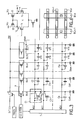
- FIG. 3 shows a memory according to the invention with a memory cell C1 comprising a floating gate transistor 1.
- the floating gate 2 of this transistor is interposed between a control gate 3 and a drain 4 and a source 5 connected together.
- the gate 3 is connected to a word line WL0, and the drain 4 and source 5 are connected together to a bit line BL0.
- the other cells C2 to Cn and Cm are represented schematically by their equivalent capacity Ca connected between one of the bit lines BL0 to BLm and one of the word lines WL0 to Wln.
- the cell C3 adopts a symbolism clearly showing that there is only one useful diffusion in the device of the invention.
- the bit and word lines are arranged matrix.
- decoders 6 and 7 are also related to decoders 6 and 7 for bit line decoding and word line decoding respectively. These decoders receive address signals making it possible to select each cell in turn, or possibly several at the same time. This solution is symbolized here by the control of transistors, connected in series with the bit lines and becoming conducting when they receive a signal decoded by the decoder. The selected bit line is then switched on with the read system.
- the memory also includes a precharge circuit supplied by a precharge voltage greater than
- the PRECH signal is applied to the control gate of a transistor 8 interposed between a connection Vbl connected to a bit line input of the decoder and to the precharge supply.
- the voltage must be greater than
- the memory also includes, in one example, two additional bit lines BLT0 and BLT1. These two bit lines are linked together and to a Vdum connection. One of the bit lines, BLT0 only serves programmed cells, the other BLT1 only erased cells.
- a read circuit 9 includes a differential amplifier receiving the signals supplied over the Vbl and Vdum connections.
- This differential amplifier of known type has two branches 10 and 11 between the general supply Vcc of the circuit and the electrical ground. Each branch comprises a P-type transistor, respectively 12 and 13, in series with an N-type transistor, respectively 14 and 15.
- the control gates of the transistors 12 and 13 are connected together and between the transistor 12 and the transistor 14.
- the transistor 14 has its control gate connected to the connection Vbl.
- the transistor 15 has its control gate connected to the Vdum connection.
- the output 5 for reading from the memory is the midpoint between the transistors 13 and 15.
- the two branches 10 and 11 are connected together to ground by a connection transistor establishing this connection at the appropriate times to avoid causing the circuit 9 to be charged reading unnecessarily outside of these times.
- FIGS. 4a to 4g show timing diagrams respectively of the precharge signals, bit line selection or addressing, word line selection or addressing, and of signals available on the cell bit line selected, on the bit lines of unselected cells, on the word line of the selected cell, and on those of unselected cells.
- bit lines For reading, for the duration of a precharge order, for example all the bit lines are preloaded. They are preloaded at least to
- Cbl parsitic capacity of the bit line connection itself
- the reference voltage is an average voltage, delivered by the bit lines BLT0 and BLT1 connected together, between the voltage delivered by an erased cell and a programmed cell read together.
- ⁇ V1 - 109 mV.
- the differential amplifier 9 is capable of detecting these differences.
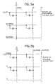
- Figures 5a and 5b show the voltages to be applied to the bit and word lines contributing to a selected cell to be programmed or erased. (pointed by arrows), as well as those that must be applied during these operations on the other lines contributing to the unselected cells.
- the programming voltage VPROG is applied by the bit line on the drain, and 0 Volts by the word line on the grid of the selected cell.
- half of the programming voltage is applied to all unselected word lines and 0 volts to the bit lines where the cell must not change state. For erasure, the direction of the electric field is reversed.
- a great advantage of this structure is that you can erase or program only one cell at a time. But you can also program or delete entire lines. For example, to erase all the cells of a line, it is brought to VPROG while keeping all the bit lines at 0. For the lines or columns not selected, the voltage 1/2 VPROG is used. It makes it possible to have on the unselected cells an electric field half as strong, insufficient to trigger a tunnel effect necessary for programming or erasing.
- FIG. 6 shows the word lines WLn, WLn-1 produced in the form of a second level polysilicon strip and capable of playing in themselves the role of control grid when they are placed above (with isolation) engraved plates, marked with hatching, made of first level polysilicon and playing the role of floating grids.
- a "drain" region has been diffused in the substrate, parallel to these word lines, and slightly below in the case where there is overlap.
- electrical connections are made between its drain diffusions and the metallized bit lines BLm, BLm-1 surmounting the word lines and being perpendicular to the latter. Drain broadcasts and connections with bit lines can take place between each word line, cell C1, or every other time, cell C3.
Abstract
Description
La présente invention a pour objet une mémoire EEPROM (Electrically Erasable and Programmable Read Only Memory) munie d'une cellule mémoire à mémorisation capacitive. Elle concerne aussi le procédé de lecture d'une telle cellule mémoire. Elle trouve son application dans le domaine des mémoires non volatiles. Celui-ci correspond aux cellules mémoires munies chacune d'un transistor à grille flottante comme organe de mémorisation. Le but de l'invention est d'augmenter la densité d'intégration de ces cellules sur un même substrat semiconducteur. Les cellules de l'invention permettent de stocker d'une façon durable un état logique binaire (1 ou 0), ou autre, même si on coupe l'alimentation du circuit électronique auquel elles sont connectées. Les avantages des cellules de l'invention sont les suivants:
- très faible taille géométrique de la cellule, d'où possibilité des réaliser des mémoires très denses;
- consommation de courant nulle en lecture et en programmation, ce qui est très intéressant pour des cartes à puces sans contact ou dans le domaine spatial;
- utilisation de technologies de fabrication standard existantes, celles des cellules dites EEPROM ou des cellules dites FLASH-EEPROM;
- possibilité d'écrire un 0 ou un 1 dans une seule cellule à la fois au lieu de devoir traiter tout un bloc;
- plus grande rapidité de lecture grâce à une lecture à courant nul.
- very small geometric size of the cell, hence the possibility of producing very dense memories;
- zero current consumption in reading and programming, which is very advantageous for contactless smart cards or in the space sector;
- use of existing standard manufacturing technologies, those of cells called EEPROM or cells called FLASH-EEPROM;
- possibility to write a 0 or a 1 in one cell at a time instead of having to process an entire block;
- faster reading speed thanks to zero current reading.
On connaît les cellules mémoires non volatiles comportant un transistor à grille flottante. On stocke des charges électriques sur cette grille flottante. Le transistor conduit ou se bloque suivant l'état mémorisé, suivant le type ou le nombre des charges stockées. Ces cellules sont de trois types. On distingue les cellules EPROM, les cellules EEPROM et les cellules FLASH-EEPROM. Avec une cellule EPROM, la grille flottante peut être chargée d'électrons ou déchargée. Le transistor à grille flottante conduit quand la grille flottante est dechargée. La densité d'intégration de ces cellules est bonne mais le courant de programmation (pour injecter les électrons dans la grille flottante) est important. La tension de programmation doit donc être fournie depuis l'extérieur du circuit intégré qui comporte la mémoire. Ces cellules ne sont pas effaçable électriquement: elles doivent être effacées par un rayonnement ultraviolet, ce qui provoque en outre l'effacement de toute la mémoire et non pas d'une seule cellule à la fois. Pour la lecture d'une telle cellule, comme pour la lecture des cellules des deux autres types, on mesure l'intensité d'un courant dit de lecture passant au travers de ce transistor.We know about non-volatile memory cells comprising a floating gate transistor. Electric charges are stored on this floating grid. The transistor conducts or blocks according to the memorized state, according to the type or the number of stored charges. These cells are of three types. A distinction is made between EPROM cells, EEPROM cells and FLASH-EEPROM cells. With an EPROM cell, the floating grid can be charged with electrons or discharged. The floating gate transistor conducts when the floating gate is discharged. The integration density of these cells is good, but the programming current (to inject the electrons into the floating grid) is important. The programming voltage must therefore be supplied from outside the integrated circuit which contains the memory. These cells cannot be erased electrically: they must be erased by ultraviolet radiation, which also causes the erasure of all memory and not of a single cell at a time. For the reading of such a cell, as for the reading of cells of the two other types, the intensity of a so-called reading current passing through this transistor is measured.
Avec une mémoire EEPROM, l'accès à une cellule doit être établi au travers d'un transistor d'accès: la densité d'intégration en est réduite par quatre. L'oxyde de grille interpose entre la grille flottante et le canal de conduction du transistor est bien plus faible que pour une cellule EPROM, il est de l'ordre de 7nm. Le transistor à grille flottante conduit lorsque la grille flottante est chargée de trous, il se bloque lorsqu'elle est chargée d'électrons. Les cellules sont programmables et effaçables par bloc.With an EEPROM memory, access to a cell must be established through an access transistor: the integration density is reduced by four. The gate oxide interposed between the floating gate and the conduction channel of the transistor is much weaker than for an EPROM cell, it is of the order of 7 nm. The floating gate transistor conducts when the floating gate is charged with holes, it blocks when it is charged with electrons. The cells are programmable and erasable by block.
Les cellules FLASH-EEPROM ont une allure technologique du même type que les EEPROM, mais sans transistor d'accès. Leur densité d'intégration est plus grande. Cependant, le procédé de fabrication est difficile à mettre au point, au moment de la programmation le temps de programmation est très long (quelques secondes), et les tensions de seuil de programmation doivent être très précisément contrôlées. La cellule consomme du courant en effacement et en lecture.FLASH-EEPROM cells have the same technological appearance as EEPROMs, but without access transistor. Their integration density is greater. However, the manufacturing process is difficult to develop, at the time of programming the programming time is very long (a few seconds), and the programming threshold voltages must be very precisely controlled. The cell consumes current in erasure and in reading.
Les grilles de toutes ces cellules sont de préférence l'une au dessus de l'autre, mais il est tout à fait envisageable de réaliser une grille de commande enterrée, surmontée de la grille flottante. Cette dernière vient ensuite surplomber le bord d'une région de drain d'un transistor, ou tout simplement une région dopée. Il en sera de même pour les cellules de l'invention bien que, pour simplifier, la présente description concerne plus précisément les structures à empilage.The grids of all these cells are preferably one above the other, but it is entirely conceivable to produce a buried control grid, surmounted by the floating grid. The latter then overhangs the edge of a drain region of a transistor, or quite simply a doped region. It will be the same for the cells of the invention although, for simplicity, the present description relates more precisely to stacking structures.
Une cellule, dans l'état de la technique ou dans l'invention, est dite programmée si elle a reçue des trous sur sa grille flottante. Elle est dite effacée si elle a reçu des électrons. Quand elle est programmée son seuil de conduction est negatif: par exemple la valeur de ce seuil est - 2 V. Ainsi cette cellule se mettrait à conduire si la tension appliquée sur sa grille de commande de son transistor etait supérieure à - 2 V, alors qu'elle est polarisée par 5 V sur son drain et 0 V sur sa source. Quand elle est effacée son seuil de conduction est positif: par exemple 4 V, dans les mêmes conditions que ci-dessus. Le seuil de conduction est donc plus grand dans l'état effacé que dans l'état programmé.A cell, in the state of the art or in the invention, is said to be programmed if it has received holes on its floating grid. It is said to be erased if it has received electrons. When it is programmed its conduction threshold is negative: for example the value of this threshold is - 2 V. Thus this cell would start to conduct if the voltage applied to its control gate of its transistor was greater than - 2 V, then that it is polarized by 5 V on its drain and 0 V on its source. When it is deleted, its conduction threshold is positive: for example 4 V, under the same conditions as above. The conduction threshold is therefore greater in the erased state than in the programmed state.
L'invention a pour objet de remédier aux inconvénients cites en mettant en oeuvre un principe physique différent de celui de la conduction des transistors à grille flottante. Dans l'invention on surveille la variation de la capacité d'un transistor ou plutôt d'un dispositif de type MOS à grille flottante en fonction de la tension appliquée sur sa grille de commande. On constate en effet qu'il existe une capacité entre la grille flottante et le drain du transistor, de même qu'il existe une capacité entre cette grille flottante et le substrat semiconducteur, à l'endroit du canal de conduction. Cette dernière capacité varie d'une part fortement selon que le transistor est passant ou non. Soit cette capacité existe entre la grille flottante et le substrat si la tension de la grille de commande est inférieure au seuil de conduction du transistor (et alors elle est faible); soit elle existe entre la grille flottante et le canal de conduction crée par le transistor si la tension de la grille flottante dépasse la tension de seuil de conduction du transistor (et alors elle est forte). D'autre part, quand le transistor conduit cette capacité grille flottante-canal de conduction s'additionne à la capacité grille flottante-drain puisqu'elle lui est connectée en parallèle par le canal de conduction.The object of the invention is to remedy the drawbacks cited by implementing a principle physics different from that of the conduction of floating gate transistors. In the invention, the variation in the capacitance of a transistor or rather of a floating gate MOS type device is monitored as a function of the voltage applied to its control gate. It can be seen that there is a capacitance between the floating gate and the drain of the transistor, just as there is a capacitance between this floating gate and the semiconductor substrate, at the location of the conduction channel. This latter capacity varies on the one hand strongly depending on whether the transistor is on or not. Either this capacity exists between the floating gate and the substrate if the voltage of the control gate is lower than the conduction threshold of the transistor (and then it is low); either it exists between the floating gate and the conduction channel created by the transistor if the voltage of the floating gate exceeds the conduction threshold voltage of the transistor (and then it is high). On the other hand, when the transistor conducts this floating gate-conduction channel capacitance is added to the floating gate-drain capacitance since it is connected to it in parallel by the conduction channel.
Dans l'invention, la cellule proposée a son drain et sa source court-circuités, ou bien même l'un d'entre eux n'existe même pas. Il n'y a donc plus a proprement parlé de transistor. L'existence ou non d'un canal de conduction s'explique cependant de la manière suivante. Il existe quand la tension sur la grille de commande est supérieure à la tension de seuil. Quand ce canal existe la capacité grille flottante-canal existe. Par contre entre les grilles flottantes (en polysilicium de premier niveau) et les grilles de commande (en polysilicium de deuxième niveau dans les structures à empilage) ou entre elles et la zone de conduction du transistor, ou le substrat semiconducteur, il n'y a aucun courant.In the invention, the proposed cell has its drain and its source short-circuited, or even one of them does not even exist. There is therefore no longer, strictly speaking, a transistor. The existence or not of a conduction channel can however be explained as follows. It exists when the voltage on the control gate is greater than the threshold voltage. When this channel exists, the floating gate-channel capacity exists. On the other hand between the floating grids (in first level polysilicon) and the control grids (in second level polysilicon in stacking structures) or between them and the conduction area of the transistor, or the semiconductor substrate, there is no current.
Si le canal n'existe pas, la capacité entre la grille flottante et le substrat subsiste. Celle-ci est cependant faible pour une tension de la grille de commande avoisinante ou inférieure à la tension de seuil. La capacité qui est utilisée dans le dispositif de l'invention est la capacité entre la grille flottante et une ligne de bit constituée schématiquement par un drain. Quand la tension de la grille de commande dépasse la tension du seuil, le canal est créé. Il existe alors une connexion électrique entre le canal et une diffusion de drain, ou de source, servant de ligne de bit. Si cette tension est inférieure à cette valeur, même si le canal existe, il n'y a en fait pas de connexion électrique entre le canal et la diffusion drain ou source. Ceci est dû à la présence de la zone désertée créée autour de la diffusion (n⁺) de ce drain ou de cette source. Ce comportement est utilisé pendant la lecture.If the channel does not exist, the capacity between the floating gate and the substrate remains. However, this is low for a voltage of the control gate close to or lower than the threshold voltage. The capacity which is used in the device of the invention is the capacity between the floating gate and a bit line schematically constituted by a drain. When the control gate voltage exceeds the threshold voltage, the channel is created. There is then an electrical connection between the channel and a drain or source diffusion serving as a bit line. If this voltage is lower than this value, even if the channel exists, there is in fact no electrical connection between the channel and the drain or source diffusion. This is due to the presence of the deserted area created around the diffusion (n⁺) of this drain or this source. This behavior is used during reading.
L'invention a donc pour objet une cellule mémoire d'un circuit intégré dans un substrat semiconducteur, comportant une grille de commande commandant et étant isolée d'une grille flottante, cette grille flottante étant isolée du substrat semiconducteur, cet isolement comportant au moins une fenêtre en un oxyde tunnel, caractérisée en ce que cette grille surmonte en partie à l'endroit de cette fenêtre en oxyde tunnel une région unique de ce substrat dopée avec des impuretés d'un type opposé aux impuretés qui dope le substrat alentour de cette région unique. La fenêtre tunnel peut par ailleurs occuper toute la surface de l'isolement entre la grille flottante et le substrat. Dans la cellule de l'invention il n'y a que deux accès : un sur la grille de commande et un sur la région. Il n'y a pas alors de région pouvant constituer une source, et qui serait reliée par ailleurs à la masse ou à un autre potentiel.The subject of the invention is therefore a memory cell of an integrated circuit in a semiconductor substrate, comprising a command grid controlling and being isolated from a floating grid, this floating grid being isolated from the semiconductor substrate, this isolation comprising at least one window in a tunnel oxide, characterized in that this grid partially overcomes at the location of this window in tunnel oxide a single region of this substrate doped with impurities of a type opposite to the impurities which boosts the substrate surrounding this region unique. The tunnel window can also occupy the entire surface of the insulation between the floating grid and the substrate. In the cell of the invention there are only two accesses: one on the control grid and one on the region. There is then no region which could constitute a source, and which would otherwise be connected to the ground or to another potential.
Elle a également pour objet une cellule mémoire d'un circuit intégré dans un substrat semiconducteur, comportant une grille de commande commandant et étant isolée d'une grille flottante, cette grille flottante étant isolée du substrat semiconducteur, cet isolement comportant au moins une fenêtre en un oxyde tunnel au dessus d'un canal de conduction d'un transistor réalisé dans le substrat semiconducteur, caractérisée en ce que les régions drain et source de ce transistor sont reliées électriquement. Dans ce sens on comprendra comme formant un transistor au sens de l'invention tout couple de régions diffusées dans le substrat, court-circuitées ensemble, et surmonte d'une grille flottante.It also relates to a memory cell of an integrated circuit in a semiconductor substrate, comprising a command grid controlling and being isolated from a floating grid, this floating grid being isolated from the semiconductor substrate, this isolation comprising at least one window in a tunnel oxide above a conduction channel of a transistor produced in the semiconductor substrate, characterized in that the drain and source regions of this transistor are electrically connected. In this sense, it will be understood as forming a transistor within the meaning of the invention any pair of regions diffused in the substrate, short-circuited together, and surmounted by a floating gate.
Elle a enfin pour objet un procédé de lecture d'une cellule mémoire dans une mémoire munie de cellules avec dispositif à grille flottante, ce dispositif comportant une grille de commande reliée à une ligne de mot et une région source, ou une région drain, reliée à une ligne de bit, cette cellule étant dans un état programmée ou effacée, le seuil de conduction d'un canal de conduction du dispositif à grille flottante étant plus faible dans l'état programmé que dans l'état effacé, caracterisé en ce que
- on précharge les lignes de bit à une tension dont la valeur est au moins egale à la valeur absolue du seuil de conduction de la cellule pour un état programmé pour minimiser les capacités des lignes de bit,
- on sélectionne la ligne de bit et la ligne de mot concernées par la cellule à lire, et
- on compare à une tension de référence la tension restant sur la ligne de bit sélectionnée et on en déduit l'état lu.
- the bit lines are preloaded at a voltage whose value is at least equal to the absolute value of the cell conduction threshold for a state programmed to minimize the capacities of the bit lines,
- the bit line and the word line concerned by the cell to be read are selected, and
- the voltage remaining on the selected bit line is compared to a reference voltage and we deduce therefrom read status.
L'invention sera mieux comprise à la lecture de la description qui suit et à l'examen des figures qui l'accompagnent. Celles-ci ne sont données qu'à titre indicatif et nullement limitatif d l'invention. Les figures montrent:
- figures 1a à 1c: une représentation schématique de l'architecture des capacités dans un transistor ou plus généralement dans un dispositif à grille flottante;
- figures 2a et 2b: des diagrammes montrant l'évolution de la capacité grille flottante-drain du dispositif à grille flottante, en fonction de la tension appliquée sur la grille de commande, dans le cas d'une cellule effacée ou programmée respectivement;
- figure 3: une mémoire selon l'invention et les particularités de son système de lecture;
- figures 4a à 4g: des diagrammes temporels montrant pour trois utilisations de la mémoire les tension appliquées dans son circuit de commande;
- figures 5a et 5b: une représentation simplifiée des tensions applicables sur des lignes de bit et ligne de mot de la mémoire pour programmer ou effacer respectivement une cellule mémoire ;
- figure 6 : un schéma d'implantation de cellules mémoires de la mémoire dans un substrat semiconducteur.
- FIGS. 1a to 1c: a schematic representation of the architecture of the capacitors in a transistor or more generally in a floating gate device;
- FIGS. 2a and 2b: diagrams showing the evolution of the floating gate-drain capacity of the floating gate device, as a function of the voltage applied to the control gate, in the case of a cell erased or programmed respectively;
- Figure 3: a memory according to the invention and the features of its reading system;
- FIGS. 4a to 4g: time diagrams showing for three uses of the memory the voltages applied in its control circuit;
- FIGS. 5a and 5b: a simplified representation of the voltages applicable on bit lines and word lines of the memory for programming or erasing respectively a memory cell;
- FIG. 6: a diagram of implantation of memory cells of the memory in a semiconductor substrate.
Les figures la 1a 1c montrent des cellules selon l'invention de divers types : respectivement théorique, dérivée d'une cellule EEPROM, ou dérivée d'une cellule FLASH-EEPROM. Sur ces figures un substrat semiconducteur T contient une cellule selon l'invention. Celle-ci est munie d'une grille de commande GC, réalisée en une couche de polysilicium de deuxième niveau. La grille GC est séparée par une couche d'oxyde d'une grille flottante GF, réalisée en une couche de polysilicium de premier niveau. La grille GF est séparée du substrat T, au moins en un endroit, par une couche d'oxyde tunnel OT de faible épaisseur. Dans le cas de la cellule dérivée d'une cellule EEPROM, sous l'oxyde OT on trouve dans le substrat une implantation tunnel IT favorisant l'injection des charges électroniques dans la grille GF. Dans le cas de la cellule dérivée de la cellule FLASH-EEPROM, tout l'oxyde sous la grille GF est un oxyde tunnel de faible épaisseur e.Figures 1a 1c show cells according to the invention of various types: respectively theoretical, derived from an EEPROM cell, or derived from a FLASH-EEPROM cell. In these figures a semiconductor substrate T contains a cell according to the invention. This is provided with a GC control grid, made of a second level polysilicon layer. The grid GC is separated by a layer of oxide from a floating grid GF, produced in a layer of polysilicon of first level. The grid GF is separated from the substrate T, at least in one place, by a layer of tunnel oxide OT of small thickness. In the case of the cell derived from an EEPROM cell, under the OT oxide there is in the substrate an IT tunnel implantation promoting the injection of electronic charges into the GF grid. In the case of the cell derived from the FLASH-EEPROM cell, all the oxide under the GF grid is a tunnel oxide of thin thickness e.
Dans le cas de la figure la, la grille GF est superposée sur le canal de conduction d'un transistor comportant une source S et un drain D reliés entre eux par une connexion CO. Dans le cas des figures 1b et 1c les sources ne sont pas realisées. Si elles le sont elles sont également connectées aux drains D. Les drains ou sources sont realisés sous forme de diffusion n⁺ dans le substrat T de type p. En pratique la meilleure cellule, celle qui prend le moins de place est celle dans laquelle les régions sources ne sont pas réalisées parce qu'en fait elles sont inutiles.In the case of FIG. 1a, the gate GF is superimposed on the conduction channel of a transistor comprising a source S and a drain D connected together by a connection CO. In the case of FIGS. 1b and 1c the sources are not produced. If they are, they are also connected to the drains D. The drains or sources are produced in the form of n⁺ diffusion in the p-type substrate T. In practice, the best cell, the one that takes up the least space, is the one in which the source regions are not produced because in fact they are useless.
Les capacités existant entre ces différents éléments du dispositif à grille flottante sont les suivantes:
- Cp1p2 capacité entre la grille GC et la grille GF.
- Cgd capacité entre la grille GF et le drain D (ou plutôt la diffusion assimilée à ce drain).
- Cgs capacité entre la grille GF et la source S du transistor. Dans la mesure où S est reliée à D par une connexion CO, ou dans la mesure où S n'existe même pas, on assimilera Cgs à Cgd.
- Ccan capacité existant entre la grille GF et le substrat T quand la tension sur la grille GC est supérieure à la tension de seuil de conduction du transistor.
- Cgt capacité entre grille GF et substrat T quand le transistor ne conduit pas. Elle est négligeable.
- Cp1p2 capacity between the grid GC and the grid GF.
- Cgd capacity between the grid GF and the drain D (or rather the diffusion assimilated to this drain).
- Cgs capacitance between the gate GF and the source S of the transistor. Insofar as S is connected to D by a connection CO, or insofar as S does not even exist, we will assimilate Cgs to Cgd.
- Ccan capacity existing between the grid GF and the substrate T when the voltage on the grid GC is greater than the conduction threshold voltage of the transistor.
- Cgt capacitance between gate GF and substrate T when the transistor does not conduct. It is negligible.
La capacité Cgd elle-même se décompose en capacité de recouvrement Crec entre la partie du drain qui va sous la grille GF et la grille GF elle-même, et en capacité d'implantation tunnel Cit. Cette dernière n'est ici visible que dans la variante derivée de la technologie EEPROM où une implantation tunnel est effectuée sous la partie d'oxyde tunnel.The Cgd capacity itself breaks down into Crec covering capacity between the part of the drain which goes under the GF grid and the GF grid itself, and into Cit tunnel installation capacity. The latter is only visible here in the variant derived from the EEPROM technology where a tunnel implantation is carried out under the tunnel oxide part.
Ces capacités sont mises en circuit de la manière suivante. La capacité Cp1p2 est en série avec les capacités Cgd et Ccan. Lorsque le canal est connecté ces deux dernières capacités s'additionnent et jouent ensemble le rôle de la capacité Cgd. Quand il nest pas connecte, seule la capacité intrinsèque Cgd intervient dans le schéma équivalent de connexion. Cette dernière, quand elle intervient seule, est équivalente à Crec. L'évolution de la capacité grille flottante-drain en fonction de la tension appliquée sur la grille de commande GC est représentée sur les figures 2a et 2b. Respectivement, dans l'état efface (un 1 est écrit dans la cellule) la tension de seuil de création de la connexion du canal est VT1. Dans un exemple VT1 vaut 4 Volts. Dans l'état programmé (un 0 est écrit dans la cellule) le seuil de création de la connexion du canal est VT0. Dans un exemple VT0 vaut - 2 Volts. Dès que la tension sur la grille GC devient supérieure à la tension de seuil la capacité Cgd passe de la valeur Crec à la valeur Crec + Ccan + Cit (éventuellement pour cette dernière).These capacities are connected in the following manner. The Cp1p2 capacity is in series with the Cgd and Ccan capacities. When the channel is connected, these last two capacities add up and together play the role of the Cgd capacity. When it is not connected, only the intrinsic capacity Cgd intervenes in the equivalent connection scheme. The latter, when it intervenes alone, is equivalent to Crec. The evolution of the floating gate-drain capacity as a function of the voltage applied to the control gate GC is shown in FIGS. 2a and 2b. Respectively, in the erased state (a 1 is written in the cell) the threshold voltage for creating the connection of the channel is VT1. In an example VT1 is worth 4 Volts. In the programmed state (a 0 is written in the cell) the threshold for creating the channel connection is VT0. In an example VT0 is worth - 2 Volts. As soon as the voltage on the grid GC becomes greater than the threshold voltage, the capacity Cgd goes from the value Crec to the value Crec + Ccan + Cit (possibly for the latter).
Le fonctionnement de la cellule est le suivant. Grâce à l'existence d'une fenêtre tunnel (de 10nm environ d'épaisseur) des charges peuvent être conduites sur la grille GF si on applique un champ électrique suffisamment grand (de l'ordre de 10 Mv/cm) à travers l'oxyde tunnel. Ce champ est obtenu en portant la grille GC à environ 20 V quand le drain est 0 V, ou vice versa. Suivant la direction du champ appliqué, on stocke soit des électrons soit des trous. L'apport de ces charges sur la grille flottante permet de modifier la tension de seuil du transistor MOS, vue de la grille GC. Cette programmation est similaire dans son principe à celle des cellules EEPROM ou FLASH-EEPROM de l'état de la technique.The operation of the cell is as follows. Thanks to the existence of a tunnel window (about 10nm thick) loads can be conducted on the GF grid if a sufficiently large electric field (of the order of 10 Mv / cm) is applied through the tunnel oxide. This field is obtained by bringing the grid GC to approximately 20 V when the drain is 0 V, or vice versa. Depending on the direction of the applied field, either electrons or holes are stored. The contribution of these charges to the floating gate makes it possible to modify the threshold voltage of the MOS transistor, seen from the gate GC. This programming is similar in principle to that of the state-of-the-art EEPROM or FLASH-EEPROM cells.
Pour une cellule effacée la capacité de la cellule vue de la grille GC est :![]()
![]()
Pour une cellule programmée la capacité de la cellule vue de la grille GC est :![]()
L'inconvenient d'une cellule capacitive dérivée d'une cellule EEPROM vient de ce que la capacité Crec est relativement grande (il y a alors moins de différence entre Ca0 et Ca1), ce qui détériore la sensibilité en lecture. Pour diminuer cette capacité Crec, la fenêtre tunnel FT est repoussée vers le bord de la grille GF, dans le sens de la flèche 1 par exemple.For a programmed cell, the capacity of the cell seen from the GC grid is: ![]()
The drawback of a capacitive cell derived from an EEPROM cell comes from the fact that the Crec capacity is relatively large (there is then less difference between Ca0 and Ca1), which deteriorates the sensitivity in reading. To decrease this Crec capacity, the tunnel window FT is pushed back towards the edge of the grid GF, in the direction of
Dans la technologie dérivée de la technologie FLASH-EEPROM, où tout l'oxyde de grille GF est un oxyde tunnel, on peut pour améliorer la programmation ou l'effacement ajouter une implantation de type LDD sur le drain pour l'étendre légèrement sous la grille GF. Ceci comporte l'avantage de minimiser la capacité Crec et ainsi d'avoir une cellule la plus petite possible.In the technology derived from the FLASH-EEPROM technology, where all of the GF gate oxide is a tunnel oxide, it is possible to improve programming or erasure add an LDD type implantation on the drain to extend it slightly below the GF grid. This has the advantage of minimizing the Crec capacity and thus of having the smallest possible cell.
la figure 3 montre une mémoire selon l'invention avec une cellule mémoire C1 comportant un transistor à grille flottante 1. La grille flottante 2 de ce transistor est interposée entre une grille de commande 3 et un drain 4 et une source 5 reliés entre eux. La grille 3 est reliée à une ligne de mot WL0, et les drain 4 et source 5 sont relies ensemble à une ligne de bit BL0. Les autres cellules C2 à Cn et Cm sont représentées schématiquement par leur capacité équivalente Ca connectée entre une des lignes de bit BL0 à BLm et une des lignes de mot WL0 à Wln. La cellule C3 adopte un symbolisme montrant clairement qu'il n'y a qu'une diffusion utile dans le dispositif de l'invention. Les lignes de bit et de mot sont arrangées matriciellement. Elles sont également en relation avec des décodeurs respectivement 6 et 7 de décodage de ligne de bit et de décodage de ligne de mot. Ces décodeur reçoivent des signaux d'adresse permettant de sélectionner chaque cellule à son tour, ou éventuellement plusieurs en même temps. Cette solution est symbolisée ici par la commande de transistors, montes en série avec les lignes de bit et devenant passant quand il reçoivent un signal décodé par le décodeur. La ligne de bit sélectionnée est alors mise en circuit avec le système de lecture. La mémoire comporte aussi un circuit de précharge alimenté par une tension de précharge supérieure à |VT0| et commandé par un signal de précharge PRECH. Le signal PRECH est applique sur la grille de commande d'un transistor 8 interposé entre une connexion Vbl reliée à une entrée ligne de bit du décodeur et à l'alimentation de précharge. La tension doit être supérieure à |VTO| parce que, d'une cellule à l'autre, la tension de seuil peut varier et qu'il vaut mieux prendre des précautions.FIG. 3 shows a memory according to the invention with a memory cell C1 comprising a floating
La mémoire comporte encore, dans un exemple, deux lignes de bits supplémentaires BLT0 et BLT1. Ces deux lignes de bits sont reliées entre elles et à une connexion Vdum. Une des lignes de bit, BLT0 ne dessert que des cellules programmées, l'autre BLT1 que des cellules effacées.The memory also includes, in one example, two additional bit lines BLT0 and BLT1. These two bit lines are linked together and to a Vdum connection. One of the bit lines, BLT0 only serves programmed cells, the other BLT1 only erased cells.
Un circuit 9 de lecture comporte un amplificateur differentiel recevant les signaux dispensé sur les connexions Vbl et Vdum. Cet amplificateur différentiel de type connu comporte deux branches 10 et 11 entre l'alimentation générale Vcc du circuit et la masse électrique. Chaque branche comporte un transistor de type P, respectivement 12 et 13, en série avec un transistor de type N, respectivement de 14 et 15. Les grilles de commande des transistors 12 et 13 sont reliées entre elles et entre le transistor 12 et le transistor 14. Le transistor 14 a sa grille de commande reliée à la connexion Vbl. Le transistor 15 a sa grille de commande reliée à la connexion Vdum. La sortie 5 de lecture de la mémoire est le point milieu entre les transistors 13 et 15. Les deux branches 10 et 11 sont reliées ensemble à la masse par un transistor de liaison établissant cet liaison aux moments opportuns pour éviter de faire débiter le circuit 9 de lecture inutilement en dehors de ces moments.A
Les figures 4a à 4g montrent des diagrammes temporels respectivement des signaux de précharge, de sélection ou d'adressage de ligne de bit, de sélection ou d'adressage de ligne de mot, et de de signaux disponibles sur la ligne de bit de la cellule sélectionnée, sur les lignes de bit des cellules non sélectionnées, sur la ligne de mot de la cellule sélectionnée, et sur celles des cellules non sélectionnées.FIGS. 4a to 4g show timing diagrams respectively of the precharge signals, bit line selection or addressing, word line selection or addressing, and of signals available on the cell bit line selected, on the bit lines of unselected cells, on the word line of the selected cell, and on those of unselected cells.
Pour la lecture, pendant la durée d'un ordre de précharge, par exemple toutes les lignes de bit sont préchargées. Elles sont préchargées au minimum à |VT0| qui représente la tension de seuil d'une cellule programmée. Dans l'exemple où VT0 vaut - 2 Volts, on précharge donc les lignes de bit à plus que 2 Volts, par exemple à 2,5 Volts. Ceci permet de minimiser la capacité de chaque ligne de bit. En effet, la capacité Ccan d'une cellule programmée ne s'ajoute plus à la capacité Crec de cette cellule si la tension de drain de cette cellule est supérieure à |VT0|. Avec cette condition la capacité en précharge d'une ligne de bit est égale à Cbl (capacité parasite de la connexion de ligne de bit elle-même) plus n fois Crec s'il y a n cellules sur la même ligne de bit.For reading, for the duration of a precharge order, for example all the bit lines are preloaded. They are preloaded at least to | VT0 | which represents the threshold voltage of a programmed cell. In the example where VT0 is equal to - 2 Volts, the bit lines are therefore preloaded to more than 2 Volts, for example to 2.5 Volts. This minimizes the capacity of each bit line. Indeed, the capacity Ccan of a programmed cell no longer adds to the capacity Crec of this cell if the drain voltage of this cell is greater than | VT0 |. With this condition the precharging capacity of a bit line is equal to Cbl (parasitic capacity of the bit line connection itself) plus n times Crec if there are cells on the same bit line.
Pendant la lecture, après la précharge, seule la ligne de bit reliée à la cellule à sélectionner est reliée à l'amplificateur 9. De même pendant la lecture seule la ligne de mot correspondant à la cellule à sélectionner est portée à V Volts, par exemple 5 Volts, ou même plus si on utilise une technique de multiplication de tension. Les autres lignes de mot restent à 0 Volts. Par exemple WL0 est portée à 5 Volts. La sélection de la ligne de mot est ultérieure à la fin de la précharge.During reading, after preloading, only the bit line connected to the cell to be selected is connected to
Considérons que la cellule C1 est dans un état programme et qu'elle est lue. Au moment de la lecture elle fait passer sur la ligne de bit BL1 une variation de tension egale à
δV = V . Ca / (Ca + Cbltot) où V vaut dans l'exemple 5 Volts, où Ca est la capacité équivalente de la cellule et Cbltot la capacité de la totalité de la ligne de bit. On peut écrire encore que![]()
Le premier terme est dû à la capacité Cgd avant que la ligne de mot ne dépasse la tension de création du canal. Le deuxième terme représente la tension passée sur la ligne de bit après que la connexion de canal soit créée.Let us consider that cell C1 is in a program state and that it is read. At the time of reading, it passes on the bit line BL1 a voltage variation equal to
δV = V. Ca / (Ca + Cbltot) where V is in the example 5 Volts, where Ca is the equivalent capacity of the cell and Cbltot the capacity of the entire bit line. We can still write that ![]()
The first term is due to the capacity Cgd before the word line exceeds the creation voltage of the channel. The second term represents the voltage passed over the bit line after the channel connection is created.
Si la cellule C1 est dans un état effacé au moment de la lecture, la tension qui passe sur la ligne de bit est seulement
δV = V . Cgd / (Cgd + Cbltot) puisque comme V (égal à 5 Volts) est inférieur à |VT1| + Vbl (égal à 4 Volts + 2,5 Volts) la capacité Ccan n'est pas utilisée dans le couplage : il n'y a pas de canal connecté à la diffusion n⁺.If cell C1 is in an erased state at the time of reading, the voltage passing over the bit line is only
δV = V. Cgd / (Cgd + Cbltot) since since V (equal to 5 Volts) is less than | VT1 | + Vbl (equal to 4 Volts + 2.5 Volts) the Ccan capacity is not used in the coupling: there is no channel connected to broadcast n⁺.
Pour effectuer la détection de l'état de la cellule lue on compare la tension finale sur la ligne de bit avec une tension de référence. La tension de référence est une tension moyenne, délivrée par les lignes de bit BLT0 et BLT1 reliées entre elles, entre la tension délivrée par une cellule effacée et une cellule programmée lues ensemble.To detect the state of the cell read, the final voltage on the bit line is compared with a reference voltage. The reference voltage is an average voltage, delivered by the bit lines BLT0 and BLT1 connected together, between the voltage delivered by an erased cell and a programmed cell read together.
Pour la détection d'un état programme (un 0), on obtient, dans le cas idéal où Crec est très inférieur à Ccan et où Ccan est de l'ordre du vingtième de Cbltot:![]()
![]()
Pour la détection d'un état effacé (un 1), on obtient, dans le cas idéal où Crec est très inférieur à Ccan et où Ccan est de l'ordre du vingtième de Cbltot:![]()
![]()
On s'aperçoit que les valeurs de δV sont environ symétriques par rapport à la tension moyenne de comparaison. Par exemple avec les valeurs données jusqu'ici elles valent δV0 = 104 mV et δV1 = - 109 mV. L'amplificateur differentiel 9 est capable de détecter ces différences.We can see that the values of δV are approximately symmetrical with respect to the average comparison voltage. For example with the values given so far they are worth δV0 = 104 mV and δV1 = - 109 mV. The
Les figures 5a et 5b montrent les tensions à appliquer sur les lignes de bit et de mot concourant à une cellule sélectionnée à programmer ou à effacer (pointées par des flèches), ainsi que celles qu'il faut appliquer pendant ces ces opérations sur les autres lignes concourant aux cellules non sélectionnées. Pendant la programmation, on applique la tension de programmation VPROG par la ligne de bit sur le drain, et 0 Volts par la ligne de mot sur la grille de la cellule sélectionnée. Pour ne pas affecter l'état des autres cellules, on applique la moitie de la tension de programmation sur toutes les lignes de mot non sélectionnées et 0 Volts sur les lignes de bits où la cellule ne doit pas changer d'état. Pour l'effacement on inverse le sens du champ électrique. Pour cela on applique VPROG sur la grille par l'intermédiaire de la ligne de mot, et 0 Volts sur le drain par l'intermédiaire de la ligne de bit de la cellule sélectionnée. Pour ne pas affecter le contenu des autres cellules, on porte les lignes de bit dont les cellules ne doivent pas changer d'état à 1/2 VPROG et toutes les autres lignes de mots à 0 Volts.Figures 5a and 5b show the voltages to be applied to the bit and word lines contributing to a selected cell to be programmed or erased. (pointed by arrows), as well as those that must be applied during these operations on the other lines contributing to the unselected cells. During programming, the programming voltage VPROG is applied by the bit line on the drain, and 0 Volts by the word line on the grid of the selected cell. In order not to affect the state of the other cells, half of the programming voltage is applied to all unselected word lines and 0 volts to the bit lines where the cell must not change state. For erasure, the direction of the electric field is reversed. To do this, apply VPROG to the grid via the word line, and 0 Volts to the drain via the bit line of the selected cell. In order not to affect the content of the other cells, the bit lines whose cells must not change state are brought to 1/2 VPROG and all the other word lines to 0 Volts.
Un grand avantage de cette structure est qu'on puisse effacer ou programmer une seule cellule à la fois. Mais on peut aussi programmer ou effacer des lignes entières. Par exemple pour effacer toutes les cellules d'une ligne on la porte à VPROG en maintenant toutes les lignes de bit à 0. Pour les lignes ou colonnes non sélectionnées la tension 1/2 VPROG est utilisée. Elle permet d'avoir sur les cellules non sélectionnées un champ électrique deux fois moins fort, insuffisant pour déclencher un effet tunnel nécessaire à la programmation ou l'effacement.A great advantage of this structure is that you can erase or program only one cell at a time. But you can also program or delete entire lines. For example, to erase all the cells of a line, it is brought to VPROG while keeping all the bit lines at 0. For the lines or columns not selected, the
La figure 6 montre les lignes de mot WLn, WLn-1 réalisées sous forme de bande de polysilicium de deuxième niveau et susceptible de jouer en elles même le rôle de grille de commande lorsqu'elles sont placées au-dessus (avec un isolement) de plaques gravées, marquées avec des hachures, réalisées en polysilicium de premier niveau et jouant le rôle de grilles flottantes. Entre la ligne WLn et la ligne WLn-1, on a diffusé dans le substrat une région de "drain", parallèlement à ces lignes de mot, et légèrement en dessous dans le cas où il y a recouvrement. Entre ces deux lignes de mots, au droit de l'alignement des plaques on réalise des connexions électriques entre ses diffusions de drain et les lignes de bit metallisées BLm, BLm-1 surmontant les lignes de mot et étant perpendiculaires à ces dernières. Les diffusions de drain et les connexions avec les lignes de bit peuvent prendre place entre chaque ligne de mot, cellule C1, ou une fois sur deux, cellule C3.FIG. 6 shows the word lines WLn, WLn-1 produced in the form of a second level polysilicon strip and capable of playing in themselves the role of control grid when they are placed above (with isolation) engraved plates, marked with hatching, made of first level polysilicon and playing the role of floating grids. Between the line WLn and the line WLn-1, a "drain" region has been diffused in the substrate, parallel to these word lines, and slightly below in the case where there is overlap. Between these two word lines, in line with the alignment of the plates, electrical connections are made between its drain diffusions and the metallized bit lines BLm, BLm-1 surmounting the word lines and being perpendicular to the latter. Drain broadcasts and connections with bit lines can take place between each word line, cell C1, or every other time, cell C3.
Claims (8)
Applications Claiming Priority (2)
| Application Number | Priority Date | Filing Date | Title |
|---|---|---|---|
| FR9106466 | 1991-05-29 | ||
| FR919106466A FR2690008B1 (en) | 1991-05-29 | 1991-05-29 | MEMORY WITH CAPACITIVE EFFECT EEPROM MEMORY CELL AND METHOD FOR READING SUCH A MEMORY CELL. |
Publications (2)
| Publication Number | Publication Date |
|---|---|
| EP0516516A1 true EP0516516A1 (en) | 1992-12-02 |
| EP0516516B1 EP0516516B1 (en) | 1998-11-11 |
Family
ID=9413241
Family Applications (1)
| Application Number | Title | Priority Date | Filing Date |
|---|---|---|---|
| EP92401408A Expired - Lifetime EP0516516B1 (en) | 1991-05-29 | 1992-05-22 | Memory with capacitive EEPROM cell and process for reading such a memory cell |
Country Status (6)
| Country | Link |
|---|---|
| US (2) | US5552621A (en) |
| EP (1) | EP0516516B1 (en) |
| JP (1) | JPH05206478A (en) |
| DE (1) | DE69227542T2 (en) |
| ES (1) | ES2127210T3 (en) |
| FR (1) | FR2690008B1 (en) |
Cited By (2)
| Publication number | Priority date | Publication date | Assignee | Title |
|---|---|---|---|---|
| WO2001073854A2 (en) * | 2000-03-25 | 2001-10-04 | Peregrine Semiconductor Corporation | Variable capacitor with programmability |
| US6690056B1 (en) | 1999-04-06 | 2004-02-10 | Peregrine Semiconductor Corporation | EEPROM cell on SOI |
Families Citing this family (12)
| Publication number | Priority date | Publication date | Assignee | Title |
|---|---|---|---|---|
| EP0737366B1 (en) * | 1994-10-28 | 2002-04-10 | Koninklijke Philips Electronics N.V. | Field effect device |
| FR2739706B1 (en) * | 1995-10-09 | 1997-11-21 | Inside Technologies | MEMORY CARD IMPROVEMENTS |
| FR2739737B1 (en) * | 1995-10-09 | 1997-11-21 | Inside Technologies | MEMORY CARD IMPROVEMENTS |
| US5925904A (en) * | 1996-04-03 | 1999-07-20 | Altera Corporation | Two-terminal electrically-reprogrammable programmable logic element |
| US5777361A (en) * | 1996-06-03 | 1998-07-07 | Motorola, Inc. | Single gate nonvolatile memory cell and method for accessing the same |
| IT1289540B1 (en) * | 1996-07-10 | 1998-10-15 | Sgs Thomson Microelectronics | METHOD TO AUTOMATICALLY TRANSFORM THE MANUFACTURE OF AN EPROM MEMORY CELL INTO THE MANUFACTURE OF A MEMORY CELL |
| US5838616A (en) * | 1996-09-30 | 1998-11-17 | Symbios, Inc. | Gate edge aligned EEPROM transistor |
| US6169302B1 (en) * | 1999-07-27 | 2001-01-02 | Advanced Micro Devices, Inc. | Determination of parasitic capacitance between the gate and drain/source local interconnect of a field effect transistor |
| WO2006033832A2 (en) * | 2004-09-21 | 2006-03-30 | Atmel Corporation | New compensated method to implement a high voltage discharge phase after erase pulse in a flash memory device |
| ITMI20041802A1 (en) * | 2004-09-21 | 2004-12-21 | Atmel Corp | "NEW COMPENSATED METHOD FOR IMPLEMENTING A HIGH VOLTAGE DISCHARGE PHASE AFTER A CLEARING PULSE IN A FLASH MEMORY DEVICE" |
| US7923767B2 (en) * | 2007-12-26 | 2011-04-12 | Sandisk Corporation | Non-volatile storage with substrate cut-out and process of fabricating |
| US11659709B2 (en) * | 2020-08-21 | 2023-05-23 | Globalfoundries Singapore Pte. Ltd. | Single well one transistor and one capacitor nonvolatile memory device and integration schemes |
Citations (3)
| Publication number | Priority date | Publication date | Assignee | Title |
|---|---|---|---|---|
| US4037243A (en) * | 1974-07-01 | 1977-07-19 | Motorola, Inc. | Semi conductor memory cell utilizing sensing of variations in PN junction current conrolled by stored data |
| US4242736A (en) * | 1976-10-29 | 1980-12-30 | Massachusetts Institute Of Technology | Capacitor memory and methods for reading, writing, and fabricating capacitor memories |
| US4663645A (en) * | 1984-05-23 | 1987-05-05 | Hitachi, Ltd. | Semiconductor device of an LDD structure having a floating gate |
Family Cites Families (20)
| Publication number | Priority date | Publication date | Assignee | Title |
|---|---|---|---|---|
| US4363109A (en) * | 1980-11-28 | 1982-12-07 | General Motors Corporation | Capacitance coupled eeprom |
| JPS6180851A (en) * | 1984-09-28 | 1986-04-24 | Toshiba Corp | Nonvolatile semiconductor memory |
| JPS635558A (en) * | 1986-06-25 | 1988-01-11 | Seiko Instr & Electronics Ltd | Nonvolatile random access memory |
| FR2609831B1 (en) * | 1987-01-16 | 1989-03-31 | Thomson Semiconducteurs | MEMORY READING CIRCUIT |
| FR2610134B1 (en) * | 1987-01-27 | 1989-03-31 | Thomson Semiconducteurs | MEMORY READING CIRCUIT |
| US5243210A (en) * | 1987-02-21 | 1993-09-07 | Kabushiki Kaisha Toshiba | Semiconductor memory device and manufacturing method thereof |
| FR2613491B1 (en) * | 1987-04-03 | 1989-07-21 | Thomson Csf | DEVICE FOR DETECTING THE HIGH LEVEL OF A VOLTAGE IN MOS TECHNOLOGY |
| FR2617979B1 (en) * | 1987-07-10 | 1989-11-10 | Thomson Semiconducteurs | DEVICE FOR DETECTING THE BREAKDOWN OF AN INTEGRATED CIRCUIT |
| FR2617976B1 (en) * | 1987-07-10 | 1989-11-10 | Thomson Semiconducteurs | BINARY LOGIC LEVEL ELECTRIC DETECTOR |
| FR2618579B1 (en) * | 1987-07-21 | 1989-11-10 | Thomson Semiconducteurs | INTEGRATED MEMORY CIRCUIT COMPRISING AN ANTI-FRAUD DEVICE |
| FR2622038B1 (en) * | 1987-10-19 | 1990-01-19 | Thomson Semiconducteurs | METHOD FOR PROGRAMMING MEMORY CELLS OF A MEMORY AND CIRCUIT FOR IMPLEMENTING SAID METHOD |
| FR2622019B1 (en) * | 1987-10-19 | 1990-02-09 | Thomson Semiconducteurs | STRUCTURAL TEST DEVICE OF AN INTEGRATED CIRCUIT |
| FR2623016B1 (en) * | 1987-11-06 | 1991-06-14 | Thomson Semiconducteurs | DEVICE FOR FUSING A FUSE INTO AN INTEGRATED CMOS CIRCUIT |
| FR2623018B1 (en) * | 1987-11-06 | 1990-02-09 | Thomson Semiconducteurs | INTEGRATED CIRCUIT PROTECTED AGAINST ELECTROSTATIC DISCHARGES WITH VARIABLE PROTECTION THRESHOLD |
| US5017980A (en) * | 1988-07-15 | 1991-05-21 | Texas Instruments Incorporated | Electrically-erasable, electrically-programmable read-only memory cell |
| US4989053A (en) * | 1989-03-27 | 1991-01-29 | Shelton Everett K | Nonvolatile process compatible with a digital and analog double level metal MOS process |
| US5017979A (en) * | 1989-04-28 | 1991-05-21 | Nippondenso Co., Ltd. | EEPROM semiconductor memory device |
| FR2649817B1 (en) * | 1989-07-13 | 1993-12-24 | Gemplus Card International | INTRUSION PROTECTED MICROCIRCUIT CARD |
| FR2667714A1 (en) * | 1990-10-09 | 1992-04-10 | Gemplus Card Int | METHOD FOR DISTRIBUTING THE MEMORY OF AN INTEGRATED CIRCUIT BETWEEN SEVERAL APPLICATIONS. |
| US5291439A (en) * | 1991-09-12 | 1994-03-01 | International Business Machines Corporation | Semiconductor memory cell and memory array with inversion layer |
-
1991
- 1991-05-29 FR FR919106466A patent/FR2690008B1/en not_active Expired - Fee Related
-
1992
- 1992-05-22 EP EP92401408A patent/EP0516516B1/en not_active Expired - Lifetime
- 1992-05-22 DE DE69227542T patent/DE69227542T2/en not_active Expired - Fee Related
- 1992-05-22 ES ES92401408T patent/ES2127210T3/en not_active Expired - Lifetime
- 1992-05-29 JP JP16415292A patent/JPH05206478A/en active Pending
-
1994
- 1994-11-01 US US08/331,871 patent/US5552621A/en not_active Expired - Fee Related
-
1996
- 1996-04-09 US US08/629,550 patent/US5721440A/en not_active Expired - Fee Related
Patent Citations (3)
| Publication number | Priority date | Publication date | Assignee | Title |
|---|---|---|---|---|
| US4037243A (en) * | 1974-07-01 | 1977-07-19 | Motorola, Inc. | Semi conductor memory cell utilizing sensing of variations in PN junction current conrolled by stored data |
| US4242736A (en) * | 1976-10-29 | 1980-12-30 | Massachusetts Institute Of Technology | Capacitor memory and methods for reading, writing, and fabricating capacitor memories |
| US4663645A (en) * | 1984-05-23 | 1987-05-05 | Hitachi, Ltd. | Semiconductor device of an LDD structure having a floating gate |
Cited By (4)
| Publication number | Priority date | Publication date | Assignee | Title |
|---|---|---|---|---|
| US6667506B1 (en) | 1999-04-06 | 2003-12-23 | Peregrine Semiconductor Corporation | Variable capacitor with programmability |
| US6690056B1 (en) | 1999-04-06 | 2004-02-10 | Peregrine Semiconductor Corporation | EEPROM cell on SOI |
| WO2001073854A2 (en) * | 2000-03-25 | 2001-10-04 | Peregrine Semiconductor Corporation | Variable capacitor with programmability |
| WO2001073854A3 (en) * | 2000-03-25 | 2002-02-28 | Peregrine Semiconductor Corp | Variable capacitor with programmability |
Also Published As
| Publication number | Publication date |
|---|---|
| EP0516516B1 (en) | 1998-11-11 |
| ES2127210T3 (en) | 1999-04-16 |
| DE69227542D1 (en) | 1998-12-17 |
| DE69227542T2 (en) | 2000-10-05 |
| FR2690008A1 (en) | 1993-10-15 |
| US5552621A (en) | 1996-09-03 |
| JPH05206478A (en) | 1993-08-13 |
| US5721440A (en) | 1998-02-24 |
| FR2690008B1 (en) | 1994-06-10 |
Similar Documents
| Publication | Publication Date | Title |
|---|---|---|
| EP1342244B1 (en) | Page-erasable flash memory | |
| EP0300885B1 (en) | Integrated circuit memory including an anti-fraud device | |
| FR2640797A1 (en) | SEMICONDUCTOR PROGRAMMABLE ELECTRICALLY ERASABLE MEMORY DEVICE AND METHOD FOR ERASING AND PROGRAMMING SAME | |
| EP0516516B1 (en) | Memory with capacitive EEPROM cell and process for reading such a memory cell | |
| EP0567356B1 (en) | Apparatus and method for erasing sectors from a flash-EPROM memory | |
| EP0313431B1 (en) | Programming method for memory cells and circuit for carrying out this method | |
| FR2480504A1 (en) | PROGRAMMABLE AND ELECTRICALLY DELETED TRANSISTOR | |
| FR2774209A1 (en) | Memory mechanism/matrix circuit control unit | |
| EP1727152B1 (en) | EEPROM memory architecture | |
| FR2753829A1 (en) | Low voltage supply non-volatile memory reading circuit for GSM communications | |
| FR2816750A1 (en) | Flash memory and method for data storage, comprising circuits for control of threshold voltage of memory cells and reprogramming when below set verification value | |
| EP0278832B1 (en) | Memory reading circuit | |
| FR2976115A1 (en) | NON-VOLATILE MEMORY COMPRISING A CAPACITIVE COUPLING BETWEEN BIT LINES | |
| FR2762708A1 (en) | METHOD FOR CONTROLLING A MEMORY CELL AND NON-VOLATILE PROGRAMMABLE MEMORY ONLY ON CMOS TECHNOLOGY | |
| WO2004021361A2 (en) | Eeprom comprising a non-volatile register which is integrated into the memory area thereof | |
| EP1863035B1 (en) | EEPROM memory with an improved resistor against transistors breakdown | |
| EP3896695B1 (en) | Method for writing in a non-volatile memory according to the ageing of the memory cells and corresponding integrated circuit | |
| EP1486987B1 (en) | Flash memory comprising means for controlling and refreshing memory cells in the erased state | |
| FR2776820A1 (en) | Electrically erasable floating grid memory circuit | |
| FR2756658A1 (en) | NON-VOLATILE ELECTRONIC MEMORY AND ITS MANAGEMENT METHOD | |
| EP0838824B1 (en) | Memory with improved reading time | |
| FR2769747A1 (en) | Hot carrier programmable memory used in nonvolatile and programmable integrated circuit memories | |
| EP0903746B1 (en) | Device and procedure for reading/rewriting a dynamic memory cell | |
| EP1256961B1 (en) | Nonvolatile memory architecture and integrated circuit comprising such a memory | |
| FR2665972A1 (en) | READING PRECHARGE CIRCUIT FOR MEMORY IN INTEGRATED CIRCUIT. |
Legal Events
| Date | Code | Title | Description |
|---|---|---|---|
| PUAI | Public reference made under article 153(3) epc to a published international application that has entered the european phase |
Free format text: ORIGINAL CODE: 0009012 |
|
| AK | Designated contracting states |
Kind code of ref document: A1 Designated state(s): DE ES GB IT NL |
|
| 17P | Request for examination filed |
Effective date: 19921008 |
|
| 17Q | First examination report despatched |
Effective date: 19960620 |
|
| RAP1 | Party data changed (applicant data changed or rights of an application transferred) |
Owner name: GEMPLUS |
|
| GRAG | Despatch of communication of intention to grant |
Free format text: ORIGINAL CODE: EPIDOS AGRA |
|
| GRAG | Despatch of communication of intention to grant |
Free format text: ORIGINAL CODE: EPIDOS AGRA |
|
| GRAH | Despatch of communication of intention to grant a patent |
Free format text: ORIGINAL CODE: EPIDOS IGRA |
|
| GRAH | Despatch of communication of intention to grant a patent |
Free format text: ORIGINAL CODE: EPIDOS IGRA |
|
| GRAA | (expected) grant |
Free format text: ORIGINAL CODE: 0009210 |
|
| AK | Designated contracting states |
Kind code of ref document: B1 Designated state(s): DE ES GB IT NL |
|
| REF | Corresponds to: |
Ref document number: 69227542 Country of ref document: DE Date of ref document: 19981217 |
|
| ITF | It: translation for a ep patent filed |
Owner name: PORTA CHECCACCI E BOTTI S.R.L. |
|
| GBT | Gb: translation of ep patent filed (gb section 77(6)(a)/1977) |
Effective date: 19990210 |
|
| REG | Reference to a national code |
Ref country code: ES Ref legal event code: FG2A Ref document number: 2127210 Country of ref document: ES Kind code of ref document: T3 |
|
| PLBE | No opposition filed within time limit |
Free format text: ORIGINAL CODE: 0009261 |
|
| STAA | Information on the status of an ep patent application or granted ep patent |
Free format text: STATUS: NO OPPOSITION FILED WITHIN TIME LIMIT |
|
| 26N | No opposition filed | ||
| REG | Reference to a national code |
Ref country code: GB Ref legal event code: IF02 |
|
| PGFP | Annual fee paid to national office [announced via postgrant information from national office to epo] |
Ref country code: ES Payment date: 20080508 Year of fee payment: 17 Ref country code: DE Payment date: 20080514 Year of fee payment: 17 |
|
| PGFP | Annual fee paid to national office [announced via postgrant information from national office to epo] |
Ref country code: IT Payment date: 20080520 Year of fee payment: 17 |
|
| PGFP | Annual fee paid to national office [announced via postgrant information from national office to epo] |
Ref country code: NL Payment date: 20080425 Year of fee payment: 17 |
|
| PGFP | Annual fee paid to national office [announced via postgrant information from national office to epo] |
Ref country code: GB Payment date: 20080424 Year of fee payment: 17 |
|
| GBPC | Gb: european patent ceased through non-payment of renewal fee |
Effective date: 20090522 |
|
| NLV4 | Nl: lapsed or anulled due to non-payment of the annual fee |
Effective date: 20091201 |
|
| PG25 | Lapsed in a contracting state [announced via postgrant information from national office to epo] |
Ref country code: NL Free format text: LAPSE BECAUSE OF NON-PAYMENT OF DUE FEES Effective date: 20091201 |
|
| PG25 | Lapsed in a contracting state [announced via postgrant information from national office to epo] |
Ref country code: GB Free format text: LAPSE BECAUSE OF NON-PAYMENT OF DUE FEES Effective date: 20090522 |
|
| PG25 | Lapsed in a contracting state [announced via postgrant information from national office to epo] |
Ref country code: DE Free format text: LAPSE BECAUSE OF NON-PAYMENT OF DUE FEES Effective date: 20091201 |
|
| REG | Reference to a national code |
Ref country code: ES Ref legal event code: FD2A Effective date: 20090523 |
|
| PG25 | Lapsed in a contracting state [announced via postgrant information from national office to epo] |
Ref country code: ES Free format text: LAPSE BECAUSE OF NON-PAYMENT OF DUE FEES Effective date: 20090523 |
|
| PG25 | Lapsed in a contracting state [announced via postgrant information from national office to epo] |
Ref country code: IT Free format text: LAPSE BECAUSE OF NON-PAYMENT OF DUE FEES Effective date: 20090522 |