EP0517232B1 - Improved miniature microwave and millimeter wave tunable circuit - Google Patents
Improved miniature microwave and millimeter wave tunable circuit Download PDFInfo
- Publication number
- EP0517232B1 EP0517232B1 EP92109507A EP92109507A EP0517232B1 EP 0517232 B1 EP0517232 B1 EP 0517232B1 EP 92109507 A EP92109507 A EP 92109507A EP 92109507 A EP92109507 A EP 92109507A EP 0517232 B1 EP0517232 B1 EP 0517232B1
- Authority
- EP
- European Patent Office
- Prior art keywords
- circuit
- circuit means
- transmission line
- dielectric
- air bridge
- Prior art date
- Legal status (The legal status is an assumption and is not a legal conclusion. Google has not performed a legal analysis and makes no representation as to the accuracy of the status listed.)
- Expired - Lifetime
Links
Images
Classifications
-
- H—ELECTRICITY
- H01—ELECTRIC ELEMENTS
- H01P—WAVEGUIDES; RESONATORS, LINES, OR OTHER DEVICES OF THE WAVEGUIDE TYPE
- H01P5/00—Coupling devices of the waveguide type
- H01P5/04—Coupling devices of the waveguide type with variable factor of coupling
-
- H—ELECTRICITY
- H02—GENERATION; CONVERSION OR DISTRIBUTION OF ELECTRIC POWER
- H02N—ELECTRIC MACHINES NOT OTHERWISE PROVIDED FOR
- H02N1/00—Electrostatic generators or motors using a solid moving electrostatic charge carrier
- H02N1/002—Electrostatic motors
- H02N1/004—Electrostatic motors in which a body is moved along a path due to interaction with an electric field travelling along the path
Definitions
- This invention relates generally to tunable circuits and more particularly to miniature dynamically tunable circuits of a type that can be fabricated on integrated circuit substrates.
- circuit designers With integrated circuit technology, size and space are a serious constraint on circuit designers. For example, very small dimensioned, thin film circuit elements are fabricated directly onto the surface of a dielectric substrate. Very often these individual circuit elements have characteristic impedances different from the circuit elements to which they are coupled. Since it has been difficult to utilize variable tuners for impedance matching because of the small dimensions involved and the density of circuit elements, such lines have typically been tuned to a fixed impedance match.
- circuit element impedances change with normal variations in the processed integrated circuit.
- the present invention is embodied in a micro-machined, electrostatically actuated, tunable circuit element fabricated on a dielectric substrate of an integrated circuit chip by the use of integrated circuit processing technology.
- a fixed coplanar or microstrip transmission line is fabricated on the surface of the substrate.
- An array of air bridge stator control electrodes are disposed along the transmission line.
- a movable signal line is fabricated on the substrate such that it can be electro-mechanically moved relative to the fixed transmission line by electrostatic forces generated by the stator control electrodes. The signal line thus affects the impedance of the transmission line and thereby tunes the transmission line and matches it to the associated circuit elements to which it is coupled.
- Various applications include, for example, tunable length transmission lines, stub tuners, switches, variable attenuators, phase shifters, mixers, etc.
- the elements can be batch fabricated on an integrated circuit chip utilizing the same integrated circuit processing techniques that the associated integrated circuits are fabricated with.
- dynamically tunable circuit elements can be fabricated that take up very little space on the wafer, add very little weight, and are easily replicated.
- the tunable circuit elements can be positioned closer to the associated circuit elements than would be the case if the tunable circuit elements were positioned off the wafer, thereby reducing long line effects.
- the tunable circuit elements have a wide dynamic range in the microwave and millimeter wave bands and exhibits very little power loss when performing the tuning.
- the tunable circuit elements can be adjusted electro-mechanically on the wafer with very low power control signals.
- the stub tuner is also radiation hardened.
- the air bridge stator control electrodes have the advantages of a reduced parasitic coupling at high frequencies, reduced starting voltages, and improved cutoff frequencies compared to existing approaches.
- the excess capacitance of the signal line to the stator control electrodes can be incorporated into the determination of the characteristic impedance of the transmission line.
- the position of the signal line does not have significant adverse effects on the loss or attenuation of the transmission line.
- the described tunable circuit elements are believed to have a wider dynamic range, lower insertion losses, and greater isolation at microwave and millimeter wave band operation than other known tuners.
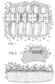
- a micromachined tunable circuit configured as a tunable transmission line 10 is fabricated on a substrate 12 utilizing, for example, thin film integrated circuit manufacturing techniques such as the photoresist, masking, deposition, metalization, selective etching, and chemical milling techniques described in U.S. Patent Application Serial No. 07/608,139, filed on November 1, 1991, by Lawrence E. Larson, and entitled Micro-Machined Switch & Method Of Fabrication .
- thin film integrated circuit manufacturing techniques such as the photoresist, masking, deposition, metalization, selective etching, and chemical milling techniques described in U.S. Patent Application Serial No. 07/608,139, filed on November 1, 1991, by Lawrence E. Larson, and entitled Micro-Machined Switch & Method Of Fabrication .
- other techniques could also be used to fabricate the circuits.
- thin film means films typically deposited by plating, sputtering, evaporation, or vapor deposition and having a typical thickness, by way of example but not limitation, of less than about 10 microns.
- the substrate 12 is made of a dielectric and has a smooth, flat surface 14.
- the substrate is made of gallium-arsenide since it is an excellent dielectric for microwave and millimeter wave applications, and semiconductor devices and passive circuit components can be fabricated on it. It is believed that other materials such as, for example, silicon, sapphire, or indium-phosphide would be appropriate.
- a transmission line 16 is fabricated at the surface 14 of the substrate using photoresist, masking, selective etching, and thin film metalization processes. Specifically, a channel is first etched in the substrate 12 and then metal is deposited into the channel. This segment of the transmission line 16 is generally linear, has a rectangular cross section and has a flat smooth top surface 18 that is coplanar with the plane of the substrate surface 14, as is best illustrated in Fig. 2.
- the transmission line 16 includes a first layer 20 of titanium about 500 A (Angstroms) thick and gold about 4500 A thick deposited by evaporation in the channel. Titanium is used because it bonds very well to gallium arsenide. A layer of gold 22 is plated on top of the layer 20. This gold layer can be about 1 micron thick.
- the width of the transmission line is, for example, 20 to 40 microns and steps down to a narrower width at the right hand side. Of course in some embodiments the transmission line 16 would have the same width along its entire length.
- An array of spaced apart stator control electrodes 26a through 26f are disposed along the transmission line 16 in spaced apart relationship to each other and in spaced electrical isolation from the transmission line. It should be understood that the array of control would extend beyond the control electrode 26f in many embodiments.
- each of the control electrodes such as 26a, is configured as an air bridge that extends over the transmission line 16.
- Two flanges 30 are fabricated on the substrate surface 14 such that each base is adhered to the surface 14 at a location spaced apart from the opposite edges of the transmission line 16. Body portions of the flanges 30 project from the substrate 12 in a plane normal to the surface 14 and parallel to the edges of the transmission line 16.
- a bridge member 36 is fixed to the upper ends of the flanges 30 and extends over the transmission line 16 a sufficient distance so that an air space is created between the upper surface 18 of transmission line 16 and the lower surface of the bridge member 36.
- the control electrodes 26a-26f are fabricated using the previously referenced integrated circuit processing techniques.
- the bases include a layer of titanium about 500 A thick and a layer of gold about 4500 A thick.
- the body portion includes a layer of gold about 3 microns high.
- the bridge member 36 is a layer of gold about 1 micron thick, with a span between flanges 30 of about 100 microns, and a width measured in the direction of the long axis of the transmission line 16 of about 50 microns.
- Each control electrode 26a-26f has a control signal lead 38a-38f, respectively, connected to its bases.
- Each of these control leads is deposited on the substrate surface 14 and extends to a signal pad (not shown) to which a control signal is selectively applied, as will be explained in more detail.
- the control leads each include a thin layer of titanium 500 A thick, a thin layer of gold about 4500 A thick and a thicker layer of gold about 1 micron thick, and is fabricated using the previously referenced processing techniques.
- a ground plane comprised of a plurality of ground plane segments 40 is deposited on the surface 14 in the area between the control leads 38a-38f and spaced from them.
- One edge 42 of each ground plane segment 40 is located in close proximity to the edges of the transmission line 16 but is spaced from the transmission line. This edge 42 is planar and all of the edges 42 are aligned in one of the two planes parallel to each side of the transmission line 16.
- Each of the ground plane segments 40 are connected to a reference voltage level signal commonly referred to as ground potential.
- the ground plane segments 40 are fabricated from the thin layers of titanium and gold and a thicker layer of gold with the thickness of the segments 40 being about 1 micron.
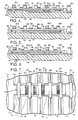
- a movable signal line 50 is positioned on top of the transmission line 16 and is operably moved along the long axis of the transmission line 16 under the influence of electrostatic forces generated by electrostatic control fields of the array of control electrodes 26a through 26f.
- the movable signal line 50 is generally elongate and rectilinear and is formed over the substrate surface 14 such that the signal line's long axis is oriented in the direction of the long axis of the transmission line 16.
- this signal line 50 is configured so that it is not bonded to the substrate 12 or other elements of the tunable circuit 10 when all of the photo resist is removed but is free to move relative to the fixed transmission line 16.
- the signal line 50 is fabricated of the thin layer of titanium and gold and a thicker layer of gold.
- the signal line 50 is, for example, 1 micron thick, 40 microns wide (preferably the width of the transmission line 16), and 300 microns long.
- the side walls 51 of the movable signal line 50 are generally planar and disposed in a plane parallel to the plane of each of the edges 42 of the ground plane segments 40.
- the bottom surface of the signal line 50 closest to the substrate surface 14 has spaced apart node-like bearings 52 formed in it by the previously referred to photoresist and selective etching techniques. These bearings 52 are spaced and configured to ride on the transmission line 16 in low friction sliding relationship. Of course it is possible to eliminate the bearings 52 in certain applications.
- a series of dielectric pads 58 are positioned at spaced apart intervals along the top surface of the movable signal line 50. These dielectric pads 58 are generally rectangular and in the embodiments illustrated have a length in the direction of the long axis of the transmission line about equal to the width of the control electrodes 26a-26f.
- the pads 58 have a dielectric constant greater than ambient air.
- One material that is effective is a 0.2 micron thick layer of silicon dioxide (SiO2) deposited on the surface of the movable signal line using the referenced thin film processes. There is an air gap of between 1.0 and 2.0 microns between the top surface of the dielectric pads 58 and the bottom surface of the bridge member 36.
- each pad 58 is such that at least two of the pads are located under two of the control electrodes 26a-26f at any time. This retains the movable signal line 50 on top of the transmission line 16 during linear translation of the signal line 50.
- a spacing between centers of the adjacent pads 58 in the illustrated embodiments is 3/4 of the corresponding spacing between centers of the adjacent control electrodes 26a-26f. Of course other spacings may also be practical.
- pillar-like stop members 70 are fabricated of metal on the dielectric surface 14 and the transmission line 16 at locations corresponding to the limits of travel. As a result, when the signal line 50 travels to its limits it is stopped by the stops 70 and travel is thus limited.
- control signals A1, A2 and A3 are sequentially applied to the stator control electrodes 26a-26f.
- the control signals A will have a higher or lower voltage potential than ground potential.
- These control signals set up an electrostatic field at each of the control electrodes which develop an electrostatic image charge on the portion of the signal line 50 under the dielectric pads 58 of opposite polarities relative to the dielectric charge on the control electrode above the pad 58.
- the electrostatic attraction between the fields of the control electrodes and the charges on the signal line 50 effectively translate the signal line 50 along the axis of the transmission line 16.
- the sequence of control signal pairs will be A1, A2, A3, A1, A2, etc.
- a control signal sequence A1, A2, A3 applied to the control electrodes will effectively step the signal line 50 to the right. If, however, the signal line 50 is to be stepped from the far right to the left, the sequence of control signals applied to the stator control electrodes 26a-26f will be reversed to A3, A2, A1, A3. As a result of the electrostatic fields and attractions, the signal line 50 translates from right to left to stop in the position illustrated in Fig. 1.
- the signal line 50 can be translated to a position midway between adjacent control electrodes. This is done by simultaneously applying two control signals pairs such as A2 to electrode 26b, and control signal A3 to electrode 26c. The equilibrium point for the electrostatic attraction between the control electrodes and the image changes on the signal line 50 is thus between the adjacent control electrodes. Consequently the signal line 50 comes to rest midway between such adjacent control electrodes.
- Even finer tuning of the signal line 50 can be performed by selectively applying control signals such as A2 and A3 of different amplitudes to adjacent pairs of the control electrodes.
- control signals such as A2 and A3 of different amplitudes
- the equilibrium point of the electrostatic field will positioned nearer to one of the adjacent control electrodes than the other one. For example, if the control signal A3 has a higher amplitude than the control signal A2, the equilibrium point will be closer to the control electrodes to which the higher amplitude control signal A3 is applied.
- the characteristic impedance and effective length of the transmission line is tuned to more closely match the impedances of the circuitry to which the transmission line 16 is coupled.
- a microwave switch 80 is illustrated in Fig. 4.
- a segment of the channel that receives the transmission line 16 is not etched out of the substrate 12.
- This segment 82 thus provides electrical isolation between an input section 84 and an output section 86 of the transmission line 16.
- control signals A1, A2, A3, selectively applied to the control electrodes 26a through 26f translate the signal line 50, which now acts as a switch blade, along the axis of the transmission line sections 82 and 84 to open and close the circuit of switch 80.
- the signal line 50 spans the entire width of the dielectric segment 82 and electrically contacts both the input section 84 of the transmission line and the output section 86. This thus closes the switch circuit by allowing a transmitted signal to be conducted from the input section 84, through the signal line 50, to the output section 86.
- variable attenuator 90 is illustrated in which a segment of the channel that receives the fixed transmission line 16 is filled with a layer of electrical attenuator or resistor material 92.
- This resistor 92 is a layer of nickel and chrome or tantalum 1.0 microns thick and 50 microns wide sputtered into the channel.
- the top surface of the resistor material 92 is smooth and coplanar with the substrate surface 14.
- the movable signal line 50 which now operates as a wiper arm or pick-off for the variable attenuator 90, is operably translated along the axis of the transmission line input section 94 and output section 96.
- control signals A1, A2, A3, etc. are selectively applied to the control electrodes 26a-26f, the movable signal line 50 is stepped across the resistor segment 92.
- the more the signal line 50 extends across the resistor 92 the lower the resistance will be and the less the transmitted signal will be attenuated.
- the resistance will essentially be at 0 ohms.
- a combination switch and variable resistor 100 is fabricated using the above referenced processes.
- a gap between the transmission line input section 102 and an output section 104 is partially filled with the resistor material 106 and partially filled with a segment 108 of the dielectric of the substrate 12.
- control signals A1, A2, A3 selectively applied to the control electrodes 26a-26f move the signal line 50 across the gap between the input and output sections 102 and 104. This varies the resistance of the circuit 100 and attenuates the transmitted signal when the end of the signal line is positioned over the resistor material 106. However, when the signal line 50 is translated to the right, past the dielectric segment 106, the circuit path is opened and the transmitted signal is no longer conducted through the signal line 50 to the output section 104.
- a stub tuner 110 such as the embodiment illustrated in Fig. 7 can be fabricated that incorporates features described herein. Specifically, a coplanar transmission line 112 is formed in a substrate 114 such that the top surface of the transmission line 112 and the substrate surface are coplanar. In addition, a fixed stub 116 is deposited in the substrate such that its top surface is coplanar with the substrate surface. This fixed stub is connected to the transmission line 16 and extends at a right angle to the long axis of the transmission line 112.
- a movable signal line which operates as a movable tuning stub 118, is fabricated over the substrate 114.
- This movable tuning stub which is rectilinear, also has its long axis oriented at a right angle to the axis of the transmission line 112 and is positioned in part over the fixed stub 116.
- the bottom surface of the movable stub 118 is smooth and rides along the smooth top surface of the fixed stub 116 along an axis of movement that is at a right angle to the axis of the transmission line 112. Together the fixed stub 116 and the movable stub 118 form a variable length tuning stub 120.
- a series of spaced apart dielectric pads 122 similar to the pads 58 of Fig. 1, are deposited on the top surface of the movable tuning stub 118 and operate in the same manner as these dielectric pads in the preceding embodiments.
- the movable tuning stub 118 is translated linearly along its axis of movement. This repositioning of the movable stub 118 effectively lengthens and shortens the combined length of the tuning stubs. As a result, the characteristic impedance and effective length of the transmission line 112 is tuned to more closely match the impedances of the circuitry to which it is coupled.
- each of the transmission lines, the tunable stubs, and the stator control electrodes are preferably fabricated of electrically conductive materials such as a thin layer of titanium and gold and thicker layers of gold, each patterned on the substrate using layers of photoresist patterned by masking, photoexposure, selective etching, and metalization.
Description
Claims (12)
- A miniature circuit comprising:characterized bya substrate (12; 114;)first circuit means (16; 84, 86; 92-96; 102-108; 112, 116) fixed thereto; andsecond circuit means (50, 58; 118, 120) disposed over a first portion of said first circuit means (16; 84, 86; 92-96; 102-108; 112, 116) and being movable relative to said first circuit means (16; 84, 86; 92-96; 102-108; 112, 116)control means including control electrodes (26a-26f) having at least one air bridge member (36) disposed to span a portion of said first and said second circuit means (16; 84, 86; 92-96; 102-108; 112, 116; 50, 58; 118, 120) with an air gap therebetween, said control means being operable to effect electrostatic field attraction between said control electrodes (26a-26f) and said second circuit means (50, 58; 118, 120) in response to control signals to move said second circuit means (50, 58; 118, 120) through the air gap and along said first portion of said first circuit means (16; 84, 86; 92-96; 102-108; 112, 116).
- The circuit of claim 1, characterized in that said first portion of said first circuit means (16) is a transmission line.
- The circuit of claim 1 or 2, characterized in that said second circuit means (50, 58) includes at least one dielectric member (58) disposed thereon at a location that operably moves under said at least one air bridge member (36), said at least one dielectric member (58) being operable to effect an image charge on said second circuit means (50, 58) in response to electrostatic field attraction of said air bridge member (36).
- The circuit of any of claims 1 - 3, characterized in that said first circuit means (16; 84, 86; 92-96; 102-108; 112, 116) includes a ground plane means (40) disposed adjacent to said first portion of said first circuit means (16; 84, 86; 92-96; 102-108; 112, 116), said ground plane means (40) being operable to be coupled to said first circuit means (16; 84, 86; 92-96; 102-108; 112, 116) by an electrical field therebetween.
- The circuit of claim 4, characterized in that said control means includes control signal leads (38a-38f) disposed on the substrate (12) and connected to said air bridge member (36), and said ground plane members (40) includes a plurality of segments each disposed between said control signal leads (38a-38f) and said air bridge members (36) in electrical isolation therefrom.
- The circuit of any of claims 1 - 5, characterized in that a surface (18) of said first portion of said first circuit means (16; 84, 86; 92-96; 102-108; 112, 116) is coplanar with a top surface (14) of said substrate (12).
- The circuit of any of claims 2 - 6, characterized in that said transmission line includes an input section (84) and an output section (86) separated from each other by a dielectric means (82), said second circuit means (50) being operable to slide into and out of contact with said dielectric means (82) to operably switch open and closed an electrical circuit path between said input and output sections (84, 86).
- The circuit of any of claims 2 - 6, characterized in that said transmission line includes an input section (94) and an output section (96) separated from each other by an electrical resistor means (92), said second circuit means (50) being operable to slide across said electrical resistor means (92) to vary the resistance of an electrical circuit path that includes said input section (94), said electrical resistor means (92), said second circuit means (50), and said output section (96) and variably attenuate signals transmitted along the circuit path.
- The circuit of any of claims 2 - 6, characterized in that said transmission line includes an input section (102) and an output section (104) separated from each other by an electrical resistor means (106) and a dielectric means (108), said second circuit means (50) being operable to slide across said electrical resistor means (106) and said dielectric means (108) to vary the impedance of and open and close a circuit path that includes said input section (102), said electrical resistor means (106) and said second circuit means (50).
- The circuit of any of claims 1 or 3 - 6, characterized in that said first circuit means (112, 116) includes a transmission line (112) and said first portion of said first circuit means includes a tuning stub (116) fixed to said transmission line (112), and said second circuit means (118, 120) is operable to vary the effective length of said tuning stub (116) as it moves on said first portion.
- The circuit of any of claims 1 - 10, characterized in that said control means includes a plurality of spaced apart air bridge members (36) disposed along said first circuit means (16; 84, 86; 92-96; 102-108; 112, 116), said air bridge members (36) being responsive to control signals applied thereto to operably move said second circuit means (50, 58; 118, 120) by electrostatic field forces,
wherein, preferably, said second circuit means (50, 58) includes at least one dielectric member (58) disposed thereon at a location that operably moves under said at least one air bridge member (36), each of said dielectric members (58) being spaced apart a distance different than the distance between said air bridge members (36) such that at least two of said dielectric members (58) are located under at least two of said air bridge members (36) during movement of said second circuit means (50, 58; 118, 120). - The circuit of any of claims 1 - 11, characterized in that said air bridge members (36) include upright members (30) fixed at one end to said substrate (12) adjacent to said first portion of said first circuit means (16; 84, 86; 92-96; 102-108; 112, 116), and a span member fixed to a free end of said upright member (30) and being disposed to span across said first portion.
Applications Claiming Priority (2)
| Application Number | Priority Date | Filing Date | Title |
|---|---|---|---|
| US712028 | 1991-06-07 | ||
| US07/712,028 US5168249A (en) | 1991-06-07 | 1991-06-07 | Miniature microwave and millimeter wave tunable circuit |
Publications (3)
| Publication Number | Publication Date |
|---|---|
| EP0517232A2 EP0517232A2 (en) | 1992-12-09 |
| EP0517232A3 EP0517232A3 (en) | 1994-05-18 |
| EP0517232B1 true EP0517232B1 (en) | 1999-01-13 |
Family
ID=24860504
Family Applications (1)
| Application Number | Title | Priority Date | Filing Date |
|---|---|---|---|
| EP92109507A Expired - Lifetime EP0517232B1 (en) | 1991-06-07 | 1992-06-05 | Improved miniature microwave and millimeter wave tunable circuit |
Country Status (5)
| Country | Link |
|---|---|
| US (1) | US5168249A (en) |
| EP (1) | EP0517232B1 (en) |
| JP (1) | JPH0795647B2 (en) |
| DE (1) | DE69228146T2 (en) |
| IL (1) | IL102123A (en) |
Families Citing this family (33)
| Publication number | Priority date | Publication date | Assignee | Title |
|---|---|---|---|---|
| US5194833A (en) * | 1991-11-15 | 1993-03-16 | Motorola, Inc. | Airbridge compensated microwave conductors |
| FR2704357B1 (en) * | 1993-04-20 | 1995-06-02 | Thomson Csf | Integrated electronic elements with variable electrical characteristics, in particular for microwave frequencies. |
| US5619061A (en) * | 1993-07-27 | 1997-04-08 | Texas Instruments Incorporated | Micromechanical microwave switching |
| US5467068A (en) * | 1994-07-07 | 1995-11-14 | Hewlett-Packard Company | Micromachined bi-material signal switch |
| US5901031A (en) * | 1995-02-01 | 1999-05-04 | Murata Manufacturing Co., Ltd. | Variable capacitor |
| US5578976A (en) † | 1995-06-22 | 1996-11-26 | Rockwell International Corporation | Micro electromechanical RF switch |
| US5757319A (en) * | 1996-10-29 | 1998-05-26 | Hughes Electronics Corporation | Ultrabroadband, adaptive phased array antenna systems using microelectromechanical electromagnetic components |
| US5994982A (en) * | 1997-07-18 | 1999-11-30 | Trw Inc. | MEMS switched resonators for VCO applications |
| KR100252009B1 (en) * | 1997-09-25 | 2000-04-15 | 윤종용 | Micro structure for oscillation and method of controlling resonant frequency and the same and microactuator and micro gyroscope using the same |
| US6037719A (en) * | 1998-04-09 | 2000-03-14 | Hughes Electronics Corporation | Matrix-addressed display having micromachined electromechanical switches |
| US6724125B2 (en) | 1999-03-30 | 2004-04-20 | Massachusetts Institute Of Technology | Methods and apparatus for diffractive optical processing using an actuatable structure |
| US6329738B1 (en) | 1999-03-30 | 2001-12-11 | Massachusetts Institute Of Technology | Precision electrostatic actuation and positioning |
| KR100320190B1 (en) * | 1999-05-17 | 2002-01-10 | 구자홍 | Structure of rf switch and fabricating method thereof |
| US6143997A (en) | 1999-06-04 | 2000-11-07 | The Board Of Trustees Of The University Of Illinois | Low actuation voltage microelectromechanical device and method of manufacture |
| US6218911B1 (en) * | 1999-07-13 | 2001-04-17 | Trw Inc. | Planar airbridge RF terminal MEMS switch |
| US6215644B1 (en) | 1999-09-09 | 2001-04-10 | Jds Uniphase Inc. | High frequency tunable capacitors |
| US6373682B1 (en) | 1999-12-15 | 2002-04-16 | Mcnc | Electrostatically controlled variable capacitor |
| US6229684B1 (en) | 1999-12-15 | 2001-05-08 | Jds Uniphase Inc. | Variable capacitor and associated fabrication method |
| US6496351B2 (en) | 1999-12-15 | 2002-12-17 | Jds Uniphase Inc. | MEMS device members having portions that contact a substrate and associated methods of operating |
| DE10009453A1 (en) * | 2000-02-29 | 2002-04-04 | Daimler Chrysler Ag | Phase shifter is in form of micromechanical switch whose insulation layer thickness is selected depending on connected phase displacement |
| US6485273B1 (en) | 2000-09-01 | 2002-11-26 | Mcnc | Distributed MEMS electrostatic pumping devices |
| US6590267B1 (en) | 2000-09-14 | 2003-07-08 | Mcnc | Microelectromechanical flexible membrane electrostatic valve device and related fabrication methods |
| US6377438B1 (en) | 2000-10-23 | 2002-04-23 | Mcnc | Hybrid microelectromechanical system tunable capacitor and associated fabrication methods |
| US20020167695A1 (en) * | 2001-03-02 | 2002-11-14 | Senturia Stephen D. | Methods and apparatus for diffractive optical processing using an actuatable structure |
| US7046410B2 (en) | 2001-10-11 | 2006-05-16 | Polychromix, Inc. | Actuatable diffractive optical processor |
| US6919784B2 (en) | 2001-10-18 | 2005-07-19 | The Board Of Trustees Of The University Of Illinois | High cycle MEMS device |
| US6717496B2 (en) | 2001-11-13 | 2004-04-06 | The Board Of Trustees Of The University Of Illinois | Electromagnetic energy controlled low actuation voltage microelectromechanical switch |
| WO2003052781A1 (en) * | 2001-12-14 | 2003-06-26 | Midwest Research Institute | Tunable circuit for tunable capacitor devices |
| US6998946B2 (en) | 2002-09-17 | 2006-02-14 | The Board Of Trustees Of The University Of Illinois | High cycle deflection beam MEMS devices |
| US7753072B2 (en) | 2004-07-23 | 2010-07-13 | Afa Controls Llc | Valve assemblies including at least three chambers and related methods |
| US20070194239A1 (en) * | 2006-01-31 | 2007-08-23 | Mcallister Abraham | Apparatus and method providing a hand-held spectrometer |
| CN103354429B (en) * | 2013-03-12 | 2015-09-16 | 北京纳米能源与系统研究所 | A kind of sliding friction nano generator and electricity-generating method |
| CN108933544B (en) * | 2018-07-02 | 2024-03-12 | 青岛天工智造创新科技有限公司 | Compression device and compression device control method |
Family Cites Families (7)
| Publication number | Priority date | Publication date | Assignee | Title |
|---|---|---|---|---|
| US4096453A (en) * | 1977-05-19 | 1978-06-20 | Gte Automatic Electric Laboratories Incorporated | Double-mode tuned microwave oscillator |
| US4472690A (en) * | 1982-06-14 | 1984-09-18 | Rockwell International Corporation | Universal transistor characteristic matching apparatus |
| US4716389A (en) * | 1986-10-20 | 1987-12-29 | Honeywell Inc. | Millimeter wave microstrip surface mounted attenuator |
| US4906956A (en) * | 1987-10-05 | 1990-03-06 | Menlo Industries, Inc. | On-chip tuning for integrated circuit using heat responsive element |
| US4922253A (en) * | 1989-01-03 | 1990-05-01 | Westinghouse Electric Corp. | High attenuation broadband high speed RF shutter and method of making same |
| JPH0691754B2 (en) * | 1989-04-24 | 1994-11-14 | 新技術事業団 | Contact electrostatic actuator using film |
| US5043043A (en) * | 1990-06-22 | 1991-08-27 | Massachusetts Institute Of Technology | Method for fabricating side drive electrostatic micromotor |
-
1991
- 1991-06-07 US US07/712,028 patent/US5168249A/en not_active Expired - Lifetime
-
1992
- 1992-06-05 DE DE69228146T patent/DE69228146T2/en not_active Expired - Lifetime
- 1992-06-05 EP EP92109507A patent/EP0517232B1/en not_active Expired - Lifetime
- 1992-06-05 IL IL10212392A patent/IL102123A/en not_active IP Right Cessation
- 1992-06-08 JP JP4147645A patent/JPH0795647B2/en not_active Expired - Lifetime
Also Published As
| Publication number | Publication date |
|---|---|
| IL102123A (en) | 1994-08-26 |
| IL102123A0 (en) | 1993-01-14 |
| JPH0795647B2 (en) | 1995-10-11 |
| DE69228146T2 (en) | 1999-05-20 |
| EP0517232A2 (en) | 1992-12-09 |
| EP0517232A3 (en) | 1994-05-18 |
| DE69228146D1 (en) | 1999-02-25 |
| US5168249A (en) | 1992-12-01 |
| JPH05315816A (en) | 1993-11-26 |
Similar Documents
| Publication | Publication Date | Title |
|---|---|---|
| EP0517232B1 (en) | Improved miniature microwave and millimeter wave tunable circuit | |
| EP0516174B1 (en) | Miniature microwave and millimeter wave tuner | |
| EP0516166B1 (en) | Miniature dynamically tunable microwave and millimeter wave device | |
| US7085121B2 (en) | Variable capacitance membrane actuator for wide band tuning of microstrip resonators and filters | |
| US6232847B1 (en) | Trimmable singleband and tunable multiband integrated oscillator using micro-electromechanical system (MEMS) technology | |
| US5696662A (en) | Electrostatically operated micromechanical capacitor | |
| US6898450B2 (en) | High temperature superconducting tunable filter with an adjustable capacitance gap | |
| US6218911B1 (en) | Planar airbridge RF terminal MEMS switch | |
| US6486511B1 (en) | Solid state RF switch with high cutoff frequency | |
| US8436698B2 (en) | MEMS-based tunable filter | |
| US20050099252A1 (en) | RF-MEMS switch and its fabrication method | |
| US20070047173A1 (en) | Low cost digital variable capacitor | |
| US20040229440A1 (en) | Micro-actuator, variable optical attenuator provided with micro-actuator and method for manufacturing the same | |
| EP1227534B1 (en) | Small-sized phase shifter and method of manufacture thereof | |
| WO2014031920A1 (en) | Switches for use in microelectromechanical and other systems, and processes for making same | |
| JPS6125313A (en) | Step variable attenuator |
Legal Events
| Date | Code | Title | Description |
|---|---|---|---|
| PUAI | Public reference made under article 153(3) epc to a published international application that has entered the european phase |
Free format text: ORIGINAL CODE: 0009012 |
|
| AK | Designated contracting states |
Kind code of ref document: A2 Designated state(s): DE FR GB IT |
|
| PUAL | Search report despatched |
Free format text: ORIGINAL CODE: 0009013 |
|
| AK | Designated contracting states |
Kind code of ref document: A3 Designated state(s): DE FR GB IT |
|
| 17P | Request for examination filed |
Effective date: 19941018 |
|
| 17Q | First examination report despatched |
Effective date: 19961015 |
|
| GRAG | Despatch of communication of intention to grant |
Free format text: ORIGINAL CODE: EPIDOS AGRA |
|
| GRAG | Despatch of communication of intention to grant |
Free format text: ORIGINAL CODE: EPIDOS AGRA |
|
| GRAH | Despatch of communication of intention to grant a patent |
Free format text: ORIGINAL CODE: EPIDOS IGRA |
|
| GRAH | Despatch of communication of intention to grant a patent |
Free format text: ORIGINAL CODE: EPIDOS IGRA |
|
| RAP1 | Party data changed (applicant data changed or rights of an application transferred) |
Owner name: HE HOLDINGS, INC. |
|
| RAP1 | Party data changed (applicant data changed or rights of an application transferred) |
Owner name: HUGHES ELECTRONICS CORPORATION |
|
| GRAA | (expected) grant |
Free format text: ORIGINAL CODE: 0009210 |
|
| AK | Designated contracting states |
Kind code of ref document: B1 Designated state(s): DE FR GB IT |
|
| PG25 | Lapsed in a contracting state [announced via postgrant information from national office to epo] |
Ref country code: IT Free format text: LAPSE BECAUSE OF FAILURE TO SUBMIT A TRANSLATION OF THE DESCRIPTION OR TO PAY THE FEE WITHIN THE PRE;WARNING: LAPSES OF ITALIAN PATENTS WITH EFFECTIVE DATE BEFORE 2007 MAY HAVE OCCURRED AT ANY TIME BEFORE 2007. THE CORRECT EFFECTIVE DATE MAY BE DIFFERENT FROM THE ONE RECORDED.SCRIBED TIME-LIMIT Effective date: 19990113 |
|
| ET | Fr: translation filed | ||
| REF | Corresponds to: |
Ref document number: 69228146 Country of ref document: DE Date of ref document: 19990225 |
|
| PLBE | No opposition filed within time limit |
Free format text: ORIGINAL CODE: 0009261 |
|
| STAA | Information on the status of an ep patent application or granted ep patent |
Free format text: STATUS: NO OPPOSITION FILED WITHIN TIME LIMIT |
|
| 26N | No opposition filed | ||
| REG | Reference to a national code |
Ref country code: GB Ref legal event code: IF02 |
|
| PGFP | Annual fee paid to national office [announced via postgrant information from national office to epo] |
Ref country code: FR Payment date: 20110630 Year of fee payment: 20 |
|
| PGFP | Annual fee paid to national office [announced via postgrant information from national office to epo] |
Ref country code: GB Payment date: 20110620 Year of fee payment: 20 |
|
| PGFP | Annual fee paid to national office [announced via postgrant information from national office to epo] |
Ref country code: DE Payment date: 20110622 Year of fee payment: 20 |
|
| REG | Reference to a national code |
Ref country code: DE Ref legal event code: R071 Ref document number: 69228146 Country of ref document: DE |
|
| REG | Reference to a national code |
Ref country code: DE Ref legal event code: R071 Ref document number: 69228146 Country of ref document: DE |
|
| REG | Reference to a national code |
Ref country code: GB Ref legal event code: PE20 Expiry date: 20120604 |
|
| PG25 | Lapsed in a contracting state [announced via postgrant information from national office to epo] |
Ref country code: DE Free format text: LAPSE BECAUSE OF EXPIRATION OF PROTECTION Effective date: 20120606 |
|
| PG25 | Lapsed in a contracting state [announced via postgrant information from national office to epo] |
Ref country code: GB Free format text: LAPSE BECAUSE OF EXPIRATION OF PROTECTION Effective date: 20120604 |