EP0519692A2 - Thin film transistor and method for manufacturing the same - Google Patents
Thin film transistor and method for manufacturing the same Download PDFInfo
- Publication number
- EP0519692A2 EP0519692A2 EP92305529A EP92305529A EP0519692A2 EP 0519692 A2 EP0519692 A2 EP 0519692A2 EP 92305529 A EP92305529 A EP 92305529A EP 92305529 A EP92305529 A EP 92305529A EP 0519692 A2 EP0519692 A2 EP 0519692A2
- Authority
- EP
- European Patent Office
- Prior art keywords
- semiconductor layer
- protective layer
- channel protective
- thin film
- film transistor
- Prior art date
- Legal status (The legal status is an assumption and is not a legal conclusion. Google has not performed a legal analysis and makes no representation as to the accuracy of the status listed.)
- Ceased
Links
- 239000010409 thin film Substances 0.000 title claims abstract description 27
- 238000000034 method Methods 0.000 title claims description 9
- 238000004519 manufacturing process Methods 0.000 title claims description 7
- 239000010410 layer Substances 0.000 claims abstract description 80
- 239000004065 semiconductor Substances 0.000 claims abstract description 61
- 239000010408 film Substances 0.000 claims abstract description 45
- 239000011241 protective layer Substances 0.000 claims abstract description 26
- 239000012535 impurity Substances 0.000 claims abstract description 15
- 239000000758 substrate Substances 0.000 claims abstract description 14
- 238000005468 ion implantation Methods 0.000 claims description 8
- VYPSYNLAJGMNEJ-UHFFFAOYSA-N Silicium dioxide Chemical compound O=[Si]=O VYPSYNLAJGMNEJ-UHFFFAOYSA-N 0.000 claims description 5
- 229910004205 SiNX Inorganic materials 0.000 claims description 4
- 239000004973 liquid crystal related substance Substances 0.000 claims description 3
- 229910052681 coesite Inorganic materials 0.000 claims description 2
- 229910052906 cristobalite Inorganic materials 0.000 claims description 2
- 239000000377 silicon dioxide Substances 0.000 claims description 2
- 235000012239 silicon dioxide Nutrition 0.000 claims description 2
- 229910052682 stishovite Inorganic materials 0.000 claims description 2
- 229910052905 tridymite Inorganic materials 0.000 claims description 2
- 238000002360 preparation method Methods 0.000 abstract 1
- 230000001681 protective effect Effects 0.000 description 27
- 150000002500 ions Chemical class 0.000 description 9
- 229910021417 amorphous silicon Inorganic materials 0.000 description 5
- 239000011159 matrix material Substances 0.000 description 4
- 239000010936 titanium Substances 0.000 description 4
- 229910052782 aluminium Inorganic materials 0.000 description 3
- 238000000151 deposition Methods 0.000 description 3
- 238000005268 plasma chemical vapour deposition Methods 0.000 description 3
- 229910052719 titanium Inorganic materials 0.000 description 3
- 150000001875 compounds Chemical class 0.000 description 2
- 238000005530 etching Methods 0.000 description 2
- 239000011521 glass Substances 0.000 description 2
- 229910052751 metal Inorganic materials 0.000 description 2
- 239000002184 metal Substances 0.000 description 2
- 229910052750 molybdenum Inorganic materials 0.000 description 2
- 238000004544 sputter deposition Methods 0.000 description 2
- ZOKXTWBITQBERF-UHFFFAOYSA-N Molybdenum Chemical compound [Mo] ZOKXTWBITQBERF-UHFFFAOYSA-N 0.000 description 1
- 229910020489 SiO3 Inorganic materials 0.000 description 1
- RTAQQCXQSZGOHL-UHFFFAOYSA-N Titanium Chemical compound [Ti] RTAQQCXQSZGOHL-UHFFFAOYSA-N 0.000 description 1
- XLOMVQKBTHCTTD-UHFFFAOYSA-N Zinc monoxide Chemical compound [Zn]=O XLOMVQKBTHCTTD-UHFFFAOYSA-N 0.000 description 1
- XAGFODPZIPBFFR-UHFFFAOYSA-N aluminium Chemical compound [Al] XAGFODPZIPBFFR-UHFFFAOYSA-N 0.000 description 1
- PNEYBMLMFCGWSK-UHFFFAOYSA-N aluminium oxide Inorganic materials [O-2].[O-2].[O-2].[Al+3].[Al+3] PNEYBMLMFCGWSK-UHFFFAOYSA-N 0.000 description 1
- 229910052787 antimony Inorganic materials 0.000 description 1
- 229910052785 arsenic Inorganic materials 0.000 description 1
- 229910052804 chromium Inorganic materials 0.000 description 1
- 229910052593 corundum Inorganic materials 0.000 description 1
- 238000001312 dry etching Methods 0.000 description 1
- 238000005401 electroluminescence Methods 0.000 description 1
- AMGQUBHHOARCQH-UHFFFAOYSA-N indium;oxotin Chemical compound [In].[Sn]=O AMGQUBHHOARCQH-UHFFFAOYSA-N 0.000 description 1
- 238000012986 modification Methods 0.000 description 1
- 230000004048 modification Effects 0.000 description 1
- 239000011733 molybdenum Substances 0.000 description 1
- 239000002365 multiple layer Substances 0.000 description 1
- 238000000059 patterning Methods 0.000 description 1
- 229910052698 phosphorus Inorganic materials 0.000 description 1
- 238000000206 photolithography Methods 0.000 description 1
- 229910052697 platinum Inorganic materials 0.000 description 1
- 239000002356 single layer Substances 0.000 description 1
- 229910052715 tantalum Inorganic materials 0.000 description 1
- PBCFLUZVCVVTBY-UHFFFAOYSA-N tantalum pentoxide Inorganic materials O=[Ta](=O)O[Ta](=O)=O PBCFLUZVCVVTBY-UHFFFAOYSA-N 0.000 description 1
- 229910052716 thallium Inorganic materials 0.000 description 1
- BKVIYDNLLOSFOA-UHFFFAOYSA-N thallium Chemical compound [Tl] BKVIYDNLLOSFOA-UHFFFAOYSA-N 0.000 description 1
- 238000001039 wet etching Methods 0.000 description 1
- 229910001845 yogo sapphire Inorganic materials 0.000 description 1
Images


Classifications
-
- H—ELECTRICITY
- H01—ELECTRIC ELEMENTS
- H01L—SEMICONDUCTOR DEVICES NOT COVERED BY CLASS H10
- H01L29/00—Semiconductor devices adapted for rectifying, amplifying, oscillating or switching, or capacitors or resistors with at least one potential-jump barrier or surface barrier, e.g. PN junction depletion layer or carrier concentration layer; Details of semiconductor bodies or of electrodes thereof ; Multistep manufacturing processes therefor
- H01L29/66—Types of semiconductor device ; Multistep manufacturing processes therefor
- H01L29/68—Types of semiconductor device ; Multistep manufacturing processes therefor controllable by only the electric current supplied, or only the electric potential applied, to an electrode which does not carry the current to be rectified, amplified or switched
- H01L29/76—Unipolar devices, e.g. field effect transistors
- H01L29/772—Field effect transistors
- H01L29/78—Field effect transistors with field effect produced by an insulated gate
- H01L29/786—Thin film transistors, i.e. transistors with a channel being at least partly a thin film
- H01L29/78696—Thin film transistors, i.e. transistors with a channel being at least partly a thin film characterised by the structure of the channel, e.g. multichannel, transverse or longitudinal shape, length or width, doping structure, or the overlap or alignment between the channel and the gate, the source or the drain, or the contacting structure of the channel
-
- H—ELECTRICITY
- H01—ELECTRIC ELEMENTS
- H01L—SEMICONDUCTOR DEVICES NOT COVERED BY CLASS H10
- H01L29/00—Semiconductor devices adapted for rectifying, amplifying, oscillating or switching, or capacitors or resistors with at least one potential-jump barrier or surface barrier, e.g. PN junction depletion layer or carrier concentration layer; Details of semiconductor bodies or of electrodes thereof ; Multistep manufacturing processes therefor
- H01L29/66—Types of semiconductor device ; Multistep manufacturing processes therefor
- H01L29/66007—Multistep manufacturing processes
- H01L29/66075—Multistep manufacturing processes of devices having semiconductor bodies comprising group 14 or group 13/15 materials
- H01L29/66227—Multistep manufacturing processes of devices having semiconductor bodies comprising group 14 or group 13/15 materials the devices being controllable only by the electric current supplied or the electric potential applied, to an electrode which does not carry the current to be rectified, amplified or switched, e.g. three-terminal devices
- H01L29/66409—Unipolar field-effect transistors
- H01L29/66477—Unipolar field-effect transistors with an insulated gate, i.e. MISFET
- H01L29/66742—Thin film unipolar transistors
- H01L29/6675—Amorphous silicon or polysilicon transistors
- H01L29/66757—Lateral single gate single channel transistors with non-inverted structure, i.e. the channel layer is formed before the gate
-
- H—ELECTRICITY
- H01—ELECTRIC ELEMENTS
- H01L—SEMICONDUCTOR DEVICES NOT COVERED BY CLASS H10
- H01L29/00—Semiconductor devices adapted for rectifying, amplifying, oscillating or switching, or capacitors or resistors with at least one potential-jump barrier or surface barrier, e.g. PN junction depletion layer or carrier concentration layer; Details of semiconductor bodies or of electrodes thereof ; Multistep manufacturing processes therefor
- H01L29/66—Types of semiconductor device ; Multistep manufacturing processes therefor
- H01L29/66007—Multistep manufacturing processes
- H01L29/66075—Multistep manufacturing processes of devices having semiconductor bodies comprising group 14 or group 13/15 materials
- H01L29/66227—Multistep manufacturing processes of devices having semiconductor bodies comprising group 14 or group 13/15 materials the devices being controllable only by the electric current supplied or the electric potential applied, to an electrode which does not carry the current to be rectified, amplified or switched, e.g. three-terminal devices
- H01L29/66409—Unipolar field-effect transistors
- H01L29/66477—Unipolar field-effect transistors with an insulated gate, i.e. MISFET
- H01L29/66742—Thin film unipolar transistors
- H01L29/6675—Amorphous silicon or polysilicon transistors
- H01L29/66765—Lateral single gate single channel transistors with inverted structure, i.e. the channel layer is formed after the gate
-
- H—ELECTRICITY
- H01—ELECTRIC ELEMENTS
- H01L—SEMICONDUCTOR DEVICES NOT COVERED BY CLASS H10
- H01L29/00—Semiconductor devices adapted for rectifying, amplifying, oscillating or switching, or capacitors or resistors with at least one potential-jump barrier or surface barrier, e.g. PN junction depletion layer or carrier concentration layer; Details of semiconductor bodies or of electrodes thereof ; Multistep manufacturing processes therefor
- H01L29/66—Types of semiconductor device ; Multistep manufacturing processes therefor
- H01L29/68—Types of semiconductor device ; Multistep manufacturing processes therefor controllable by only the electric current supplied, or only the electric potential applied, to an electrode which does not carry the current to be rectified, amplified or switched
- H01L29/76—Unipolar devices, e.g. field effect transistors
- H01L29/772—Field effect transistors
- H01L29/78—Field effect transistors with field effect produced by an insulated gate
- H01L29/786—Thin film transistors, i.e. transistors with a channel being at least partly a thin film
- H01L29/78606—Thin film transistors, i.e. transistors with a channel being at least partly a thin film with supplementary region or layer in the thin film or in the insulated bulk substrate supporting it for controlling or increasing the safety of the device
- H01L29/78618—Thin film transistors, i.e. transistors with a channel being at least partly a thin film with supplementary region or layer in the thin film or in the insulated bulk substrate supporting it for controlling or increasing the safety of the device characterised by the drain or the source properties, e.g. the doping structure, the composition, the sectional shape or the contact structure
-
- H—ELECTRICITY
- H01—ELECTRIC ELEMENTS
- H01L—SEMICONDUCTOR DEVICES NOT COVERED BY CLASS H10
- H01L29/00—Semiconductor devices adapted for rectifying, amplifying, oscillating or switching, or capacitors or resistors with at least one potential-jump barrier or surface barrier, e.g. PN junction depletion layer or carrier concentration layer; Details of semiconductor bodies or of electrodes thereof ; Multistep manufacturing processes therefor
- H01L29/66—Types of semiconductor device ; Multistep manufacturing processes therefor
- H01L29/68—Types of semiconductor device ; Multistep manufacturing processes therefor controllable by only the electric current supplied, or only the electric potential applied, to an electrode which does not carry the current to be rectified, amplified or switched
- H01L29/76—Unipolar devices, e.g. field effect transistors
- H01L29/772—Field effect transistors
- H01L29/78—Field effect transistors with field effect produced by an insulated gate
- H01L29/786—Thin film transistors, i.e. transistors with a channel being at least partly a thin film
- H01L29/78651—Silicon transistors
- H01L29/7866—Non-monocrystalline silicon transistors
- H01L29/78663—Amorphous silicon transistors
- H01L29/78666—Amorphous silicon transistors with normal-type structure, e.g. with top gate
-
- H—ELECTRICITY
- H01—ELECTRIC ELEMENTS
- H01L—SEMICONDUCTOR DEVICES NOT COVERED BY CLASS H10
- H01L29/00—Semiconductor devices adapted for rectifying, amplifying, oscillating or switching, or capacitors or resistors with at least one potential-jump barrier or surface barrier, e.g. PN junction depletion layer or carrier concentration layer; Details of semiconductor bodies or of electrodes thereof ; Multistep manufacturing processes therefor
- H01L29/66—Types of semiconductor device ; Multistep manufacturing processes therefor
- H01L29/68—Types of semiconductor device ; Multistep manufacturing processes therefor controllable by only the electric current supplied, or only the electric potential applied, to an electrode which does not carry the current to be rectified, amplified or switched
- H01L29/76—Unipolar devices, e.g. field effect transistors
- H01L29/772—Field effect transistors
- H01L29/78—Field effect transistors with field effect produced by an insulated gate
- H01L29/786—Thin film transistors, i.e. transistors with a channel being at least partly a thin film
- H01L29/78651—Silicon transistors
- H01L29/7866—Non-monocrystalline silicon transistors
- H01L29/78663—Amorphous silicon transistors
- H01L29/78669—Amorphous silicon transistors with inverted-type structure, e.g. with bottom gate
-
- H—ELECTRICITY
- H01—ELECTRIC ELEMENTS
- H01L—SEMICONDUCTOR DEVICES NOT COVERED BY CLASS H10
- H01L29/00—Semiconductor devices adapted for rectifying, amplifying, oscillating or switching, or capacitors or resistors with at least one potential-jump barrier or surface barrier, e.g. PN junction depletion layer or carrier concentration layer; Details of semiconductor bodies or of electrodes thereof ; Multistep manufacturing processes therefor
- H01L29/66—Types of semiconductor device ; Multistep manufacturing processes therefor
- H01L29/68—Types of semiconductor device ; Multistep manufacturing processes therefor controllable by only the electric current supplied, or only the electric potential applied, to an electrode which does not carry the current to be rectified, amplified or switched
- H01L29/76—Unipolar devices, e.g. field effect transistors
- H01L29/772—Field effect transistors
- H01L29/78—Field effect transistors with field effect produced by an insulated gate
- H01L29/786—Thin film transistors, i.e. transistors with a channel being at least partly a thin film
- H01L29/78651—Silicon transistors
- H01L29/7866—Non-monocrystalline silicon transistors
- H01L29/78672—Polycrystalline or microcrystalline silicon transistor
- H01L29/78675—Polycrystalline or microcrystalline silicon transistor with normal-type structure, e.g. with top gate
Definitions
- the present invention relates to a thin film transistor formed as a switching element on an active matrix substrate, which is used in a shutter array, a liquid crystal display or the like.
- Fig. 4 plan view
- Fig. 5 sectional view taken along a line A-A in Fig. 4
- the thin film transistor comprises a gate electrode 12 and a gate insulating film 13 formed on, for example a transparent insulating substrate 11 in this order, and a semiconductor layer 14 and contact layers (n+a-Si) 16a and 16b, which comprise amorphous silicon (a-Si), formed on the gate insulating film 13 above the gate electrode 12.
- the semiconductor layer 14 and the contact layers 16a and 16b are formed so as to be larger than the semiconductor layer 14 and a part where the semiconductor layer 14 is to be left is covered with a channel protective film 15.
- ion implantation is performed thereon, whereby a part which is not covered with the channel protective film 15 becomes the contact layers 16a and 16b.
- a source electrode 17 and a drain electrode 18 are formed so as to be separated on the channel protective film 15 and the drain electrode 18 is electrically connected to a pixel electrode 19 (referring to Fig. 4).
- the conventional thin film transistor shown in Figs. 4 and 5 has the following problem. That is, as shown in Fig. 5, the semiconductor layer 14 is close to the source electrode 17 only through one end of the channel protective film 15 and the semiconductor layer 14 is also close to the drain electrode 18 only through the other end of the channel protective film 15. Therefore, a leak is generated between the source electrode 17 and the drain electrode 18, so that they are not likely to normally operate. A place where the leak is generated is shown by an arrow in the figure. Since the contact layer (a-Si) hardly exists at this part, a leak can not be prevented.
- a thin film transistor comprises a contact layer, in which an impurity is distributed with low concentration, provided between the semiconductor layer and the source and drain electrodes in order to prevent the leak current from being generating.
- a yield or reliability of the transistor is deteriorated because the number of processing and the number of photomasks are increased.
- a method for manufacturing this transistor a non-linear current generated by contact between electrodes at the source and drain regions and a semiconductor layer of the thin film transistor and an OFF current using a hole as a carrier are removed, whereby the channel of the transistor is shortened (Japanese Opened Patent No. 4566/1991).
- the present invention provides a thin film transistor and its manufacturing method capable of preventing a leak from being generated and also capable of being used in an active matrix type display using a large current flow.
- a gate insulating film is formed so as to cover a gate electrode formed on a substrate, a semiconductor layer forming a channel region is deposited on the gate insulating film, a channel protective layer is formed in the vicinity of the center of the semiconductor layer, and a drain electrode and a source electrode are extended in the right and left directions along the semiconductor layer surface from the right and left sides of the channel protective layer, respectively.
- the channel protective layer has inclined surfaces on its right and left sides and an impurity for preventing a leak current and providing ohmic contact is doped in the semiconductor layer region which is in contact with the source and drain electrodes and in the semiconductor region just under the foot of the inclined surface of the channel protective layer.
- a gate electrode on a substrate, a gate insulating film covering the gate electrode, a semiconductor layer forming a channel region on the gate insulating film, and a cone-shaped channel protective layer provided on the semiconductor layer in the vicinity of the center thereof and comprising inclined right and left side surfaces; an ion doped region is formed in the exposed semiconductor layer and in the semiconductor layer under the foot of the inclined surface of the channel protective layer; and drain and source electrodes extending in the right and left directions along the exposed semiconductor layer from the right and left sides of the channel protective layer, respectively.
- a channel protective film is formed such that its side surface are inclined, a contact layer is formed from the lower part of the inclined surface of the channel protective film over an exposed surface of the semiconductor layer and a semiconductor layer is formed at a part other than the contact layer under the channel protective film. More specifically, the contact layer also exists under the channel protective film. Therefore, there is the contact layer having a sufficient thickness between the semiconductor layer and the source electrode, and the semiconductor layer and the drain electrode. Thus, a distance between the semiconductor layer and the source electrode and a distance between the semiconductor layer and the drain electrode are increased by the contact layers. As a result, a leak current can be prevented from being generated between the source electrode and the drain electrode.
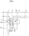
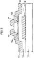
- Fig. 1 is a plan view showing a part of a thin film transistor of the present invention and Fig. 2 is a sectional view taken along a line B-B of Fig. 1.
- a gate electrode 2 is formed on a transparent insulating substrate 1 such as glass (CORNING 7059) or quartz glass. More specifically, the gate electrode 2 is formed by depositing a single-layer or multiple-layer metal having a thickness of 2,000 to 4,000 ⁇ such as Ta, Ti, Al, or Cr on the transparent insulating substrate 1 by sputtering and patterning it. At this time, a gate bus line 2a having the gate electrode 2 which diverges midway is formed (referring to Fig. 1).
- a gate insulating film 3 and a semiconductor layer 4′ are formed on the gate electrode 2 on the substrate 1. More specifically, the gate insulating film 3 is formed by depositing SiN x , Ta2O5, SiO3, Al2O3 or the like by a thickness of 2,000 to 5,000 ⁇ by a plasma CVD method. Then, a semiconductor layer 4′ is formed thereon.
- the semiconductor layer 4′ comprises contact layers 6a and 6b and contact layers 6a′ and 6b′ in which an impurity is implanted with low concentration. These five layers are formed by varying the degree of ion implantation into the semiconductor layer 4′.
- Group (III) atom such as P, As, Sb or Pt is implanted.
- Group (V) atom such as B is implanted. The ion concentration at this time is approximately 1010 to 1017 /cm2.
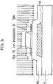
- the semiconductor layer 4′ having a thickness of 200 to 2,000 ⁇ is deposited by for example, a plasma CVD method and patterned and then the channel protective layer 5 having a thickness of 1,000 to 3,000 ⁇ and comprising SiN x , SiO2 or the like is formed on the semiconductor layer 4′ in the same manner as the above.
- a side surface of a resist is inclined by lowering a baking temperature of the resist and the side surface of the channel protective film 5 is inclined by etching the channel protective film 5 while the side surface of the resist retreats by dry etching.
- an etching selection ratio of the channel protective film and the semiconductor layer has a sufficiently large range.
- a resist pattern is formed by a normal photolithography and etched away using BHF or the like, whereby a taper can be easily provided.
- An angle of inclination ⁇ of the side surface of the channel protective film 5 having a cone-shaped section (trapezoid in this example) in which an upper side is shorter than a lower side as shown in Fig. 3 is preferably less than 90° or desirably ranges 10 to 50°. More specifically, the angle of inclination may be set so that an impurity can be implanted into a layer under the channel protective film 5 because a lower part of the protective film is thin by its inclination.
- an impurity of Group (V) element such as P+, PH+, PH2+, B+, As ⁇ or their compound or Group (III) element or their compound is implanted into the semiconductor layer 4′ by ion implantation with an accelerating voltage of 1 to 100keV, desirably 5 to 50 keV.
- the impurity is implanted with high concentration into a part of the semiconductor layer 4′ which is not covered with the channel protective film 5 and then the contact layers 6a and 6b are formed.
- the impurity is implanted with low concentration into a part of the semiconductor layer 4′ which is covered with the inclined side surface of the channel protective film 5 and then the contact layers 6a′ and 6b′ are formed.
- the semiconductor layer 4 into which the impurity is not implanted is formed under the center of the channel protective film 5.
- a source electrode 7 and a drain electrode 8 are formed thereon.
- Each electrode has one end put on the channel protective film 5.
- the electrodes are 2,000 to 4,000 ⁇ in thickness and comprise Ti, Al, Mo, Cr or the like.
- a pixel electrode 9 is formed so as to be in electrically contact with the drain electrode 8.
- the pixel electrode 9 comprises an indium tin oxide (ITO) or zinc oxide (ZnO) film in a case of a transparent type or comprises thallium (Ta), molybdenum (Mo), aluminum (Al) or titanium (Ti) film in a case of a reflection type and has a thickness of 500 to 1,000 ⁇ .
- the thin film transistor is structured as described above, there are contact layers 6a′ and 6b′ in which the impurity is implanted with low concentration under the channel protective film 5 as shown in Fig. 2. Therefore, the semiconductor layer 4 and the source electrode 7, and the semiconductor layer 4 and the drain electrode 8 are separated by the contact layers 6a′ and 6b′ in which the impurity is implanted with low concentration, respectively, whereby a leak current can be prevented from being generated between the source electrode 7 and the drain electrode 8.
- the contact layer is also formed under the side surface of the channel protective film 5 by an ion implantation method in the above embodiment of the present invention, the present invention is not limited to this method and the contact layer may be formed at the same place by another method.
- a thin film transistor was manufactured in accordance with the structure and the manufacturing method as described above.
- glass CORNING 7059
- the gate electrode 2 comprising single-phase metal such as Ta was formed by a thickness of approximately 1200 ⁇ on the substrate 1 by sputtering and then patterned.
- the gate bus line 2a having the gate electrode 2 and diverging midway was formed.
- the gate insulating film 3 and the semiconductor layer 4′ were formed. More specifically, the gate insulating film was formed by depositing SiN x by a thickness of approximately 3000A by a plasma CVD method.
- the semiconductor layer 4′ was formed of amorphous silicon to be an n type semiconductor by implanting P ions.
- the channel protective film 5 was deposited on the semiconductor layer 4′.
- the channel protective film 5 was formed of Sin x and its thickness was approximately 2,000 ⁇ and an angle of inclination ⁇ on the side surface was approximately 30°. Then, P ions were implanted from the above with an accelerating voltage of approximately 30keV. A part of the semiconductor layer 4′ which was not covered with the channel protective film 5 was implanted with ions with high concentration and became contact layers 6a and 6b having an ion concentration of approximately 5 x 10¹⁵/cm2.
- the source electrode 7 and the drain electrode 8 were formed on the substrate 1 such that one end of each of the electrodes was on the channel protective film 5.
- the source electrode 7 and the drain electrode 8 was formed of Mo and were approximately 2,000 ⁇ in thickness.
- the pixel electrode 9 were formed on the substrate 1 so as to be connected to the drain electrode 8.
- the pixel electrode 9 was formed of ITO and was approimately 1,000 ⁇ in thickness.
- the thin film transistor of the present invention since the contact layer in which the impurity is implanted with low concentration exists under the side surface of the channel protective film, a leak current generated between the source electrode and the drain electrode can be reduced by one or two figures. As a result, the leak current can be prevented from being generated.
- the thin film transistor of the above structure can be formed without increasing the number of processing or the number of photomasks. As a result, it can be applied to an active matrix type display which requires a large current flow.
Abstract
a channel protective layer (5) formed on the semiconductor layer in the vicinity of the center thereof; and
a drain electrode (8) and a source electrode (7) extending in the right and left directions along said semiconductor layer surface from the right and left sides of said channel protective layer, respectively,
wherein said channel protective layer has inclined right and left side surfaces, and the semiconductor layer is in contact with said source and drain electrodes and is doped with an impurity just under the foot of the inclined side surfaces of said channel protective layer in order to prevent a leak and to provide ohmic contact and preparation method.
Description
- The present invention relates to a thin film transistor formed as a switching element on an active matrix substrate, which is used in a shutter array, a liquid crystal display or the like.
- Fig. 4 (plan view) and Fig. 5 (sectional view taken along a line A-A in Fig. 4) show a conventional thin film transistor. The thin film transistor comprises a
gate electrode 12 and agate insulating film 13 formed on, for example a transparentinsulating substrate 11 in this order, and asemiconductor layer 14 and contact layers (n⁺a-Si) 16a and 16b, which comprise amorphous silicon (a-Si), formed on thegate insulating film 13 above thegate electrode 12. As shown in Fig. 5, thesemiconductor layer 14 and thecontact layers semiconductor layer 14 and a part where thesemiconductor layer 14 is to be left is covered with a channelprotective film 15. Then, ion implantation is performed thereon, whereby a part which is not covered with the channelprotective film 15 becomes thecontact layers - Next, as shown in Fig. 5, a
source electrode 17 and adrain electrode 18 are formed so as to be separated on the channelprotective film 15 and thedrain electrode 18 is electrically connected to a pixel electrode 19 (referring to Fig. 4). - However, the conventional thin film transistor shown in Figs. 4 and 5 has the following problem. That is, as shown in Fig. 5, the
semiconductor layer 14 is close to thesource electrode 17 only through one end of the channelprotective film 15 and thesemiconductor layer 14 is also close to thedrain electrode 18 only through the other end of the channelprotective film 15. Therefore, a leak is generated between thesource electrode 17 and thedrain electrode 18, so that they are not likely to normally operate. A place where the leak is generated is shown by an arrow in the figure. Since the contact layer (a-Si) hardly exists at this part, a leak can not be prevented. - Especially, although an active matrix type display of large capacity and high density such as an HD (High Definition) TV or a graphic display which uses a liquid crystal or electroluminescence has recently been developed and put to practical use, when the conventional thin film transistor is used in the above display, a leak current of approximately 10⁻⁹ to 10⁻¹¹A is generated and then it sometimes can not be used therein.
- Referring to the above problem, it is proposed that a thin film transistor comprises a contact layer, in which an impurity is distributed with low concentration, provided between the semiconductor layer and the source and drain electrodes in order to prevent the leak current from being generating. However, a yield or reliability of the transistor is deteriorated because the number of processing and the number of photomasks are increased. According to a method for manufacturing this transistor, a non-linear current generated by contact between electrodes at the source and drain regions and a semiconductor layer of the thin film transistor and an OFF current using a hole as a carrier are removed, whereby the channel of the transistor is shortened (Japanese Opened Patent No. 4566/1991).
- The present invention provides a thin film transistor and its manufacturing method capable of preventing a leak from being generated and also capable of being used in an active matrix type display using a large current flow.
- According to the thin film transistor of the present invention, a gate insulating film is formed so as to cover a gate electrode formed on a substrate, a semiconductor layer forming a channel region is deposited on the gate insulating film, a channel protective layer is formed in the vicinity of the center of the semiconductor layer, and a drain electrode and a source electrode are extended in the right and left directions along the semiconductor layer surface from the right and left sides of the channel protective layer, respectively. The channel protective layer has inclined surfaces on its right and left sides and an impurity for preventing a leak current and providing ohmic contact is doped in the semiconductor layer region which is in contact with the source and drain electrodes and in the semiconductor region just under the foot of the inclined surface of the channel protective layer.
- In addition, according to the method for forming the thin film transistor of the present invention, there is formed a gate electrode on a substrate, a gate insulating film covering the gate electrode, a semiconductor layer forming a channel region on the gate insulating film, and a cone-shaped channel protective layer provided on the semiconductor layer in the vicinity of the center thereof and comprising inclined right and left side surfaces; an ion doped region is formed in the exposed semiconductor layer and in the semiconductor layer under the foot of the inclined surface of the channel protective layer; and drain and source electrodes extending in the right and left directions along the exposed semiconductor layer from the right and left sides of the channel protective layer, respectively.
-
- Fig. 1 is a plan view showing a part of a thin film transistor in accordance with the present invention;
- Fig. 2 is a sectional view taken along a line B-B of Fig. 1;
- Fig. 3 is a sectional view showing ion implantation in accordance with the preset invention;
- Fig. 4 is a plan view showing a part of a conventional thin film transistor;
- Fig. 5 is a sectional view taken along a line A-A of Fig. 4; and
- Fig. 6 is a sectional view showing conventional ion implantation.
- According to the present invention, a channel protective film is formed such that its side surface are inclined, a contact layer is formed from the lower part of the inclined surface of the channel protective film over an exposed surface of the semiconductor layer and a semiconductor layer is formed at a part other than the contact layer under the channel protective film. More specifically, the contact layer also exists under the channel protective film. Therefore, there is the contact layer having a sufficient thickness between the semiconductor layer and the source electrode, and the semiconductor layer and the drain electrode. Thus, a distance between the semiconductor layer and the source electrode and a distance between the semiconductor layer and the drain electrode are increased by the contact layers. As a result, a leak current can be prevented from being generated between the source electrode and the drain electrode.
- Fig. 1 is a plan view showing a part of a thin film transistor of the present invention and Fig. 2 is a sectional view taken along a line B-B of Fig. 1. In the thin film transistor, a
gate electrode 2 is formed on a transparentinsulating substrate 1 such as glass (CORNING 7059) or quartz glass. More specifically, thegate electrode 2 is formed by depositing a single-layer or multiple-layer metal having a thickness of 2,000 to 4,000 Å such as Ta, Ti, Al, or Cr on the transparentinsulating substrate 1 by sputtering and patterning it. At this time, agate bus line 2a having thegate electrode 2 which diverges midway is formed (referring to Fig. 1). - A
gate insulating film 3 and asemiconductor layer 4′ are formed on thegate electrode 2 on thesubstrate 1. More specifically, thegate insulating film 3 is formed by depositing SiNx, Ta₂O₅, SiO₃, Al₂O₃ or the like by a thickness of 2,000 to 5,000 Å by a plasma CVD method. Then, asemiconductor layer 4′ is formed thereon. Thesemiconductor layer 4′ comprisescontact layers contact layers 6a′ and 6b′ in which an impurity is implanted with low concentration. These five layers are formed by varying the degree of ion implantation into thesemiconductor layer 4′. - In order to form an n type semiconductor, Group (III) atom, such as P, As, Sb or Pt is implanted. Alternatively, in order to form a p type semiconductor, Group (V) atom such as B is implanted. The ion concentration at this time is approximately 10¹⁰ to 10¹⁷ /cm².
- More specifically, as shown in Fig. 3, the
semiconductor layer 4′ having a thickness of 200 to 2,000 Å is deposited by for example, a plasma CVD method and patterned and then the channelprotective layer 5 having a thickness of 1,000 to 3,000 Å and comprising SiNx, SiO₂ or the like is formed on thesemiconductor layer 4′ in the same manner as the above. - When the protective layer is formed, a side surface of a resist is inclined by lowering a baking temperature of the resist and the side surface of the channel
protective film 5 is inclined by etching the channelprotective film 5 while the side surface of the resist retreats by dry etching. At this time, an etching selection ratio of the channel protective film and the semiconductor layer has a sufficiently large range. In addition, in a case of wet etching, a resist pattern is formed by a normal photolithography and etched away using BHF or the like, whereby a taper can be easily provided. - An angle of inclination Θ of the side surface of the channel
protective film 5 having a cone-shaped section (trapezoid in this example) in which an upper side is shorter than a lower side as shown in Fig. 3 is preferably less than 90° or desirably ranges 10 to 50°. More specifically, the angle of inclination may be set so that an impurity can be implanted into a layer under the channelprotective film 5 because a lower part of the protective film is thin by its inclination. - Then, an impurity of Group (V) element such as P⁺, PH⁺, PH₂⁺, B⁺, As⁻ or their compound or Group (III) element or their compound is implanted into the
semiconductor layer 4′ by ion implantation with an accelerating voltage of 1 to 100keV, desirably 5 to 50 keV. At this time, the impurity is implanted with high concentration into a part of thesemiconductor layer 4′ which is not covered with the channelprotective film 5 and then thecontact layers semiconductor layer 4′ which is covered with the inclined side surface of the channelprotective film 5 and then thecontact layers 6a′ and 6b′ are formed. At the same time, thesemiconductor layer 4 into which the impurity is not implanted is formed under the center of the channelprotective film 5. - Then, a
source electrode 7 and adrain electrode 8 are formed thereon. Each electrode has one end put on the channelprotective film 5. The electrodes are 2,000 to 4,000 Å in thickness and comprise Ti, Al, Mo, Cr or the like. - In addition, a pixel electrode 9 is formed so as to be in electrically contact with the
drain electrode 8. The pixel electrode 9 comprises an indium tin oxide (ITO) or zinc oxide (ZnO) film in a case of a transparent type or comprises thallium (Ta), molybdenum (Mo), aluminum (Al) or titanium (Ti) film in a case of a reflection type and has a thickness of 500 to 1,000 Å. - Since the thin film transistor is structured as described above, there are
contact layers 6a′ and 6b′ in which the impurity is implanted with low concentration under the channelprotective film 5 as shown in Fig. 2. Therefore, thesemiconductor layer 4 and thesource electrode 7, and thesemiconductor layer 4 and thedrain electrode 8 are separated by the contact layers 6a′ and 6b′ in which the impurity is implanted with low concentration, respectively, whereby a leak current can be prevented from being generated between thesource electrode 7 and thedrain electrode 8. - In addition, although the contact layer is also formed under the side surface of the channel
protective film 5 by an ion implantation method in the above embodiment of the present invention, the present invention is not limited to this method and the contact layer may be formed at the same place by another method. - A thin film transistor was manufactured in accordance with the structure and the manufacturing method as described above.
- According to this embodiment of the present invention, glass (CORNING 7059) was used as the transparent insulating
substrate 1 which was approximately 1.1mm in thickness. Thegate electrode 2 comprising single-phase metal such as Ta was formed by a thickness of approximately 1200 Å on thesubstrate 1 by sputtering and then patterned. At the same time, thegate bus line 2a having thegate electrode 2 and diverging midway was formed. - In addition, the
gate insulating film 3 and thesemiconductor layer 4′ were formed. More specifically, the gate insulating film was formed by depositing SiNx by a thickness of approximately 3000A by a plasma CVD method. Thesemiconductor layer 4′ was formed of amorphous silicon to be an n type semiconductor by implanting P ions. In addition, the channelprotective film 5 was deposited on thesemiconductor layer 4′. The channelprotective film 5 was formed of Sinx and its thickness was approximately 2,000 Å and an angle of inclination Θ on the side surface was approximately 30°. Then, P ions were implanted from the above with an accelerating voltage of approximately 30keV. A part of thesemiconductor layer 4′ which was not covered with the channelprotective film 5 was implanted with ions with high concentration and becamecontact layers - Meanwhile, since a part just under the center of the channel
protective film 5 was not implanted with ions, it was still the n type semiconductor layer and its ion concentration was less than 5 x 10¹⁵/cm². The contact layers 6a′ and 6b′ in which ions were implanted with low concentration existed therebetween. - Then, the
source electrode 7 and thedrain electrode 8 were formed on thesubstrate 1 such that one end of each of the electrodes was on the channelprotective film 5. Thesource electrode 7 and thedrain electrode 8 was formed of Mo and were approximately 2,000 Å in thickness. Then, the pixel electrode 9 were formed on thesubstrate 1 so as to be connected to thedrain electrode 8. The pixel electrode 9 was formed of ITO and was approimately 1,000 Å in thickness. - As described above, according to the thin film transistor of the present invention, since the contact layer in which the impurity is implanted with low concentration exists under the side surface of the channel protective film, a leak current generated between the source electrode and the drain electrode can be reduced by one or two figures. As a result, the leak current can be prevented from being generated. In addition, by using the manufacturing method of the present invention, the thin film transistor of the above structure can be formed without increasing the number of processing or the number of photomasks. As a result, it can be applied to an active matrix type display which requires a large current flow.
- While only certain presently preferred embodiments have been described in detail, as will be apparent with those skilled in the art, certain changes and modifications can be made without departing from the scope of the invention as defined by the following claims.
Claims (8)
- A thin film transistor comprising:
a gate electrode formed on a substrate;
a gate insulating film covering said gate electrode;
a semiconductor layer forming a channel region on said gate insulating film;
a channel protective layer formed on the semiconductor layer in the vicinity of the center thereof; and
a drain electrode and a source electrode extending in the right and left directions along said semiconductor layer surface from the right and left sides of said channel protective layer, respectively,
wherein said channel protective layer has inclined right and left side surfaces, and the semiconductor layer is in contact with said source and drain electrodes and is doped with an impurity just under the foot of the inclined side surfaces of said channel protective layer in order to prevent a leak and to provide ohmic contact. - A thin film transistor according to claim 1, wherein an angle of inclination formed by a inclined side surface of the channel protective layer and the semiconductor layer ranges 10 to 50°.
- A thin film transistor according to claim 1 wherein a thickness of the channel protective layer ranges 1000 to 3,000 Å.
- A thin film transistor according to claim 1, wherein the channel protective layer is formed of SiNx or SiO₂.
- A thin film transistor according to claim 1, wherein it is adopted to a liquid crystal display.
- A method for manufacturing a thin film transistor comprising the steps of:
forming a gate electrode on a substrate, a gate insulating film covering said gate electrode, a semiconductor layer on said gate insulating film so that a channel region is formed, and a cone-shaped channel protective layer on the semiconductor layer in the vicinity of the center thereof, the protective layer comprising inclined right and left side surfaces;
forming an ion doped region in the exposed semiconductor layer and the semiconductor layer just under the foot of the inclined side surface by ion implantation of an impurity in order to provide ohmic contact; and
forming a drain electrode and a source electrode extending in the right and left directions along the exposed semiconductor layer from the right and left sides of said channel protective layer, respectively. - A method for manufacturing a thin film transistor according to claim 6, wherein an accelerating voltage of ion implantation of an impurity ranges from 1 to 100 keV.
- A method of forming first and second contact regions (6a, 6b) in spaced apart portions of a semiconductor layer (4) by an ion doping operation, said regions being separated by a protective layer (5) acting as a mask during ion doping, characterised in that said protective layer is formed so as to have inclined side surfaces adjacent to said regions whereby ion doping is effected not only in fully exposed parts of the semiconductor layer adjacent said protective layer (5), but also in portions (6a′, 6b′) lying immediately beneath the foot of each of said inclined side surfaces.
Applications Claiming Priority (2)
| Application Number | Priority Date | Filing Date | Title |
|---|---|---|---|
| JP3144914A JP2634505B2 (en) | 1991-06-17 | 1991-06-17 | Thin film transistor and method of manufacturing the same |
| JP144914/91 | 1991-06-17 |
Publications (2)
| Publication Number | Publication Date |
|---|---|
| EP0519692A2 true EP0519692A2 (en) | 1992-12-23 |
| EP0519692A3 EP0519692A3 (en) | 1993-07-21 |
Family
ID=15373196
Family Applications (1)
| Application Number | Title | Priority Date | Filing Date |
|---|---|---|---|
| EP19920305529 Ceased EP0519692A3 (en) | 1991-06-17 | 1992-06-17 | Thin film transistor and method for manufacturing the same |
Country Status (4)
| Country | Link |
|---|---|
| EP (1) | EP0519692A3 (en) |
| JP (1) | JP2634505B2 (en) |
| KR (1) | KR100288368B1 (en) |
| TW (1) | TW222715B (en) |
Cited By (5)
| Publication number | Priority date | Publication date | Assignee | Title |
|---|---|---|---|---|
| US7223666B2 (en) | 1996-10-31 | 2007-05-29 | Semiconductor Energy Laboratory Co., Ltd. | Semiconductor device that includes a silicide region that is not in contact with the lightly doped region |
| US7799590B2 (en) | 2000-01-26 | 2010-09-21 | Semiconductor Energy Laboratory Co., Ltd. | Semiconductor device and manufacturing method thereof |
| US8120039B2 (en) | 1999-11-19 | 2012-02-21 | Semiconductor Energy Laboratory Co., Ltd. | Semiconductor device |
| US9496292B2 (en) | 2012-06-14 | 2016-11-15 | Japan Display Inc. | Display device and manufacturing method for same |
| US9905702B2 (en) | 2011-09-29 | 2018-02-27 | Semiconductor Energy Laboratory Co., Ltd. | Semiconductor device and method for manufacturing the same |
Families Citing this family (1)
| Publication number | Priority date | Publication date | Assignee | Title |
|---|---|---|---|---|
| JP2014038911A (en) * | 2012-08-13 | 2014-02-27 | Sony Corp | Thin film transistor and manufacturing method of the same, and display device and electronic apparatus |
Citations (1)
| Publication number | Priority date | Publication date | Assignee | Title |
|---|---|---|---|---|
| DE3237539A1 (en) * | 1981-10-14 | 1983-07-21 | Rockwell International Corp., 90245 El Segundo, Calif. | MICROELECTRONIC SHADOW MASKING METHOD FOR REDUCING THE PUNCHTHROUGH |
-
1991
- 1991-06-17 JP JP3144914A patent/JP2634505B2/en not_active Expired - Fee Related
-
1992
- 1992-06-16 TW TW081104711A patent/TW222715B/zh active
- 1992-06-17 EP EP19920305529 patent/EP0519692A3/en not_active Ceased
- 1992-06-17 KR KR1019920010701A patent/KR100288368B1/en not_active IP Right Cessation
Patent Citations (1)
| Publication number | Priority date | Publication date | Assignee | Title |
|---|---|---|---|---|
| DE3237539A1 (en) * | 1981-10-14 | 1983-07-21 | Rockwell International Corp., 90245 El Segundo, Calif. | MICROELECTRONIC SHADOW MASKING METHOD FOR REDUCING THE PUNCHTHROUGH |
Non-Patent Citations (3)
| Title |
|---|
| JAPANESE JOURNAL OF APPLIED PHYSICS PART 2 vol. 30, no. 1A, 1 January 1991, TOKYO JP pages L67 - L69 , XP223826 AKIHISA YOSHIDA ET AL 'Fabrication of a-Si:H Thin Film Transistors on 4-inch Glass Substrates by a Large Area Ion Doping Technique' * |
| JAPANESE JOURNAL OF APPLIED PHYSICS, SUPPLEMENTS (1991)AUGUST 27-29 TOKYO JA pages 608 - 610 , XP279507 YASUHIRO MITANI ET AL 'The Switching Characteristics of a-Si TFT Fabricated by Ion Doping Technique' * |
| PATENT ABSTRACTS OF JAPAN vol. 015, no. 114 (E-1047)19 March 1991 & JP-A-30 04 566 ( NEC CORP ) 10 January 1991 * |
Cited By (13)
| Publication number | Priority date | Publication date | Assignee | Title |
|---|---|---|---|---|
| US7993992B2 (en) | 1996-10-31 | 2011-08-09 | Semiconductor Energy Laboratory Co., Ltd. | Semiconductor device and method of fabricating the same |
| US7622740B2 (en) | 1996-10-31 | 2009-11-24 | Semiconductor Energy Laboratory Co., Ltd. | Semiconductor device and method of fabricating the same |
| US7223666B2 (en) | 1996-10-31 | 2007-05-29 | Semiconductor Energy Laboratory Co., Ltd. | Semiconductor device that includes a silicide region that is not in contact with the lightly doped region |
| US8957424B2 (en) | 1999-11-19 | 2015-02-17 | Semiconductor Energy Laboratory Co., Ltd. | Electroluminescence display device |
| US8120039B2 (en) | 1999-11-19 | 2012-02-21 | Semiconductor Energy Laboratory Co., Ltd. | Semiconductor device |
| US8569767B2 (en) | 1999-11-19 | 2013-10-29 | Semiconductor Energy Laboratory Co., Ltd. | Electroluminescence display device |
| US8729557B2 (en) | 1999-11-19 | 2014-05-20 | Semiconductor Energy Laboratory Co., Ltd. | Electroluminescence display device |
| US9673223B2 (en) | 1999-11-19 | 2017-06-06 | Semiconductor Energy Laboratory Co., Ltd. | Electroluminescence display device |
| US8017456B2 (en) | 2000-01-26 | 2011-09-13 | Semiconductor Energy Laboratory Co., Ltd. | Semiconductor device and manufacturing method thereof |
| US8513666B2 (en) | 2000-01-26 | 2013-08-20 | Semiconductor Energy Laboratory Co., Ltd. | Semiconductor device and manufacturing method thereof |
| US7799590B2 (en) | 2000-01-26 | 2010-09-21 | Semiconductor Energy Laboratory Co., Ltd. | Semiconductor device and manufacturing method thereof |
| US9905702B2 (en) | 2011-09-29 | 2018-02-27 | Semiconductor Energy Laboratory Co., Ltd. | Semiconductor device and method for manufacturing the same |
| US9496292B2 (en) | 2012-06-14 | 2016-11-15 | Japan Display Inc. | Display device and manufacturing method for same |
Also Published As
| Publication number | Publication date |
|---|---|
| KR100288368B1 (en) | 2001-10-24 |
| JPH04369229A (en) | 1992-12-22 |
| TW222715B (en) | 1994-04-21 |
| EP0519692A3 (en) | 1993-07-21 |
| JP2634505B2 (en) | 1997-07-30 |
| KR930001502A (en) | 1993-01-16 |
Similar Documents
| Publication | Publication Date | Title |
|---|---|---|
| US5371398A (en) | Thin film transistor | |
| KR100225098B1 (en) | Method of fabrication of thin transistor | |
| US5371025A (en) | Method of making thin film transistors | |
| US4700458A (en) | Method of manufacture thin film transistor | |
| US6992435B2 (en) | Thin film transistor, organic electroluminescence display device and manufacturing method of the same | |
| US5648674A (en) | Array circuitry with conductive lines, contact leads, and storage capacitor electrode all formed in layer that includes highly conductive metal | |
| US5712494A (en) | Thin film field effect transistor having an extension portion acting as a light shield and back gate | |
| US6410411B1 (en) | Electronic device and their manufacture | |
| US5391507A (en) | Lift-off fabrication method for self-aligned thin film transistors | |
| US6051883A (en) | Manufacturing method and semiconductor device with low contact resistance between transparent electrode and pad electrode | |
| US5751020A (en) | Structure of a liquid crystal display unit having exposed channel region | |
| US6309903B2 (en) | Method for manufacturing fringe field switching mode liquid crystal display device | |
| JPH0629534A (en) | Manufacture of metal wiring | |
| EP0721215B1 (en) | Forming array with metal scan lines to control semiconductor gatelines | |
| JPH09232448A (en) | Thin film transistor and its manufacture | |
| GB2169746A (en) | Thin film transistor | |
| US5693567A (en) | Separately etching insulating layer for contacts within array and for peripheral pads | |
| EP0641028B1 (en) | A thin film device and a method for fabricating the same | |
| EP0519692A2 (en) | Thin film transistor and method for manufacturing the same | |
| KR100209623B1 (en) | Liquid crystal display device and its manufacturing method | |
| JP2719252B2 (en) | Thin film transistor | |
| CA1305398C (en) | Method for producing high yield electrical contacts to n _amorphous silicon | |
| JP3419073B2 (en) | Thin film transistor, method of manufacturing the same, and active matrix liquid crystal display device | |
| JPH08181319A (en) | Thin-film transistor and its manufacture | |
| JP2002523898A (en) | Thin film transistor and method of manufacturing the same |
Legal Events
| Date | Code | Title | Description |
|---|---|---|---|
| PUAI | Public reference made under article 153(3) epc to a published international application that has entered the european phase |
Free format text: ORIGINAL CODE: 0009012 |
|
| AK | Designated contracting states |
Kind code of ref document: A2 Designated state(s): DE FR GB NL |
|
| PUAL | Search report despatched |
Free format text: ORIGINAL CODE: 0009013 |
|
| AK | Designated contracting states |
Kind code of ref document: A3 Designated state(s): DE FR GB NL |
|
| 17P | Request for examination filed |
Effective date: 19931102 |
|
| 17Q | First examination report despatched |
Effective date: 19941201 |
|
| STAA | Information on the status of an ep patent application or granted ep patent |
Free format text: STATUS: THE APPLICATION HAS BEEN REFUSED |
|
| 18R | Application refused |
Effective date: 19970130 |