EP0526930A1 - A processor buffered interface for multiprocessor systems - Google Patents
A processor buffered interface for multiprocessor systems Download PDFInfo
- Publication number
- EP0526930A1 EP0526930A1 EP92202127A EP92202127A EP0526930A1 EP 0526930 A1 EP0526930 A1 EP 0526930A1 EP 92202127 A EP92202127 A EP 92202127A EP 92202127 A EP92202127 A EP 92202127A EP 0526930 A1 EP0526930 A1 EP 0526930A1
- Authority
- EP
- European Patent Office
- Prior art keywords
- data
- address
- processor
- memory
- microprocessor
- Prior art date
- Legal status (The legal status is an assumption and is not a legal conclusion. Google has not performed a legal analysis and makes no representation as to the accuracy of the status listed.)
- Withdrawn
Links
- 230000015654 memory Effects 0.000 claims abstract description 240
- 230000008878 coupling Effects 0.000 claims abstract description 20
- 238000010168 coupling process Methods 0.000 claims abstract description 20
- 238000005859 coupling reaction Methods 0.000 claims abstract description 20
- 230000004044 response Effects 0.000 claims abstract description 11
- 239000000872 buffer Substances 0.000 claims description 125
- 238000004891 communication Methods 0.000 claims description 17
- 238000012545 processing Methods 0.000 claims description 17
- 230000003139 buffering effect Effects 0.000 claims description 7
- 238000013500 data storage Methods 0.000 claims 32
- 230000003213 activating effect Effects 0.000 claims 2
- 230000006870 function Effects 0.000 abstract description 27
- 238000010586 diagram Methods 0.000 description 18
- 230000007704 transition Effects 0.000 description 11
- 238000012546 transfer Methods 0.000 description 8
- 230000007246 mechanism Effects 0.000 description 4
- 238000000034 method Methods 0.000 description 4
- 230000002457 bidirectional effect Effects 0.000 description 2
- 238000012937 correction Methods 0.000 description 2
- 230000001934 delay Effects 0.000 description 2
- 230000009977 dual effect Effects 0.000 description 2
- 230000007274 generation of a signal involved in cell-cell signaling Effects 0.000 description 2
- 230000008569 process Effects 0.000 description 2
- 238000000638 solvent extraction Methods 0.000 description 2
- 238000012800 visualization Methods 0.000 description 2
- 238000013459 approach Methods 0.000 description 1
- 238000003491 array Methods 0.000 description 1
- 230000008901 benefit Effects 0.000 description 1
- 230000001143 conditioned effect Effects 0.000 description 1
- 238000010276 construction Methods 0.000 description 1
- 238000012217 deletion Methods 0.000 description 1
- 230000037430 deletion Effects 0.000 description 1
- 238000001514 detection method Methods 0.000 description 1
- 238000005516 engineering process Methods 0.000 description 1
- 238000007667 floating Methods 0.000 description 1
- 238000011010 flushing procedure Methods 0.000 description 1
- 230000002452 interceptive effect Effects 0.000 description 1
- 238000003672 processing method Methods 0.000 description 1
- 238000012163 sequencing technique Methods 0.000 description 1
- 230000011664 signaling Effects 0.000 description 1
- 238000004088 simulation Methods 0.000 description 1
- 230000001360 synchronised effect Effects 0.000 description 1
- 230000036962 time dependent Effects 0.000 description 1
- 230000000007 visual effect Effects 0.000 description 1
Images


Classifications
-
- G—PHYSICS
- G06—COMPUTING; CALCULATING OR COUNTING
- G06F—ELECTRIC DIGITAL DATA PROCESSING
- G06F13/00—Interconnection of, or transfer of information or other signals between, memories, input/output devices or central processing units
- G06F13/38—Information transfer, e.g. on bus
- G06F13/42—Bus transfer protocol, e.g. handshake; Synchronisation
- G06F13/4204—Bus transfer protocol, e.g. handshake; Synchronisation on a parallel bus
- G06F13/4208—Bus transfer protocol, e.g. handshake; Synchronisation on a parallel bus being a system bus, e.g. VME bus, Futurebus, Multibus
- G06F13/4217—Bus transfer protocol, e.g. handshake; Synchronisation on a parallel bus being a system bus, e.g. VME bus, Futurebus, Multibus with synchronous protocol
-
- G—PHYSICS
- G06—COMPUTING; CALCULATING OR COUNTING
- G06F—ELECTRIC DIGITAL DATA PROCESSING
- G06F12/00—Accessing, addressing or allocating within memory systems or architectures
- G06F12/02—Addressing or allocation; Relocation
- G06F12/08—Addressing or allocation; Relocation in hierarchically structured memory systems, e.g. virtual memory systems
- G06F12/0802—Addressing of a memory level in which the access to the desired data or data block requires associative addressing means, e.g. caches
- G06F12/0806—Multiuser, multiprocessor or multiprocessing cache systems
- G06F12/0815—Cache consistency protocols
- G06F12/0831—Cache consistency protocols using a bus scheme, e.g. with bus monitoring or watching means
- G06F12/0835—Cache consistency protocols using a bus scheme, e.g. with bus monitoring or watching means for main memory peripheral accesses (e.g. I/O or DMA)
-
- G—PHYSICS
- G06—COMPUTING; CALCULATING OR COUNTING
- G06F—ELECTRIC DIGITAL DATA PROCESSING
- G06F15/00—Digital computers in general; Data processing equipment in general
- G06F15/16—Combinations of two or more digital computers each having at least an arithmetic unit, a program unit and a register, e.g. for a simultaneous processing of several programs
- G06F15/163—Interprocessor communication
- G06F15/17—Interprocessor communication using an input/output type connection, e.g. channel, I/O port
Definitions
- This invention relates generally to multiprocessor data processing systems and, in particular, to method and apparatus for interfacing each of the processors to common, or shared, system resources and also to local, or private, processor resources.
- System requirements needed to interact with and visualize large, time-dependent data sets include a large, high-bandwidth disk array to store the entire data set being processed, a high speed network to download a problem set, a large, high-speed memory to buffer all data required to process a single simulation time step, computational power that is adequate to manipulate, enhance, and visualize the data sets, and a real-time, high resolution visual display. Furthermore, it is important that these functions be provided within a highly programmable and flexible user environment.
- An important consideration in a multiprocessor system is the interfacing of each of the processors to common, or shared, system resources and also to local, or private, processor resources. As an example, it may be required to interface each processor to a global bus having a system memory coupled thereto, while also coupling each processor to a private memory.
- Bus interface unit for distributing the control of data transfers within single instruction stream, multiple data stream processors.
- Bus interface units 13, 14, 15 are each connected between local memories (18, 19, 20), respectively, and a main bus 10 having a main memory 16 connected thereto through a bus interface unit 12.
- control channel interface for interfacing a processor to a time division multiplexed (TDM) bus.
- TDM time division multiplexed
- Each CCI is polled by a master processor to determine if the CCI has information to send.
- a CCI may buffer information until it can dispose of the information after being polled.
- the MPIF includes a dual ported RAM which can function as a FIFO, under the control of one processor, or as a shared memory.
- microprocessor-controlled circuit for interconnecting at least two very high speed integrated circuit chips having digital inputs and outputs.
- the circuit includes a local data bus, a microprocessor and associated memory, and a plurality of functional interface units.
- One functional interface unit is connected between the microprocessor and a local memory bus.
- each processor of a multiprocessor system including both computational and I/O processors, with an interface unit for coupling the processor to a private and to a shared memory, the interface unit further including control circuitry controlling the operation of a one line cache, external to the processor, that buffers read and write data passing between the processor and the shared memory.
- the invention teaches interface circuitry for coupling to a microprocessor device.
- the interface circuitry includes an input for coupling to the microprocessor device for receiving address signal lines and control signal lines generated by the microprocessor device.
- the interface further includes an address decoder, responsive to the received address signal lines, for determining if a microprocessor-generated memory access is directed to a private memory, accessible only by the microprocessor device, or to a shared memory that is accessible by a plurality of microprocessor devices. Responsive to the address decoder, the interface circuitry provides first address signal lines and first control signal lines to the private memory in response to the microprocessor device generating a memory access to the private memory means. Also responsive to the address decoder, the interface circuitry provides second address signal lines and second control signal lines for coupling to the shared memory in response to the microprocessor device generating a memory access to the shared memory.
- the interface circuitry of the invention is particularly useful in a multiprocessor embodiment wherein a plurality of processor devices share a common memory over a high speed system or global bus.
- the interface circuitry provides both a local (private) memory interface and a shared memory interface for an associated processor.
- the interface circuitry also provides a number of additional functions including interrupt control, inter-processor interrupt capability, and direct memory access functions for transferring data between the shared memory and the private memory.
- the interface circuitry also provides a number of miscellaneous functions such as programmable timer/counters, processor reset logic, and private memory refresh control.
- the interface circuitry also includes circuitry for interfacing to a serial diagnostic bus.
- the interface circuitry furthermore manages external read and write buffers that are interposed between a processor node data bus and the global data bus.
- the read and write buffers function in a manner similar to a one line cache and serve to reduce the bandwidth requirements of the global bus.
- FIG. 1 there is illustrated a multiprocessor system that includes a serial diagnostic bus and controller that is constructed and operated in accordance with the invention. Specifically, there are illustrated components of a Scientific Visualization System (SVS) 10.
- SVS 10 Scientific Visualization System
- a purpose of the SVS 10 is to process, manipulate, and visualize complex data sets at interactive speeds, although the use of the system 10 is not limited to only this one important application.
- the use of the processor interface of the invention is not restricted to only this particular system. That is, the processor interface as taught by the invention may be employed to advantage in a number of different types of multiprocessor systems.
- the SVS 10 includes several major components.
- a first component is a server 12 embodied within a data processing system that provides large-scale computational power, high-speed memory, and intelligent I/O processors, all of which are interconnected by a high speed global bus.
- the terms global bus, shared bus, and common interconnect are used interchangeably herein.
- a second component is a console processor 14 embodied in, by example, a RISC System/6000 (RS/6000) workstation manufactured by the International Business Machines Corporation (RISC System/6000 is a Trademark of the International Business Machines Corporation).
- the console 14 provides network access from remote workstations (not shown) and interfaces with the serial diagnostic controller of the invention in a manner described below.
- a third component is a Frame buffer 16 that includes, by example, an RS/6000 workstation that provides console functions therefor.
- the frame buffer 16 includes interface and image buffering hardware 16a attached via an ANSI standard High Performance Parallel Interface (HIPPI) interface for providing real-time display capability to high-resolution displays 18.
- HIPPI High Performance Parallel Interface
- a further component of the system 10 is a disk array 20.
- the disk array 20 may be embodied within a storage system having 21 GByte capacity with 55 MByte/second transfer rate via a HIPPI interface.
- Server 12 is comprised of a plurality of individual processors 22a organized as four processors (P1-P4) per printed circuit card 22.
- the server 12 may include up to eight cards for a total of 32 processors.
- Each processor card 22 includes a universal bus interface (UBIF) 34 for coupling a Local Processor Card (LPC) bus 32 to an SVS global bus 24.
- LPC Local Processor Card
- SVS global bus 24 Also coupled to the SVS global bus 24 are a plurality of Global Memory cards 26, a plurality of I/O processor cards 28, and an interface 30 to the RS/6000 console 14.
- each processor card 22 includes up to four processor nodes each having a microprocessor 22a.
- each microprocessor 22a is an i860-type device, specifically an 80860 microprocessor device manufactured by Intel Corporation (i860 is a Trademark of the Intel Corporation).
- a local node bus 23 comprised of a local node data bus 23a, a local node address bus 23b, and a local node control bus 23c, is a local node memory 22b providing, in this embodiment, 16 megabytes (MB) of storage.
- MB 16 megabytes
- Each processor node also includes, in accordance with the invention, a Processor Buffered Interface (PBIF) 22c, which incorporates an interface to the LPC bus 32. Additionally, each processor node includes an interface 22d (seen in Fig. 2) to a serial bus (S).
- PBIF Processor Buffered Interface
- S serial bus
- one of the processor cards 22 is capable of a peak performance of 160 million instructions per second (MIPS), or 320 million single precision floating point operations per second (MFLOPS).
- MIPS 160 million instructions per second
- MFLOPS single precision floating point operations per second
- a fully configured system of eight processor cards 22 provides a peak performance approaching 1.28 billion instructions per second (BIPS) or 2.56 GFLOPS, assuming 40 MHz operation.
- each of the Global Memory cards 26 is configured with either 128 MB or 256 MB of random access memory with error correction logic.
- the server 12 may include up to four Global Memory cards 26.
- Each of the Global Memory cards 26 provides a data bandwidth of 640 MB/second in a manner that reduces a memory access latency seen by each processor in the system 10. This is accomplished by partitioning the Global Memory on each memory card 26 into four memory banks (BO-B3), each of which is capable of independently performing block read cycles, page mode read or write cycles and random read or write cycles.
- a Global Memory Card (GMC) bus 26a enables each of the banks (BO-B3) to operate independently, while utilizing common global bus resources.
- the I/O processor cards 28 each include a processor node 28a, similar to the processor card 22, plus two HIPPI receivers 28b, and two HIPPI transmitters 28C. Each IOP 28 provides four HIPPI interfaces, each of which is capable of operation at a transfer rate of 100 MB/second. Each IOP 28 includes a dedicated processor node 28a, such as is found on the processor card 22, having a microprocessor coupled to 16MB of local memory. Two receiver channels 28b and two transmitter channels 28c are provided on each IOP 28. The channels may operate independently to deliver 100 Mbytes/second each, or in a paired manner to deliver 200 Mbytes/second.
- the HIPPI interfaces are employed to support high speed disk arrays, provide real-time images to HIPPI-attached frame buffers, and realize high speed communication with external devices, such as supercomputers.
- the Console interface 30 is partitioned into two cards, one which is found within the server 12 and one which resides in the console 14.
- the link between the two card allows access to the SVS server global memory and serial bus, which in turn allows access to each processor's local memory and PBIF.
- the system 10 also includes an Arbiter 36 that is coupled to the Global Bus 24 and which operates to arbitrate requests for the Global Bus between the processors 22, the memory 26, console interface 30, and the I/O processors 28.
- Arbiter 36 that is coupled to the Global Bus 24 and which operates to arbitrate requests for the Global Bus between the processors 22, the memory 26, console interface 30, and the I/O processors 28.
- the Global Bus 24 is implemented with Emitter Coupled Logic (ECL) technology for interconnecting these various components and providing a 1.28 GB/sec transfer rate.
- ECL Emitter Coupled Logic
- Appendix A describes the various Global Bus 24 signal lines.
- Major signal groups of the Global Bus 24 include a 32-bit address bus (ABUS) 24a, a 256-bit data bus (DBUS) 24b, and a control bus.
- Each SVS 10 server 12 supports up to 12 master devices (i.e. processor cards 22, I/O processor cards 28, or Interface card 30), and up to four memory cards 26.
- One configuration includes an Interface card 30, eight processor cards 22 (or 32 processors), four Global Memory cards 26 each with 256 MBytes of storage for a total of 1024 MB of high speed memory, and one I/O processor 28 to support the high speed disk array 20, receive data from a HIPPI source, and distribute image data to HIPPI attached frame buffers 16.
- the console 14 provides a user interface to the SVS 10 as well as support for standard I/O devices.
- each component card of the system 10 includes one of the UBIFs 34.
- the UBIF 34 presents a shared, synchronous, decoupled interface to the Global Bus 24, provides local arbitration on the LPC bus 32 or GMC bus 26a, and performs all necessary handshaking and retry sequencing with the Global bus 24.
- the UBIF 34 provides bidirectional, pipelined buffering to support up to four local master devices, such as processors 22a, or up to four slave devices, such as the memory banks B1-B4.
- the UBIF 34 supports data bus widths between eight bits and 256 bits and provides a peak data transfer rate of 1.28 Gbytes/second between the Local Bus 32 and the Global Bus 24, assuming 40 MHz bus operation (25 nanosecond bus cycle).
- the PBIF 22c functions as an interface and a control device for the associated computational processor 22a or I/O processor 28a.
- the PBIF 22c provides all of the required logic, with the exception of tranceivers and memory, to interface a high performance microprocessor to a high performance multi-processor system.
- the PBIF 22c functions in an identical manner with each of the I/O processors 28a.
- the PBIF 22c architecture is implemented as a set of discrete data registers together with an Application Specific Integrated Circuit (ASIC).
- ASIC Application Specific Integrated Circuit
- Each PBIF 22c provides control and address generation for up to 32 MBytes of local memory 22b.
- Each PBIF 22c provides control signals to an external 256-bit wide read and write buffer 22e to cache Global Memory 26 operations.
- Each PBIF 22c provides support for up to eight externally generated interrupts and eight internally generated interrupts.
- Each PBIF 22c provides support for an inter-processor interrupt mechanism whereby a processor in the system can interrupt any other processor (or group of processors).
- Each PBIF 22c provides a means of transferring data at high speed between the Global Memory 26 and the associated Local Memory 22b using direct memory access cycles.
- Each PBIF 22c incorporates a Control and Status Register (CSR), two programmable timer/counters, logic to reset the associated processor 22a or 28a, and other functions, as will be described.
- CSR Control and Status Register
- Each PBIF 22c includes circuitry that works in concert with a serial diagnostic bus, as described in European patent application 92 109 675.6 (IBM Docket No. YO 991 042).
- FIG. 4 A block diagram of the PBIF 22c, showing the partitioning of the device into these functional blocks, is shown in Fig. 4.
- PBIF 22c includes a plurality of state machines, including a Control/Status Register (CSR) state machine 78, a local memory state machine 52, and a global memory state machine 54. These three state machines have inputs connected to the control and address signal lines of the attached processor 22a or 28a.
- the global memory state machine 54 receives an input from a DMA controller 56 and an interprocessor communication (IPC) register 58.
- the local memory state machine 52 generates local memory address and control signal lines that are coupled to the local memory 22b for controlling accesses thereto.
- the global memory state machine 54 generates global memory address and control signal lines that are coupled via the local processor bus 32 and the UBIF 34 to the global bus 24.
- the global memory state machine 54 generates global memory address and control signals in response to the local processor 22a or 28a or in response to the operation of the DMA controller 56 or the IPC register 58.
- the DMA controller 56 further includes a source address register 56a, a destination address register 56b, and a length/blocksize register 56c. These registers are loaded by the attached processor for controlling DMA operations.
- the source address register 56a is initially loaded with the memory address from which data is to be read
- the destination address register 56b is initially loaded with the address to which the data is to be stored
- the length/blocksize register 56c is initially loaded with a value representing a number of data units that are to be transferred during a DMA operation.
- PBIF 22c also includes a timer/counter register 60a and a time stamp register 60b.
- the PBIF 22c also includes a control status register 62, the operation of which is described in further detail below.
- the PBIF 22c includes a block of interrupt-related registers. These include an interrupt register 64a which latches incoming interrupts and then, in turn, interrupts the processor 22a, as appropriate.
- the PBIF 22c further includes an interrupt mask register 64b, a clear interrupt register 64c, and a memory fault address register 64d.
- a refresh register 66 is provided for controlling the refresh timing parameters for the local memory 22b DRAMs.
- the aforementioned IPC register 58 has an associated send interrupt register 68.
- the serial diagnostic controller 70 is described in the aforementioned European patent application 92 109 675.6 (IBM Docket No. YO 991 042).
- the aforementioned registers 56 through 68 are all bidirectionally coupled to the local processor through a data multiplexer 72 such that the local processor is enabled to store information within and read information from these registers.
- Fig. 5 shows in greater detail the construction of the PBIF 22c and also shows in greater detail the input and output signal lines. Specifically, the outputs of the local memory state machine 52 and the global memory state machine 54 are shown in greater detail.
- the block diagram of Fig. 5 also shows several other state machines including a reset state machine 74, a LED state machine 76, and the CSR state machine 78.
- the serial diagnostic controller 70 can be seen to include a serial state machine 70a, an address register 70b and a data register 70c all of which are connected in series and have an output connected to a serial out signal line that is threaded through each of the PBIFs within the system 10.
- Fig. 6 shows in greater detail the interconnection, within a local processor node, of the PBIF 22c to the local processor 22a (or 28a), the local memory 22b, the global memory interface 22e, and the local bus 32.
- the local memory 22b is partitioned into 8 Mbyte banks and also includes a parity memory section for storing parity memory information associated with each of the memory banks.
- a set of eight registered transceivers 22f is employed for bidirectionally interfacing the memory banks and parity memory to the local node 64-bit data bus 23a.
- a set of eight transceivers 22g bidirectionally couple the local node data bus 23a to the read and write buffers of the global memory interface 22e.
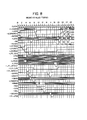
- Fig. 7 is a timing diagram showing the global memory 26 write timing that is generated by the global memory state machine 54. Signal names shown in Fig. 7 correspond to the signal designations of Fig. 5 and are described in Appendix B. Global Bus 24 signal designators are described in Appendix A. LPC bus 32 signal designators are described in Appendix C.
- Fig. 8 is a timing diagram that depicts global memory 26 read timing that is generated by the global memory state machine 54. It should be noted that the global memory read and write timing includes local memory 22b signal generation, as provided by the local memory state machine 52, and local bus 32 signal generation.
- Figs. 9 and 10 show in greater detail the operation of the IPC portion of the PBIF 22c. Specifically, Fig. 9 shows the IPC register 58 format and the coupling of the IPC register 58 to the local bus 32 and to the global bus 24. Fig. 10 shows in greater detail the IPC logic 80, particularly an IPC cycle detection logic block 80a and an IPC processor selection logic block 80b.
- the PBIF 22c provides all of the required logic, with the exception of tranceivers and memory, to interface a high performance microprocessor to a high performance multi- processor system. These functions are now described in greater detail below.
- the local memory 22b interface includes an address multiplexer 82 that provides both the address multiplexing for row and column addresses, and also the local memory state machine 52 that generates control signals required to interface to up to 32 MBytes of local memory 22b. This capability is based on the number of multiplexed address lines which this particular implementation of the PBIF 22c generates. Other embodiments may provide access to more or less than 32 MBytes of local memory.
- the PBIF 22c also provides a programmable refresh rate for the local memory 22b.
- the refresh register 66 is written with a divisor that is applied to the system clock. The resulting divided clock is used to periodically generate refresh cycles. Any refresh request is queued until all currently executing memory cycles are complete. The pending refresh request then has priority over any new cycles requested by the processor 22a. Local memory 22b refresh occurs unhindered if the processor 22a is accessing another range in memory (such as Global Memory 26).
- the processor 22a for this embodiment of the invention, includes an internal 8 KB data cache and a 4 KB instruction cache having cache lines that are 256-bits in width, and an external data bus that is 64 bits in width.
- the width of the internal cache line coincides with the width of the Global Data Bus (DBUS 24b), although the width of the processor 22a data bus is a factor of four less than that of DBUS 24b.
- the two external 256-bit registers 22e provide data bus width matching, and also provide an external, one line, level two cache for the processor 22a.
- the address is decoded within the PBIF 22c by address decode block 84 and the relevant request lines to the UBIF 34 (which controls the Global Bus 24) are generated.
- the PBIF 22c drives the address onto the LPC bus 32, along with any necessary control lines.
- the PBIF 22c then "snoops" the local bus 32, waiting for the Global Memory 26 data to be returned.
- the PBIF 22c When data is returned to an identified processor from the Global Memory 26, the PBIF 22c generates control signals to latch the returned data into the external read buffer 86, and then enables the appropriate word (64-bits) back to the identified processor 22a via the local node data bus 23a. If the processor 22a follows the first request with another request to a 64-bit word, which is also encached within the 256-bit read buffer 86, the second 64-bit word is returned to the processor 22a from the read buffer 86 with minimal latency, and without utilizing any bus bandwidth on either of the shared busses (LPC 32 and GB 24).
- the shared busses LPC 32 and GB 24
- the global memory state machine 54 is optimized to support cache reloads, where consecutive words are loaded into the processor 22a. After the initial latency for the first Global Memory 26 read, all subsequent words are returned in two bus cycles.
- Various address comparison functions are performed within the PBIF 22c with registers 90a and 90b and comparators 92a, 92b, 92c, and 94.
- Registers 90a and 90b maintain a record of the addresses of words that are currently stored in the external buffers 22e. If an out-of-sequence read is requested from the buffer 86 (i.e. the least significant 64-bits followed by the most significant 64-bits), an additional cycle is allowed for bus turnaround, and the read requires three cycles to complete. Reference is again made to the timing diagrams for Global Memory 26 reads (Fig. 8) and writes (Fig. 7).
- the contents of the read buffer 86 are invalidated if the processor 22a requests a word which is not currently cached, or if the currently cached word is detected as being written on the Global Bus 24.
- the PBIF 22c snoops all bus cycles on the Global Bus 24 to determine if a write takes place to a location in Global Memory 26 which is currently encached within the associated read buffer 86. This snooping function is accomplished with comparator 94.
- some conditions result in an invalidation of the read buffer 86. For example, a read from the processor 22a, with N10_LOCK active, invalidates the current contents of the read buffer 86, and the data is instead fetched from GM 26. However, this condition may be disabled via a Control Status Register 62 bit.
- Another signal line (LPC_NOCACHE) on the local bus 32 enables external devices to signal that they are returning non-cacheable data. Also, if a processor 22a writes the same address as is currently cached for reads, the read buffer 86 is invalidated. Furthermore, as a fail safe mechanism, the read buffer 86 may be automatically invalidated by the PBIF 22c after 256 reads of the same encached data, without a read buffer 86 reload from Global Memory 26. This feature is controlled by a bit in the CSR 62. The combination of these features ensures that any data stored within the read buffer 86 remains consistent with the copy stored within Global Memory 26.
- the write buffer 88 operates in a similar fashion.
- the processor 22a writes a word to a Global Memory 26 location, it is cached in the write buffer 88. Any further writes within the same 256-bits are stored within the write buffer 88.
- the write buffer 88 circuitry includes a register 88b for storing processor 22a byte enables, and updates these buffered write enables as appropriate. If the processor 22a writes to a location that is not currently cached in the write buffer 88 the contents of the write buffer 88 are flushed out to Global Memory 26, with the PBIF 22c generating the appropriate control signals, and the newly written word replaces the old within the write buffer 88.
- a software-controllable mode enables the write buffer 88 to be written out to Global Memory 26 after all 32 bytes have been written by the associated processor 22a.
- the write buffer 88 is also flushed if the processor 22a issues a locked write to Global Memory 26.
- a locked write is a special type of write cycle which the processor 22a may execute. During locked memory cycles, only the processor which initiated the lock is allowed to alter the data which it locked. This ensures consistency in multiprocessor systems, where many processors may attempt to share the same data.
- the processor 22a indicates a locked cycle by enabling a special output pin (N10_LOCK) during the cycle. If a locked write is requested to Global Memory 26, this condition first flushes the present contents of the write buffer 88, so as to maintain order, and then writes the locked word without buffering it. This operation is similar to that previously described for locked reads.
- a read of a Global Memory 26 address which is currently buffered in the write buffer 88 causes the write buffer 88 to be flushed before the read request is issued. This ensures that if the copy of the data in the write buffer 88 is more current than that contained within the Global Memory 26, that the most current version is returned to the requesting processor.
- the PBIF 22c also implements timeout mechanisms for all shared bus accesses.
- the 32-bit local bus address corresponds to a 256-bit data address
- the most significant five address bits are programmable, via a segment register in the PBIF 22c, to allow 128 Gbytes of Global Memory 26 to be addressed.
- the PBIF 22c supports up to eight external, level-sensitive interrupts and eight internally generated interrupts.
- the interrupts are individually maskable through the interrupt mask register 64b, and individually clearable through the clear interrupt register 64c. Any active, non-masked interrupts are OR'd together and passed through to the single interrupt input pin of the processor 22a.
- the Memory Fault Address Register (MFAR) 64d stores the last three addresses accessed by the processor 22a, and in the event of a parity, ECC or bus error interrupt, enables the failing address to be read.
- Timer/Counter Interrupt This interrupt is set after the timer/counter 60a is initialized to a starting value and subsequently decrements to zero.
- This interrupt is set when the PBIF 22c receives a request from the processor 22a to an address which is not mapped.
- This interrupt is set when the PBIF 22c receives an interrupt packet over the serial diagnostic interface bus.
- Buserror Interrupt This interrupt is set when the PBIF 22c times out while attempting to access the local bus 32.
- This interrupt is set at the completion of a DMA operation.
- two pins (+ LPC - ECCERR--I and + LPC - ERRTYPE--I) are implemented on the PBIF 22c and are used as interrupt inputs for indicating ECC errors returned with data read from Global Memory 26.
- the PBIF 22c contains two registers 58 and 68 which support the sending of inter-processor interrupts.
- the IPC register 58 is differentiated into a Processor Select Mask register 58a and a GSI register 58b.
- the Processor Select Mask register 58a (Fig. 9) defines a destination mask and has a width of 32-bits, with each bit being associated with one of the system 10 processors. This enables a processor to send an interrupt to any one processor, or group of processors, within the system.
- An additional four bits stored within the GSI register 58b select a destination system unit, or the type of processor (computation or I/O).
- the second register is the Send Interrupt Register 68 (Fig. 4) which controls the dispatch of the interrupt.
- a processor may also interrupt itself via this mechanism.
- the IPC interrupt is performed as a special local bus 32 cycle.
- the PBIF 22c sends an IPC interrupt message as a special read cycle that is differentiated from a normal read cycle by means of an extra pin on the local bus, LPC_ATYPE.
- This special local bus read cycle is passed through to the Global Bus 24 by the associated UBIF 34, and is decoded (Fig. 10) by the UBIF on any card which has its specific identifier set in the destination field.
- the LPC bus address lines, LPC_A(31:0) are used to convey the 32- bit processor 22a mask, and the length field, LPC_LEN(3:0), is used to convey the additional descriptor information.
- the UBIF 34 on any card which decodes a valid bit in the destination field generates the signal IPCINTR(3:0) to interrupt the relevant processor(s).
- the PBIF 22c supports Block DMA between the Global Memory 26 and the associated local memory 22b by means of the source address register 56a, the destination address register 56b, and the length/blocksize register 56c.
- the Global bus 24 supports block data transfers, both the size of the blocks to be transferred and the number of blocks are specified. Returned data blocks are stored in the UBIF 34 until requested by the PBIF 22c. In a presently preferred UBIF 34 implementation, eight 256-bit words may be stored per processor 22a. From the UBIF 34 the DMA data is written into the Global Memory 26 read buffer 86, before being transferred to the local memory 22b data transceivers 22f and 22g 64-bits at a time.
- the DMA controller writes the local memory 22b at its full bandwidth, accommodates local memory 22b refresh during DMA operations, and also requests ahead on the local bus 32 for the next 256-bit word from Global Memory 26 so as to minimize any latency.
- the PBIF 22c holds the processor 22a off the local bus 32 whilst DMA operations are taking place, and enables transfers to be achieved at up to 80 MBytes/second, assuming no contention on the Global Bus 24.
- An end of DMA interrupt signals completion of the operation.
- the Control and Status Register (CSR) 62 controls numerous functions within the PBIF 22c, including setting a mode for read buffer 86 and write buffer 88 operation.
- the CSR 62 is a 32-bit register containing some bits which are read/write (r/w), some bits that are read-only (r/o), and other bits that are write-only (w/o).
- the CSR 62 bit definitions follow.
- a (r/w) bit enables the write buffer 88 autoflush mode. When set to one, this bit allows the PBIF 22c write buffer 88 to be automatically flushed out to Global Memory 26 when all 32 bytes have been written by the local processor 22a. When cleared to zero (default), the PBIF 22c write buffer 88 is flushed only (a) when the associated processor's global write address is outside of the active 32-byte write block, (b) when the processor 22a issues a read to an address contained in the active 32-byte write block, or (c) when the processor 22a issues a LOCK write cycle to Global Memory 26.
- a (r/w) bit enables read buffer 86 auto-invalidate mode. When set to one, this bit enables the PBIF 22c read buffer 86 to be invalidated after 256 consecutive processor 22a reads to the same 32-byte Global Memory 26 address.
- a (r/w) bit enables the read buffer 86. When set to one, this bit enables buffered reads from the PBIF 22c read data buffer, which holds up to 32 consecutive bytes aligned on 32-byte global address boundaries. When cleared to zero (default), the PBIF 22c reflects every processor 22a read to the global address space on the LPC bus and Global Bus 24. That is, all reads come from GM 26, and not from date previously stored in the read buffer 86.
- a (r/w) bit enables the write buffer 88. When set to one, this bit enables processor writes to be buffered within the write data buffer 88, which holds up to 32 consecutive bytes aligned on 32-byte global address boundaries. When cleared to zero (default), the PBIF 22c reflects every processor 22a write to the global address space on the LPC bus 32 and Global Bus 24, via the write buffer 88.
- a (w/o) bit resets a fault condition.
- the current fault condition is cleared and the memory fault address register 64d resumes latching Memory 26 addresses issued by the processor 22a.
- the memory fault address register 64d reflects the physical address of the most recent memory reference which caused the error condition.
- a (r/w) bit functions as a timer mode select.
- the interrupt timer 60a continuously decrements from an initial value, generates a processor 22a interrupt, and resets to its initial value.
- the timer 60a decrements from its initial value, generates a processor 22a interrupt, and then ceases operation until reloaded by the processor 22a.
- Two (r/o) bits are used as local memory size bits and indicate the size of local memory 22b on the processor 22a. With the two bits set to 00, 01, 10, or 11 they indicate 8, 16, 32 or 8 Mbytes, respectively, for the size of the local memory 22b.
- Eight (r/o) bits are processor identifier bits.
- the resulting 8-bit code reflects the unique hardware identifier of the attached processor 22a, which is used to tag processor read requests to the Global Bus 24.
- the 8-bit code is composed of a 2-bit UNITID, which identifies SVS 10 system units in a closely coupled, multi-SVS configuration, a 4-bit SLOTID, which identifies the backplane slot to which the processor card 22 is connected, and a 2-bit LOC - PROCID, which uniquely identifies the processor 22a number on the processor card 22.
- a (r/w) bit functions as a processor boot bit. This bit controls whether the processor 22a will boot in 8- bit mode or in 64-bit mode following a reset. The default is the 64-bit mode.
- a (r/w) bit specifies a Request (REQ) to Grant (GNT) timeout period. This bit controls if the PBIF 22c will timeout if an LPC REQ or LPC WREQ does not receive an LPC GNT within some predetermined number of cycles. The occurrence of a timeout with this bit enabled sets the BUSERR interrupt to the processor 22a.
- Another (r/w) bit is a Read reply timeout bit and controls whether the PBIF will timeout if it is waiting for data to be returned on the LPC bus 32 and does not receive an LPC_DCYCLE signal with an ID_MATCH within some predetermined number of cycles. The occurrence of a timeout with this bit enabled sets the BUSERR interrupt to the processor 22a.
- a (r/w) bit is a PTB Enable bit and, if active, determines if the Global Memory state machine 54 responds to the processor + N10_PTB--I signal line. If this signal line is active, and PTB is enabled, and the PBIF 22c does not cache (read or write) the processor 22a global memory request.
- a (r/w) bit functions as an ECC Enable bit. If this bit is inactive the PBIF 22c ignores all incoming ECC errors. If this bit is active ECC errors generate interrupts and invalidate the Global Memory 26 read buffer 86 as appropriate.
- a further interface provides control from the processor 22a, via the LED state machine 76, of four intelligent alpha-numeric displays (not shown).
- a serial interface between the PBIF 22c and the displays is implemented to reduce pin count. Writing of any one display element is accomplished by writing a Display register 90 (Fig. 5) with an ASCII character code and an identifier of the display to receive the character.
- the reset state machine 74 ensures that the processor 22a is held in reset until all registers in the PBIF 22c are correctly initialized (after power on, for instance). These registers may be initially loaded via the Serial Diagnostics Interface bus from a system console (Host 14).
- the PBIF 22c implements a serial diagnostic bus, which enables a host computer to perform numerous control functions, or to access any part of memory which the local processor 22a can access.
- a serial bus master is enabled to read or write global or local memory or any of the registers within the PBIF 22c.
- the serial bus master can halt, and subsequently continue, any processor, reboot a processor or a processor node, or send an interrupt to an individual processor or a group of processors.
- the serial bus thus "mimics" the operation of a processor and in this manner is capable of performing any operation which a processor can perform.
- PBIF 22c GM 26 interface The operation of the PBIF 22c GM 26 interface is described with reference to the GM 26 state machine 54, illustrated in Fig. 11, and in reference to the GB 24 timing diagrams, illustrated in Figs. 7 and 8.
- Data path performance to the GM 26 is improved, as stated above, by the provision of the 256-bit read buffer 86 and the 256-bit write buffer 88, both of which may be turned selectively enabled or disabled through bits in CSR 62.
- Buffers 86 and 88 provide bus-width matching between the processor 22a and the LPC bus 32, and also provide posting capability for writes, and increased throughput on pipelined reads.
- the contents of the read buffer 86 are invalidated under the following circumstances: (a) a write on the GB 24 to the current read address (snoop match); (b) a GM 26 write request to the current read address; (c) a read to an address different than the current read address; (d) a volatile read (as indicated by + NOCACHE on the LPC bus 32); (e) a read from the processor 22a with the PTB bit set (and enabled in the CSR 62); and (f) autoflush after 256 reads from the same 32-byte address.
- the read buffer 86 is not set as a result of a read request which fails to complete (e.g. timeout), or as a result of a read request which returns bad data (e.g. GM 26 parity or ECC error).
- the contents of the write buffer 88 are flushed to the GM 26 under one of four conditions: (a) a condition indicated by the CSR 62 mode bit is met; (b) the performance of a locked write request, which flushes any data currently in the write buffer 88, and then performs the locked write to GM 26; and (c) a read to the address which is currently active in the write buffer 88. In this case the write buffer 88 is flushed before the read request is issued.
- write flush modes There are two write flush modes which may be set under software control. If the above described CSR 62 bit is enabled, then the default mode for operation is to flush the write buffer 88 contents whenever the write buffer 88 contains valid data, and the processor 22a writes to a different address in the GM 26. In the second mode, the contents of the write buffer 88 are flushed whenever all 32 bytes of the 256 bit word have been written, as indicated by the byte enables.
- a register within the GM 26 state machine 54 latches the byte enables whenever a GM 26 write occurs, and when all 32 bits are set, generates a signal -BYTES_FULL, which causes a state machine 54 transition. This register is reset whenever the contents of the write buffer 88 are flushed.
- the GM 26 state machine 54 also allows requests to go out onto the LPC bus 32 for other local devices. In this case, the GM 26 operation is initiated by an 10 address decode rather than a GM 26 address decode by address decoder 84.
- the LPC bus 32 interface also provides the address buffers 90a and 90b.
- Buffer 90a stores the address of the current read buffer 86, and is enabled onto the LPC bus 32 during a read cycle.
- Buffer 90b stores the current write address. Two buffers are required so that if the processor 22a writes a 64-bit word, and then proceeds to read in a cache line before writing the rest of the 256 bits (and flushing the write buffer 88), the correct write address is driven to the LPC bus 32 during the write cycle.
- Buffers 90a and 90b are implemented as 27-bit registers to hold the GM 26 read buffer 86 and write buffer 88 addresses. These buffers are latched under the control of the GM 26 state machine 54. It is noted that the 27 most significant bits of the GB 24 address bus are driven on the 27 least significant bits of the LPC address bus. Just as the GB 24 address drives 29 address bits (three are ignored because of 64-bit addressing) so the PBIF 22c drives 27 bits (five are ignored because of 256-bit addressing). The top five bits of the LPC address field are set, on all GM 26 (or IOSEL) operations, to a value which is stored in a segment register (SEGREG) 90c. This register is initialized to zero by a reset, and is subsequently written, if required, so as to address a larger GM 26 address space.
- SEGREG segment register
- the latched addresses are used as input to a number of comparators.
- Comparators 92a and 92b compare the buffered read and write addresses, respectively, with the processor 22a address (bits 28-2). Thus, if the read buffer 86 contains the currently active read address, and the processor 22a issues a read request to the same page such that the address bits match, then comparator 92a asserts the signal R_MATCH, and the state machine 54 responds accordingly.
- a signal W_MATCH is similarly generated by comparator 92b.
- the third comparator 92c compares the latched read and write addresses. This comparison is performed at the same time as the previous two comparisons.
- a fourth comparator 94 compares the read address with the snoop address from the LPC bus 32.
- a fifth comparator (not shown) compares two bits of MID from the LPC bus 32 with hardwired ID to the PBIFc.
- Register 88a exists external to the PBIF 22c to drive the LPC bus 32, and exists also as a "shadow" register within the PBIF 22c. Eight-bit portions of register 88a are individually loaded, and the register 88a is cleared with one signal. The stored byte enables, each of which corresponds to one byte in the write buffer 88, are combined to generate the signal LPC RMW. This line is driven with the LPC bus 32 address on writes and is low if all of the byte enables are set.
- the state machine 54 begins in the idle state (SO).
- a GM 26 write is requested by the processor 22a in the same manner as a local memory write, with the appropriate address decode signalling that this write is to be posted to the GB 24.
- S1 is entered and READY goes low to the processor 22a, indicating that the data has been written.
- the data is latched into the write buffer 88, and the state machine 54 proceeds to state S21.
- Also latched in state S1 is the read buffer 86 address.
- the write buffer 88 flag is set active. From state S21, state S22 is entered.
- the state machine 54 From S0, if the processor 22a issues another write request, and the W - MATCH signal indicates that this write is in the same 256-bit block as the address stored in write buffer 88, then the state machine 54 enters state S2, the data is latched, READY is returned to the processor 22a, and the write address is latched.
- a write request to any GM 26 location when the write buffer 88 enable bit is not set, also causes the write to occur in state S2 (rather than S1).
- the state machine 54 branches to state S21, unless either the write buffer 88 is disabled, or all 32-bytes of data have been written, in which case a branch is made to S3 to initiate the LPC bus 32 write. In the case of branching to S21, the same procedure is followed as has just been described.
- an output enable to LPC bus 32 transceivers goes active, and is conditioned by the appearance of a Grant from a LPC bus 32 arbiter.
- a GRANT signal from the LPC arbiter is asserted, the address is driven onto the LPC bus 32, and at the end of this cycle, the state machine 54 enters state S4.
- the LPC LOCK line is driven active whenever the LPC ADDR is driven active, and the request is a result of a processor 22a request with N10_LOCK active.
- the intention is to set the lock bit for all write buffer 88 flushes initiated either by an SO to S7 transition, or by an S6 to S7 transition (but only if these were caused by locked writes, not PTB writes), or by an SO to S2 transition which is caused by a locked write with the write buffer 88 disabled.
- the lock bit is set by a locked read request. This causes an SO to S8 transition, so that the data is read from GM 26 and not from the read buffer 86, as would occur on an SO to S19 transition. In addition, for a locked read, the data is not cached by read buffer 86.
- LPC_LEN(3:0) The four LPC bus 32 length lines (LPC_LEN(3:0)) are driven, with the address, to zero for all "normal" GM 26 requests.
- S4 the output enables for the data transceivers are active, and the data is driven out onto the LPC bus 32 in this cycle.
- the address is also driven onto the bus for one additional cycle (a two cycle active period).
- state machine 54 transitions to state S5, where the data is enabled onto the LPC bus 32 for a second cycle, and the write buffer 88 valid flag is disabled. Following S5, the state machine 54 waits in state S6 until either an ACK or a NAK is received from the associated UBIF 34.
- the state machine 54 branches back to state S3, and a further write request is issued. If an ACK is received, the state machine 54 may branch to one of three states, depending on the condition that caused the write buffer 88 flush.
- the state machine 54 branches to state S1, where the data and address for the new write are latched into the appropriate ones of the buffers 90b and 88, and READY is returned to the processor 22a.
- the write buffer 88 active flag is also set.
- the state machine 54 branches back to the idle state S0, after transferring the contents of the write buffer 88 out onto the LPC bus 32.
- state machine 54 branches to state S7, where the address and data for the locked write are latched into their respective write buffers.
- the write buffer 88 active flag is set, and READY is returned to the processor 22a.
- a branch is made to state S3 to flush the locked write out to the LPC bus 32.
- a branch to state S7, directly from the idle state S0, may occur if a locked write request is received and the write buffer 88 is either inactive, or has an address that matches the requested locked write address. In this case the address and data are latched, and the state machine 54 branches to S3 to flush the data. At this point, the write to GM 26 is complete, as far as the processor 22a is concerned.
- a processor 22a read from GM 26 is now described. It is assumed that the read buffer 86 is initially empty.
- the state machine 54 branches to state S8. In this state an LPC read request is signalled, and the read address is clocked into the read address buffer 90a. From S8 state S9 is entered. The state machine 54 loops at S9, while maintaining the LPC bus 32 read request asserted, until a GNT from the LPC bus 32 arbiter is received. When the GNT is received, the read address is driven during this cycle onto the LPC bus 32, and also in the following cycle.
- state machine 54 proceeds to state S10 on receipt of a GNT.
- state S10 the read address is driven for a second cycle to the LPC bus 32, and a signal line becomes active indicating that the state machine 54 is waiting to receive data.
- state S20 then S11 is entered, where the state machine 54 loops until either an ACK or a NAK is received. If NAK is received, a transition is made back to state S9 to resend the request. If ACK is received, state S12 is entered.
- state S12 signal Next Address (NA) is asserted to the processor 22a, indicating that it may place a new address on the processor address bus 23b, and the state machine 54 then proceeds to state S13, where it loops until that the requested data from GM 26 is available on the LPC bus 32. While in state S13 the read buffer 86 latches data from the LPC bus 32 every cycle until the correct data appears and state S13 is exited. If the processor 22a has, in the meantime, placed a new address on address bus 23b the address is held by processor 22a until the next acknowledgement from the state machine 54. If this next address is, for example, a read request to local memory 22b, this read does not take place until the GM 26 has finished returning the previously requested read data.
- N Next Address
- State S200 adds an additional wait state to the write, as the processor 22a delays asserting data by one clock on a write cycle following a read cycle. If, however, there is instead a read cycle pending to the same 256 bit word of data, as indicated by R MATCH from comparater 92a, the state machine 54 branches to state S16. If any other type of request is pending, state machine 54 returns to state S0, and the read buffer 86 valid signal is invalidated.
- a signal is asserted that indicates to the processor 22a that it may send another request onto the processor bus 23.
- a signal is also asserted setting up data for return to the processor 22a during S17.
- a decode of which bank of the read buffer 86 should be enabled is accomplished by decoding the least two significant address bits of the LPC bus 32 address bus.
- S17 the data for the current read from the read buffer 86 is returned to the processor 22a.
- the state machine 54 transitions to state S18 and enables the next data word to the processor, if appropriate. If this is the case, a read match occurs and the state machine 54 loops back to state S17, where the next word is returned to the processor 22a.
- the state machine 54 returns to S0, and may restart a new Global Memory read or write cycle, if required. It is noted that the state machine 54 here "preempts" the processor 22a, and assumes that it will read consecutive addresses from the read buffer 86, when in pipeline mode. If, at the end of S18, there is a read request to a location in the read buffer 86, but not to an address contiguous with the address of the data just returned (i.e. the processor 22a has skipped a data word), a branch is made to state S19, where the correct word is enabled onto the processor 22a data bus, before a branch to state S17 is made to return the data to the processor 22a.
- This extra state ensures enough time for the read buffer 86 to drive the data bus 23a before the processor 22a latches the data.
- This tight loop (S17-S18-S17 etc.) enables the read buffer 86 to return data to the processor 22a every other cycle so as to accommodate the processor's maximum bandwidth.
- the above described architecture and implementation provides a powerful and flexible interface capability for a microprocessor-based multiprocessor systems.
- Some of the functions implemented by the PBIF 22c are useful in any type of multiprocessor system, such as the internal timer logic.
- the Global Memory 26 interface provides increased performance from the relatively high latency Global Memory 26 subsystem.
- certain functions are optimized around the characteristics of the selected microprocessor device.
- variations in certain of the features may be made to accommodate the characteristics of the attached processor.
- variations in the interrupt structure may be made so as to accommodate a processor having more than one interrupt input.
- variations in the state machine 54 may be required to accommodate different processors, such as the addition or deletion of certain states that provide processor- specific timing delays, etc.
Abstract
5n7 Interface circuitry for coupling to a microprocessor device. The interface circuitry includes an input for receiving address signal lines and control signal lines generated by the microprocessor device. The interface further includes an address decoder, responsive to the received address signal lines, for determining if a microprocessor-generated memory access is directed to a private memory, accessible only by the microprocessor device, or to a shared memory that is accessible by a plurality of microprocessor devices. Responsive to the address decoder, the interface circuitry provides first address signal lines and first control signal lines to the private memory in response to the microprocessor device generating a memory access to the private memory. Also responsive to the address decoder, the interface circuitry provides second address signal lines and second control signal lines for coupling to the shared memory in response to the microprocessor device generating a memory access to the shared memory. The interface circuitry further includes interrupt control circuitry, inter- processor interrupt circuitry, DMA circuitry, a serial bus interface, and also provides a plurality of miscellaneous functions for the microprocessor.
Description
- This invention relates generally to multiprocessor data processing systems and, in particular, to method and apparatus for interfacing each of the processors to common, or shared, system resources and also to local, or private, processor resources.
- System requirements needed to interact with and visualize large, time-dependent data sets include a large, high-bandwidth disk array to store the entire data set being processed, a high speed network to download a problem set, a large, high-speed memory to buffer all data required to process a single simulation time step, computational power that is adequate to manipulate, enhance, and visualize the data sets, and a real-time, high resolution visual display. Furthermore, it is important that these functions be provided within a highly programmable and flexible user environment.
- To realize such large and complex systems a multiprocessor approach may be taken, wherein a plurality of data processors operate in parallel on the same aspect or on different aspects of the same task.
- An important consideration in a multiprocessor system is the interfacing of each of the processors to common, or shared, system resources and also to local, or private, processor resources. As an example, it may be required to interface each processor to a global bus having a system memory coupled thereto, while also coupling each processor to a private memory.
- The following chronologically ordered U.S. Patents teach aspects conventional data processing interface circuitry.
- In U.S. Patent No. 4,080,649, issued March 21, 1978, entitled "Balancing the Utilization of I/O System Processors" to Calle et al., there is disclosed an input/output system that couples to a host processor through a system interface unit. The system interface includes interrupt processing logic and a processor intercommunication network that connects to each of at least two input/output processing units. Interrupts are said to be employed to achieve a balance in the utilization of the input/output processing units.
- In U.S. Patent No. 4,223,380, issued September 16, 1980, entitled "Distributed Multiprocessor Communication System" to Antonaccio et al., there is disclosed a distributed multiprocessor communication system that includes a communications network routing unit at each processor. A time sliced intermodule communications bus is employed for transmitting messages.
- In U.S. Patent No. 4,481,580, issued November 6, 1984, entitled "Distributed Data Transfer Control for Parallel Processor Architectures" to Martin et al., there is disclosed a bus interface unit for distributing the control of data transfers within single instruction stream, multiple data stream processors. Bus interface units (13, 14, 15) are each connected between local memories (18, 19, 20), respectively, and a
main bus 10 having amain memory 16 connected thereto through abus interface unit 12. - In U.S. Patent No. 4,484,273, issued November 20, 1984, entitled "Modular Computer System" to Stiffler et al., there is disclosed a multiprocessor system having varying numbers of processors, I/O processors, and memory cards. The processors are divided into groups, where the processors in a group share a processor bus. A processor bus is linked to a system bus through a shared interface unit. Within a processor group, there is a shared memory as opposed to a local, private memory for each of the processors. Communication between groups is accomplished via common memory areas.
- In U.S. Patent No. 4,511,969, issued April 16, 1985, entitled "Control Channel Interface Circuit" to Koenig et al., there is disclosed a control channel interface (CCI) for interfacing a processor to a time division multiplexed (TDM) bus. Each CCI is polled by a master processor to determine if the CCI has information to send. A CCI may buffer information until it can dispose of the information after being polled.
- In U.S. Patent No. 4,648,034, issued March 3, 1987, entitled "Busy Signal Interface Between Master and Slave Processors in a Computer System" to Heninger, there is disclosed an extended processing unit (EPU) that generates a busy signal under controllable circumstances. The busy signal is communicated to a CPU.
- In U.S. Patent No. 4,663,706, issued May 5, 1987, entitled "Multiprocessor Multisystem Communications Network" to Allen et al., there is disclosed a plurality of multiprocessor systems arranged in a high speed network so as to allow any processor in one system to communicate with any processor in another system. An interprocessor bus (IPB)
controller 16 is said to control the data flow and other operations of the processors. Multiple ring buffers are employed for connecting multiple sets of processors together. - In U.S. Patent No. 4,698,753, issued October 6, 1987, entitled "Multiprocessor Interface Device" to Hubbins et al., there is disclosed a multiprocessor interface (MPIF) device that is used to interface two processors. The MPIF includes a dual ported RAM which can function as a FIFO, under the control of one processor, or as a shared memory.
- In U.S. Patent No. 4,843,540, issued June 27, 1989, entitled "Parallel Processing Method" to Stolfo, there is disclosed a multiprocessor system organized as a binary tree, where each element in the tree contains a processor and an interface unit. The interface unit includes registers coupled to registers in the interface units of adjacent higher and lower elements in the tree structure. These registers are used for communication and message passing.
- In U.S. Patent No. 4,872,133, issued October 3, 1989, entitled "Floating-Point Systolic Array Including Serial Processors" to Leeland, there is disclosed a systolic array processor wherein each element in the array contains a processing unit and a plurality of communication registers for communicating with N, S, E, and W processors. In addition, a global bus provides broadcast capabilities. An inter-element
global bus 20 is time slotted and is connected to registers within a processing element. A global bus 55 is used to connect between systolic array chips. - In U.S. Patent No. 4,912,633, issued March 27, 1990, entitled "Hierarchical Multiple Bus Computer Architecture" to Schweizer et al., there is described a modular and hierarchical multiple bus computer architecture in which a master bus and a slave bus are substantially identical, and which communicate through a combination of an interface controller and a shared, dual port RAM.
- In U.S. Patent No. 4,928,224, issued May 22, 1990, entitled "Multiprocessor System Featuring Global Data Multiplation" to Zulian, there is disclosed a multiprocessor system having a shared memory and a local memory for each processor. By means of the most significant address bits, a processor can address its own local memory, the global memory, the local memory of any other processor, or the local memories of all other processors at once.
- In U.S. Patent No. 4,964,033, issued October 16, 1990, entitled "Microprocessor Controlled Interconnection Apparatus for Very High Speed Integrated Circuits" to Williams there is disclosed microprocessor- controlled circuit for interconnecting at least two very high speed integrated circuit chips having digital inputs and outputs. The circuit includes a local data bus, a microprocessor and associated memory, and a plurality of functional interface units. One functional interface unit is connected between the microprocessor and a local memory bus.
- What is not taught by these U.S. Patents, and what is thus one object of the invention to provide, is an interface unit that couples a processor of a multiprocessor system to an associated private memory and, via a local processor bus, to a system bus having a shared memory coupled thereto.
- It is a further object of the invention to provide an interface unit for coupling a processor of a multiprocessor system to both a private and a shared memory and that further includes interrupt control circuitry, inter-processor interrupt circuitry, DMA circuitry, a serial bus interface, and a plurality of miscellaneous functions for the processor.
- It is one further object of the invention to provide each processor of a multiprocessor system, including both computational and I/O processors, with an interface unit for coupling the processor to a private and to a shared memory, the interface unit further including control circuitry controlling the operation of a one line cache, external to the processor, that buffers read and write data passing between the processor and the shared memory.
- It is another object of the invention to provide an interface unit for coupling to a processor of a multiprocessor system, the interface unit including circuitry for controlling read and write buffers external to the processor so as minimize accesses to a global bus, the interface unit optionally performing an automatic read buffer update after a predetermined number of processor reads of the read buffer.
- It is another object of the invention to provide an interface unit for coupling to a processor of a multiprocessor system, the interface unit including circuitry for controlling read and write buffers external to the processor so as minimize accesses to a global bus, the interface unit optionally performing an automatic write buffer flush after a predetermined number of processor generated byte enables are accumulated.
- The invention teaches interface circuitry for coupling to a microprocessor device. The interface circuitry includes an input for coupling to the microprocessor device for receiving address signal lines and control signal lines generated by the microprocessor device. The interface further includes an address decoder, responsive to the received address signal lines, for determining if a microprocessor-generated memory access is directed to a private memory, accessible only by the microprocessor device, or to a shared memory that is accessible by a plurality of microprocessor devices. Responsive to the address decoder, the interface circuitry provides first address signal lines and first control signal lines to the private memory in response to the microprocessor device generating a memory access to the private memory means. Also responsive to the address decoder, the interface circuitry provides second address signal lines and second control signal lines for coupling to the shared memory in response to the microprocessor device generating a memory access to the shared memory.
- The interface circuitry of the invention is particularly useful in a multiprocessor embodiment wherein a plurality of processor devices share a common memory over a high speed system or global bus. The interface circuitry provides both a local (private) memory interface and a shared memory interface for an associated processor. The interface circuitry also provides a number of additional functions including interrupt control, inter-processor interrupt capability, and direct memory access functions for transferring data between the shared memory and the private memory. The interface circuitry also provides a number of miscellaneous functions such as programmable timer/counters, processor reset logic, and private memory refresh control. The interface circuitry also includes circuitry for interfacing to a serial diagnostic bus.
- The interface circuitry furthermore manages external read and write buffers that are interposed between a processor node data bus and the global data bus. The read and write buffers function in a manner similar to a one line cache and serve to reduce the bandwidth requirements of the global bus.
- The above set forth and other features of the invention are made more apparent in the ensuing Detailed Description of the Invention when read in conjunction with the attached Drawing, wherein:
- Fig. 1 illustrates system components of a scientific visualization system;
- Fig. 2 is a block diagram of the system server component of Fig. 1;
- Fig. 3 is a block diagram showing in greater detail a card containing four processor nodes;
- Fig. 4 is a simplified block diagram showing the registers of the processor buffered interface of the invention;
- Fig. 5 is a simplified block diagram of the processor buffered interface;
- Fig. 6 is a block diagram showing a local processor node and the interconnectivity of the local processor, the processor buffered interface, a local, private memory, and a global memory interface;
- Fig. 7 is a timing diagram illustrating global memory write timing;
- Fig. 8 is a timing diagram illustrating global memory read timing;
- Fig. 9 shows an interprocessor communication register format and the coupling of the interprocessor communication register to the local bus/global bus;
- Fig. 10 is a block diagram depicting interprocessor communication logic, embodied within the global bus interface, that receives and decodes the interprocessor communication interrupt message that is generated by the logic of Fig. 9; and
- Fig. 11 is a state diagram that depicts the operation of a global memory state machine.
- Referring to Fig. 1 there is illustrated a multiprocessor system that includes a serial diagnostic bus and controller that is constructed and operated in accordance with the invention. Specifically, there are illustrated components of a Scientific Visualization System (SVS) 10. A purpose of the
SVS 10 is to process, manipulate, and visualize complex data sets at interactive speeds, although the use of thesystem 10 is not limited to only this one important application. Furthermore, and as will become apparent, the use of the processor interface of the invention is not restricted to only this particular system. That is, the processor interface as taught by the invention may be employed to advantage in a number of different types of multiprocessor systems. - The
SVS 10 includes several major components. A first component is aserver 12 embodied within a data processing system that provides large-scale computational power, high-speed memory, and intelligent I/O processors, all of which are interconnected by a high speed global bus. The terms global bus, shared bus, and common interconnect are used interchangeably herein. - A second component is a
console processor 14 embodied in, by example, a RISC System/6000 (RS/6000) workstation manufactured by the International Business Machines Corporation (RISC System/6000 is a Trademark of the International Business Machines Corporation). Theconsole 14 provides network access from remote workstations (not shown) and interfaces with the serial diagnostic controller of the invention in a manner described below. - A third component is a
Frame buffer 16 that includes, by example, an RS/6000 workstation that provides console functions therefor. Theframe buffer 16 includes interface and image buffering hardware 16a attached via an ANSI standard High Performance Parallel Interface (HIPPI) interface for providing real-time display capability to high-resolution displays 18. A further component of thesystem 10 is adisk array 20. - The
disk array 20 may be embodied within a storage system having 21 GByte capacity with 55 MByte/second transfer rate via a HIPPI interface. - It should be realized that the exact configuration of the
system 10 varies depending on the intended use and that the configuration of Fig. 1 is not intended to represent a limitation upon the practice of the invention. - Referring to Fig. 2 there is illustrated in block diagram form the
server 12 of theSVS 10.Server 12 is comprised of a plurality ofindividual processors 22a organized as four processors (P1-P4) per printedcircuit card 22. Theserver 12 may include up to eight cards for a total of 32 processors. Eachprocessor card 22 includes a universal bus interface (UBIF) 34 for coupling a Local Processor Card (LPC)bus 32 to an SVSglobal bus 24. Also coupled to the SVSglobal bus 24 are a plurality ofGlobal Memory cards 26, a plurality of I/O processor cards 28, and aninterface 30 to the RS/6000console 14. - As seen in the block diagram of Fig. 3, each
processor card 22 includes up to four processor nodes each having amicroprocessor 22a. In a present embodiment eachmicroprocessor 22a is an i860-type device, specifically an 80860 microprocessor device manufactured by Intel Corporation (i860 is a Trademark of the Intel Corporation). Coupled to eachmicroprocessor 22a through alocal node bus 23, comprised of a localnode data bus 23a, a localnode address bus 23b, and a localnode control bus 23c, is alocal node memory 22b providing, in this embodiment, 16 megabytes (MB) of storage. Each processor node also includes, in accordance with the invention, a Processor Buffered Interface (PBIF) 22c, which incorporates an interface to theLPC bus 32. Additionally, each processor node includes aninterface 22d (seen in Fig. 2) to a serial bus (S). TheLPC bus 32 connects multiple processor nodes to theUBIF 34 and also permits access to further shared resources. - In a present embodiment one of the
processor cards 22 is capable of a peak performance of 160 million instructions per second (MIPS), or 320 million single precision floating point operations per second (MFLOPS). A fully configured system of eightprocessor cards 22 provides a peak performance approaching 1.28 billion instructions per second (BIPS) or 2.56 GFLOPS, assuming 40 MHz operation. - In a present embodiment each of the
Global Memory cards 26 is configured with either 128 MB or 256 MB of random access memory with error correction logic. Theserver 12 may include up to fourGlobal Memory cards 26. Each of theGlobal Memory cards 26 provides a data bandwidth of 640 MB/second in a manner that reduces a memory access latency seen by each processor in thesystem 10. This is accomplished by partitioning the Global Memory on eachmemory card 26 into four memory banks (BO-B3), each of which is capable of independently performing block read cycles, page mode read or write cycles and random read or write cycles. A Global Memory Card (GMC)bus 26a enables each of the banks (BO-B3) to operate independently, while utilizing common global bus resources. - The I/
O processor cards 28 each include aprocessor node 28a, similar to theprocessor card 22, plus twoHIPPI receivers 28b, and two HIPPI transmitters 28C. EachIOP 28 provides four HIPPI interfaces, each of which is capable of operation at a transfer rate of 100 MB/second. EachIOP 28 includes adedicated processor node 28a, such as is found on theprocessor card 22, having a microprocessor coupled to 16MB of local memory. Tworeceiver channels 28b and twotransmitter channels 28c are provided on eachIOP 28. The channels may operate independently to deliver 100 Mbytes/second each, or in a paired manner to deliver 200 Mbytes/second. The HIPPI interfaces are employed to support high speed disk arrays, provide real-time images to HIPPI-attached frame buffers, and realize high speed communication with external devices, such as supercomputers. - The
Console interface 30 is partitioned into two cards, one which is found within theserver 12 and one which resides in theconsole 14. The link between the two card allows access to the SVS server global memory and serial bus, which in turn allows access to each processor's local memory and PBIF. - The
system 10 also includes anArbiter 36 that is coupled to theGlobal Bus 24 and which operates to arbitrate requests for the Global Bus between theprocessors 22, thememory 26,console interface 30, and the I/O processors 28. - The
Global Bus 24 is implemented with Emitter Coupled Logic (ECL) technology for interconnecting these various components and providing a 1.28 GB/sec transfer rate. Appendix A describes thevarious Global Bus 24 signal lines. Major signal groups of theGlobal Bus 24 include a 32-bit address bus (ABUS) 24a, a 256-bit data bus (DBUS) 24b, and a control bus. - Each
SVS 10server 12 supports up to 12 master devices (i.e.processor cards 22, I/O processor cards 28, or Interface card 30), and up to fourmemory cards 26. One configuration includes anInterface card 30, eight processor cards 22 (or 32 processors), fourGlobal Memory cards 26 each with 256 MBytes of storage for a total of 1024 MB of high speed memory, and one I/O processor 28 to support the highspeed disk array 20, receive data from a HIPPI source, and distribute image data to HIPPI attachedframe buffers 16. Theconsole 14 provides a user interface to theSVS 10 as well as support for standard I/O devices. - As can be seen in Figs. 2 and 3 each component card of the
system 10 includes one of theUBIFs 34. TheUBIF 34 presents a shared, synchronous, decoupled interface to theGlobal Bus 24, provides local arbitration on theLPC bus 32 orGMC bus 26a, and performs all necessary handshaking and retry sequencing with theGlobal bus 24. In a present embodiment theUBIF 34 provides bidirectional, pipelined buffering to support up to four local master devices, such asprocessors 22a, or up to four slave devices, such as the memory banks B1-B4. TheUBIF 34 supports data bus widths between eight bits and 256 bits and provides a peak data transfer rate of 1.28 Gbytes/second between theLocal Bus 32 and theGlobal Bus 24, assuming 40 MHz bus operation (25 nanosecond bus cycle). - Referring to the block diagrams of Figs. 4 and 5 there is now described a presently preferred embodiment of the Processor Buffered Interface (PBIF) 22c. The
PBIF 22c functions as an interface and a control device for the associatedcomputational processor 22a or I/O processor 28a. ThePBIF 22c provides all of the required logic, with the exception of tranceivers and memory, to interface a high performance microprocessor to a high performance multi-processor system. Although the ensuing description is made primarily with respect to thecomputational processors 22a, it should be realized that thePBIF 22c functions in an identical manner with each of the I/O processors 28a. - The
PBIF 22c architecture is implemented as a set of discrete data registers together with an Application Specific Integrated Circuit (ASIC). ThePBIF 22c provides the following functions to each processor in theSVS 10. -
Local Memory 22b Interface: EachPBIF 22c provides control and address generation for up to 32 MBytes oflocal memory 22b. -
Global Memory 26 Interface: EachPBIF 22c provides control signals to an external 256-bit wide read and writebuffer 22e tocache Global Memory 26 operations. - Interrupt Control: Each
PBIF 22c provides support for up to eight externally generated interrupts and eight internally generated interrupts. - Inter-Processor Interrupt Capability: Each
PBIF 22c provides support for an inter-processor interrupt mechanism whereby a processor in the system can interrupt any other processor (or group of processors). - Direct Memory Access (DMA) Functions: Each
PBIF 22c provides a means of transferring data at high speed between theGlobal Memory 26 and the associatedLocal Memory 22b using direct memory access cycles. - Miscellaneous Functions: Each
PBIF 22c incorporates a Control and Status Register (CSR), two programmable timer/counters, logic to reset the associatedprocessor - Serial Diagnostic Bus Interface: Each
PBIF 22c includes circuitry that works in concert with a serial diagnostic bus, as described in European patent application 92 109 675.6 (IBM Docket No. YO 991 042). - A block diagram of the
PBIF 22c, showing the partitioning of the device into these functional blocks, is shown in Fig. 4. -
PBIF 22c includes a plurality of state machines, including a Control/Status Register (CSR)state machine 78, a localmemory state machine 52, and a globalmemory state machine 54. These three state machines have inputs connected to the control and address signal lines of the attachedprocessor memory state machine 54 receives an input from aDMA controller 56 and an interprocessor communication (IPC)register 58. The localmemory state machine 52 generates local memory address and control signal lines that are coupled to thelocal memory 22b for controlling accesses thereto. The globalmemory state machine 54 generates global memory address and control signal lines that are coupled via thelocal processor bus 32 and theUBIF 34 to theglobal bus 24. The globalmemory state machine 54 generates global memory address and control signals in response to thelocal processor DMA controller 56 or theIPC register 58. - The
DMA controller 56 further includes asource address register 56a, adestination address register 56b, and a length/blocksize register 56c. These registers are loaded by the attached processor for controlling DMA operations. Thesource address register 56a is initially loaded with the memory address from which data is to be read, thedestination address register 56b is initially loaded with the address to which the data is to be stored, and the length/blocksize register 56c is initially loaded with a value representing a number of data units that are to be transferred during a DMA operation. -
PBIF 22c also includes a timer/counter register 60a and atime stamp register 60b. ThePBIF 22c also includes acontrol status register 62, the operation of which is described in further detail below. - The
PBIF 22c includes a block of interrupt-related registers. These include an interruptregister 64a which latches incoming interrupts and then, in turn, interrupts theprocessor 22a, as appropriate. ThePBIF 22c further includes an interruptmask register 64b, a clear interruptregister 64c, and a memoryfault address register 64d. Arefresh register 66 is provided for controlling the refresh timing parameters for thelocal memory 22b DRAMs. The aforementioned IPC register 58 has an associated send interrupt register 68. The serialdiagnostic controller 70 is described in the aforementioned European patent application 92 109 675.6 (IBM Docket No. YO 991 042). - The aforementioned registers 56 through 68 are all bidirectionally coupled to the local processor through a
data multiplexer 72 such that the local processor is enabled to store information within and read information from these registers. - Fig. 5 shows in greater detail the construction of the
PBIF 22c and also shows in greater detail the input and output signal lines. Specifically, the outputs of the localmemory state machine 52 and the globalmemory state machine 54 are shown in greater detail. The block diagram of Fig. 5 also shows several other state machines including areset state machine 74, aLED state machine 76, and theCSR state machine 78. The serialdiagnostic controller 70 can be seen to include aserial state machine 70a, anaddress register 70b and adata register 70c all of which are connected in series and have an output connected to a serial out signal line that is threaded through each of the PBIFs within thesystem 10. - A further description of the operation of the
PBIF 22c is gained from the description of the signal lines shown in Appendix B. Each signal name is defined as an input (--I), output (--O), or bidirectional signal (I/O). A prepended plus (+) indicates an active high signal, and a prepended minus (-) indicates an active low signal. The signal names, as described in Appendix A, appear in the same order as in Fig. 5, reading from the top left going down and then from the bottom right going up. In Appendix A, references to "i860" and "processor" indicate theprocessors PBIF 22c is embodied. - Fig. 6 shows in greater detail the interconnection, within a local processor node, of the
PBIF 22c to thelocal processor 22a (or 28a), thelocal memory 22b, theglobal memory interface 22e, and thelocal bus 32. As can be seen, thelocal memory 22b is partitioned into 8 Mbyte banks and also includes a parity memory section for storing parity memory information associated with each of the memory banks. A set of eight registeredtransceivers 22f is employed for bidirectionally interfacing the memory banks and parity memory to the local node 64-bit data bus 23a. A set of eighttransceivers 22g bidirectionally couple the localnode data bus 23a to the read and write buffers of theglobal memory interface 22e. - Fig. 7 is a timing diagram showing the
global memory 26 write timing that is generated by the globalmemory state machine 54. Signal names shown in Fig. 7 correspond to the signal designations of Fig. 5 and are described in AppendixB. Global Bus 24 signal designators are described in AppendixA. LPC bus 32 signal designators are described in Appendix C. - Fig. 8 is a timing diagram that depicts
global memory 26 read timing that is generated by the globalmemory state machine 54. It should be noted that the global memory read and write timing includeslocal memory 22b signal generation, as provided by the localmemory state machine 52, andlocal bus 32 signal generation. - The operation of the global
memory state machine 54 is described in detail below. - Figs. 9 and 10 show in greater detail the operation of the IPC portion of the
PBIF 22c. Specifically, Fig. 9 shows theIPC register 58 format and the coupling of theIPC register 58 to thelocal bus 32 and to theglobal bus 24. Fig. 10 shows in greater detail theIPC logic 80, particularly an IPC cycle detection logic block 80a and an IPC processorselection logic block 80b. - As was previously stated, the
PBIF 22c provides all of the required logic, with the exception of tranceivers and memory, to interface a high performance microprocessor to a high performance multi- processor system. These functions are now described in greater detail below. - The
local memory 22b interface includes anaddress multiplexer 82 that provides both the address multiplexing for row and column addresses, and also the the localmemory state machine 52 that generates control signals required to interface to up to 32 MBytes oflocal memory 22b. This capability is based on the number of multiplexed address lines which this particular implementation of thePBIF 22c generates. Other embodiments may provide access to more or less than 32 MBytes of local memory. - The
PBIF 22c also provides a programmable refresh rate for thelocal memory 22b. Therefresh register 66 is written with a divisor that is applied to the system clock. The resulting divided clock is used to periodically generate refresh cycles. Any refresh request is queued until all currently executing memory cycles are complete. The pending refresh request then has priority over any new cycles requested by theprocessor 22a.Local memory 22b refresh occurs unhindered if theprocessor 22a is accessing another range in memory (such as Global Memory 26). - The
processor 22a, for this embodiment of the invention, includes an internal 8 KB data cache and a 4 KB instruction cache having cache lines that are 256-bits in width, and an external data bus that is 64 bits in width. The width of the internal cache line coincides with the width of the Global Data Bus (DBUS 24b), although the width of theprocessor 22a data bus is a factor of four less than that of DBUS 24b. The two external 256-bit registers 22e provide data bus width matching, and also provide an external, one line, level two cache for theprocessor 22a. - In accordance with an aspect of the invention, when the
processor 22a issues a read to aGlobal Memory 26 location, the address is decoded within thePBIF 22c by address decode block 84 and the relevant request lines to the UBIF 34 (which controls the Global Bus 24) are generated. When granted a bus cycle by theUBIF 34, thePBIF 22c drives the address onto theLPC bus 32, along with any necessary control lines. ThePBIF 22c then "snoops" thelocal bus 32, waiting for theGlobal Memory 26 data to be returned. A unique processor ID field, associated with the processor that made the read request, in conjunction with a data valid line on thelocal bus 32, define the data return condition. When data is returned to an identified processor from theGlobal Memory 26, thePBIF 22c generates control signals to latch the returned data into theexternal read buffer 86, and then enables the appropriate word (64-bits) back to the identifiedprocessor 22a via the localnode data bus 23a. If theprocessor 22a follows the first request with another request to a 64-bit word, which is also encached within the 256-bit readbuffer 86, the second 64-bit word is returned to theprocessor 22a from the readbuffer 86 with minimal latency, and without utilizing any bus bandwidth on either of the shared busses (LPC 32 and GB 24). - The global
memory state machine 54 is optimized to support cache reloads, where consecutive words are loaded into theprocessor 22a. After the initial latency for the firstGlobal Memory 26 read, all subsequent words are returned in two bus cycles. Various address comparison functions are performed within thePBIF 22c withregisters 90a and 90b andcomparators Registers 90a and 90b maintain a record of the addresses of words that are currently stored in theexternal buffers 22e. If an out-of-sequence read is requested from the buffer 86 (i.e. the least significant 64-bits followed by the most significant 64-bits), an additional cycle is allowed for bus turnaround, and the read requires three cycles to complete. Reference is again made to the timing diagrams forGlobal Memory 26 reads (Fig. 8) and writes (Fig. 7). - The contents of the read
buffer 86 are invalidated if theprocessor 22a requests a word which is not currently cached, or if the currently cached word is detected as being written on theGlobal Bus 24. ThePBIF 22c snoops all bus cycles on theGlobal Bus 24 to determine if a write takes place to a location inGlobal Memory 26 which is currently encached within the associated readbuffer 86. This snooping function is accomplished withcomparator 94. In addition, some conditions result in an invalidation of the readbuffer 86. For example, a read from theprocessor 22a, with N10_LOCK active, invalidates the current contents of the readbuffer 86, and the data is instead fetched fromGM 26. However, this condition may be disabled via aControl Status Register 62 bit. Another signal line (LPC_NOCACHE) on thelocal bus 32 enables external devices to signal that they are returning non-cacheable data. Also, if aprocessor 22a writes the same address as is currently cached for reads, theread buffer 86 is invalidated. Furthermore, as a fail safe mechanism, theread buffer 86 may be automatically invalidated by thePBIF 22c after 256 reads of the same encached data, without aread buffer 86 reload fromGlobal Memory 26. This feature is controlled by a bit in theCSR 62. The combination of these features ensures that any data stored within the readbuffer 86 remains consistent with the copy stored withinGlobal Memory 26. - If data is returned from
Global Memory 26 with an ECC (Error Check and Correction) error condition set, indicating that when the data was read theGlobal memory 26 detected an ECC error, the data is returned to theprocessor 22a, but is not be cached in the readbuffer 86, and an interrupt is generated by thePBIF 22c to theprocessor 22a. - The
write buffer 88 operates in a similar fashion. When theprocessor 22a writes a word to aGlobal Memory 26 location, it is cached in thewrite buffer 88. Any further writes within the same 256-bits are stored within thewrite buffer 88. Thewrite buffer 88 circuitry includes a register 88b for storingprocessor 22a byte enables, and updates these buffered write enables as appropriate. If theprocessor 22a writes to a location that is not currently cached in thewrite buffer 88 the contents of thewrite buffer 88 are flushed out toGlobal Memory 26, with thePBIF 22c generating the appropriate control signals, and the newly written word replaces the old within thewrite buffer 88. In addition, a software-controllable mode enables thewrite buffer 88 to be written out toGlobal Memory 26 after all 32 bytes have been written by the associatedprocessor 22a. - The
write buffer 88 is also flushed if theprocessor 22a issues a locked write toGlobal Memory 26. A locked write is a special type of write cycle which theprocessor 22a may execute. During locked memory cycles, only the processor which initiated the lock is allowed to alter the data which it locked. This ensures consistency in multiprocessor systems, where many processors may attempt to share the same data. Theprocessor 22a indicates a locked cycle by enabling a special output pin (N10_LOCK) during the cycle. If a locked write is requested toGlobal Memory 26, this condition first flushes the present contents of thewrite buffer 88, so as to maintain order, and then writes the locked word without buffering it. This operation is similar to that previously described for locked reads. Also, as was previously stated, a read of aGlobal Memory 26 address which is currently buffered in thewrite buffer 88 causes thewrite buffer 88 to be flushed before the read request is issued. This ensures that if the copy of the data in thewrite buffer 88 is more current than that contained within theGlobal Memory 26, that the most current version is returned to the requesting processor. - As a safety feature, the
PBIF 22c also implements timeout mechanisms for all shared bus accesses. In addition, in that the 32-bit local bus address corresponds to a 256-bit data address, the most significant five address bits are programmable, via a segment register in thePBIF 22c, to allow 128 Gbytes ofGlobal Memory 26 to be addressed. - The
PBIF 22c supports up to eight external, level-sensitive interrupts and eight internally generated interrupts. The interrupts are individually maskable through the interruptmask register 64b, and individually clearable through the clear interruptregister 64c. Any active, non-masked interrupts are OR'd together and passed through to the single interrupt input pin of theprocessor 22a. The Memory Fault Address Register (MFAR) 64d stores the last three addresses accessed by theprocessor 22a, and in the event of a parity, ECC or bus error interrupt, enables the failing address to be read. - Whereas the eight external interrupts may be connected as required by the particular implementation, the following internal interrupts are currently implemented.
- Timer/Counter Interrupt. This interrupt is set after the timer/
counter 60a is initialized to a starting value and subsequently decrements to zero. - Bad Address. This interrupt is set when the
PBIF 22c receives a request from theprocessor 22a to an address which is not mapped. - Diagnostic Interrupt. This interrupt is set when the
PBIF 22c receives an interrupt packet over the serial diagnostic interface bus. - Buserror Interrupt. This interrupt is set when the
PBIF 22c times out while attempting to access thelocal bus 32. - End Of DMA Interrupt. This interrupt is set at the completion of a DMA operation.
- In addition, two pins (+ LPC - ECCERR--I and + LPC-ERRTYPE--I) are implemented on the
PBIF 22c and are used as interrupt inputs for indicating ECC errors returned with data read fromGlobal Memory 26. - The
PBIF 22c contains tworegisters 58 and 68 which support the sending of inter-processor interrupts. The IPC register 58 is differentiated into a ProcessorSelect Mask register 58a and aGSI register 58b. The ProcessorSelect Mask register 58a (Fig. 9) defines a destination mask and has a width of 32-bits, with each bit being associated with one of thesystem 10 processors. This enables a processor to send an interrupt to any one processor, or group of processors, within the system. An additional four bits stored within theGSI register 58b select a destination system unit, or the type of processor (computation or I/O). The second register is the Send Interrupt Register 68 (Fig. 4) which controls the dispatch of the interrupt. A processor may also interrupt itself via this mechanism. - The IPC interrupt is performed as a special
local bus 32 cycle. Specifically, thePBIF 22c sends an IPC interrupt message as a special read cycle that is differentiated from a normal read cycle by means of an extra pin on the local bus, LPC_ATYPE. This special local bus read cycle is passed through to theGlobal Bus 24 by the associatedUBIF 34, and is decoded (Fig. 10) by the UBIF on any card which has its specific identifier set in the destination field. The LPC bus address lines, LPC_A(31:0), are used to convey the 32-bit processor 22a mask, and the length field, LPC_LEN(3:0), is used to convey the additional descriptor information. TheUBIF 34 on any card which decodes a valid bit in the destination field generates the signal IPCINTR(3:0) to interrupt the relevant processor(s). - The
PBIF 22c supports Block DMA between theGlobal Memory 26 and the associatedlocal memory 22b by means of thesource address register 56a, thedestination address register 56b, and the length/blocksize register 56c. In that theGlobal bus 24 supports block data transfers, both the size of the blocks to be transferred and the number of blocks are specified. Returned data blocks are stored in theUBIF 34 until requested by thePBIF 22c. In a presently preferredUBIF 34 implementation, eight 256-bit words may be stored perprocessor 22a. From theUBIF 34 the DMA data is written into theGlobal Memory 26 readbuffer 86, before being transferred to thelocal memory 22b data transceivers local memory 22b at its full bandwidth, accommodateslocal memory 22b refresh during DMA operations, and also requests ahead on thelocal bus 32 for the next 256-bit word fromGlobal Memory 26 so as to minimize any latency. ThePBIF 22c holds theprocessor 22a off thelocal bus 32 whilst DMA operations are taking place, and enables transfers to be achieved at up to 80 MBytes/second, assuming no contention on theGlobal Bus 24. An end of DMA interrupt signals completion of the operation. - The Control and Status Register (CSR) 62 controls numerous functions within the
PBIF 22c, including setting a mode forread buffer 86 and writebuffer 88 operation. TheCSR 62 is a 32-bit register containing some bits which are read/write (r/w), some bits that are read-only (r/o), and other bits that are write-only (w/o). TheCSR 62 bit definitions follow. - A (r/w) bit enables the
write buffer 88 autoflush mode. When set to one, this bit allows thePBIF 22c writebuffer 88 to be automatically flushed out toGlobal Memory 26 when all 32 bytes have been written by thelocal processor 22a. When cleared to zero (default), thePBIF 22c writebuffer 88 is flushed only (a) when the associated processor's global write address is outside of the active 32-byte write block, (b) when theprocessor 22a issues a read to an address contained in the active 32-byte write block, or (c) when theprocessor 22a issues a LOCK write cycle toGlobal Memory 26. - A (r/w) bit enables read
buffer 86 auto-invalidate mode. When set to one, this bit enables thePBIF 22c readbuffer 86 to be invalidated after 256consecutive processor 22a reads to the same 32-byteGlobal Memory 26 address. - A (r/w) bit enables the read
buffer 86. When set to one, this bit enables buffered reads from thePBIF 22c read data buffer, which holds up to 32 consecutive bytes aligned on 32-byte global address boundaries. When cleared to zero (default), thePBIF 22c reflects everyprocessor 22a read to the global address space on the LPC bus andGlobal Bus 24. That is, all reads come fromGM 26, and not from date previously stored in the readbuffer 86. - A (r/w) bit enables the
write buffer 88. When set to one, this bit enables processor writes to be buffered within thewrite data buffer 88, which holds up to 32 consecutive bytes aligned on 32-byte global address boundaries. When cleared to zero (default), thePBIF 22c reflects everyprocessor 22a write to the global address space on theLPC bus 32 andGlobal Bus 24, via thewrite buffer 88. - A (w/o) bit resets a fault condition. When a one is written to this bit location, the current fault condition is cleared and the memory
fault address register 64dresumes latching Memory 26 addresses issued by theprocessor 22a. Whenever a fault condition occurs, the memoryfault address register 64d reflects the physical address of the most recent memory reference which caused the error condition. - A (r/w) bit functions as a timer mode select. When set to one, the interrupt
timer 60a continuously decrements from an initial value, generates aprocessor 22a interrupt, and resets to its initial value. When cleared to zero (default), thetimer 60a decrements from its initial value, generates aprocessor 22a interrupt, and then ceases operation until reloaded by theprocessor 22a. - Two (r/o) bits are used as local memory size bits and indicate the size of
local memory 22b on theprocessor 22a. With the two bits set to 00, 01, 10, or 11 they indicate 8, 16, 32 or 8 Mbytes, respectively, for the size of thelocal memory 22b. - Eight (r/o) bits are processor identifier bits. The resulting 8-bit code reflects the unique hardware identifier of the attached
processor 22a, which is used to tag processor read requests to theGlobal Bus 24. The 8-bit code is composed of a 2-bit UNITID, which identifiesSVS 10 system units in a closely coupled, multi-SVS configuration, a 4-bit SLOTID, which identifies the backplane slot to which theprocessor card 22 is connected, and a 2-bit LOC-PROCID, which uniquely identifies theprocessor 22a number on theprocessor card 22. - Four (r/o) bits reflect a revision level of the
processor card 22. - A (r/w) bit functions as a processor boot bit. This bit controls whether the
processor 22a will boot in 8- bit mode or in 64-bit mode following a reset. The default is the 64-bit mode. - A (r/w) bit specifies a Request (REQ) to Grant (GNT) timeout period. This bit controls if the
PBIF 22c will timeout if an LPC REQ or LPC WREQ does not receive an LPC GNT within some predetermined number of cycles. The occurrence of a timeout with this bit enabled sets the BUSERR interrupt to theprocessor 22a. - Another (r/w) bit is a Read reply timeout bit and controls whether the PBIF will timeout if it is waiting for data to be returned on the
LPC bus 32 and does not receive an LPC_DCYCLE signal with an ID_MATCH within some predetermined number of cycles. The occurrence of a timeout with this bit enabled sets the BUSERR interrupt to theprocessor 22a. - A (r/w) bit is a PTB Enable bit and, if active, determines if the Global
Memory state machine 54 responds to the processor + N10_PTB--I signal line. If this signal line is active, and PTB is enabled, and thePBIF 22c does not cache (read or write) theprocessor 22a global memory request. - A (r/w) bit functions as an ECC Enable bit. If this bit is inactive the
PBIF 22c ignores all incoming ECC errors. If this bit is active ECC errors generate interrupts and invalidate theGlobal Memory 26 readbuffer 86 as appropriate. - A further interface provides control from the
processor 22a, via theLED state machine 76, of four intelligent alpha-numeric displays (not shown). A serial interface between thePBIF 22c and the displays is implemented to reduce pin count. Writing of any one display element is accomplished by writing a Display register 90 (Fig. 5) with an ASCII character code and an identifier of the display to receive the character. - The
reset state machine 74 ensures that theprocessor 22a is held in reset until all registers in thePBIF 22c are correctly initialized (after power on, for instance). These registers may be initially loaded via the Serial Diagnostics Interface bus from a system console (Host 14). - The
PBIF 22c implements a serial diagnostic bus, which enables a host computer to perform numerous control functions, or to access any part of memory which thelocal processor 22a can access. Thus, a serial bus master is enabled to read or write global or local memory or any of the registers within thePBIF 22c. In addition, the serial bus master can halt, and subsequently continue, any processor, reboot a processor or a processor node, or send an interrupt to an individual processor or a group of processors. The serial bus thus "mimics" the operation of a processor and in this manner is capable of performing any operation which a processor can perform. These features in described in greater detail in the aforementioned European patent application 92 109 675.6 (IBM Docket No. YO 991 042). - The operation of the
PBIF 22c GMGM 26state machine 54, illustrated in Fig. 11, and in reference to theGB 24 timing diagrams, illustrated in Figs. 7 and 8. - Data path performance to the
GM 26 is improved, as stated above, by the provision of the 256-bit readbuffer 86 and the 256-bit write buffer 88, both of which may be turned selectively enabled or disabled through bits inCSR 62.Buffers processor 22a and theLPC bus 32, and also provide posting capability for writes, and increased throughput on pipelined reads. In the case of reads, the contents of the readbuffer 86 are invalidated under the following circumstances: (a) a write on theGB 24 to the current read address (snoop match); (b) aGM 26 write request to the current read address; (c) a read to an address different than the current read address; (d) a volatile read (as indicated by + NOCACHE on the LPC bus 32); (e) a read from theprocessor 22a with the PTB bit set (and enabled in the CSR 62); and (f) autoflush after 256 reads from the same 32-byte address. - The read
buffer 86 is not set as a result of a read request which fails to complete (e.g. timeout), or as a result of a read request which returns bad data (e.g.GM 26 parity or ECC error). - The contents of the
write buffer 88 are flushed to theGM 26 under one of four conditions: (a) a condition indicated by theCSR 62 mode bit is met; (b) the performance of a locked write request, which flushes any data currently in thewrite buffer 88, and then performs the locked write toGM 26; and (c) a read to the address which is currently active in thewrite buffer 88. In this case thewrite buffer 88 is flushed before the read request is issued. - There are two write flush modes which may be set under software control. If the above described
CSR 62 bit is enabled, then the default mode for operation is to flush thewrite buffer 88 contents whenever thewrite buffer 88 contains valid data, and theprocessor 22a writes to a different address in theGM 26. In the second mode, the contents of thewrite buffer 88 are flushed whenever all 32 bytes of the 256 bit word have been written, as indicated by the byte enables. A register within theGM 26state machine 54 latches the byte enables whenever aGM 26 write occurs, and when all 32 bits are set, generates a signal -BYTES_FULL, which causes astate machine 54 transition. This register is reset whenever the contents of thewrite buffer 88 are flushed. - The
GM 26state machine 54 also allows requests to go out onto theLPC bus 32 for other local devices. In this case, theGM 26 operation is initiated by an 10 address decode rather than aGM 26 address decode by address decoder 84. - As well as providing the read
buffer 86 and thewrite buffer 88 for the data path, theLPC bus 32 interface also provides the address buffers 90a and 90b. Buffer 90a stores the address of thecurrent read buffer 86, and is enabled onto theLPC bus 32 during a read cycle.Buffer 90b stores the current write address. Two buffers are required so that if theprocessor 22a writes a 64-bit word, and then proceeds to read in a cache line before writing the rest of the 256 bits (and flushing the write buffer 88), the correct write address is driven to theLPC bus 32 during the write cycle. -
Buffers 90a and 90b are implemented as 27-bit registers to hold theGM 26 readbuffer 86 and writebuffer 88 addresses. These buffers are latched under the control of theGM 26state machine 54. It is noted that the 27 most significant bits of theGB 24 address bus are driven on the 27 least significant bits of the LPC address bus. Just as theGB 24 address drives 29 address bits (three are ignored because of 64-bit addressing) so thePBIF 22c drives 27 bits (five are ignored because of 256-bit addressing). The top five bits of the LPC address field are set, on all GM 26 (or IOSEL) operations, to a value which is stored in a segment register (SEGREG) 90c. This register is initialized to zero by a reset, and is subsequently written, if required, so as to address alarger GM 26 address space. - In addition, the latched addresses are used as input to a number of comparators.
Comparators processor 22a address (bits 28-2). Thus, if the readbuffer 86 contains the currently active read address, and theprocessor 22a issues a read request to the same page such that the address bits match, thencomparator 92a asserts the signal R_MATCH, and thestate machine 54 responds accordingly. A signal W_MATCH is similarly generated bycomparator 92b. Thethird comparator 92c compares the latched read and write addresses. This comparison is performed at the same time as the previous two comparisons. Afourth comparator 94 compares the read address with the snoop address from theLPC bus 32. Finally a fifth comparator (not shown) compares two bits of MID from theLPC bus 32 with hardwired ID to the PBIFc. - It should be noted that, whenever the
write buffer 88 is flushed, the contents of theregister 88a storing the 32 byte enable signals for theLPC bus 32 is also cleared.Register 88a exists external to thePBIF 22c to drive theLPC bus 32, and exists also as a "shadow" register within thePBIF 22c. Eight-bit portions ofregister 88a are individually loaded, and theregister 88a is cleared with one signal. The stored byte enables, each of which corresponds to one byte in thewrite buffer 88, are combined to generate the signal LPC RMW. This line is driven with theLPC bus 32 address on writes and is low if all of the byte enables are set. It is driven high if, for any word-aligned 32-bit slice, not all of the byte enables are set. As an example, if theprocessor 22a writes a 64-bit word, and all eight byte enables are active, then LPC - RMW is low, if this word is flushed. If two 64-bit words are written to thewrite buffer 88, and all 16 byte enables are active, then these two words would also be written with LPC RMW low. If a third word is written to thewrite buffer 88 and it is then flushed, and if either one of the 32-bit words within this third 64-bit word has an inactive byte enable, then LPC - RMW remains high when thewrite buffer 88 is flushed. This prevents the inadvertent overwriting of data inGM 26. - Referring to Fig. 11 the
state machine 54 begins in the idle state (SO). AGM 26 write is requested by theprocessor 22a in the same manner as a local memory write, with the appropriate address decode signalling that this write is to be posted to theGB 24. In the cycle following Address Status from theprocessor 22a, S1 is entered and READY goes low to theprocessor 22a, indicating that the data has been written. At the end of this cycle, the data is latched into thewrite buffer 88, and thestate machine 54 proceeds to state S21. Also latched in state S1 is the readbuffer 86 address. Thewrite buffer 88 flag is set active. From state S21, state S22 is entered. If theprocessor 22a, as a result of the READY asserted in S1, had placed an Address Status and a new address on theaddress bus 23b during S21, then at the end of S22, this condition is detected and, if there is a read address match (R_MATCH), thestate machine 54 loops back to S21. In this case READY is sent to theprocessor 22a, and another word of data is latched. This is conditional upon S21 following S22. If there is noprocessor 22a LADS at the end of state S22, and if the write flush conditions have not been met, a return is made to the idle state (SO). A further discussion of write flush conditions follows. - From S0, if the
processor 22a issues another write request, and the W - MATCH signal indicates that this write is in the same 256-bit block as the address stored inwrite buffer 88, then thestate machine 54 enters state S2, the data is latched, READY is returned to theprocessor 22a, and the write address is latched. A write request to anyGM 26 location, when thewrite buffer 88 enable bit is not set, also causes the write to occur in state S2 (rather than S1). At the end of S2, thestate machine 54 branches to state S21, unless either thewrite buffer 88 is disabled, or all 32-bytes of data have been written, in which case a branch is made to S3 to initiate theLPC bus 32 write. In the case of branching to S21, the same procedure is followed as has just been described. - When either a write to an address which does not generate a W_MATCH is detected, or all 32-bytes of the
write buffer 88 have been written as indicated by the stored byte enables, the contents of thewrite buffer 88 are flushed toGM 26. In this case, thestate machine 54 branches to state S3, and an LPC write request is issued. This state transition also occurs as a result of a read to the address currently stored in thewrite buffer 88, which is detected bycomparator 92c. - It is noted that the transitions from SO to S3 or to S7 have precedence over those to S8.
- In state S3, an output enable to
LPC bus 32 transceivers goes active, and is conditioned by the appearance of a Grant from aLPC bus 32 arbiter. When a GRANT signal from the LPC arbiter is asserted, the address is driven onto theLPC bus 32, and at the end of this cycle, thestate machine 54 enters state S4. - It is noted that the LPC LOCK line is driven active whenever the LPC ADDR is driven active, and the request is a result of a
processor 22a request with N10_LOCK active. The intention is to set the lock bit for all writebuffer 88 flushes initiated either by an SO to S7 transition, or by an S6 to S7 transition (but only if these were caused by locked writes, not PTB writes), or by an SO to S2 transition which is caused by a locked write with thewrite buffer 88 disabled. In addition, the lock bit is set by a locked read request. This causes an SO to S8 transition, so that the data is read fromGM 26 and not from the readbuffer 86, as would occur on an SO to S19 transition. In addition, for a locked read, the data is not cached byread buffer 86. - The four
LPC bus 32 length lines (LPC_LEN(3:0)) are driven, with the address, to zero for all "normal"GM 26 requests. In S4 the output enables for the data transceivers are active, and the data is driven out onto theLPC bus 32 in this cycle. The address is also driven onto the bus for one additional cycle (a two cycle active period). - Following this cycle, the
state machine 54 transitions to state S5, where the data is enabled onto theLPC bus 32 for a second cycle, and thewrite buffer 88 valid flag is disabled. Following S5, thestate machine 54 waits in state S6 until either an ACK or a NAK is received from the associatedUBIF 34. - If NAK is received, the
state machine 54 branches back to state S3, and a further write request is issued. If an ACK is received, thestate machine 54 may branch to one of three states, depending on the condition that caused thewrite buffer 88 flush. - For a write flush caused by a write to a different address (default mode), the
state machine 54 branches to state S1, where the data and address for the new write are latched into the appropriate ones of thebuffers processor 22a. Thewrite buffer 88 active flag is also set. - For a write flush caused by a write of all 32 bytes, or by a read to the write address and not followed by any other write, the
state machine 54 branches back to the idle state S0, after transferring the contents of thewrite buffer 88 out onto theLPC bus 32. - For a write flush caused by a locked write to an address different from the current active write address the
state machine 54 branches to state S7, where the address and data for the locked write are latched into their respective write buffers. Thewrite buffer 88 active flag is set, and READY is returned to theprocessor 22a. A branch is made to state S3 to flush the locked write out to theLPC bus 32. - A branch to state S7, directly from the idle state S0, may occur if a locked write request is received and the
write buffer 88 is either inactive, or has an address that matches the requested locked write address. In this case the address and data are latched, and thestate machine 54 branches to S3 to flush the data. At this point, the write toGM 26 is complete, as far as theprocessor 22a is concerned. - A
processor 22a read fromGM 26 is now described. It is assumed that the readbuffer 86 is initially empty. When theprocessor 22a requests a non-volatile read fromGM 26, thestate machine 54 branches to state S8. In this state an LPC read request is signalled, and the read address is clocked into the read address buffer 90a. From S8 state S9 is entered. Thestate machine 54 loops at S9, while maintaining theLPC bus 32 read request asserted, until a GNT from theLPC bus 32 arbiter is received. When the GNT is received, the read address is driven during this cycle onto theLPC bus 32, and also in the following cycle. - From S9, the
state machine 54 proceeds to state S10 on receipt of a GNT. In state S10, the read address is driven for a second cycle to theLPC bus 32, and a signal line becomes active indicating that thestate machine 54 is waiting to receive data. State S20, then S11 is entered, where thestate machine 54 loops until either an ACK or a NAK is received. If NAK is received, a transition is made back to state S9 to resend the request. If ACK is received, state S12 is entered. - In state S12, signal Next Address (NA) is asserted to the
processor 22a, indicating that it may place a new address on theprocessor address bus 23b, and thestate machine 54 then proceeds to state S13, where it loops until that the requested data fromGM 26 is available on theLPC bus 32. While in state S13 the readbuffer 86 latches data from theLPC bus 32 every cycle until the correct data appears and state S13 is exited. If theprocessor 22a has, in the meantime, placed a new address onaddress bus 23b the address is held byprocessor 22a until the next acknowledgement from thestate machine 54. If this next address is, for example, a read request tolocal memory 22b, this read does not take place until theGM 26 has finished returning the previously requested read data. This ensures that reads are not returned out of sequence. When a signal ID - MATCH goes active, indicating a memory return for the associatedprocessor 22a, a branch to state S14 occurs. In S14, although the data is active on theLPC bus 32 for another cycle, it is enabled to theprocessor 22a data bus 23a and READY is asserted to theprocessor 22a, to indicate that it may latch the returned data at the end of the cycle. In the case of there being no cycle pending for theGM 26, at the end of state S15, thestate machine 54 returns to the idle state S0. However, if there is aGM 26 write cycle pending at thispoint state machine 54 passes through state S200 on the way to S0. State S200 adds an additional wait state to the write, as theprocessor 22a delays asserting data by one clock on a write cycle following a read cycle. If, however, there is instead a read cycle pending to the same 256 bit word of data, as indicated by R MATCH fromcomparater 92a, thestate machine 54 branches to state S16. If any other type of request is pending,state machine 54 returns to state S0, and the readbuffer 86 valid signal is invalidated. - In state S16, a signal is asserted that indicates to the
processor 22a that it may send another request onto theprocessor bus 23. A signal is also asserted setting up data for return to theprocessor 22a during S17. During S16 a decode of which bank of the readbuffer 86 should be enabled is accomplished by decoding the least two significant address bits of theLPC bus 32 address bus. In the following cycle (S17), the data for the current read from the readbuffer 86 is returned to theprocessor 22a. Thestate machine 54 transitions to state S18 and enables the next data word to the processor, if appropriate. If this is the case, a read match occurs and thestate machine 54 loops back to state S17, where the next word is returned to theprocessor 22a. Otherwise, thestate machine 54 returns to S0, and may restart a new Global Memory read or write cycle, if required. It is noted that thestate machine 54 here "preempts" theprocessor 22a, and assumes that it will read consecutive addresses from the readbuffer 86, when in pipeline mode. If, at the end of S18, there is a read request to a location in the readbuffer 86, but not to an address contiguous with the address of the data just returned (i.e. theprocessor 22a has skipped a data word), a branch is made to state S19, where the correct word is enabled onto theprocessor 22a data bus, before a branch to state S17 is made to return the data to theprocessor 22a. This extra state ensures enough time for the readbuffer 86 to drive thedata bus 23a before theprocessor 22a latches the data. This tight loop (S17-S18-S17 etc.) enables the readbuffer 86 to return data to theprocessor 22a every other cycle so as to accommodate the processor's maximum bandwidth. - In the case of a request from the
processor 22a for aGM 26 read to an address already active in the readbuffer 86, but made while thestate machine 54 is in S0, a branch is made directly to state S19, enabling the data on this cycle. Operation then proceeds, as previously described, by branching to S17 and returning the data to theprocessor 22a. - It should also be noted that when either a LPC RREQ or LPC - WREQ is pending, a counter within the
GM 26state machine 54 is started. If his counter counts to a predetermined number of system clocks, indicating a timeout condition, the request is aborted. This returns thestate machine 54 to S0. BUSERR is also asserted to interrupt theprocessor 22a. - The above described architecture and implementation provides a powerful and flexible interface capability for a microprocessor-based multiprocessor systems. Some of the functions implemented by the
PBIF 22c are useful in any type of multiprocessor system, such as the internal timer logic. In addition, theGlobal Memory 26 interface provides increased performance from the relatively high latencyGlobal Memory 26 subsystem. In the presently preferred embodiment certain functions are optimized around the characteristics of the selected microprocessor device. Thus, in other embodiments of the invention variations in certain of the features may be made to accommodate the characteristics of the attached processor. For example, variations in the interrupt structure may be made so as to accommodate a processor having more than one interrupt input. Also, variations in thestate machine 54 may be required to accommodate different processors, such as the addition or deletion of certain states that provide processor- specific timing delays, etc. -


Claims (29)
1. Interface apparatus for coupling to a microprocessor device, comprising:
input means for coupling to the microprocessor device for receiving address signal lines and control signal lines generated by the microprocessor device;
address decoding means, responsive to the received address signal lines, for determining if a microprocessor-generated memory access is directed to a private memory means, accessible only by the microprocessor device and not by other microprocessor devices, or to a shared memory means that is accessible by a plurality of microprocessor devices;
first output means, responsive to the address decoding means, for providing first address signal lines and first control signal lines to the private memory means in response to the microprocessor device generating a memory access to the private memory means; and
second output means, responsive to the address decoding means, for providing second address signal lines and second control signal lines for coupling to the shared memory means in response to the microprocessor device generating a memory access to the shared memory means.
2. Interface apparatus as set forth in Claim 1 and further comprising means, having an output coupled to the first output means, for periodically generating refresh timing signals for the private memory means.
3. Interface apparatus as set forth in Claim 1 and further comprising means, having an output coupled to the second output means, for generating an interprocessor communications message directed to one or more other microprocessor devices that are coupled to a global bus in common with the shared memory means.
4. Interface apparatus as set forth in Claim 1 and further including a data bus coupled in common to the interface apparatus, the private memory means, and to the microprocessor device.
5. Interface apparatus as set forth in Claim 4 and further comprising data storage means coupled to the data bus for buffering data read from the shared memory means by the microprocessor device and for buffering data written to the shared memory means by the microprocessor device.
6. Interface apparatus as set forth in Claim 5 and further comprising means, responsive to the address decoding means determining that a microprocessor-generated read memory access is directed to the shared memory means and to a determination that the address of the read memory access corresponds to a data unit stored within the data storage means, for providing the data unit to the data bus from the data storage means without activating the second output means.
7. Interface apparatus as set forth in Claim 6 and further comprising means, responsive to a predetermined number of microprocessor-generated read memory accesses having an address that corresponds to a data unit stored within the data storage means, for activating the second output means to reload the data storage means from the shared memory means.
8. Interface apparatus as set forth in Claim 6 and further comprising means, responsive to a write access to the shared memory means at an address that corresponds to the address of a data unit stored within the data storage means, for invalidating the data unit stored within the data storage means.
9. Interface apparatus as set forth in Claim 5 wherein the data bus has a width of (m) bits, wherein the microprocessor device includes an internal cache having a cache line width of (n) bits, wherein the data storage means has a width of (n) bits, and wherein (n) = (x)(m), where (x) is an integer having a value that is greater than one.
10. Interface apparatus as set forth in Claim 1 and further comprising means, responsive to data stored within the interface apparatus by the microprocessor device, for controlling the operation of the first output means and the second output means for transferring data units between the private memory means and the shared memory means.
11. A multiprocessor data processing system, comprising:
a plurality of processor nodes each of which is coupled to a shared memory means by a global bus, each of the processor nodes including,
a microprocessor device;
private memory means accessible only by the microprocessor device and not by other microprocessor devices; and
interface means coupled to the microprocessor device, the interface means including,
input means for receiving address signal lines and control signal lines generated by the microprocessor device;
address decoding means, responsive to the received address signal lines, for determining if a microprocessor-generated memory access is directed to the private memory means or to the shared memory means;
first output means, responsive to the address decoding means, for providing first address signal lines and first control signal lines to the private memory means in response to the microprocessor device generating a memory access to the private memory means; and
second output means, responsive to the address decoding means, for providing second address signal lines and second control signal lines for coupling to the global bus in response to the microprocessor device generating a memory access to the shared memory means.
12. A multiprocessor data processing system as set forth in Claim 11 wherein the interface means further includes means, having an output coupled to the first output means, for periodically generating refresh timing signals for the private memory means.
13. A multiprocessor data processing system as set forth in Claim 11 wherein the interface means further includes means, having an output coupled to the second output means, for generating an interprocessor communications message directed to one or more of the other microprocessor devices, the interprocessor communication message being transmitted over the global bus.
14. A multiprocessor data processing system as set forth in Claim 11 wherein each of the processor nodes further includes a data bus coupled in common to the interface means, the private memory means, and to the microprocessor device, and wherein each of the processor nodes further includes data storage means coupled to the data bus for buffering data read from the shared memory means by the microprocessor device and for buffering data written to the shared memory means by the microprocessor device.
15. A multiprocessor data processing system as set forth in Claim 14 wherein the interface means further includes means, responsive to the address decoding means determining that a microprocessor-generated read memory access is directed to the shared memory means and to a determination that the address of the read memory access corresponds to a data unit stored within the data storage means, for providing the data unit to the data bus from the data storage means without accessing the shared memory means.
16. A multiprocessor data processing system as set forth in Claim 15 wherein the interface means further includes means, responsive to a predetermined number of microprocessor-generated read memory accesses each having an address that corresponds to a data unit stored within the data storage means, for accessing the shared memory means to reload the data storage means.
17. A multiprocessor data processing system as set forth in Claim 15 wherein the interface means further includes means, responsive to a write access on the global bus to the shared memory means at an address that corresponds to the address of a data unit stored within the data storage means, for invalidating the data unit stored within the read data storage means.
18. A multiprocessor data processing system as set forth in Claim 14 wherein the interface means further includes means, responsive to the address decoding means determining that a microprocessor-generated write memory access is directed to the shared memory means and to a determination that the address of the write memory access corresponds to a data unit stored within the data storage means, for storing one or more bytes written by the microprocessor device within the data storage means without accessing the shared memory means.
19. A multiprocessor system as set forth in Claim 18 wherein the interface means further includes means, responsive to a predetermined number of bytes being written to the data storage means, for causing the content of the data storage means to be written to the shared memory means.
20. A multiprocessor system as set forth in Claim 14 wherein each of the microprocessor devices has an internal cache having a cache line width of (m) bits, wherein the data storage means and a global bus data bus each have a width of (m) bits, wherein the processor node data bus has a width of (n) bits, and wherein (n) is less than (m).
21. A multiprocessor system as set forth in Claim 14 wherein the data storage means includes means for storing byte enable signals generated by the microprocessor device in conjunction with the data written to the shared memory means by the microprocessor device.
22. A multiprocessor system as set forth in Claim 14 and further including means, responsive to a predetermined number of byte enable signals being stored within said byte enable storing means, for causing the buffered data written by the microprocessor device within said storage means to be written to said shared memory means in conjunction with the buffered byte enable signals.
23. A multiprocessor system as set forth in Claim 14 and further including means, responsive to a microprocessor device read of data having a shared memory means address that corresponds to data written within said data storage means, for causing the buffered data written by the microprocessor device within said storage means to be written to said shared memory means in conjunction with the buffered byte enable signals.
24. A multiprocessor system as set forth in Claim 14 wherein the data bus has a width of N bytes, wherein the data storage means includes write data buffer means having a width of M bytes, where M is greater than N, and wherein said means for storing byte enable signals generated by the microprocessor device has a capacity to store M byte enable signals.
25. Interface apparatus for coupling to a processor device, comprising:
input means for coupling to the processor device for receiving address signal lines and control signal lines generated by the processor device;
address decoding means, responsive to the received address signal lines, for determining if a microprocessor-generated memory access is directed to a memory means that is accessible over a system bus means;
output means, responsive to the address decoding means, for providing address signal lines and control signal lines for coupling to the memory means over the system bus means in response to the processor device generating a memory access to the memory means; and
data storage means coupled by a data bus to the processor device for storing data to be written to the memory means by the processor device, the data storage means further including means for storing byte enable signals generated by the processor device in conjunction with the data to be written to the memory means by the processor device; wherein the data bus has a width of N bytes, wherein the data storage means includes write data buffer means having a width of M bytes, where M is greater than N, and wherein said means for storing byte enable signals generated by the processor device has a capacity to store M byte enable signals.
26. Interface apparatus as set forth in Claim 25 and further including means, responsive to a predetermined number of byte enable signals being stored within said byte enable storing means, for causing the buffered data written by the processor device within said data storage means to be written to said memory means in conjunction with the buffered byte enable signals.
27. Interface apparatus as set forth in Claim 25 and further including means, responsive to a processor device read of data having a memory means address that corresponds to the address of the data written within said data storage means, for causing the buffered data written by the processor device within said data storage means to be written to said memory means in conjunction with the buffered byte enable signals.
28. Interface apparatus as set forth in Claim 25 and further including means, responsive to a processor device locked-write request to said memory means, for causing the buffered data previously written by the processor device within said data storage means to be written to said memory means in conjunction with the buffered byte enable signals.
29. Interface apparatus as set forth in Claim 25 and further including means, responsive to a processor device write to a memory means address that differs from an address of the data previously written within said data storage means, for causing the buffered data written by the processor device within said data storage means to be written to said memory means in conjunction with the buffered byte enable signals.
Applications Claiming Priority (2)
| Application Number | Priority Date | Filing Date | Title |
|---|---|---|---|
| US733517 | 1991-07-22 | ||
| US07/733,517 US5410654A (en) | 1991-07-22 | 1991-07-22 | Interface with address decoder for selectively generating first and second address and control signals respectively in response to received address and control signals |
Publications (1)
| Publication Number | Publication Date |
|---|---|
| EP0526930A1 true EP0526930A1 (en) | 1993-02-10 |
Family
ID=24947951
Family Applications (1)
| Application Number | Title | Priority Date | Filing Date |
|---|---|---|---|
| EP92202127A Withdrawn EP0526930A1 (en) | 1991-07-22 | 1992-07-11 | A processor buffered interface for multiprocessor systems |
Country Status (3)
| Country | Link |
|---|---|
| US (1) | US5410654A (en) |
| EP (1) | EP0526930A1 (en) |
| JP (1) | JPH05189383A (en) |
Cited By (3)
| Publication number | Priority date | Publication date | Assignee | Title |
|---|---|---|---|---|
| EP0580961A1 (en) * | 1992-07-17 | 1994-02-02 | International Business Machines Corporation | An enhanced processor buffered interface for multiprocessor systems |
| EP0752666A2 (en) * | 1995-07-06 | 1997-01-08 | Sun Microsystems, Inc. | Method and apparatus for fast-forwarding slave requests in a packet-switched computer system |
| US20050027914A1 (en) * | 2003-07-31 | 2005-02-03 | Per Hammalund | Inter-processor interrupts |
Families Citing this family (44)
| Publication number | Priority date | Publication date | Assignee | Title |
|---|---|---|---|---|
| US5822601A (en) * | 1989-12-29 | 1998-10-13 | Packard Bell Nec | Apparatus to allow a CPU to control the relocation of code blocks for other CPUs |
| ATE186411T1 (en) * | 1992-08-19 | 1999-11-15 | Siemens Nixdorf Inf Syst | MULTIPROCESSOR SYSTEM WITH CACHE STORAGE |
| US5745791A (en) * | 1992-09-16 | 1998-04-28 | Intel Corporation | System for interfacing first and second components having different data path width by generating first and second component address to read data into buffer |
| GB2271204B (en) * | 1992-10-01 | 1996-01-03 | Digital Equipment Int | Digital system memory access |
| JP3524110B2 (en) * | 1992-11-06 | 2004-05-10 | 株式会社ルネサステクノロジ | Microcomputer system |
| US5749092A (en) * | 1993-03-18 | 1998-05-05 | Intel Corporation | Method and apparatus for using a direct memory access unit and a data cache unit in a microprocessor |
| US6116768A (en) * | 1993-11-30 | 2000-09-12 | Texas Instruments Incorporated | Three input arithmetic logic unit with barrel rotator |
| US5577204A (en) * | 1993-12-15 | 1996-11-19 | Convex Computer Corporation | Parallel processing computer system interconnections utilizing unidirectional communication links with separate request and response lines for direct communication or using a crossbar switching device |
| DE19501674A1 (en) * | 1994-02-03 | 1995-08-10 | Tektronix Inc | Interface circuit for management of data transfer between processor |
| WO1996011440A1 (en) * | 1994-10-06 | 1996-04-18 | Virc, Inc. | Shared memory system |
| US5615127A (en) * | 1994-11-30 | 1997-03-25 | International Business Machines Corporation | Parallel execution of a complex task partitioned into a plurality of entities |
| JP3339262B2 (en) * | 1995-01-12 | 2002-10-28 | 三菱電機株式会社 | Sewing machine control device and control method thereof |
| EP0723230B1 (en) * | 1995-01-23 | 2002-05-22 | Compaq Computer Corporation | A distributed data cache for cached multiprocessor system |
| AU5029896A (en) * | 1995-03-31 | 1996-10-16 | Intel Corporation | Memory testing in a multiple processor computer system |
| US5909571A (en) * | 1995-05-01 | 1999-06-01 | Apple Computer, Inc. | Clock distribution for processor and host cards |
| US5566304A (en) * | 1995-05-08 | 1996-10-15 | Apple Computer, Inc. | Method of dynamic selection between immediate and delayed read access acknowledgement |
| US5613071A (en) * | 1995-07-14 | 1997-03-18 | Intel Corporation | Method and apparatus for providing remote memory access in a distributed memory multiprocessor system |
| DE69628326D1 (en) * | 1995-10-06 | 2003-06-26 | Patriot Scient Corp | ARCHITECTURE FOR A RISC MICROPROCESSOR |
| KR0170500B1 (en) * | 1995-11-18 | 1999-03-30 | 양승택 | Multiprocessor system |
| US5970510A (en) * | 1996-04-10 | 1999-10-19 | Northrop Grumman Corporation | Distributed memory addressing system |
| US6041379A (en) * | 1996-10-04 | 2000-03-21 | Northrop Grumman Corporation | Processor interface for a distributed memory addressing system |
| US5862135A (en) * | 1996-10-10 | 1999-01-19 | Lucent Technologies Inc. | Simplified interface to a time-division multiplexed communications medium |
| US5901326A (en) * | 1996-11-26 | 1999-05-04 | International Business Machines Corporation | Memory bus address snooper logic for determining memory activity without performing memory accesses |
| US6430640B1 (en) * | 1997-03-07 | 2002-08-06 | Virtual Resources Communications, Inc. | Self-arbitrating, self-granting resource access |
| WO1999012103A2 (en) * | 1997-09-05 | 1999-03-11 | Sun Microsystems, Inc. | Scalable shared memory multiprocessor system |
| US6173374B1 (en) * | 1998-02-11 | 2001-01-09 | Lsi Logic Corporation | System and method for peer-to-peer accelerated I/O shipping between host bus adapters in clustered computer network |
| US6141710A (en) * | 1998-12-15 | 2000-10-31 | Daimlerchrysler Corporation | Interfacing vehicle data bus to intelligent transportation system (ITS) data bus via a gateway module |
| DE19957594B4 (en) * | 1999-11-30 | 2004-08-26 | OCé PRINTING SYSTEMS GMBH | Method for synchronizing threads of a computer program |
| KR100758077B1 (en) * | 1999-12-28 | 2007-09-11 | 마츠시타 덴끼 산교 가부시키가이샤 | Recording apparatus, reproducing apparatus, data processing apparatus, recording/reproducing apparatus, data transmitting apparatus, and lsi |
| US7035966B2 (en) | 2001-08-30 | 2006-04-25 | Micron Technology, Inc. | Processing system with direct memory transfer |
| US7035753B2 (en) * | 2002-03-20 | 2006-04-25 | Infineon Technologies Ag | Method and apparatus for placing an integrated circuit into a default mode of operation |
| US20030229738A1 (en) * | 2002-06-05 | 2003-12-11 | Dactron | Controller interface |
| US7321958B2 (en) * | 2003-10-30 | 2008-01-22 | International Business Machines Corporation | System and method for sharing memory by heterogeneous processors |
| US7355562B2 (en) * | 2004-02-17 | 2008-04-08 | Thomas Schubert | Electronic interlocking graphics panel formed of modular interconnecting parts |
| EP1719096A4 (en) * | 2004-02-17 | 2007-01-17 | Vistoys Australia Pty Ltd | Electronic interlocking graphics panel formed of modular interconnecting parts |
| KR100652376B1 (en) * | 2004-07-29 | 2006-12-01 | 삼성전자주식회사 | Modular multiplier having structure capable of operating separately and cryptography system with the modular multiplier |
| WO2007013051A1 (en) * | 2005-07-25 | 2007-02-01 | Surf Communication Solutions, Ltd. | Communication processor board |
| JP2007164243A (en) * | 2005-12-09 | 2007-06-28 | Fuji Xerox Co Ltd | Method for effectively using control device and storage device |
| US7725680B1 (en) * | 2006-07-06 | 2010-05-25 | Marvell International Ltd. | Pipeline interposer |
| KR100894121B1 (en) * | 2006-09-07 | 2009-04-20 | 비스토이스(오스트레일리아) 피티와이 리미티드 | Electronic interlocking graphics panel formed of modular interconnecting parts |
| US9135918B2 (en) * | 2008-10-10 | 2015-09-15 | Cypress Semiconductor Corporation | Real-time data pattern analysis system and method of operation thereof |
| US8818802B2 (en) | 2008-10-10 | 2014-08-26 | Spansion Llc | Real-time data pattern analysis system and method of operation thereof |
| WO2015153693A1 (en) * | 2014-03-31 | 2015-10-08 | Xockets IP, LLC | Interface, interface methods, and systems for operating memory bus attached computing elements |
| US10635827B2 (en) * | 2016-11-18 | 2020-04-28 | Raptor Engineering, LLC | Systems and methods for secure isolation of legacy computer peripherals |
Citations (7)
| Publication number | Priority date | Publication date | Assignee | Title |
|---|---|---|---|---|
| US4495575A (en) * | 1981-12-09 | 1985-01-22 | Tokyo Shibaura Denki Kabushiki Kaisha | Information processing apparatus for virtual storage control system |
| US4675811A (en) * | 1983-12-27 | 1987-06-23 | Hitachi, Ltd. | Multi-processor system with hierarchy buffer storages |
| EP0244540A2 (en) * | 1986-05-05 | 1987-11-11 | Silicon Graphics, Inc. | Write request buffering apparatus |
| EP0392657A1 (en) * | 1989-04-07 | 1990-10-17 | Tektronix Inc. | System providing cache coherent direct memory access between dissimilar bus systems |
| EP0404128A2 (en) * | 1989-06-21 | 1990-12-27 | Hitachi, Ltd. | Multi-processor system with hierarchical cache memory |
| GB2233480A (en) * | 1989-06-22 | 1991-01-09 | Int Computers Ltd | Multiprocessor data processing system |
| EP0418621A2 (en) * | 1989-09-19 | 1991-03-27 | Fujitsu Limited | Data processing device for maintaining coherency of data stored in main memory, external cache memory and internal cache memory |
Family Cites Families (27)
| Publication number | Priority date | Publication date | Assignee | Title |
|---|---|---|---|---|
| US3573855A (en) * | 1968-12-31 | 1971-04-06 | Texas Instruments Inc | Computer memory protection |
| US4080649A (en) * | 1976-12-16 | 1978-03-21 | Honeywell Information Systems Inc. | Balancing the utilization of I/O system processors |
| US4223380A (en) * | 1978-04-06 | 1980-09-16 | Ncr Corporation | Distributed multiprocessor communication system |
| US4481580A (en) * | 1979-11-19 | 1984-11-06 | Sperry Corporation | Distributed data transfer control for parallel processor architectures |
| US4484273A (en) * | 1982-09-03 | 1984-11-20 | Sequoia Systems, Inc. | Modular computer system |
| US4663706A (en) * | 1982-10-28 | 1987-05-05 | Tandem Computers Incorporated | Multiprocessor multisystem communications network |
| US4698753A (en) * | 1982-11-09 | 1987-10-06 | Texas Instruments Incorporated | Multiprocessor interface device |
| US4511969A (en) * | 1983-05-20 | 1985-04-16 | At&T Information Systems Inc. | Control channel interface circuit |
| JPS60258671A (en) * | 1984-06-05 | 1985-12-20 | Nec Corp | Processor |
| US4648034A (en) * | 1984-08-27 | 1987-03-03 | Zilog, Inc. | Busy signal interface between master and slave processors in a computer system |
| JPS61156338A (en) * | 1984-12-27 | 1986-07-16 | Toshiba Corp | Multiprocessor system |
| US4843540A (en) * | 1986-09-02 | 1989-06-27 | The Trustees Of Columbia University In The City Of New York | Parallel processing method |
| US5123101A (en) * | 1986-11-12 | 1992-06-16 | Xerox Corporation | Multiple address space mapping technique for shared memory wherein a processor operates a fault handling routine upon a translator miss |
| US5142628A (en) * | 1986-12-26 | 1992-08-25 | Hitachi, Ltd. | Microcomputer system for communication |
| JPS6437773A (en) * | 1987-08-01 | 1989-02-08 | Sony Corp | Track jump device of disk device |
| JPH0831061B2 (en) * | 1987-07-24 | 1996-03-27 | 株式会社日立製作所 | Buffer control method |
| US5134700A (en) * | 1987-09-18 | 1992-07-28 | General Instrument Corporation | Microcomputer with internal ram security during external program mode |
| IT1223142B (en) * | 1987-11-17 | 1990-09-12 | Honeywell Bull Spa | MULTIPROCESSOR PROCESSING SYSTEM WITH MULTIPLATION OF GLOBAL DATA |
| US4872133A (en) * | 1988-02-18 | 1989-10-03 | Motorola, Inc. | Floating-point systolic array including serial processors |
| IT1216085B (en) * | 1988-03-15 | 1990-02-22 | Honeywell Bull Spa | QUICK LOCAL MEMORY SELECTION APPARATUS. |
| US4912633A (en) * | 1988-10-24 | 1990-03-27 | Ncr Corporation | Hierarchical multiple bus computer architecture |
| IT1227360B (en) * | 1988-11-18 | 1991-04-08 | Honeywell Bull Spa | MULTIPROCESSOR DATA PROCESSING SYSTEM WITH GLOBAL DATA REPLICATION. |
| US5276850A (en) * | 1988-12-27 | 1994-01-04 | Kabushiki Kaisha Toshiba | Information processing apparatus with cache memory and a processor which generates a data block address and a plurality of data subblock addresses simultaneously |
| US4964033A (en) * | 1989-01-03 | 1990-10-16 | Honeywell Inc. | Microprocessor controlled interconnection apparatus for very high speed integrated circuits |
| JPH02293958A (en) * | 1989-04-07 | 1990-12-05 | Tektronix Inc | Interface apparatus |
| JPH02293953A (en) * | 1989-05-08 | 1990-12-05 | Nec Corp | Specific system information obtaining method |
| US5226134A (en) * | 1990-10-01 | 1993-07-06 | International Business Machines Corp. | Data processing system including a memory controller for direct or interleave memory accessing |
-
1991
- 1991-07-22 US US07/733,517 patent/US5410654A/en not_active Expired - Fee Related
-
1992
- 1992-07-02 JP JP4175248A patent/JPH05189383A/en active Pending
- 1992-07-11 EP EP92202127A patent/EP0526930A1/en not_active Withdrawn
Patent Citations (7)
| Publication number | Priority date | Publication date | Assignee | Title |
|---|---|---|---|---|
| US4495575A (en) * | 1981-12-09 | 1985-01-22 | Tokyo Shibaura Denki Kabushiki Kaisha | Information processing apparatus for virtual storage control system |
| US4675811A (en) * | 1983-12-27 | 1987-06-23 | Hitachi, Ltd. | Multi-processor system with hierarchy buffer storages |
| EP0244540A2 (en) * | 1986-05-05 | 1987-11-11 | Silicon Graphics, Inc. | Write request buffering apparatus |
| EP0392657A1 (en) * | 1989-04-07 | 1990-10-17 | Tektronix Inc. | System providing cache coherent direct memory access between dissimilar bus systems |
| EP0404128A2 (en) * | 1989-06-21 | 1990-12-27 | Hitachi, Ltd. | Multi-processor system with hierarchical cache memory |
| GB2233480A (en) * | 1989-06-22 | 1991-01-09 | Int Computers Ltd | Multiprocessor data processing system |
| EP0418621A2 (en) * | 1989-09-19 | 1991-03-27 | Fujitsu Limited | Data processing device for maintaining coherency of data stored in main memory, external cache memory and internal cache memory |
Cited By (7)
| Publication number | Priority date | Publication date | Assignee | Title |
|---|---|---|---|---|
| EP0580961A1 (en) * | 1992-07-17 | 1994-02-02 | International Business Machines Corporation | An enhanced processor buffered interface for multiprocessor systems |
| US5485594A (en) * | 1992-07-17 | 1996-01-16 | International Business Machines Corporation | Apparatus and method using an atomic fetch and add for establishing temporary ownership of a common system resource in a multiprocessor data processing system |
| US5634034A (en) * | 1992-07-17 | 1997-05-27 | International Business Machines Corporation | Enhanced processor buffered interface for multiprocess systems |
| EP0752666A2 (en) * | 1995-07-06 | 1997-01-08 | Sun Microsystems, Inc. | Method and apparatus for fast-forwarding slave requests in a packet-switched computer system |
| EP0752666A3 (en) * | 1995-07-06 | 2004-04-28 | Sun Microsystems, Inc. | Method and apparatus for fast-forwarding slave requests in a packet-switched computer system |
| US20050027914A1 (en) * | 2003-07-31 | 2005-02-03 | Per Hammalund | Inter-processor interrupts |
| US8984199B2 (en) * | 2003-07-31 | 2015-03-17 | Intel Corporation | Inter-processor interrupts |
Also Published As
| Publication number | Publication date |
|---|---|
| US5410654A (en) | 1995-04-25 |
| JPH05189383A (en) | 1993-07-30 |
Similar Documents
| Publication | Publication Date | Title |
|---|---|---|
| EP0526930A1 (en) | A processor buffered interface for multiprocessor systems | |
| US5564008A (en) | An enhanced processor buffered interface for multiprocessor systems | |
| KR920004402B1 (en) | Bus interface circuit for digital data processor | |
| EP0524683A1 (en) | Scientific visualization system | |
| US4622631A (en) | Data processing system having a data coherence solution | |
| KR920008430B1 (en) | Read in process memory apparatus | |
| US5191649A (en) | Multiprocessor computer system with data bus and ordered and out-of-order split data transactions | |
| JP2881309B2 (en) | Integrated circuit, computer system, and method for updating cache block status in a cache in an integrated circuit | |
| CA1300280C (en) | Central processor unit for digital data processing system including write buffer management mechanism | |
| US5271020A (en) | Bus stretching protocol for handling invalid data | |
| EP0525860A2 (en) | High performance I/O processor | |
| CA1300279C (en) | Central processor unit for digital data processing system including cache management mechanism | |
| EP0379769B1 (en) | Write-read/write-pass memory subsystem cycle | |
| US5119484A (en) | Selections between alternate control word and current instruction generated control word for alu in respond to alu output and current instruction | |
| US6728258B1 (en) | Multi-processor system and its network | |
| US5226170A (en) | Interface between processor and special instruction processor in digital data processing system | |
| US5590338A (en) | Combined multiprocessor interrupt controller and interprocessor communication mechanism | |
| KR920004401B1 (en) | Interface between processor and special instruction processor in digital data processing system | |
| US5517671A (en) | System for designating a plurality of I/O devices to a plurality of I/O channels and connecting and buffering the plurality of I/O channels to a single system bus | |
| Tuazon et al. | Mark IIIfp hypercube concurrent processor architecture | |
| US7421545B1 (en) | Method and apparatus for multiple sequence access to single entry queue | |
| EP0302926B1 (en) | Control signal generation circuit for arithmetic and logic unit for digital processor | |
| CA1300275C (en) | Destination control logic for arithmetic and logic unit for digital data processor | |
| AU617514B2 (en) | Multiple processor/cache memory system and data transaction control therefor | |
| EP0303664A1 (en) | Central processor unit for digital data processing system including virtual to physical address translation circuit |
Legal Events
| Date | Code | Title | Description |
|---|---|---|---|
| PUAI | Public reference made under article 153(3) epc to a published international application that has entered the european phase |
Free format text: ORIGINAL CODE: 0009012 |
|
| AK | Designated contracting states |
Kind code of ref document: A1 Designated state(s): DE FR GB |
|
| 17P | Request for examination filed |
Effective date: 19930519 |
|
| STAA | Information on the status of an ep patent application or granted ep patent |
Free format text: STATUS: THE APPLICATION HAS BEEN WITHDRAWN |
|
| 18W | Application withdrawn |
Withdrawal date: 19960820 |