EP0533197A2 - Stripe laser diode having an improved efficiency for current confinement - Google Patents
Stripe laser diode having an improved efficiency for current confinement Download PDFInfo
- Publication number
- EP0533197A2 EP0533197A2 EP92116024A EP92116024A EP0533197A2 EP 0533197 A2 EP0533197 A2 EP 0533197A2 EP 92116024 A EP92116024 A EP 92116024A EP 92116024 A EP92116024 A EP 92116024A EP 0533197 A2 EP0533197 A2 EP 0533197A2
- Authority
- EP
- European Patent Office
- Prior art keywords
- layer
- ingaaip
- stripe
- type
- grown
- Prior art date
- Legal status (The legal status is an assumption and is not a legal conclusion. Google has not performed a legal analysis and makes no representation as to the accuracy of the status listed.)
- Withdrawn
Links
Images


Classifications
-
- H—ELECTRICITY
- H01—ELECTRIC ELEMENTS
- H01L—SEMICONDUCTOR DEVICES NOT COVERED BY CLASS H10
- H01L33/00—Semiconductor devices with at least one potential-jump barrier or surface barrier specially adapted for light emission; Processes or apparatus specially adapted for the manufacture or treatment thereof or of parts thereof; Details thereof
- H01L33/02—Semiconductor devices with at least one potential-jump barrier or surface barrier specially adapted for light emission; Processes or apparatus specially adapted for the manufacture or treatment thereof or of parts thereof; Details thereof characterised by the semiconductor bodies
- H01L33/26—Materials of the light emitting region
- H01L33/30—Materials of the light emitting region containing only elements of group III and group V of the periodic system
- H01L33/305—Materials of the light emitting region containing only elements of group III and group V of the periodic system characterised by the doping materials
-
- G—PHYSICS
- G11—INFORMATION STORAGE
- G11B—INFORMATION STORAGE BASED ON RELATIVE MOVEMENT BETWEEN RECORD CARRIER AND TRANSDUCER
- G11B7/00—Recording or reproducing by optical means, e.g. recording using a thermal beam of optical radiation by modifying optical properties or the physical structure, reproducing using an optical beam at lower power by sensing optical properties; Record carriers therefor
- G11B7/12—Heads, e.g. forming of the optical beam spot or modulation of the optical beam
- G11B7/125—Optical beam sources therefor, e.g. laser control circuitry specially adapted for optical storage devices; Modulators, e.g. means for controlling the size or intensity of optical spots or optical traces
- G11B7/126—Circuits, methods or arrangements for laser control or stabilisation
-
- G—PHYSICS
- G11—INFORMATION STORAGE
- G11B—INFORMATION STORAGE BASED ON RELATIVE MOVEMENT BETWEEN RECORD CARRIER AND TRANSDUCER
- G11B7/00—Recording or reproducing by optical means, e.g. recording using a thermal beam of optical radiation by modifying optical properties or the physical structure, reproducing using an optical beam at lower power by sensing optical properties; Record carriers therefor
- G11B7/12—Heads, e.g. forming of the optical beam spot or modulation of the optical beam
- G11B7/125—Optical beam sources therefor, e.g. laser control circuitry specially adapted for optical storage devices; Modulators, e.g. means for controlling the size or intensity of optical spots or optical traces
- G11B7/127—Lasers; Multiple laser arrays
-
- H—ELECTRICITY
- H01—ELECTRIC ELEMENTS
- H01L—SEMICONDUCTOR DEVICES NOT COVERED BY CLASS H10
- H01L33/00—Semiconductor devices with at least one potential-jump barrier or surface barrier specially adapted for light emission; Processes or apparatus specially adapted for the manufacture or treatment thereof or of parts thereof; Details thereof
- H01L33/005—Processes
- H01L33/0062—Processes for devices with an active region comprising only III-V compounds
-
- H—ELECTRICITY
- H01—ELECTRIC ELEMENTS
- H01S—DEVICES USING THE PROCESS OF LIGHT AMPLIFICATION BY STIMULATED EMISSION OF RADIATION [LASER] TO AMPLIFY OR GENERATE LIGHT; DEVICES USING STIMULATED EMISSION OF ELECTROMAGNETIC RADIATION IN WAVE RANGES OTHER THAN OPTICAL
- H01S5/00—Semiconductor lasers
- H01S5/20—Structure or shape of the semiconductor body to guide the optical wave ; Confining structures perpendicular to the optical axis, e.g. index or gain guiding, stripe geometry, broad area lasers, gain tailoring, transverse or lateral reflectors, special cladding structures, MQW barrier reflection layers
- H01S5/22—Structure or shape of the semiconductor body to guide the optical wave ; Confining structures perpendicular to the optical axis, e.g. index or gain guiding, stripe geometry, broad area lasers, gain tailoring, transverse or lateral reflectors, special cladding structures, MQW barrier reflection layers having a ridge or stripe structure
- H01S5/223—Buried stripe structure
- H01S5/2232—Buried stripe structure with inner confining structure between the active layer and the lower electrode
-
- H—ELECTRICITY
- H01—ELECTRIC ELEMENTS
- H01S—DEVICES USING THE PROCESS OF LIGHT AMPLIFICATION BY STIMULATED EMISSION OF RADIATION [LASER] TO AMPLIFY OR GENERATE LIGHT; DEVICES USING STIMULATED EMISSION OF ELECTROMAGNETIC RADIATION IN WAVE RANGES OTHER THAN OPTICAL
- H01S5/00—Semiconductor lasers
- H01S5/30—Structure or shape of the active region; Materials used for the active region
- H01S5/305—Structure or shape of the active region; Materials used for the active region characterised by the doping materials used in the laser structure
-
- H—ELECTRICITY
- H01—ELECTRIC ELEMENTS
- H01S—DEVICES USING THE PROCESS OF LIGHT AMPLIFICATION BY STIMULATED EMISSION OF RADIATION [LASER] TO AMPLIFY OR GENERATE LIGHT; DEVICES USING STIMULATED EMISSION OF ELECTROMAGNETIC RADIATION IN WAVE RANGES OTHER THAN OPTICAL
- H01S5/00—Semiconductor lasers
- H01S5/30—Structure or shape of the active region; Materials used for the active region
- H01S5/32—Structure or shape of the active region; Materials used for the active region comprising PN junctions, e.g. hetero- or double- heterostructures
- H01S5/323—Structure or shape of the active region; Materials used for the active region comprising PN junctions, e.g. hetero- or double- heterostructures in AIIIBV compounds, e.g. AlGaAs-laser, InP-based laser
- H01S5/32308—Structure or shape of the active region; Materials used for the active region comprising PN junctions, e.g. hetero- or double- heterostructures in AIIIBV compounds, e.g. AlGaAs-laser, InP-based laser emitting light at a wavelength less than 900 nm
- H01S5/32325—Structure or shape of the active region; Materials used for the active region comprising PN junctions, e.g. hetero- or double- heterostructures in AIIIBV compounds, e.g. AlGaAs-laser, InP-based laser emitting light at a wavelength less than 900 nm red laser based on InGaP
-
- H—ELECTRICITY
- H01—ELECTRIC ELEMENTS
- H01S—DEVICES USING THE PROCESS OF LIGHT AMPLIFICATION BY STIMULATED EMISSION OF RADIATION [LASER] TO AMPLIFY OR GENERATE LIGHT; DEVICES USING STIMULATED EMISSION OF ELECTROMAGNETIC RADIATION IN WAVE RANGES OTHER THAN OPTICAL
- H01S5/00—Semiconductor lasers
- H01S5/20—Structure or shape of the semiconductor body to guide the optical wave ; Confining structures perpendicular to the optical axis, e.g. index or gain guiding, stripe geometry, broad area lasers, gain tailoring, transverse or lateral reflectors, special cladding structures, MQW barrier reflection layers
- H01S5/22—Structure or shape of the semiconductor body to guide the optical wave ; Confining structures perpendicular to the optical axis, e.g. index or gain guiding, stripe geometry, broad area lasers, gain tailoring, transverse or lateral reflectors, special cladding structures, MQW barrier reflection layers having a ridge or stripe structure
- H01S5/223—Buried stripe structure
- H01S5/2232—Buried stripe structure with inner confining structure between the active layer and the lower electrode
- H01S5/2234—Buried stripe structure with inner confining structure between the active layer and the lower electrode having a structured substrate surface
- H01S5/2235—Buried stripe structure with inner confining structure between the active layer and the lower electrode having a structured substrate surface with a protrusion
-
- H—ELECTRICITY
- H01—ELECTRIC ELEMENTS
- H01S—DEVICES USING THE PROCESS OF LIGHT AMPLIFICATION BY STIMULATED EMISSION OF RADIATION [LASER] TO AMPLIFY OR GENERATE LIGHT; DEVICES USING STIMULATED EMISSION OF ELECTROMAGNETIC RADIATION IN WAVE RANGES OTHER THAN OPTICAL
- H01S5/00—Semiconductor lasers
- H01S5/20—Structure or shape of the semiconductor body to guide the optical wave ; Confining structures perpendicular to the optical axis, e.g. index or gain guiding, stripe geometry, broad area lasers, gain tailoring, transverse or lateral reflectors, special cladding structures, MQW barrier reflection layers
- H01S5/22—Structure or shape of the semiconductor body to guide the optical wave ; Confining structures perpendicular to the optical axis, e.g. index or gain guiding, stripe geometry, broad area lasers, gain tailoring, transverse or lateral reflectors, special cladding structures, MQW barrier reflection layers having a ridge or stripe structure
- H01S5/223—Buried stripe structure
- H01S5/2237—Buried stripe structure with a non-planar active layer
-
- H—ELECTRICITY
- H01—ELECTRIC ELEMENTS
- H01S—DEVICES USING THE PROCESS OF LIGHT AMPLIFICATION BY STIMULATED EMISSION OF RADIATION [LASER] TO AMPLIFY OR GENERATE LIGHT; DEVICES USING STIMULATED EMISSION OF ELECTROMAGNETIC RADIATION IN WAVE RANGES OTHER THAN OPTICAL
- H01S5/00—Semiconductor lasers
- H01S5/20—Structure or shape of the semiconductor body to guide the optical wave ; Confining structures perpendicular to the optical axis, e.g. index or gain guiding, stripe geometry, broad area lasers, gain tailoring, transverse or lateral reflectors, special cladding structures, MQW barrier reflection layers
- H01S5/22—Structure or shape of the semiconductor body to guide the optical wave ; Confining structures perpendicular to the optical axis, e.g. index or gain guiding, stripe geometry, broad area lasers, gain tailoring, transverse or lateral reflectors, special cladding structures, MQW barrier reflection layers having a ridge or stripe structure
- H01S5/223—Buried stripe structure
- H01S5/2238—Buried stripe structure with a terraced structure
-
- H—ELECTRICITY
- H01—ELECTRIC ELEMENTS
- H01S—DEVICES USING THE PROCESS OF LIGHT AMPLIFICATION BY STIMULATED EMISSION OF RADIATION [LASER] TO AMPLIFY OR GENERATE LIGHT; DEVICES USING STIMULATED EMISSION OF ELECTROMAGNETIC RADIATION IN WAVE RANGES OTHER THAN OPTICAL
- H01S5/00—Semiconductor lasers
- H01S5/30—Structure or shape of the active region; Materials used for the active region
- H01S5/305—Structure or shape of the active region; Materials used for the active region characterised by the doping materials used in the laser structure
- H01S5/3077—Structure or shape of the active region; Materials used for the active region characterised by the doping materials used in the laser structure plane dependent doping
-
- H—ELECTRICITY
- H01—ELECTRIC ELEMENTS
- H01S—DEVICES USING THE PROCESS OF LIGHT AMPLIFICATION BY STIMULATED EMISSION OF RADIATION [LASER] TO AMPLIFY OR GENERATE LIGHT; DEVICES USING STIMULATED EMISSION OF ELECTROMAGNETIC RADIATION IN WAVE RANGES OTHER THAN OPTICAL
- H01S5/00—Semiconductor lasers
- H01S5/30—Structure or shape of the active region; Materials used for the active region
- H01S5/32—Structure or shape of the active region; Materials used for the active region comprising PN junctions, e.g. hetero- or double- heterostructures
- H01S5/321—Structure or shape of the active region; Materials used for the active region comprising PN junctions, e.g. hetero- or double- heterostructures having intermediate bandgap layers
-
- Y—GENERAL TAGGING OF NEW TECHNOLOGICAL DEVELOPMENTS; GENERAL TAGGING OF CROSS-SECTIONAL TECHNOLOGIES SPANNING OVER SEVERAL SECTIONS OF THE IPC; TECHNICAL SUBJECTS COVERED BY FORMER USPC CROSS-REFERENCE ART COLLECTIONS [XRACs] AND DIGESTS
- Y10—TECHNICAL SUBJECTS COVERED BY FORMER USPC
- Y10S—TECHNICAL SUBJECTS COVERED BY FORMER USPC CROSS-REFERENCE ART COLLECTIONS [XRACs] AND DIGESTS
- Y10S148/00—Metal treatment
- Y10S148/095—Laser devices
Definitions
- the present invention generally relates to laser diodes and more particularly to an improvement of a laser diode having a stripe structure.
- the laser diode In the optical information storage systems that record and reproduce information on and from a recording media by means of a finely focused optical beam, the laser diode is required to have a small astigmatism in addition to the usual requirement of low threshold current, high output power and high reliability.
- the optical beam In the optical information storage systems in particular, the optical beam is required to have a very small round beam shape when focused on a recording medium such as an optical disk.
- the optical beam does not form the desired round beam spot but forms an elongated spot wherein the direction of elongation changes depending on the focusing state. In order to eliminate or minimize the problem of astigmatism, various efforts have been made so far.
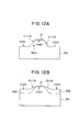
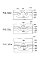
- FIG.1 shows the basic structure of a typical conventional laser diode of the so-called ridge type that produces an output optical beam in the visible wavelength region.
- the laser diode is constructed on the (100)-oriented upper major surface of a GaAs substrate 101 doped to the n-type.
- a buffer layer 102 of n-type GaAs is grown epitaxially on the (100)-oriented surface of the GaAs substrate 101, and an intermediate layer 103 of n-type InGaP is grown further on the buffer layer 102 epitaxially.
- a clad layer 104 of n-type InGaAIP is grown epitaxially, and an active layer 105 of undoped InGaP is grown epitaxially on the clad layer 104.
- the active layer 105 in turn is covered by a clad layer 106 of p-type InGaAIP, and an etching stopper layer 107 of p-type InGaP is grown on the clad layer 106.
- a clad layer 109 of p-type InGaAIP and an intermediate layer 110 of InGaP are grown consecutively to form a layered semiconductor body, and a silicon oxide layer (not shown) is deposited further on the layer 110.
- the silicon oxide layer is patterned in correspondence to the ridge structure to be formed to form a patterned silicon oxide mask, and the layered semiconductor body obtained previously is subjected to a wet etching process while using the patterned silicon oxide mask.
- a ridge structure including the layers 109 - 110 is formed on the etching stopper layer 107.
- a deposition of n-type GaAs is made such that the foregoing ridge structure is laterally supported by a pair of n-type GaAs regions formed as a result of the foregoing deposition of n-type GaAs.
- the layers 109 - 111 form a ridge structure supported laterally by the n-type GaAs regions 108a and 108b as already noted, and the ridge structure thus constructed forms a loss guide structure for guiding therethrough the optical beam produced in the active layer 105.
- the GaAs regions at both sides of the ridge structure absorbs the optical beam and changes the refractive index in response thereto.
- the band gap of GaAs is much smaller than the band gap of InGaP or InGaAIP.
- such a ridge structure, supported laterally by the p-type GaAs regions 108a and 108b, causes a confinement of the drive current within the ridge.
- the laser diode of FIG.1 is characterized by a low threshold current.
- InGaP for the material of the active layer 105, one can realize a laser oscillation at the wavelength of about 680 nm.
- the laser diode of FIG.1 is capable of producing output optical beam with a visible wavelength.
- the laser diode of FIG.1 has a problem in that there appears an astigmatism in the optical beam produced from the device. More specifically, there arises a discrepancy in the focal point of the optical beam that is emitted at the edge surface of the laser diode with a horizontal plane of beam divergence and the optical beam that is emitted at the same edge surface with a vertical plane of beam divergence.
- FIG.2 shows such a situation wherein two focal points, f 1 and f 2 , exist in the optical beam produced from the laser diode.
- the optical beam spreads in the vertical plane from the first focal point fi, while the optical beam spreads in the horizontal plane from the second focal point f 2 , wherein the focal point f 2 is offset from the focal point f 1 by several microns.
- the beam spot of the optical beam has an elongated elliptical shape that is not desirable for optical storage of information such as the optical disk systems as already described. It will be noted that the direction of elongation of the elliptical beam spot changes depending on the focusing state of the optical beam.
- the foregoing astigmatism occurring in the laser diode of FIG.1 is caused mainly by the difference in the degree of optical confinement between the vertical plane and the horizontal plane. As long as the loss guide structure that lacks the refractive structure for efficient lateral optical confinement is used, one cannot avoid the problem of astigmatism.
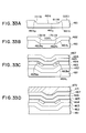
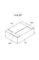
- FIG.3 shows the laser diode proposed previously by the present inventors.
- the laser diode is constructed on a GaAs substrate 201 doped for example to the p-type.
- the substrate 201 has a (100)-oriented upper major surface, and a mesa structure 201 a that is characterized by a (100)-oriented upper major surface and a pair of (111 )B-oriented side walls, is formed on the upper major surface as illustrated.
- the (100) surface of the mesa structure 201 a extends in the longitudinal direction of the laser diode and forms the basis of the stripe structure.
- a current confinement layer 202 of n-type GaAs is grown epitaxially while protecting the upper major surface of the mesa structure 201 a by a mask such as silicon oxide.
- a (311)B surface develops preferentially because of the slow rate of crystal growth in this crystal orientation.
- the epitaxial layer 202 thus grown is characterized by the well-developed (311)B surface that extends obliquely to the (100) surface of GaAs at both sides of the mesa structure 201a. Thereby, the (311)B surface forms another mesa structure that extends coincident to the stripe structure of the laser diode.
- a buffer layer 203 of p-type GaAs is grown epitaxially for providing an improved crystal surface for the subsequent epitaxial processes, and an intermediate layer 204 of p-type InGaP corresponding to the intermediate layer 110 is grown further on the buffer layer 203. Further, a clad layer 205 of p-type InGaAIP is grown epitaxially on the intermediate layer 204, and an active layer of undoped InGaP is grown epitaxially on the clad layer 205.
- a clad layer 207 of n-type InGaAIP is grown epitaxially, and an intermediate layer 208 of n-type InGaP corresponding to the intermediate layer 103 of FIG.1 is grown further thereon.
- a contact layer 208 of n -type GaAs is grown on the intermediate layer 110 epitaxially, and upper and lower electrode layers (not shown) are provided respectively on the upper major surface of the contact layer 209 and the lower major surface of the substrate 201.
- the epitaxial layers are grown by the MOCVD process for exact control of composition, and dopants are incorporated into the epitaxial layers as necessary during the epitaxial process.
- Zn is used for the p-type dopant, while Se or Si is used for the n-type dopant.
- Zn may be incorporated by admixing dimethylzinc ((CH 3 ) 2 Zn) to the source gas of the epitaxial layers, while Se is incorporated by admixing hydrogen selenide (H 2 Se).
- Si a gas of silane (SiH 4 ) or disilane Si 2 H e ) is used.
- a forward bias voltage is applied across the upper and lower electrodes to inject carriers into the active layer 206.
- holes are injected into the p-type substrate 201 and transported to the active layer 206 through the mesa structure 201 a due to the current confinement that is achieved by the n-type GaAs layer 202 at both sides of the mesa structure 201 a.
- the holes are injected preferentially at the central part of the clad layer 205 and transferred further to the active layer 206 for recombination with electrons that are injected from the upper electrode and transported to the active layer 206 via the layers 209 - 207.
- Such a recombination of electrons and holes initiates the well known stimulated emission process, and the stimulated emission process causes an amplification of the optical beam when reflectors are provided at both longitudinal ends of the laser diode for reflecting the optical beam back and forth through the laser diode.
- the stimulated emission process causes an amplification of the optical beam when reflectors are provided at both longitudinal ends of the laser diode for reflecting the optical beam back and forth through the laser diode.
- each layer 203 through 209 are all formed in conformity with the surface morphology of the second mesa structure in that each layer includes an elongated stripe region characterized by a (100) surface and extending in correspondence to the (100) surface of the mesa structure 201a.
- each stripe region is laterally defined by a pair of lateral regions located at both sides of the elongated (100) stripe surface and characterized by the (311)B surface in correspondence to the (311)B surface of the layer 202.
- the (100) surface is flat and extend parallel with the upper major surface of the mesa structure 201 a, while the (311)B surface extends obliquely to the (100) surface. Because of the lateral confinement of the optical beam in the stripe region of the active layer wherein the recombination of the carriers occurs predominantly, the problem of astigmatism is successfully eliminated in the device of FIG.3.
- each epitaxial layer includes crystallographically non-equivalent surfaces
- the nature or property of the epitaxial layers changes depending on the orientation of the crystal surface.
- the clad layer 205 is formed of three distinct regions characterized by respective, three crystallographically distinct surfaces, the first region characterized by the (100) surface and the second and third regions characterized by the (311)B surfaces, wherein the second and third regions are located at both sides of the first region and extend in the longitudinal direction of the laser diode together with the first region.
- concentration level of the dopant changes depending on the first through third regions of the clad layer 205. More specifically, the concentration level of Zn is higher in the second and third regions that is characterized by the (311)B surface as compared with the first region that is characterized by the (100) surface.
- the conventional laser diode of FIG.3 has a problem of large resistivity due to the relatively small Zn content in the epitaxial layer. More specifically, the small Zn content in the epitaxial layer causes the problem of small concentration of holes in the p-type layers, and the conventional laser diode has suffered from the problem of large resistivity and limited operational power. It should be noted that the laser diode would generate intolerable heat due to the large resistivity of the p-type layers, particularly when the injection current is increased. It is thought that this problem arises from the large vapor pressure of Zn that is in equilibrium with the crystal phase during the MOCVD process.
- Zn tends to concentrate more in the vapor phase than in the crystal as a result of the evaporation, and such a tendency is enhanced when the temperature of the epitaxial process is increased.
- the foregoing tendency contradicts with the requirement of large dopant concentration level in the epitaxial layers of the laser diode.
- Another and more specific object of the present invention is to provide a laser diode operational in the visible wavelength with a reduced astigmatism and with an improved current confinement.
- Another object of the present invention is to provide a process for fabricating a laser diode on a substrate that is formed with a stripe structure defined by crystallographically distinct surfaces and extending in a predetermined direction, wherein the device has a reduced resistivity associated with a high dopant concentration level in the clad layer.
- Another object of the present invention is to provide a simple process for forming an effective current confinement structure in a laser diode.
- Another object of the present invention is to provide a process for fabricating a laser diode, comprising the steps of: forming a first stripe structure defined by a plurality of crystallographically distinct surfaces each extending parallel with each other in a predetermined direction on an upper major surface of a semiconductor substrate; forming a layer of InGaAIP on said semiconductor substrate including said first stripe structure by a decomposition of organic source materials of In, Ga, AI and P while maintaining an epitaxial relationship with respect to said semiconductor substrate such that said layer of InGaAIP is formed with a second stripe structure corresponding to said first stripe structure, said layer of InGaAIP being formed such that said second stripe structure is formed of a plurality of crystallographically distinct surfaces corresponding to said plurality of crystallographically distinct surfaces that form said first stripe structure; and doping said InGaAIP layer to the p-type by incorporating Mg while growing said InGaAIP by admixing a gaseous source material of Mg into said source materials of
- the present invention one can obtain a relatively uniform distribution of Mg in the clad layer irrespective of the crystal surface on which the clad layer is grown.
- the uniform distribution of Mg is achieved even when the clad layer is formed on the stripe structure that includes crystallographically distinct surfaces, contrary to the conventional process wherein Zn is used for the dopant.
- the present invention is particularly useful for eliminating the spreading of the drive current in the stripe laser diodes wherein the GaAs substrate is formed with such a stripe structure.
- the use of Mg as the p-type dopant enables a high level doping that is advantageous for reducing the resistivity of the laser diode.
- the clad layer doped with Mg By growing the clad layer doped with Mg before an undoped active layer is grown, one can obtain a sharp boundary of conductivity type in correspondence to the interface between the clad layer and the active layer that is grown on the clad layer. By interrupting the supply of Mg, the incorporation of Mg into the clad layer is stopped immediately. On the other hand, when the Mg-doping is applied to the clad layer that is grown on the active layer formed already, there tends to appear a delay in the incorporation of Mg into the clad layer even when the supply of Mg is started, and the boundary of the conductivity type, which is essential for the double-hetero structure of the laser diode, may shift from the physical interface between the active layer and the clad layer.
- Another object of the present invention is to provide a process for fabricating a laser diode, comprising the steps of: forming a first stripe structure defined by a plurality of crystallographically distinct crystal surfaces including the (100) surface on an upper major surface of a semiconductor substrate, each of said crystal surfaces being formed to extend parallel with each other in a predetermined direction of said semiconductor substrate; forming a layer of InGaAIP on said semiconductor substrate including said first stripe structure by a decomposition of organic source materials of In, Ga, AI and P while maintaining an epitaxial relationship with respect to said semiconductor substrate such that said layer of InGaAIP is formed with a second stripe structure corresponding to said first stripe structure, said layer of InGaAIP being formed such that said second stripe structure is formed of a plurality of crystallographically distinct crystal surfaces corresponding to said plurality of crystal surfaces that form said first stripe structure; and doping said InGaAIP layer by incorporating a p-type dopant and an n-type dopant simultaneously while growing
- Mg or Zn as the p-type dopant
- Se as the n-type dopant
- the doping level of the p-type dopant and the n-type dopant appropriately.
- the morphology of the stripe structure characterized by the crystallographically distinct stripe surfaces is transferred to the clad layer, and the part of the active layer that is grown on the first stripe surface of the clad layer is supported laterally by a pair of sloped surfaces of the clad layer that are formed in correspondence to other stripe surfaces with an angle with respect to the first stripe surface.
- the optical radiation produced in the active layer is confined therein laterally by the first or second clad layer, and the problem of astigmatism is substantially eliminated.
- Another object of the present invention is to provide a process for fabricating a laser diode, comprising the steps of: forming a crystal surface on an upper major surface of a semiconductor substrate such that said crystal surface has a crystal orientation different from said upper major surface; and forming a clad layer on said substrate while maintaining an epitaxial relationship between said clad layer and said substrate; wherein said step of forming the clad layer comprises a step of incorporating a p-type dopant and an n-type dopant simultaneously.
- one can obtain a clad layer wherein the conductivity type is changed selectively therein by a single deposition step. Thereby, one can fabricate a laser diode having an excellent confinement of current easily.
- Another object of the present invention is to provide a stripe laser diode, comprising: a substrate of a semiconductor material having an upper major surface and a lower major surface and extending in a longitudinal direction from a first end to a second, opposite end; a stripe structure formed on said upper major surface of said substrate as a part of said substrate, said stripe structure comprising a first stripe surface formed of the (100) surface and extending in said longitudinal direction and a pair of different stripe surfaces each having a crystal orientation different from the (100) surface and extending in said longitudinal direction at both lateral sides of said first stripe surface; a first clad layer of InGaAIP doped provided on said substrate to extend in said longitudinal direction from a first end to a second, opposite end, said first clad layer having upper and lower major surfaces and including a stripe structure formed therein in conformity with said stripe structure of said substrate; an active layer of undoped semiconductor material having a band gap smaller than said first clad layer and provided on said first clad layer to
- Mg can be doped into the clad layer with increased concentration level as compared with Zn, one can increase the conductivity of the laser diode with respect to the drive current.
- the stripe structure of the active layer is laterally sandwiched by the first or second clad layer in the stripe laser diode, one can minimize the problem of astigmatism.
- Another object of the present invention is to provide stripe laser diode, comprising: a semiconductor substrate doped to a first conductivity type, said substrate having an upper major surface and a lower major surface and extending in a longitudinal direction of the laser diode from a first end to a second, opposite end; a first stripe structure formed on said upper major surface of said semiconductor substrate as a part of said substrate, said first stripe structure comprising a first stripe surface formed of the (100) surface and extending in said longitudinal direction and a pair of side surfaces each formed of a crystal surface different from the (100) surface and extending in said longitudinal direction at both lateral sides of said first stripe surface; a first clad layer of InGaAIP having upper and lower major surfaces and provided on said semiconductor substrate to extend in said longitudinal direction from a first end to a second, opposite end; a second stripe structure formed on said upper major surface of said first clad layer to extend in said longitudinal direction as a part of said first clad layer and in conformity with said first stripe structure
- concentration level of the p-type dopant and the n-type dopant such that the carrier concentration level increases at said first stripe region or such that the conductivity type changes at said first stripe region.
- the property or nature of the semiconductor material changes depending on the crystal surface or orientation. This applies not only to the physical property of the crystal known as anisotropy but also to the crystal growth conducted by the epitaxial processes.
- the composition of the semiconductor material tends to change depending on the crystal surface. For example, it is reported that the content of Zn incorporated into the InGaAIP crystal grown by the MOCVD process increases with increasing offset angle of the crystal surface on which the epitaxial growth occurs, with respect to the (100) surface.
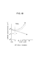
- FIG.4 shows the concentration level of Zn and Mg that are added to an epitaxial layer of InGaAIP as a dopant for various crystal surfaces, wherein the data for Zn and Mg is discovered for the first time by the inventors of the present invention (Kondo, M., Anayama, C., Tanahashi, T. and Yamazaki S., Sixth International Conference on Metalorganic Vapor Phase Epitaxy, IEEE Catalog #92TH0459-8, June 8 - 11, 1992). In FIG.4, the data for Zn by other references are also illustrated.
- doping of Mg or Zn is achieved while growing the InGaAIP layer by the MOCVD process, by admixing a gaseous source such as dimethylzinc ((CH 3 ) 2 Zn) or bis(cyclo-penta-dienyl)magnesium ((CsHs) 2 Mg) to the source gas of Al, In, Ga and P.
- a gaseous source such as dimethylzinc ((CH 3 ) 2 Zn) or bis(cyclo-penta-dienyl)magnesium ((CsHs) 2 Mg)
- the solid and open circles as well as the solid and open squares represent the data that is obtained by the experiment by the inventors of the present invention, wherein the open circles and open squares represent the result of the SIMS analysis, while the solid circles and solid squares represent the result of the C-V measurement.
- TABLE I The condition of the MOCVD process is summarized in TABLE I below.
- the Zn content increases steeply with increasing tilt angle of the crystal surface toward the (111)A surface (designated as A direction in FIG.4) from the (100) reference surface and then decreases with a further increase of the offset angle, wherein the peak of the Zn concentration appears generally in coincidence to the (311)A surface.
- the (311) surface that is offset or tilted toward the (111)A surface exposes the Ga surface and hence forms the (111)A surface.
- the (311) surface tilted toward the (311)B surface exposes the As surface and forms the (311)B surface.
- the Mg concentration level remains substantially constant even when the crystal surface is tilted toward the (311)B surface.
- the content of Mg is substantially the same in the (100) surface and the (311)B surface.
- the Mg content increases with increasing tilt angle of the crystal surface.
- the Mg content is much larger than the Zn content in any of the crystal surfaces.
- FIG.5 shows the content of Se incorporated into the InGaAIP layer for various crystal surfaces.
- the growth of the InGaAIP layer is achieved by the MOCVD process with the condition identical with the condition of TABLE I.
- the Se content increases slightly in the (311)B surface as compared with the (100) surface and increases steeply when the offset angle exceeds the angle corresponding to the (311)B surface.
- the Se content decreases steeply with increasing offset angle from the (100) surface.
- FIG.6 shows the effect of Mg doping on the (100) surface of the InGaAIP crystal.
- the hole concentration level of about 4 X 10 17 cm -3 by setting the mole ratio of the (CsHs)- 2 Mg gas with respect to the source gases of the group III elements, to about 3 X 10- 4.
- the mole ratio may be set to 1 X 10 -3 cm -3 .
- Mg occupies the site of the group III elements in the crystal of InGaAIP and acts as the p-type dopant that releases a hole.
- FIG.7 is a diagram similar to FIG.6 and shows the effect of Zn doping on the various crystal surfaces of InGaAIP.
- the Zn content increases with increasing mole ratio of the Zn source gas and changes depending on the crystal surfaces.
- the concentration level of the holes is much smaller than that of Mg shown in FIG.6 in conformity with the result of FIG.4.
- the oblique part of the layer 205 that is grown on the (311)B surface is doped with a larger concentration level of Zn as compared with the flat part grown on the (100) surface as illustrated in FIG.8.
- the carrier density decreases in correspondence to the (100) part that forms the stripe structure
- the resistivity of the clad layer 205 increases in correspondence to the stripe part on which the essential part of the active layer is formed.
- the current injected at the bottom electrode inevitably circumvents the stripe part of the active layer 206 wherein the recombination of carriers should occur, and the efficiency of the laser oscillation is deteriorated inevitably.
- FIG.4 indicates further that the problem of unwanted increase of the resistivity of the InGaAIP layer in correspondence to the (100) surface can be eliminated when the Mg doping is applied in place of the Zn doping.
- FIG.9 shows the Mg concentration level as well as the corresponding hole concentration level together with the resistivity distribution realized in the InGaAIP layer that is grown on the mesa structure having the (100) surface and a pair of (311)B surfaces at both sides of the (100) surface.
- the Mg content and hence the hole concentration level remains substantially constant throughout the InGaAIP layer irrespective of the crystal surfaces.
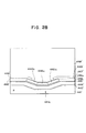
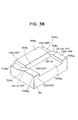
- the laser diode is constructed on a p-type GaAs substrate 301 that may be doped by Zn to have a carrier concentration level of 1 X 10 19 cm -3 .
- the GaAs substrate 301 has an upper major surface and a lower major surface each having the (100) orientation, and a mesa structure 301 a is formed on the upper major surface to extend in the longitudinal direction of the laser diode that is set coincident to the (011) direction of the substrate 301.
- the mesa structure is defined laterally by sloped surfaces 301 b i and 301 b 2 each having the (111)B orientation, and there extends a stripe surface 301 having the (100) orientation in coincidence to the longitudinal direction of the laser diode.
- a current confinement layer 302 of n-type GaAs is grown epitaxially with a thickness of about 1 ⁇ m such that the stripe surface 301 extends in the longitudinal direction of the laser diode.
- the current confinement layer 302 is doped by Si or Se to a carrier concentration level of about 5 X 10 18 cm -3 and forms a pair of well developed oblique surfaces 303bi and 303b 2 at both sides of the exposed stripe surface 301 c of the GaAs substrate.
- the oblique surfaces 303bi and 303b 2 are equivalent with each other and forms a (311)B surface.
- a second mesa structure above the first mesa structure with an (100) oriented stripe surface formed coincident to the (100) oriented stripe surface 301 c, and a pair of oblique or sloped surfaces 303bi and 303b 2 each having the (311)B orientation are formed to extend at both sides of the stripe surface 301 c in the longitudinal direction of the device.
- the substrate 301 and the current confinement layer 302 forms a substrate structure 300, and the essential part of the laser diode is constructed on the substrate structure 300 by an MOCVD process.
- TMI trimethylindium
- TMG trimethylgallium
- AI is supplied in the form of triethylaluminum (TEA)
- As is supplied in the form of arsine
- P is supplied in the form of phosphine, as commonly practiced in the art, with a condition similar to the condition given in TABLE I.
- a buffer layer 303 of GaAs doped to the p-type by Zn and/or Mg with the carrier concentration level of 1 X 10 18 cm -3 is grown epitaxially by a MOCVD process with a thickness of about 0.1 - 0.2 ⁇ m, and a first intermediate layer 304 of InGaP, doped to the p-type by Zn and/or Mg with the carrier concentration level of 1 X 10 18 cm -3 , is grown on the buffer layer 303 epitaxially with a thickness of about 0.1 ⁇ m also by a MOCVD process.
- the morphology of the second mesa structure of the substrate structure 300 is transferred to the epitaxial layers 303 and 304, and the InGaP layer 304 thus grown has a corresponding mesa structure of the upper major surface such that there is formed a (100) oriented stripe surface and a pair of (311)B oriented sloped surfaces extending in the longitudinal direction of the device or the (011) direction at both sides of the (100) oriented stripe surface.
- the intermediate layer 304 acts similar to the intermediate layers 110 and 204 and reduces the kink or spike appearing in the valence band for facilitating the transport of the carriers.
- a first clad layer 305 of p-type InGaAIP that forms the essential part of the present embodiment and having a composition of (Al o . 7 Ga o . 3 ) o . s ln o . s , is grown epitaxially by a MOCVD process with a thickness of about 1 ⁇ m.
- the doping of the first clad layer 305 is achieved by incorporating bis(cyclo-pentadienyl)magnesium into the source gases of TMI, TEG, TMA and phosphine, with a flowrate determined based upon the relationship of FIG.6 such that a carrier concentration level of 1 X 10 18 cm -3 is achieved.
- the mesa morphology of the substrate structure 300 is transferred further to the upper major surface of the first clad layer 305.
- the upper major surface of the clad layer 305 includes the stripe-like (100) surface corresponding to the apex of the mesa and two (311)B surfaces extending obliquely at both sides of the (100) stripe surface.
- an active layer of undoped InGaP is grown with a thickness of 0.07 /1 .m.
- the mesa morphology on the upper major surface of the clad layer 305 is transferred to the upper major surface of the active layer 306.
- the active layer 306 includes an (100) stripe surface and two oblique surfaces having the (311)B orientation in correspondence to the mesa structure.
- a second clad layer 307 of InGaAIP doped to the n-type is grown epitaxially by an MOCVD process with a thickness of about 1 ⁇ m.
- the doping to the n-type is achieved by incorporating hydrogen selenide or silane such as monosilane or disilane into the source gases of In, Ga, AI and P with the condition similar to the condition of TABLE I.
- hydrogen selenide or silane such as monosilane or disilane
- the active layer 306 is laterally bounded by the sloped surfaces of the clad layer 307.
- a second intermediate layer 308 of n-type InGaP, doped by Se or Si to the carrier concentration level of about 1 X 10 18 cm- 3 is grown epitaxially with a thickness of about 0.1 ⁇ m, and a contact layer of n-type GaAs, doped to the carrier concentration level of 3 X 1018 cm-3 is grown with a thickness of about 1 /1.m.
- the second intermediate layer 308 also reduces the spike in the conduction band, similarly to the first intermediate layer 304.
- an upper electrode 310 and a lower electrode 311 are deposited respectively on the upper major surface of the contact layer 309 and the lower major surface of the substrate 301 in ohmic contact therewith. Further, it will be noted that the edge surfaces opposing with each other at the longitudinal ends form the reflectors of the laser diode as usual.
- Mg doping to the second clad layer 307 instead of doping the same to the n-type by Se or Si.
- FIG.11 (A) shows the sequence of doping for incorporating Mg into the clad layer 307 by the MOCVD process in the device that is constructed on the n-type GaAs substrate.
- the deposition of the clad layer 307 is started after the active layer 306 of undoped InGaP is grown, wherein it will be noted that the incorporation of Mg into the clad layer 307 occurs after a substantial time elapsed from the commencement of growth of the clad layer 307. This in turn means that the part of the clad layer 307 that contacts with the active layer remains in the undoped state, unless additional doping process is employed simultaneously. When the clad layer 307 is undoped, it will be easily understood that the injection of the carriers to the active layer 306 does not occur.
- the process of FIG.11 (A) employs a doping of Zn in order to compensate for the depletion of Mg in the foregoing part of the clad layer 307.
- Zn is supplied for example in the form of dimethylzinc together with the gaseous source materials for Al, Ga, In and P.
- the incorporation of Zn occurs immediately and the p-type conductivity is guaranteed for the clad layer 307.
- the supply of Zn is interrupted and Mg starts to be incorporated into the clad layer 307 with a substantial concentration level.
- the growth of the GaAs buffer layer 303 is achieved on the p-type substrate structure 300 with the doping to the p-type by incorporating Zn into the layer 303.
- the supply of Mg is started by admixing bis(cyclo-penta-dienyl)magnesium into the source gases of the GaAs layer 303.
- the content of Mg increases with the growth of the GaAs buffer layer 303 and becomes stationary when the growth of the first intermediate layer 304 is started on the buffer layer 303.
- the supply of Zn is interrupted.
- the incorporation of Zn into the layer 303 stops immediately when the supply of Zn is terminated.
- the growth of the intermediate layer 304 is completed, the growth of the first clad layer 305 is started while continuing the supply of Mg.
- the concentration level of the holes in the layers 304 and 305 remains substantially constant.
- the clad layer 305 is grown to the predetermined thickness, the supply of Mg is interrupted, and the composition of the source material for the epitaxial layer is changed simultaneously. Thereby, the growth of undoped active layer 306 is started.
- the second clad layer 307 of Se- or Si-doped InGaAIP is grown as usual.
- FIG.11 (B) it will be noted that one can obtain a sharp boundary of conductivity type in correspondence to the physical boundary between the first clad layer 305 and the active layer 306 that is grown thereon, without employing additional doping process by Zn to the layer 305.
- the process of FIG.11 (B) corresponding to the structure described with reference to FIG.10 is more preferable to the process of FIG.11 (A) wherein the conductivity type of the substrate as well as the epitaxial layers is reversed, although this does not deny the usefulness of the process of FIG.11 (A).
- FIG.10 Next, the fabrication process of the structure of FIG.10 will be described with reference to FIGS.12(A) - 12(D).
- a silicon oxide layer is provided on the (100) upper major surface of the p-type GaAs substrate 301 and patterned subsequently to form a silicon oxide stripe 21 such that the silicon oxide stripe 21 extends in the (011) direction. Further, while protecting the upper major surface of the substrate 301 by the silicon oxide stripe 21 thus formed, the substrate 301 is subjected to an wet etching process conducted in a mixture of H 2 S0 4 , H 2 0 2 and H 2 0 to form a mesa structure that corresponds to the mesa structure 301 a and includes a (100) stripe surface extending in the (011) direction at the top thereof with a width of about 5 ⁇ m.
- the mesa structure 301 a is laterally bounded by a pair of oblique surfaces both characterized by the (111)B surface.
- the (100) upper major surface of the GaAs substrate 301 extends parallel to the (100) stripe surface of the mesa structure 301 a.
- the deposition of the n-type GaAs layer 302 is achieved by the MOCVD process while protecting the (100) stripe surface of the mesa structure 301 a by the mask 21.
- the mask 21 is made of silicon oxide, the growth of the epitaxial layer does not occur on the mask 21, while the layer 302 grows on the (100) upper major surface of the GaAs substrate 301 extending at both sides of the mesa structure 301 a.
- oblique layers 303b i and 303b 2 characterized by the (311)B crystal surface develops on the upper major surface of the layer 302 at both sides of the (100) stripe region as shown in FIG.12(B) in correspondence to the (111)B surface of the mesa structure 301 a.
- the (311)B surfaces 303bi and 303b 2 form a second mesa structure together with the (100) stripe surface.
- the epitaxial growth of the layers 303 through 309 is achieved by the MOCVD process consecutively on the structure of FIG.12(B) as already described, wherein the growth of the layers 304 and 305 is achieved by the process described already with reference to FIG.11 (B). Thereby, one obtains a layered semiconductor body shown in FIG.12(C).
- upper and lower electrodes 310 and 311 are deposited respectively on the upper major surface of the contact layer 309 and on the lower major surface of the substrate 301. Thereby, the layered structure of the laser diode formed as shown in FIG.12(D).
- the construction for confining the injection current according to the first embodiment is effective also when the conductivity type of the epitaxial layers is reversed. More specifically, when one uses the n-type GaAs substrate in place of the p-type substrate 301, the conductivity type is reversed in each of the epitaxial layers. There, the process of FIG.11 (A) is applied to the growth of the p-type clad layer 307 rather than the n-type clad layer 305.
- FIGS.13(A) and 13(B) show the principle of the second embodiment.
- the concentration level of Se increases slightly in the (311)B surface as compared with the (100) surface.
- the concentration level of Se and hence the electron density decrease slightly in the InGaAIP layer in correspondence to the (100) surface as compared with the (311)B surface that forms the mesa structure together with the (100) surface.
- the concentration level of Mg and hence the hole density remains substantially constant in the same InGaAIP crystal irrespective of the crystal surfaces.
- the concentration level of Mg is larger than the concentration level of Se, doped simultaneously to Mg, in any of the (311)B surface and (100) surface, such that the InGaAIP crystal is doped to the p-type irrespective of the crystal surface, while it should be noted that there appears a difference in the resistivity depending on the crystal surface because of the different carrier concentration level in the (311)B surface and in the (100) surface. More specifically, the hole density increases in correspondence to the (100) surface as compared with the (311)B surface because of the reduced electron density in the (100) surface. Using the principle of FIG.13(A), one can decrease the resistivity of the clad layer selectively in correspondence to the (100) stripe region while increasing the resistivity in correspondence to the (311)B side walls of the mesa structure.
- FIG.13(B) shows another principle of the second embodiment device wherein the concentration level of simultaneously doped Mg and Se is adjusted such that the conductivity type of InGaAIP changes depending on the crystal surface.
- concentration level of simultaneously doped Mg and Se is adjusted such that the conductivity type of InGaAIP changes depending on the crystal surface.
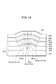
- FIG.14 shows the transversal cross section of the laser diode of the second embodiment wherein the foregoing principle is applied for realizing a current confinement structure.
- the device has essentially the same structure as the device of FIG.10, only the essential part of the device will be described.
- the first clad layer 305 is formed by the epitaxial process with the simultaneous doping of Mg and Se such that Mg has a concentration larger than Se for both the (311)B surface and the (100) surface as explained with reference to FIG.13(A).
- Mg has a concentration larger than Se for both the (311)B surface and the (100) surface as explained with reference to FIG.13(A).
- concentration level of Mg and Se in the respective parts of the InGaAIP clad layer 305 as shown in TABLE II below.
- the resistivity of the clad layer 305 increases in correspondence to the part grown on the (311)B surface as indicated in FIG.14 by the hatching, and the drive current, supplied at the electrode 311 and confined laterally by the n-type GaAs layer 302, is selectively injected to the stripe part of the active layer 306 through the low-resistivity (100) region of the clad layer 305 located immediately above the (100) stripe surface of the mesa structure.
- the drive current supplied at the electrode 311 and confined laterally by the n-type GaAs layer 302
- the doping level of Mg and Se may be set as shown in the following TABLE III.
- the current confinement structure is formed within the clad layer that is formed immediately adjacent to the active layer.
- the divergence of the drive current after the current confinement is minimized.
- the device of FIG.14 is improved further over the device of FIG.10 with respect to the lateral current confinement.
- FIGS.15(A) and 15(B) show the principle of construction of such a current confinement structure, wherein FIG.15(A) shows the case in which the InGaAIP layer 307 is doped to the n-type irrespective of whether the layer 307 is grown on the (100) surface or (311)B surface, while FIG.15(B) shows the case where the conductivity type changes in the layer 307 depending on the crystal surface.
- the resistivity changes, although the conductivity type does not change, such that the electron density decreases at the part grown on the (311)B surface as compared with the part that is grown on the (100) surface.
- the drive current flows selectively through the mesa region grown on the (100) stripe surface as shown in FIG.14, and the degree of current confinement is even more improved as compared with the embodiment wherein the current confinement structure is provided only in the first clad layer 305.
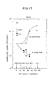
- FIG.16 shows the concentration level of Zn incorporated in a GaAs layer grown by a MOCVD process for various crystal surfaces on which the GaAs layer is grown
- FIG.17 shows the concentration level of Se that is incorporated in the GaAs layer for various crystal surfaces.
- the Zn content increases with increasing offset angle to the (111)A surface and shows a maximum generally in correspondence to the (311)A surface, while the Se content decreases monotonously with increasing offset angle to the (111)A surface.
- FIG.18 shows the change of the conductivity type that can be achieved in a GaAs layer grown by the MOCVD process.
- a high resistivity layer when the GaAs layer is grown on the (100) surface and doped simultaneously by Se and Zn with the equal concentration level of about 1 X 10 18 CM - 3.
- the Zn content decreases gradually and the GaAs layer shows the n-type conductivity.
- the concentration level of Se is set slightly smaller than Zn
- the GaAs layer grown on the (100) surface shows the p-type conductivity due to the excess in the holes produced by Zn.
- the Zn content decreases gradually and the conductivity type reverses in correspondence to the offset angle of about 10 degrees as can be seen in FIG.18.
- FIG.19 shows the structure of the laser diode of the third embodiment, wherein a GaAs current confinement layer is provided within the clad layer.
- the laser diode has a structure similar to the device of FIG.10 or FIG.14 except for one point that the intermediate layers 304 and 308 are omitted.
- those parts that correspond to the parts described in the previous embodiments will be designated by the same reference numerals and the description will be omitted.
- a thin GaAs layer 312 is provided within the clad layer 305 such that the clad layer 305 is split into a lower part 305a and an upper part 305b.
- the GaAs layer has a thickness of about 8 nm and is divided into three distinct regions, a first, stripe-like region 312a formed on the (100) surface and extending in correspondence to the mesa structure, a pair of second regions 312b, and 312b 2 formed on the (311)B surface in correspondence to the mesa structure and extending at both sides of the region 312a.
- the GaAs layer 312 is grown by the MOCVD process and doped simultaneously by Zn and Se such the region 312a is doped to the p-type while the regions 312b, and 312b 2 are doped to the n-type.
- a doping of the layer 312 can be achieved by setting the concentration level of Zn and Se as shown in FIG.18. More specifically, one may admix dimethylzinc and hydrogen selenide into the source gases of TEG and arsine for growing the GaAs layer 312 with respective concentration levels such that a Zn concentration level of about 1 X 10 18 cm- 3 and a Se concentration level of about 5 X 10 17 cm- 3 are achieved in the (100) surface.
- the n-type regions 312b i and 312b 2 are doped to the n-type and act to block the current injected to the active layer 306, and the effect of the current confinement is enhanced substantially.
- FIG.20 shows a modification of the third embodiment.
- the device has a structure similar to the device of FIG.19 except for the point that the conductivity type of each epitaxial layers as well as the conductivity type of the GaAs substrate is reversed. More specifically, the device is constructed on an n-type GaAs substrate 321 that has a mesa structure 321 a corresponding to the mesa structure 301 a of the substrate 301. On the substrate 321, epitaxial layers 322 through 329 are grown in correspondence to the epitaxial layers 302 - 309 of FIG.19 except for the conductivity type.
- the construction of the device of FIG.20 is obvious from the construction of the device of FIG.19, further description about the details will be omitted.
- a thin GaAs layer 331 having a thickness of about 8 nm is provided within the p-type clad layer 327 of InGaAIP such that the clad layer 327 is divided into a first layer 327a located below the layer 331 and a second layer 327b located above the layer 331.
- the layer 331 is doped simultaneously by Zn and Se such that the layer 327 is divided into a p-type region 331 a formed in correspondence to the (100) stripe surface of the mesa structure and two n-type regions 331b, and 331 b 2 formed at both sides of the n-type region 327a in correspondence to the (311)B surface.
- the doping of the GaAs layer 331 can be achieved similarly to the layer 312 and the description will be omitted.
- FIG.21 shows another modification of the third embodiment, wherein the device is constructed on a p-type GaAs substrate 341 covered by an n-type GaAs current blocking layer 342 that corresponds to the layer 302, wherein there is provided a groove 341 a on the upper major surface of the layer 342 such that the groove penetrates through the layer 342 and reaches the substrate 341.
- the groove 341 a forms a negative mesa structure characterized by a (100) oriented stripe-like bottom surface 341 formed of an exposed surface of the GaAs substrate 341 and a pair of (111)B surfaces 341 bi and 341 b 2 at the both sides of the (100) stripe-like bottom surface.
- the (100) stripe surface has a width of 5 ⁇ m similarly to the previous embodiments.
- a p-type GaAs layer is grown epitaxially while protecting the upper major surface of the n-type GaAs layer 342, except for the mesa structure 341 a, by a silicon oxide mask 52. See FIG.22(A).
- a p-type region 343 is grown selectively in correspondence to the exposed surface of the negative mesa structure 341 a such that the p-type region 343 forms a second negative mesa structure 341 a corresponding to the first mesa structure 341 a and is characterized by a (100) stripe surface 343a at the bottom and a pair of (311)B surfaces 343b i and 343b 2 at both sides of the stripe surface 343a.
- the p-type GaAs substrate 341, the n-type GaAs layer 342 and the p-type GaAs layer 343 form a substrate structure 340 on which the essential part of the laser diode is constructed.
- a buffer layer 344 of p-type GaAs is grown epitaxially with a thickness of about 0.2 /1 .m and in conformity with the morphology of the second mesa structure, and a first clad layer 345 of p-type InGaAIP is grown on the buffer layer 344 in conformity with the morphology of the second mesa structure.
- the clad layer 345 may be doped by incorporating Mg as described in the first embodiment or by incorporating Mg and Se simultaneously as described in the second embodiment.
- a current blocking layer 346 of p-type GaAs is grown epitaxially with the doping achieved simultaneously by Zn and Se, such that the layer 346 has the p-type in correspondence to the region that is grown on the (100) surface and such that the layer 346 has the n-type in correspondence to the region that is grown on the (311)B surface.
- a second clad layer 347 of p-type InGaAIP is grown on the current blocking layer 346 thus grown, and an active layer 348 of undoped InGaP is grown on the clad layer 347 thus formed.
- an n-type clad layer 349 is grown on the active layer 348 and a contact layer 350 of n-type GaAs is grown on the clad layer 349 as indicated in FIG.22(B).
- a contact layer 350 of n-type GaAs is grown on the clad layer 349 as indicated in FIG.22(B).
- the foregoing process for growing the epitaxial layers is achieved by the known MOCVD process.
- an upper electrode 351 and a lower electrode 352 are provided respectively on the upper major surface of the contact layer 350 and the lower major surface of the substrate 341, and the structure shown in FIG.21 is obtained.
- the concentration level of Mg and Se in the p-type InGaAIP clad layers 345 and 347 such that the clad layers have the p-type conductivity in correspondence to the region grown on the (100) strip surface of the mesa structure and the n-type conductivity in correspondence to the region grown on the (311)B surface.
- the diagram shows the carrier concentration level in an InGaAIP layer grown on various crystal surfaces and doped by Zn or Se, wherein the solid circles represent the change of the concentration level of electrons released from Se as a function of the increasing tilt angle toward the (111)A surface, while the open circles represent the change of the concentration level of the holes released from Zn. Further, the solid and open triangles represent respectively the change of the electron concentration level and the hole concentration level for the case wherein the InGaAIP layer is doped simultaneously by Zn and Se.
- the electrons released from Se are predominant over holes that are released from Zn for the layer that is grown on the (100) surface, while this relationship is reversed in the epitaxial layer grown on the (311)A surface, in conformity with the relationship of FIGS.4 and 5. More specifically, the layer grown on the (311)A surface is doped to the p-type in contrast to the layer grown on the (100) surface that is doped to the n-type under the same doping condition.
- an electron concentration level of about 1 X 1018 cm-3 and a hole concentration level of about 2 X 1016 cm-3 are achieved on the (100) surface, while an electron concentration level of about 6 X 10 6 cm -3 and an electron concentration level of about 1 X 10 18 cm -3 is achieved on (311)A surface in the same condition.
- the relationship of FIG.23 is effective for controlling the conductivity type of the InGaAIP layer based upon the orientation on the crystal surface on which the layer is grown.
- the principle of FIG.23 can be applied to the various embodiments described heretofore, by merely setting the direction of elongation of the (100) stripe surface in the (011) direction such that the (311)A surface is exposed at the side surface of the mesa structure in place of the (311)A surface.
- the magnitude of change of the carrier concentration level is larger in the (311)A surface than in the (311)B surface, a more effective current confinement can be achieved by using the (311)A surface.
- the embodiments described heretofore take the advantage of the above mentioned feature of large magnitude of change of the carrier concentration level.
- FIG.24(A) shows the change of the electron concentration level and the resistivity corresponding to a first setting of the concentration level of Zn and Se, wherein the concentration levels of Zn and Se are set such that there occurs no change of the conductivity type between the part grown on the (100) surface and the part grown on the (311)A surface.
- the carrier concentration level and hence the resistivity increases substantially in correspondence to the part of the epitaxial layer grown on the (100) surface and one can achieve an effective concentration of current when the doping scheme of FIG.24(A) is applied for the fabrication of the clad structure of the laser diode.
- FIG.24(B) shows, on the other hand, a second scheme of doping wherein the concentration levels of Zn and Se are set such that there occurs a reversal of the conductivity type depending on the part of the InGaAIP layer grown on the (100) surface and the part grown on the (311)A surface. There, the Se concentration level exceeds the Zn concentration level in the part of the InGaAIP layer grown on the (100) surface, while the relationship reverses in the part that is grown on the (311)A surface.
- the laser diode of the present embodiment is constructed on a p-type GaAs substrate structure 401.
- the substrate structure 401 is formed with a mesa structure 401 a corresponding to the mesa structure 301 a such that the mesa structure 401 a is defined by a (100) oriented stripe surface 401 c extending in the (01 T) direction and laterally bounded by a pair of side surfaces 401b, and 401 b 2 both having the (311)A orientation, and a buffer layer 402 of p-type GaAs is grown on the substrate structure 400 in correspondence to the buffer layer 301.
- an intermediate layer 403 corresponding to the intermediate layer 304 is grown on the buffer layer 402.
- a clad layer 404 corresponding to the clad layer 305 is grown with a doping achieved by Mg such that the clad layer 404 is doped to the p-type uniformly.
- an undoped active layer 405 is grown epitaxially as in the previous embodiments, and a first clad layer 406 of n-type InGaAIP is grown further on the active layer 405 with a doping achieved by Se such that the layer 406 is doped to the n-type uniformly for the entirety of the layer 406.
- another clad layer 407 of n-type InGaAIP is grown on the clad layer 406 epitaxially such that the clad layer 407 incorporates Zn and Se simultaneously while it is grown on the clad layer 406 by the MOCVD process.
- the concentration level of Zn and Se is set as shown in FIG.24(A) or FIG.24(B) such that the clad layer 407 shows an increased resistivity in correspondence to the part that is grown on the (311)A surface and designated in FIG.25 as 407bi and 407b 2 , or such that the clad layer 407 shows a p-type conductivity in correspondence to the foregoing regions 407bi and 407b 2 .
- an n-type intermediate layer 408 of InGaP is grown in correspondence to the intermediate layer 308 of the previous embodiments, and a current blocking layer 409 of p-type GaAs is grown further on the intermediate layer 408.
- the layer 409 is patterned such that the intermediate layer 408 is exposed in correspondence to the mesa structure, and a contact layer 410 of n-type GaAs is grown on the current blocking layer 409 in contact with the exposed upper major surface of the intermediate layer 408.
- an upper electrode 411 and a lower electrode 412 are deposited respectively in ohmic contact with the upper major surface of the layer 410 and with the lower major surface of the substrate 401.
- FIG.26 is a diagram showing a modification of the fourth embodiment that uses an n-type substrate 421 in place of the p-type substrate 401.
- the substrate 421 includes a mesa structure 421 a defined by the (100) oriented stripe-like surface 421 c laterally defined by a pair of (111)A oriented surfaces 421 b 1 and 421 b 2 , wherein a p-type GaAs layer 422 is grown on the substrate 421 similarly to the layer 322 of FIG.20.
- the p-type GaAs layer 422 has a second mesa structure similar to the layer 322 such that the second mesa structure is characterized by the (100) oriented stripe-like top surface and a pair of (311)A oriented side surfaces 423b i and 423b 2 , and a buffer layer 423 of n-type GaAs is grown on the layer 422. Further, an intermediate layer 424 of n-type InGaAIP is grown on the buffer layer 423, and a first clad layer 425, of n-type InGaAIP is grown on the intermediate layer 424.
- the layer 425 is doped simultaneously by Zn and Se such that the layer 425 is divided into a first region 425a grown on the (100) surface of the mesa structure 421 a and a pair of second regions 425bi and 425b 2 formed at both sides of the first region 425a in correspondence to the (311)A oriented surfaces of the second mesa structure, similarly to the previous embodiments.
- another clad layer 425b 2 of n-type InGaAIP is grown on the layer 425b 1 with the doping by Se, and an active layer 426 of undoped InGaP is grown on the layer 425 2 epitaxially and in conformity with the morphology of the mesa structure.
- an active layer 426 of undoped InGaP is grown on the layer 425 2 epitaxially and in conformity with the morphology of the mesa structure.
- a clad layer 427 of p-type InGaAIP is grown epitaxially, and an intermediate layer 428 of p-type InGaP is grown further on the clad layer 427.
- a contact layer 429 of p-type GaAs is grown on the layer 428 as usual.
- an upper electrode 430 is provided on the upper major surface of the p-type GaAs contact layer 429 and a lower electrode 431 is provided on the lower major surface of the n-type GaAs substrate 421.
- FIG.27 shows another modification of the fourth embodiment, wherein the device is constructed on an n-type GaAs substrate 441 that is covered by a current confinement layer 442 of p-type GaAs.
- the layer 442 as well as the substrate 441 are formed with a negative mesa structure 441 a similar to the mesa structure 341 a of FIG.21, and an intermediate layer 443 of n-type InGaP is grown on the layer 442 to cover the mesa structure 441 a.
- a first clad layer 444, of n-type InGaAIP is grown epitaxially, wherein the layer 444, is doped simultaneously by Zn and Se with the concentration level set as indicated in FIG.24(A) or FIG.24(B).
- the clad layer 444 is divided into a low resistivity n-type region 444a corresponding to the (100) stripe surface and a pair of high resistivity n-type regions 444b i and 444b 2 respectively grown on the (311)A surface of the mesa structure.
- the clad layer 444 achieves an efficient current confinement.
- the region 444a is doped to the n-type while the regions 444b i and 444b 2 are doped to the p-type.
- the regions 444b i and 444b 2 block the injection current, and the construction of the latter is useful also for achieving an efficient current confinement.
- another clad layer 444 2 of n-type InGaAIP is grown epitaxially, and an active layer 445 of undoped InGaP is grown on the layer 444 2 Further, a clad layer 446 of p-type InGaAIP is grown on the upper major surface of the active layer 445, and an intermediate layer 447 of p-type InGaP is grown on the layer 446. On the layer 446, a p-type contact layer 448 is grown as illustrated. Further, an electrode 451 and an electrode 452 are provided respectively on the upper major surface of the clad layer 448 and on the lower major surface of the substrate 441.
- FIG.28 shows another modification of the fourth embodiment, wherein the device of FIG.28 is constructed on a p-type substrate structure 441' that has a construction similar to the structural unit of FIG.27 formed of the GaAs substrate 441 and the GaAs layer 442 expect that the conductivity type is reversed, wherein the substrate structure 441' has a negative mesa similar to the mesa 441 a.
- the epitaxial layers 443' - 448' corresponding to the epitaxial layers of FIG.27 are grown consecutively with the reversed conductivity type such that the epitaxial layer 443' corresponds to the epitaxial layer 443, the epitaxial layer 444' corresponds to the epitaxial layer 444, the epitaxial layer 445 corresponds to the epitaxial layer 445', the epitaxial layer 446' corresponds to the epitaxial layer 446, the epitaxial layer 447' corresponds to the epitaxial layer 447, the epitaxial layer 448' corresponds to the epitaxial layer 448, and the epitaxial layer 449' corresponds to the epitaxial layer 449.
- the conductivity type of the epitaxial layers are reversed with respect to each other except for the active layer 445 and 445' that form the undoped active layers.
- the construction of the layer 444' is different from the layer 444 in that the layer 444' is formed of a single layer of p-type InGaAIP.
- the construction of the layer 446' is different from the construction of the layer 446 in that the layer 446' is formed of stacking of two layers, a first, lower layer 446, and a second, upper layer 446 2 .
- the layer 446 is doped to the n-type uniformly by incorporating Se, while the layer 446 2 is doped to the n-type by incorporating Zn and Se simultaneously.
- concentration level of Zn and Se according to the relationship of FIG.24(A)
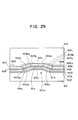
- FIG.29 showing a device having a structure similar to FIG.25.
- the device of FIG.29 will be designated by the same reference numerals for those parts that correspond to the device of FIG.25, and the description thereof will be omitted.
- the clad layer 406 is divided into a lower layer 406, and an upper layer 406 2 , wherein the upper layer 406 2 is doped uniformly to the n-type by incorporation of Se, while the lower layer 406, is doped simultaneously by Zn and Se such that the layer 406, has a first region 61 a of the n-type that is laterally sandwiched by a pair of second regions 61 b i and 61 b 2 of the p-type.
- FIG.30 shows a modification of the fifth embodiment wherein the laser diode has a structure similar to the device of FIG.26, except that the clad layer 425 2 is divided into a lower layer 425 21 doped to the n-type by Se and an upper layer 425 22 doped by Zn and Se simultaneously, wherein the layer 425 22 is divided into a first region 425 22 a of the n-type corresponding to the (100) stripe of the mesa structure and a pair of regions 425 22 b 1 and 425 22 b 2 of the p-type formed at both sides of the region 425 22 in correspondence to the (311)A surface.
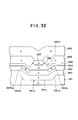
- FIG.31 shows another modification of the fifth embodiment wherein the laser diode has a structure similar to the device of FIG.27, except that the clad layer 444 2 is divided into a lower layer 444 2 , doped to the n-type by Se and an upper layer 444 22 that is doped simultaneously by Zn and Se.
- the upper layer 444 22 is divided into a first region 444 22 a corresponding to the (100) stripe of the mesa structure and doped to the n-type and a pair of regions 444 22 bi and 444 22 b 2 corresponding to the (311)A surface and doped to the p-type.
- the device is constructed on an n-type substrate 461 of GaAs.
- the substrate 461 is formed with a negative mesa structure 461 a that is defined by a (100) stripe surface 461 c at the bottom surface and a pair of (311)A surfaces 461 1 and 461 b 2 that form the side wall of the mesa structure 461 a.
- a buffer layer 462 of n-type GaAs is grown epitaxially.
- the second mesa structure in the buffer layer 462 in correspondence to the mesa structure 461 a such that the second mesa structure has a (100) oriented stripe surface at the bottom and a pair of (311)A oriented side walls that define the (100) oriented stripe surface at the bottom.
- a clad layer 463 of n-type InGaAIP is grown epitaxially while doping simultaneously by Zn and Se such that a pair of p-type regions designated as 463b i and 463b 2 are formed in the layer 462 in correspondence to the (311)A surface.
- the rest of the layer 463 is doped to the n-type.
- an active layer 464 of undoped InGaP is grown epitaxially on the clad layer 463, and a p-type clad layer 465 of InGaAIP is grown further on the active layer 454.
- the clad layer 465 is formed with a positive mesa structure 465a that projects upward in correspondence to the negative mesa structure 461a, and an intermediate layer 466 of p-type InGaP is grown in correspondence to the mesa structure 465a. Further, another intermediate layer 467 of p-type GaAs is formed on the layer 466 as a continuation of the mesa structure 465a.
- the mesa structure 465a including the InGaP layer 466 and the GaAs layer 467 grown thereon are laterally supported by an n-type region 468 of GaAs for current confinement, and a p-type contact layer 469 of GaAs is grown on the layer 468 in contact with the upper major surface of the layer 467.
- the mesa structure 465a in correspondence to the clad layer 465, the effect of the current confinement is increased even more.
- FIG.32 Next, the fabrication process of the structure of FIG.32 will be described briefly with reference to FIGS.33(A) - 33(M).
- the mesa structure 461 a is formed on the upper major surface of the n-type substrate 461 as a groove extending in the (011) direction such that the groove is defined by the bottom surface 461 c and a pair of side walls 461b, and 461 b 2 . Further, the epitaxial growth of the n-type GaAs layer 462 is achieved on the structure thus obtained such that the second mesa structure is formed in correspondence to the mesa structured 461 c such that the mesa structure is laterally defined by a pair of (311)A side walls as shown in FIG.33(B).
- the layers 463 through 467 are grown consecutively by the MOCVD process with respective conductivity types as shown in FIG.33(C).
- the layer 463 is doped to the n-type except for the obliquely extending surface part that is doped to the p-type, while the layers 465 - 467 are doped to the n-type.
- a silicon oxide mask 471 is deposited on the upper major surface of the layer 467 as shown in FIG.33(D), and a photoresist 471 is deposited on the mask 471. It should be noted that there is formed a depression or groove on the upper major surface of the layer 467 and hence on the upper major surface of the layer 471 in correspondence to the mesa structure 461c, and the photoresist fills the groove thus formed.
- the photoresist 472 is subjected to an ashing process using oxygen plasma, such that the photoresist 472 is removed except for those parts that fills the groove.
- the silicon oxide mask 471 is subjected to an etching process while using the remaining photoresist 472 as a mask, and the photoresist 472 is removed subsequently as shown in FIG.33(G).
- FIG.33(G) is subjected to a wet etching process using an aqueous solution of NH 4 and H 2 0 2 as the etching agent, wherein the layer 467 is etched selectively as shown in FIG.33(H). Further, the silicon oxide layer 471 projecting outward form the patterned layer 467 is removed by a wet etching process that uses a buffered HF solution as the etching agent as shown in FIG.33(1).
- the intermediate layer 466 is removed by a wet etching process using a mixture of Br, HBr and H 2 0 while using the patterned layer 467 as a mask, and the layer 465 is etched subsequently by using a HCI etching solution. Thereby, the structure shown in FIG.33(J) is obtained.
- the deposition of n-type GaAs is achieved by the MOCVD process to form the GaAs layer 468 as shown in FIG.33(K). Further, the mask 471 is removed in the step of FIG.33(L), and the p-type GaAs contact layer 469 is deposited on the structure of FIG.33(L) as shown in FIG.33(M). Thereby, the structure of FIG.32 is obtained.
- FIG.34 shows a stripe laser diode according to the seventh embodiment, wherein the device is constructed on a GaAs substrate 501 doped by Si to the n-type with the carrier concentration level of 4 X 10 18 cm -3 .
- the substrate 501 has a (100)-oriented upper major surface as usual, wherein the upper major surface is formed with a step 501 a that extends in the longitudinal direction of the laser diode coincident to the ⁇ 01 1 > direction of GaAs crystal.
- the step 501 a is formed of a (311)A oriented stripe surface 501 c extending in the foregoing (011) direction with a step height of typically 1 ⁇ m, and the step 501a divides the upper major surface of the substrate 501 to a first (100) region 501b, and a second (100) region 501 b 2 .
- the step 501 a can be formed on the planar (100) surface of the GaAs substrate 501 by providing a silicon oxide mask and apply a wet etching process using a HF solution as the etching agent.
- the concentration level of Se is changed depending on the crystal surface as already explained with reference to FIG.17.
- the Se concentration level is about 3 X 10 17 cm -3 on the part grown on the (100) surface, while the Se concentration level changes to about 1.2 X 10 17 cm -3 in correspondence to the part grown on the (311)A surface. See the relationship of FIG.17.
- the stepped structure of the upper major surface of the substrate 501 is transferred to the upper major surface of the buffer layer 502.
- an intermediate layer 503 of n-type InGaP is grown epitaxially by a MOCVD process.
- the layer 503 has a composition of Ga o . 5 1n o . 5 P and doped by Se or Si, wherein the concentration level of Se changes, when Se is used for the dopant, depending on the crystal surface such that the Se content takes a value of 3.7 X 10 17 cm -3 on the (100) surface while a value of about 7 X 10 16 cm- 3 on the (311)A surface.
- the thickness of the layer 503 becomes about 0.1 ⁇ m on the (100) surface while the thickness is about 0.25 ⁇ m on the (311)A surface.
- a clad layer 504 of n-type InGaAIP is grown with a composition of (Al 0.7 Ga 0.3 ) 0.5 In 0.5 P, wherein the layer 504 is doped by Se or Si to the n-type.
- the thickness of the layer 504 may change slightly depending on the crystal surface such that the layer 504 has a thickness of about 0.3 ⁇ m for the part grown on the (100) surface while the layer 504 has a thickness of about 0.6 ⁇ m for the part grown on the (311)A surface.
- an optical guide layer 505 of n-type InGaAIP is grown on the layer 504 with a composition of (Al 0.4 Ga 0.6 ) 0.5 In 0.5 P, wherein the layer 505 is doped by Se or Si to the n-type.
- the thickness of the layer 505 changes depending on the crystal surface on which the layer is grown such that the part of the layer 505 grown on the (100) surface has a thickness of 0.2 ⁇ m while the part grown on the (311)A surface has a thickness of about 0.4 ⁇ m.
- an active layer 506 of undoped InGaP is grown on the layer 505 with a composition of Ga o . 5 1n o . 5 P.
- the thickness of the layer 506 changes depending on the crystal surface on which the layer is grown such that the part of the layer 506 grown on the (100) surface has a thickness of 0.015 ⁇ m while the part grown on the (311)A surface has a thickness of 0.03 ⁇ m.
- a p-type clad layer 507 of InGaAIP is grown with a composition of (Al 0.7 Ga 0.3 ) 0.5 In 0.5 P.
- the layer 507 is doped by Mg or Zn and has a thickness of 0.3 ⁇ m in correspondence to the part grown on the (100) surface and a thickness of 0.6 ⁇ m in correspondence to the part grown on the (311)A surface.
- another clad layer 508 of InGaAIP is grown on the layer 507 while doping simultaneously by Zn and Se such that the layer 507 is divided into a p-type first region 508a having a composition of (Al 0.7 Ga 0.3 ) 0.5 In 0.5 P and a thickness of 0.4 ⁇ m and a pair of n-type second regions 508bi and 508b 2 located at both sides of the region 508a with a thickness of 0.2 ⁇ m.
- the region 508a is enriched in Zn than Se and shows the p-type conductivity type while the regions 508b i and 508b 2 are enriched in Se than Zn and shows the n-type conductivity type.
- an intermediate layer 509 of p-type InGaAIP having a composition of (Al o .,Ga o .g)- 0.5 In 0.5 P is grown with a thickness of 0.04 ⁇ m in correspondence to the part grown on the (100) surface and a thickness of 0.08 ⁇ m in correspondence to the part grown on the (311)A surface.
- another intermediate layer 510 of p-type InGaAIP is grown on the layer 509 with a composition of (Al 0.4 Ga 0.6 ) 0.5 In 0.5 P such that the layer 510 has a thickness of 0.1 ⁇ m in correspondence to the part grown on the (100) surface and a thickness of 0.2 ⁇ m in correspondence to the part grown on the (311)A surface.
- both the layers 509 and 510 are doped by Mg or Zn and shows the p-type conductivity irrespective of the crystal surface.
- a contact layer 511 of p-type GaAs is provided on the layer 510 with a thickness of 5 - 10 ⁇ m.
- the layer 511 may be doped by Zn with a concentration level of 1 - 6 X 10 18 cm -3 .
- doping is achieved by admixing the gaseous material containing the desired dopant into the source gas of the epitaxial layer similarly to the previous embodiments.
- Se alone is introduced as in the layers 502 - 505
- hydrogen selenide is added for example with a mole ratio of Se with respect to the group V elements set to about 2 X 10- 6 such that an electron concentration level of about 8 X 10 17 cm -3 is achieved on the part grown on the (100) surface and an electron concentration level of about 1.5 X 10 17 cm -3 in correspondence tot he part grown on the (311)A surface.
- the mole ratio of dimethylzinc used for the source of Zn is set to 0.1 with respect to the gaseous source of the group III elements, wherein dimethylzinc is supplied with a concentration level such that the Zn content in the layer 508 becomes to about 5 X 10 16 cm -3 in correspondence to the part grown on the (100) surface and such that the Zn content becomes to about 5 X 10 17 cm -3 in correspondence to the part grown on the (311)A surface.
- an upper electrode 512 and a lower electrode 513 are provided respectively on the upper major surface of the GaAs contact layer 511 and a lower major surface of the GaAs substrate 501.
- the device of FIG.34 too, one can obtain an efficient current confinement in the region 508a and an efficient laser oscillation is obtained in the active layer in correspondence to the stripe region grown on the (311)A surface.
- the device is formed by a simple repetition of the epitaxial process once the substrate 501 is formed with the step 501 a.
- FIG.35 shows a modification of the device of FIG.34, wherein a remote junction is formed within the clad layer 507.
- the layer 507 is formed of a lower layer part 507, and an upper layer part 507 2 , wherein the lower layer part 507, is divided into a first region 507a of p-type formed in correspondence to the (311)A surface and a pair of second regions 507bi and 507b 2 , both doped to the n-type.
- Such a doping of the layer 507 is achieved by employing the simultaneous doping of Zn and Se as already described.
- the upper layer part 507 2 is doped to the p-type throughout. With the formation of the remote junction at the interface between the n-type region 507b i or 507b 2 and the p-type upper layer 507 2 , one can enhance the effect of the current confinement further.
- FIG.36 shows another modification of the laser diode of FIG.34, wherein the device is constructed on an n-type GaAs substrate 601 that has an upper major surface 601 b tilted from the (100) surface toward the (111)A surface by about + degrees, wherein the positive angle of tilting indicates the tilting of the surface in the clockwise direction.
- the substrate 601 is formed with a groove or negative mesa 601 a to extend in the (011) direction, wherein the negative mesa 601a a is defined by a (311)A oriented side wall 601 c and an opposing side wall 601 d that is tilted from the (100) surface toward the (111)A surface by a tilt angle of -9 degrees.
- the surface 601 d forms a crystallographically equivalent surface to the upper major surface 601 b of the substrate 601.
- epitaxial layers 602 - 606 are grown consecutively, wherein the layer 602 corresponds to the clad layer 502, the layer 603 corresponds to the active layer 506, the layer 604 corresponds to the clad layer 507, the layer 605 corresponds to the clad layer 508, and the layer 606 corresponds to the layer 509. Further, a contact layer 607 of p-type GaAs is formed on the layer 606 in correspondence to the contact layer 511. On the upper major surface of the layer 607, an upper electrode 608 is formed, while a lower electrode 609 is formed on the lower major surface of the substrate 601.
- the layer 602 is doped to the n-type by Se or Si, while the layers 604 and 606 are doped by Mg or Zn to the p-type, similarly to the previous embodiment.
- the clad layer 605 is doped simultaneously by Zn and Se.
- the clad layer 605, doped by Zn and Se simultaneously is divided into three distinct parts or regions, a first region 605a grown on the (311)A stripe surface, and second and third regions 605bi and 605b 2 formed at both lateral sides of the first region 605a, wherein the first region 605a has the p-type conductivity while the second and third regions 605bi and 605b 2 have the n-type conductivity type.
- the region 605b i forming the side wall of the mesa 601 a has a crystal surface equivalent to the crystal surface of the region 605b 2 that is formed on the upper major surface of the substrate, because of the foregoing tilting of the upper major surface.
- the drive current is confined selectively into the stripe part of the active layer 603 formed in correspondence to the (311)A surface, and the laser oscillation occurs preferentially in this stripe part.
- the laser oscillation in the other stripe part corresponding to the surface 601 d is suppressed because of the depletion of the drive current.
- the principle of the laser diode as set forth in FIG.36 can be applied to the form a structure for avoiding melting of the edge surface in the laser diode known as catastrophic optical damage.
- the laser diodes there is a tendency that impurity states at the edge surface of the laser diode absorbs the optical beam, and such an optical absorption causes a temperature rise at the edge part of the laser diode.
- the band gap of the active layer is narrowed and ultimately cause a short circuit. Thereby, the current flows along the edge surface and induces a melting.
- the conventional high power laser diodes uses a wide band gap material at the edge part.
- the electrode is formed such that the injection of the current does not occur in correspondence to the edge part.
- these conventional measure is complex and not practical for fabricating the laser diode in the actual production line.
- FIGS.37 and 38 show the process for fabricating a laser diode wherein the problem of the catastrophic optical absorption is eliminated, based upon the principle explained with reference to FIG.36.
- a substrate 701 of n-type GaAs is prepared such that the substrate 701 has upper and lower major surfaces characterized by a crystal surface that is tilted with respect to the (100) surface of the GaAs crystal toward the (111)A surface by +8 degrees. Further, the upper major surface of the substrate 701 is covered by a silicon oxide layer 702 that is patterned as shown in FIG.37. There, the oxide layer 702 forms a mask and has a pair of projecting patterns 702a and 702b in correspondence to the both longitudinal edges of the substrate 701.
- FIG.38 shows the state after the mask 702 is removed.
- the upper major surface of the substrate 701 is divided into a first surface 703a forming a stripe region and characterized by the (311)A surface and a pair of flat surfaces 703bi and 703b 2 formed at both sides of the stripe region 703a and characterized by the same tilted crystal surface as the original upper major surface of the substrate 701.
- an oblique surface 704a characterized by the crystal surface offset from the (311)A surface is formed in alignment with the stripe surface 703a such that the surface 704a is laterally bounded by surfaces 704b i and 704b 2 , wherein the surfaces 704, and 704b 2 are formed by the same crystal surface as the tilted upper major surface 703b i or 7093b 2 of the substrate 701.
- epitaxial layers are grown by the MOCVD process similarly to the device of FIG.36.
- the epitaxial layer grown on the stripe surface 703a is not equivalent to the epitaxial layer grown on the stripe surface 704a.
- the relationship between the epitaxial layer grown on the stripe surface 703a and epitaxial layer grown on the stripe surface 704a is similar to the relationship between the epitaxial layer 605a and the epitaxial layer 605b i of FIG.36.
- FIG.39 shows the essential part of the epitaxial layers grown on the structure of FIG.38, wherein an n-type InGaAIP clad layer 705a, an undoped InGaP active layer 706a and a p-type InGaAIP clad layer 707a are grown consecutively on the essential part of the structure of FIG.39 including the surfaces 703a and 703bi, 703b 2 .
- the clad layer 705a is doped by Se to the n-type throughout, while the layer 707a is doped simultaneously by Zn and Se such that the part of the layer 707a grown on the (311)A surface is doped to the p-type while the rest of the layer 707a is doped to the n-type.
- epitaxial layers 705b - 707b are grown consecutively on the edge part of the structure of FIG.38 including the surfaces 704a, 704bi and 704b 2 simultaneously to the corresponding layers 705a - 707a, wherein it will be noted that none of these surfaces include the (311)A surface.
- the clad layers 705b and 707b are both doped to the n-type and the double hetero junction essential for the laser diode is no longer formed in the edge part of the laser diode. Thereby, the laser oscillation at the edge part of the laser diode is prohibited even when the electrode is provided uniformly on the upper and lower major surface of the laser diode structure thus formed, and the problem of the catastrophic optical damage is avoided successfully.
Landscapes
- Physics & Mathematics (AREA)
- Optics & Photonics (AREA)
- Engineering & Computer Science (AREA)
- Condensed Matter Physics & Semiconductors (AREA)
- General Physics & Mathematics (AREA)
- Electromagnetism (AREA)
- Manufacturing & Machinery (AREA)
- Computer Hardware Design (AREA)
- Microelectronics & Electronic Packaging (AREA)
- Power Engineering (AREA)
- Geometry (AREA)
- Semiconductor Lasers (AREA)
Abstract
Description
- The present invention generally relates to laser diodes and more particularly to an improvement of a laser diode having a stripe structure.
- With the widespread use of laser diodes in various fields of human society such as optical storage of information in optical disk systems, optical reading of bar codes in POS systems, optical recording of images in printers, and the like, there is an increasing demand for a laser diode that produces short wavelength optical beam in the visual wavelength band. With the use of such a short wavelength radiation for the optical beam, one can increase the storage capacity of the optical information storage system. Further, the use of visible light is advantageous in other applications such as the POS systems.
- In the optical information storage systems that record and reproduce information on and from a recording media by means of a finely focused optical beam, the laser diode is required to have a small astigmatism in addition to the usual requirement of low threshold current, high output power and high reliability. In the optical information storage systems in particular, the optical beam is required to have a very small round beam shape when focused on a recording medium such as an optical disk. When there is a large astigmatism in the laser diode, the optical beam does not form the desired round beam spot but forms an elongated spot wherein the direction of elongation changes depending on the focusing state. In order to eliminate or minimize the problem of astigmatism, various efforts have been made so far.
- FIG.1 shows the basic structure of a typical conventional laser diode of the so-called ridge type that produces an output optical beam in the visible wavelength region.
- Referring to FIG.1, the laser diode is constructed on the (100)-oriented upper major surface of a
GaAs substrate 101 doped to the n-type. There, abuffer layer 102 of n-type GaAs is grown epitaxially on the (100)-oriented surface of theGaAs substrate 101, and anintermediate layer 103 of n-type InGaP is grown further on thebuffer layer 102 epitaxially. - On the
intermediate layer 103, aclad layer 104 of n-type InGaAIP is grown epitaxially, and anactive layer 105 of undoped InGaP is grown epitaxially on theclad layer 104. Theactive layer 105 in turn is covered by aclad layer 106 of p-type InGaAIP, and anetching stopper layer 107 of p-type InGaP is grown on theclad layer 106. Further, a clad layer 109 of p-type InGaAIP and an intermediate layer 110 of InGaP are grown consecutively to form a layered semiconductor body, and a silicon oxide layer (not shown) is deposited further on the layer 110. Next, the silicon oxide layer is patterned in correspondence to the ridge structure to be formed to form a patterned silicon oxide mask, and the layered semiconductor body obtained previously is subjected to a wet etching process while using the patterned silicon oxide mask. Thereby, a ridge structure including the layers 109 - 110 is formed on theetching stopper layer 107. Further, while using the same silicon oxide mask, a deposition of n-type GaAs is made such that the foregoing ridge structure is laterally supported by a pair of n-type GaAs regions formed as a result of the foregoing deposition of n-type GaAs. - In the laser diode of FIG.1, the layers 109 - 111 form a ridge structure supported laterally by the n-
type GaAs regions 108a and 108b as already noted, and the ridge structure thus constructed forms a loss guide structure for guiding therethrough the optical beam produced in theactive layer 105. There, the GaAs regions at both sides of the ridge structure absorbs the optical beam and changes the refractive index in response thereto. It should be noted that the band gap of GaAs is much smaller than the band gap of InGaP or InGaAIP. Further, such a ridge structure, supported laterally by the p-type GaAs regions 108a and 108b, causes a confinement of the drive current within the ridge. Thereby, the laser diode of FIG.1 is characterized by a low threshold current. By using InGaP for the material of theactive layer 105, one can realize a laser oscillation at the wavelength of about 680 nm. Thus, the laser diode of FIG.1 is capable of producing output optical beam with a visible wavelength. - The laser diode of FIG.1, however, has a problem in that there appears an astigmatism in the optical beam produced from the device. More specifically, there arises a discrepancy in the focal point of the optical beam that is emitted at the edge surface of the laser diode with a horizontal plane of beam divergence and the optical beam that is emitted at the same edge surface with a vertical plane of beam divergence. FIG.2 shows such a situation wherein two focal points, f1 and f2, exist in the optical beam produced from the laser diode. There, the optical beam spreads in the vertical plane from the first focal point fi, while the optical beam spreads in the horizontal plane from the second focal point f2, wherein the focal point f2 is offset from the focal point f1 by several microns. Associated with such an offset in the focal point, the beam spot of the optical beam has an elongated elliptical shape that is not desirable for optical storage of information such as the optical disk systems as already described. It will be noted that the direction of elongation of the elliptical beam spot changes depending on the focusing state of the optical beam.
- The foregoing astigmatism occurring in the laser diode of FIG.1 is caused mainly by the difference in the degree of optical confinement between the vertical plane and the horizontal plane. As long as the loss guide structure that lacks the refractive structure for efficient lateral optical confinement is used, one cannot avoid the problem of astigmatism. In order to overcome or minimize the astigmatism, the inventors of the present invention have proposed previously in the European Laid-open Patent Publication
EP 0 454 476 that corresponds to the United States Patent Applications S.N.691,620 now abandoned and S.N.892,680 that is a file-wrapper continuation of the former, a laser diode having a stripe structure wherein an active layer is provided to extend as a stripe in correspondence to a mesa structure that is formed on a substrate on which the laser diode is constructed. - FIG.3 shows the laser diode proposed previously by the present inventors.
- Referring to FIG.3, the laser diode is constructed on a
GaAs substrate 201 doped for example to the p-type. Thesubstrate 201 has a (100)-oriented upper major surface, and a mesa structure 201 a that is characterized by a (100)-oriented upper major surface and a pair of (111 )B-oriented side walls, is formed on the upper major surface as illustrated. It should be noted that the (100) surface of the mesa structure 201 a extends in the longitudinal direction of the laser diode and forms the basis of the stripe structure. - On the
substrate 201 thus shaped, acurrent confinement layer 202 of n-type GaAs is grown epitaxially while protecting the upper major surface of the mesa structure 201 a by a mask such as silicon oxide. When an epitaxial process is applied to the (111)B surface that extends obliquely to the (100) surface of theGaAs substrate 201, it is known that a (311)B surface develops preferentially because of the slow rate of crystal growth in this crystal orientation. In other words, theepitaxial layer 202 thus grown is characterized by the well-developed (311)B surface that extends obliquely to the (100) surface of GaAs at both sides of the mesa structure 201a. Thereby, the (311)B surface forms another mesa structure that extends coincident to the stripe structure of the laser diode. - After the
layer 202 is formed and the mask removed, abuffer layer 203 of p-type GaAs is grown epitaxially for providing an improved crystal surface for the subsequent epitaxial processes, and anintermediate layer 204 of p-type InGaP corresponding to the intermediate layer 110 is grown further on thebuffer layer 203. Further, aclad layer 205 of p-type InGaAIP is grown epitaxially on theintermediate layer 204, and an active layer of undoped InGaP is grown epitaxially on theclad layer 205. - On the
active layer 205, aclad layer 207 of n-type InGaAIP is grown epitaxially, and anintermediate layer 208 of n-type InGaP corresponding to theintermediate layer 103 of FIG.1 is grown further thereon. Further, acontact layer 208 of n -type GaAs is grown on the intermediate layer 110 epitaxially, and upper and lower electrode layers (not shown) are provided respectively on the upper major surface of thecontact layer 209 and the lower major surface of thesubstrate 201. The epitaxial layers are grown by the MOCVD process for exact control of composition, and dopants are incorporated into the epitaxial layers as necessary during the epitaxial process. Usually, Zn is used for the p-type dopant, while Se or Si is used for the n-type dopant. Zn may be incorporated by admixing dimethylzinc ((CH3)2Zn) to the source gas of the epitaxial layers, while Se is incorporated by admixing hydrogen selenide (H2Se). When Si is used, a gas of silane (SiH4) or disilane Si2He) is used. - In operation, a forward bias voltage is applied across the upper and lower electrodes to inject carriers into the
active layer 206. In the illustrated example, holes are injected into the p-type substrate 201 and transported to theactive layer 206 through the mesa structure 201 a due to the current confinement that is achieved by the n-type GaAs layer 202 at both sides of the mesa structure 201 a. Thereby, the holes are injected preferentially at the central part of theclad layer 205 and transferred further to theactive layer 206 for recombination with electrons that are injected from the upper electrode and transported to theactive layer 206 via the layers 209 - 207. Such a recombination of electrons and holes initiates the well known stimulated emission process, and the stimulated emission process causes an amplification of the optical beam when reflectors are provided at both longitudinal ends of the laser diode for reflecting the optical beam back and forth through the laser diode. Thereby, one obtains a laser oscillation as is well known in the art. - In the structure of the laser diode thus fabricated, it should be noted that the
layers 203 through 209 are all formed in conformity with the surface morphology of the second mesa structure in that each layer includes an elongated stripe region characterized by a (100) surface and extending in correspondence to the (100) surface of the mesa structure 201a. There, each stripe region is laterally defined by a pair of lateral regions located at both sides of the elongated (100) stripe surface and characterized by the (311)B surface in correspondence to the (311)B surface of thelayer 202. Of course, the (100) surface is flat and extend parallel with the upper major surface of the mesa structure 201 a, while the (311)B surface extends obliquely to the (100) surface. Because of the lateral confinement of the optical beam in the stripe region of the active layer wherein the recombination of the carriers occurs predominantly, the problem of astigmatism is successfully eliminated in the device of FIG.3. - In such a structure wherein each epitaxial layer includes crystallographically non-equivalent surfaces, the nature or property of the epitaxial layers changes depending on the orientation of the crystal surface.
- In the laser diode of FIG.3, it will be noted that the
clad layer 205 is formed of three distinct regions characterized by respective, three crystallographically distinct surfaces, the first region characterized by the (100) surface and the second and third regions characterized by the (311)B surfaces, wherein the second and third regions are located at both sides of the first region and extend in the longitudinal direction of the laser diode together with the first region. As will be discussed in detail later, it was discovered that the concentration level of the dopant changes depending on the first through third regions of theclad layer 205. More specifically, the concentration level of Zn is higher in the second and third regions that is characterized by the (311)B surface as compared with the first region that is characterized by the (100) surface. Associated with such a variation in the concentration of the dopant, there appears a variation in the carrier density such that the density or concentration level of the holes is higher in the second and third regions as compared with the first region. This indicates that the resistivity of theclad layer 205 increases in the first region as compared with the second and third regions located at both sides thereof because of the reduced concentration of the carriers. Thus, there is a tendency that the injected current flows preferentially through the oblique region of theclad layer 205 rather than the stripe region having the (100) surface as indicated by arrows in FIG.3. In other words, drive current avoids the strip region of theactive layer 206 where the recombination occurs, and the laser diode of FIG.3 has a problem of poor current confinement and hence a low efficiency of laser oscillation. - Further, the conventional laser diode of FIG.3 has a problem of large resistivity due to the relatively small Zn content in the epitaxial layer. More specifically, the small Zn content in the epitaxial layer causes the problem of small concentration of holes in the p-type layers, and the conventional laser diode has suffered from the problem of large resistivity and limited operational power. It should be noted that the laser diode would generate intolerable heat due to the large resistivity of the p-type layers, particularly when the injection current is increased. It is thought that this problem arises from the large vapor pressure of Zn that is in equilibrium with the crystal phase during the MOCVD process. There, Zn tends to concentrate more in the vapor phase than in the crystal as a result of the evaporation, and such a tendency is enhanced when the temperature of the epitaxial process is increased. As it is desirable to use high temperature for obtaining high quality crystal layer in the epitaxial process, the foregoing tendency contradicts with the requirement of large dopant concentration level in the epitaxial layers of the laser diode.
- Accordingly, it is a general object of the present invention to provide a novel and useful process for fabricating a laser diode wherein the foregoing problems are eliminated.
- Another and more specific object of the present invention is to provide a laser diode operational in the visible wavelength with a reduced astigmatism and with an improved current confinement.
- Another object of the present invention is to provide a process for fabricating a laser diode on a substrate that is formed with a stripe structure defined by crystallographically distinct surfaces and extending in a predetermined direction, wherein the device has a reduced resistivity associated with a high dopant concentration level in the clad layer.
- Another object of the present invention is to provide a simple process for forming an effective current confinement structure in a laser diode.
- Another object of the present invention is to provide a process for fabricating a laser diode, comprising the steps of: forming a first stripe structure defined by a plurality of crystallographically distinct surfaces each extending parallel with each other in a predetermined direction on an upper major surface of a semiconductor substrate; forming a layer of InGaAIP on said semiconductor substrate including said first stripe structure by a decomposition of organic source materials of In, Ga, AI and P while maintaining an epitaxial relationship with respect to said semiconductor substrate such that said layer of InGaAIP is formed with a second stripe structure corresponding to said first stripe structure, said layer of InGaAIP being formed such that said second stripe structure is formed of a plurality of crystallographically distinct surfaces corresponding to said plurality of crystallographically distinct surfaces that form said first stripe structure; and doping said InGaAIP layer to the p-type by incorporating Mg while growing said InGaAIP by admixing a gaseous source material of Mg into said source materials of In, Ga, AI and P such that said InGaAIP layer is doped to the p-type with a substantially uniform carrier concentration level irrespective of the crystal surfaces forming said second stripe structure. According to the present invention, one can obtain a relatively uniform distribution of Mg in the clad layer irrespective of the crystal surface on which the clad layer is grown. In other words, the uniform distribution of Mg is achieved even when the clad layer is formed on the stripe structure that includes crystallographically distinct surfaces, contrary to the conventional process wherein Zn is used for the dopant. The present invention is particularly useful for eliminating the spreading of the drive current in the stripe laser diodes wherein the GaAs substrate is formed with such a stripe structure. Further, the use of Mg as the p-type dopant enables a high level doping that is advantageous for reducing the resistivity of the laser diode. By growing the clad layer doped with Mg before an undoped active layer is grown, one can obtain a sharp boundary of conductivity type in correspondence to the interface between the clad layer and the active layer that is grown on the clad layer. By interrupting the supply of Mg, the incorporation of Mg into the clad layer is stopped immediately. On the other hand, when the Mg-doping is applied to the clad layer that is grown on the active layer formed already, there tends to appear a delay in the incorporation of Mg into the clad layer even when the supply of Mg is started, and the boundary of the conductivity type, which is essential for the double-hetero structure of the laser diode, may shift from the physical interface between the active layer and the clad layer.
- Another object of the present invention is to provide a process for fabricating a laser diode, comprising the steps of: forming a first stripe structure defined by a plurality of crystallographically distinct crystal surfaces including the (100) surface on an upper major surface of a semiconductor substrate, each of said crystal surfaces being formed to extend parallel with each other in a predetermined direction of said semiconductor substrate; forming a layer of InGaAIP on said semiconductor substrate including said first stripe structure by a decomposition of organic source materials of In, Ga, AI and P while maintaining an epitaxial relationship with respect to said semiconductor substrate such that said layer of InGaAIP is formed with a second stripe structure corresponding to said first stripe structure, said layer of InGaAIP being formed such that said second stripe structure is formed of a plurality of crystallographically distinct crystal surfaces corresponding to said plurality of crystal surfaces that form said first stripe structure; and doping said InGaAIP layer by incorporating a p-type dopant and an n-type dopant simultaneously while growing said layer of InGaAIP by adding gaseous source materials of said p-type dopant and said n-type dopant into said gaseous source materials of In, Ga, AI and P such that said InGaAIP layer has an electronic property that changes depending on said crystallographically distinctly surfaces of said InGaAIP layer. According to the present invention, one can form a p-type region and an n-type region in the same clad layer simultaneously by a single MOCVD process such that the n-type region is sandwiched laterally by a pair of p-type regions or vice versa. For example, by selecting Mg or Zn as the p-type dopant and by selecting Se as the n-type dopant, one can form the clad layer such that the clad layer includes a p-type stripe region and a pair of n-type stripe regions that sandwich the p-type stripe region laterally or vice versa. Alternatively, one may form the clad layer such that the part of the clad layer grown on said first stripe surface has a carrier density that is substantially larger than the part of the clad layer that is grown on the other stripe surfaces by setting the doping level of the p-type dopant and the n-type dopant appropriately. Thereby, one can achieve an efficient current confinement at the clad layer and the efficiency of laser oscillation is improved substantially. By growing an active layer on the clad layer thus formed, one can achieve an effective lateral confinement of the optical beam in the active layer in correspondence to the stripe structure. More particularly, the morphology of the stripe structure characterized by the crystallographically distinct stripe surfaces is transferred to the clad layer, and the part of the active layer that is grown on the first stripe surface of the clad layer is supported laterally by a pair of sloped surfaces of the clad layer that are formed in correspondence to other stripe surfaces with an angle with respect to the first stripe surface. In other words, the optical radiation produced in the active layer is confined therein laterally by the first or second clad layer, and the problem of astigmatism is substantially eliminated.
- Another object of the present invention is to provide a process for fabricating a laser diode, comprising the steps of: forming a crystal surface on an upper major surface of a semiconductor substrate such that said crystal surface has a crystal orientation different from said upper major surface; and forming a clad layer on said substrate while maintaining an epitaxial relationship between said clad layer and said substrate; wherein said step of forming the clad layer comprises a step of incorporating a p-type dopant and an n-type dopant simultaneously. According to the present invention, one can obtain a clad layer wherein the conductivity type is changed selectively therein by a single deposition step. Thereby, one can fabricate a laser diode having an excellent confinement of current easily.
- Another object of the present invention is to provide a stripe laser diode, comprising: a substrate of a semiconductor material having an upper major surface and a lower major surface and extending in a longitudinal direction from a first end to a second, opposite end; a stripe structure formed on said upper major surface of said substrate as a part of said substrate, said stripe structure comprising a first stripe surface formed of the (100) surface and extending in said longitudinal direction and a pair of different stripe surfaces each having a crystal orientation different from the (100) surface and extending in said longitudinal direction at both lateral sides of said first stripe surface; a first clad layer of InGaAIP doped provided on said substrate to extend in said longitudinal direction from a first end to a second, opposite end, said first clad layer having upper and lower major surfaces and including a stripe structure formed therein in conformity with said stripe structure of said substrate; an active layer of undoped semiconductor material having a band gap smaller than said first clad layer and provided on said first clad layer to extend in said longitudinal direction from a first end to a second, opposite end, said active layer having upper and lower major surfaces and including a stripe structure formed therein in conformity with said stripe structure of said substrate; a second clad layer of InGaAIP provided on said active layer to extend from said first end to said second end of said substrate, said second clad layer including a stripe structure formed therein in conformity with said stripe structure of said substrate; first carrier injection means provided on said lower major surface of said substrate for injecting first type carriers having a first polarity to said active layer via said first clad layer by establishing an ohmic contact therewith; and second carrier injection means provided on said upper major surface of said second clad layer for injecting second type carriers having a second, opposite polarity to said active layer via said second clad layer; one of said first and second clad layers being doped to the p-type by incorporating Mg such that Mg distributes substantially uniformly irrespective of existence of said stripe structure; the other of said first and second clad layers being doped to the n-type. According to the present invention, one can eliminate the problem of leak of the injection current away from the stripe structure wherein the recombination occurs preferentially, by employing Mg that distributes uniformly in the clad layer irrespective of the existence of the stripe structure, as the dopant. Thereby, an efficient laser oscillation can be achieved. As Mg can be doped into the clad layer with increased concentration level as compared with Zn, one can increase the conductivity of the laser diode with respect to the drive current. As the stripe structure of the active layer is laterally sandwiched by the first or second clad layer in the stripe laser diode, one can minimize the problem of astigmatism.
- Another object of the present invention is to provide stripe laser diode, comprising: a semiconductor substrate doped to a first conductivity type, said substrate having an upper major surface and a lower major surface and extending in a longitudinal direction of the laser diode from a first end to a second, opposite end; a first stripe structure formed on said upper major surface of said semiconductor substrate as a part of said substrate, said first stripe structure comprising a first stripe surface formed of the (100) surface and extending in said longitudinal direction and a pair of side surfaces each formed of a crystal surface different from the (100) surface and extending in said longitudinal direction at both lateral sides of said first stripe surface; a first clad layer of InGaAIP having upper and lower major surfaces and provided on said semiconductor substrate to extend in said longitudinal direction from a first end to a second, opposite end; a second stripe structure formed on said upper major surface of said first clad layer to extend in said longitudinal direction as a part of said first clad layer and in conformity with said first stripe structure, said second stripe structure comprising a second stripe surface formed of the (100) surface and extending in said longitudinal direction and a pair of stripe surfaces each formed of a crystal surface different from the (100) surface and extending in said longitudinal direction at both lateral sides of said second stripe surface; an active layer of undoped semiconductor material having upper and lower major surfaces and provided on said first clad layer to extend in said longitudinal direction from a first end to a second, opposite end, said active layer being supplied with first type carriers of a first polarity and second type carriers of a second opposite polarity for producing an optical beam as a result of recombination of said first and second type carriers; a third stripe structure formed on said upper major surface of said active layer to extend in said longitudinal direction as a part of said active layer and in conformity with said first and second stripe structures, said third stripe structure comprising a third stripe surface formed of the (100) surface and extending in said longitudinal direction and a pair of stripe surfaces each formed of a crystal surface different from the (100) surface and extending in said longitudinal direction at both lateral sides of said third stripe surface; a second clad layer of InGaAIP having upper and lower major surfaces and provided on said active layer to extend in said longitudinal direction from said first end to said second end of said substrate; a fourth stripe structure formed on said upper major surface of said second clad layer to extend in said longitudinal direction as a part of said second clad layer and in conformity with said first through third stripe structures, said fourth stripe structure comprising a fourth stripe surface formed of the (100) surface and extending in said longitudinal direction and a pair of stripe surfaces each formed of a crystal surface different from the (100) surface and extending in said longitudinal direction at both lateral sides of said fourth stripe surface; first carrier injection means provided on said lower major surface of said substrate for injecting first type carriers having a first polarity into said active layer via said first clad layer; and second carrier injection means provided on said upper major surface of said second clad layer for injecting said second type carriers having a second, opposite polarity into said active layer via said second clad layer; one of said first and second clad layers being doped with Zn and simultaneously with Se and forming a current blocking structure for guiding a drive current of the laser diode such that said drive current is injected selectively into said active layer in correspondence to the third stripe structure characterized by the third stripe surface. According to the present invention, one can block the injection current at the first and second clad layers such that the injected current flows to the active layer selectively through said first stripe region by setting the concentration level of the p-type dopant and the n-type dopant such that the carrier concentration level increases at said first stripe region or such that the conductivity type changes at said first stripe region. Thereby, an efficient confinement of the injection current is achieved.
- Other objects and further features of the present invention will become apparent from the following detailed description when read in conjunction with the attached drawings.
-
- FIG.1 is a diagram showing the structure of a conventional ridge type laser diode that uses the loss guide structure in a transversal cross section;
- FIG.2 is a diagram showing the astigmatism occurring in the optical beam produced by the laser diode of FIG.1;
- FIG.3 is a diagram showing the structure of a conventional stripe laser diode proposed previously by the inventors in a transversal cross section;
- FIG.4 is a diagram showing the relationship between the doping efficiency and the crystal surface of an InGaAIP crystal for Mg and Zn;
- FIG.5 is a diagram showing the relationship between the doping efficiency and the crystal surface of an InGaAIP crystal for Se;
- FIG.6 is a diagram showing the relationship between the hole concentration and the composition of the organic source materials used for growing InGaAIP, with respect to the (100) surface;
- FIG.7 is a diagram showing the relationship between the Zn and hole concentration and the composition of the organic source materials used for growing InGaAIP, with respect to various crystal surfaces;
- FIG.8 is a diagram showing the dependence of the hole concentration and resistivity on the different crystal surfaces of InGaAIP achieved by the doping of Zn;
- FIG.9 is a diagram showing the dependence of the hole concentration and resistivity on the different crystal surfaces of InGaAIP achieved by the doping of Mg;
- FIG.10 is a diagram showing the structure of the stripe laser diode according to a first embodiment of the present invention in a perspective view;
- FIGS.11 (A) and 11 (B) are diagrams showing the sequence of doping with the growth of the epitaxial layers for forming the structure of FIG.10;
- FIGS.12(A) - 12(D) are diagrams showing the process for constructing the device of FIG.10;
- FIGS.13(A) and 13(B) are diagrams showing the dependence of carrier concentration and resistivity on the different crystal surfaces of InGaAIP achieved by the simultaneous doping of Mg and Se;
- FIG.14 is a diagram showing the structure of a stripe laser diode of a second embodiment of the present invention fabricated according to the principle of FIGS.13(A) and 13(B) in a transversal cross section;
- FIGS.15(A) and 15(B) are diagrams showing the dependence of the carrier concentration level and the resistivity on the various crystal surfaces of InGaAIP achieved by the simultaneous doping of Zn and Se;
- FIG.16 is a diagram showing the relationship between the doping efficiency and the crystal surface of a GaAs crystal for Zn;
- FIG.17 is a diagram showing the relationship between the doping efficiency and the crystal surface of a GaAs crystal for Se;
- FIG.18 is a diagram showing the principle for changing the conductivity type of GaAs depending on the crystal surface thereof based upon the relationship of FIGS.16 and 17;
- FIG.19 is a diagram showing the structure of a stripe laser diode according to a third embodiment of the present invention wherein the principle of FIG.18 is used in a transversal cross section;
- FIG.20 is a diagram showing the stripe laser diode according to a modification of the third embodiment;
- FIG.21 is a diagram showing the stripe laser diode according to another modification of the third embodiment;
- FIGS.22(A) and 22(B) are diagrams showing the process for fabricating the device of FIG. 21;
- FIG.23 is a diagram showing the relationship between the carrier concentration level and the crystal surface for an InGaAIP crystal doped simultaneously by Se and Zn;
- FIGS.24(A) and 24(B) are diagrams showing the concentration of dopants achieved in various crystal surfaces based upon the relationship of FIG.23;
- FIG.25 is a diagram showing the structure of a stripe laser diode according to a fourth embodiment of the present invention;
- FIG.26 is a diagram showing the structure of a stripe laser diode according to a modification of the device of FIG.25;
- FIG.27 is a diagram showing the structure of a stripe laser diode according to another modification of the device of FIG.25;
- FIG.28 is a diagram showing the structure of a stripe laser diode according to still other modification of the device of FIG.25;
- FIG.29 is a diagram showing the structure of a stripe laser diode according to a fifth embodiment of the present invention;
- FIG.30 is a diagram showing the structure of a stripe laser diode according to a modification of the device of FIG.29;
- FIG.31 is a diagram showing the structure of a stripe laser diode according to another modification of the device of FIG.29;
- FIG.32 is a diagram showing the structure of a stripe laser diode according to a sixth embodiment of the present invention;
- FIGS.33(A) - 33(M) are diagrams showing the process for fabricating the device of FIG.32;
- FIG.34 is a diagram showing the structure of a stripe laser diode according to a seventh embodiment of the present invention in a transversal cross section;
- FIG.35 is a diagram showing the structure of a stripe laser diode according to a modification of the device of FIG.34;
- FIG.36 is a diagram showing the structure of a stripe laser diode according to a modification of the device of FIG.34;
- FIGS.37 and 38 are diagrams showing the process for fabricating a laser diode according to an eighth embodiment of the present invention; and
- FIG.39 is a diagram showing the essential part of the laser diode of the eighth embodiment.
- Before starting the description of embodiments, a brief explanation will be given on the experimental evidence that forms the basis of the present invention.
- It is well known that the property or nature of the semiconductor material changes depending on the crystal surface or orientation. This applies not only to the physical property of the crystal known as anisotropy but also to the crystal growth conducted by the epitaxial processes. In the semiconductor layer that is grown by the MOCVD process, in particular, the composition of the semiconductor material tends to change depending on the crystal surface. For example, it is reported that the content of Zn incorporated into the InGaAIP crystal grown by the MOCVD process increases with increasing offset angle of the crystal surface on which the epitaxial growth occurs, with respect to the (100) surface.
- FIG.4 shows the concentration level of Zn and Mg that are added to an epitaxial layer of InGaAIP as a dopant for various crystal surfaces, wherein the data for Zn and Mg is discovered for the first time by the inventors of the present invention (Kondo, M., Anayama, C., Tanahashi, T. and Yamazaki S., Sixth International Conference on Metalorganic Vapor Phase Epitaxy, IEEE Catalog #92TH0459-8, June 8 - 11, 1992). In FIG.4, the data for Zn by other references are also illustrated. There, doping of Mg or Zn is achieved while growing the InGaAIP layer by the MOCVD process, by admixing a gaseous source such as dimethylzinc ((CH3)2Zn) or bis(cyclo-penta-dienyl)magnesium ((CsHs)2Mg) to the source gas of Al, In, Ga and P. In FIG.4, the solid and open circles as well as the solid and open squares represent the data that is obtained by the experiment by the inventors of the present invention, wherein the open circles and open squares represent the result of the SIMS analysis, while the solid circles and solid squares represent the result of the C-V measurement. The condition of the MOCVD process is summarized in TABLE I below.
-

- Referring to FIG.4 showing the Zn content and the Mg content in the InGaAIP layer normalized with respect to the Zn content on the (100) surface, it will be noted that the Zn content increases steeply with increasing tilt angle of the crystal surface toward the (111)A surface (designated as A direction in FIG.4) from the (100) reference surface and then decreases with a further increase of the offset angle, wherein the peak of the Zn concentration appears generally in coincidence to the (311)A surface. It should be noted that the (311) surface that is offset or tilted toward the (111)A surface exposes the Ga surface and hence forms the (111)A surface. On the other hand, the (311) surface tilted toward the (311)B surface exposes the As surface and forms the (311)B surface. When the crystal surface is tilted in the B-direction toward the (311)B surface, on the other hand, it will be noted that the Zn content increases but with a more gentle rate and reaches a maximum at the (311)B surface. When the offset angle is increased more, the Zn content starts to decrease.
- In the case of Mg, it will be noted that the Mg concentration level remains substantially constant even when the crystal surface is tilted toward the (311)B surface. In other words, the content of Mg is substantially the same in the (100) surface and the (311)B surface. When the crystal surface is tilted toward the (311)A surface, on the other hand, the Mg content increases with increasing tilt angle of the crystal surface. Further, it should be noted that the Mg content is much larger than the Zn content in any of the crystal surfaces. As already noted, this reflects the thermodynamic situation in that the equilibrium vapor pressure of Zn is much larger than the that of Mg. In other words, Zn easily escapes from InGaAIP into the vapor phase by causing an evaporation. With increasing deposition temperature, this tendency of depletion of Zn becomes even more conspicuous.
- FIG.5 shows the content of Se incorporated into the InGaAIP layer for various crystal surfaces. There, the growth of the InGaAIP layer is achieved by the MOCVD process with the condition identical with the condition of TABLE I. In FIG.5, it will be noted that the Se content increases slightly in the (311)B surface as compared with the (100) surface and increases steeply when the offset angle exceeds the angle corresponding to the (311)B surface. In the A direction, the Se content decreases steeply with increasing offset angle from the (100) surface.
- FIG.6 shows the effect of Mg doping on the (100) surface of the InGaAIP crystal. There, it will be noted that one obtains the hole concentration level of about 4 X 1017cm-3 by setting the mole ratio of the (CsHs)-2 Mg gas with respect to the source gases of the group III elements, to about 3 X 10⁻⁴. When the desirable hole concentration is about 1 X 10¹⁸ CM-3, the mole ratio may be set to 1 X 10⁻³cm-3. It should be noted that Mg occupies the site of the group III elements in the crystal of InGaAIP and acts as the p-type dopant that releases a hole.
- FIG.7 is a diagram similar to FIG.6 and shows the effect of Zn doping on the various crystal surfaces of InGaAIP. As will be noted in FIG. 7, the Zn content increases with increasing mole ratio of the Zn source gas and changes depending on the crystal surfaces. There, the concentration level of the holes is much smaller than that of Mg shown in FIG.6 in conformity with the result of FIG.4.
- When the Zn doping is used in the growth of the p-type clad
layer 205 of the device of FIG.3, it will be noted from the result of FIG.4 that the oblique part of thelayer 205 that is grown on the (311)B surface, is doped with a larger concentration level of Zn as compared with the flat part grown on the (100) surface as illustrated in FIG.8. Thereby, the carrier density decreases in correspondence to the (100) part that forms the stripe structure, and the resistivity of theclad layer 205 increases in correspondence to the stripe part on which the essential part of the active layer is formed. Thereby, the current injected at the bottom electrode inevitably circumvents the stripe part of theactive layer 206 wherein the recombination of carriers should occur, and the efficiency of the laser oscillation is deteriorated inevitably. - The result of FIG.4 indicates further that the problem of unwanted increase of the resistivity of the InGaAIP layer in correspondence to the (100) surface can be eliminated when the Mg doping is applied in place of the Zn doping. FIG.9 shows the Mg concentration level as well as the corresponding hole concentration level together with the resistivity distribution realized in the InGaAIP layer that is grown on the mesa structure having the (100) surface and a pair of (311)B surfaces at both sides of the (100) surface. In conformity with the result of FIG.4, it will be noted that the Mg content and hence the hole concentration level remains substantially constant throughout the InGaAIP layer irrespective of the crystal surfaces.
- Next, a first embodiment of the present invention for improving the current confinement in the stripe laser diode by the Mg doping of the clad layer will be described.
- Referring to FIG.10 showing the structure of the laser diode of the first embodiment, the laser diode is constructed on a p-
type GaAs substrate 301 that may be doped by Zn to have a carrier concentration level of 1 X 1019cm-3. TheGaAs substrate 301 has an upper major surface and a lower major surface each having the (100) orientation, and amesa structure 301 a is formed on the upper major surface to extend in the longitudinal direction of the laser diode that is set coincident to the (011) direction of thesubstrate 301. There, the mesa structure is defined laterally by sloped surfaces 301 bi and 301 b2 each having the (111)B orientation, and there extends astripe surface 301 having the (100) orientation in coincidence to the longitudinal direction of the laser diode. - On the upper major surface of the
substrate 301, acurrent confinement layer 302 of n-type GaAs is grown epitaxially with a thickness of about 1 µm such that thestripe surface 301 extends in the longitudinal direction of the laser diode. There, thecurrent confinement layer 302 is doped by Si or Se to a carrier concentration level of about 5 X 1018cm-3 and forms a pair of well developed oblique surfaces 303bi and 303b2 at both sides of the exposedstripe surface 301 c of the GaAs substrate. Further, it will be noted that the oblique surfaces 303bi and 303b2 are equivalent with each other and forms a (311)B surface. In other words, there is formed a second mesa structure above the first mesa structure with an (100) oriented stripe surface formed coincident to the (100) orientedstripe surface 301 c, and a pair of oblique or sloped surfaces 303bi and 303b2 each having the (311)B orientation are formed to extend at both sides of thestripe surface 301 c in the longitudinal direction of the device. Thereby, thesubstrate 301 and thecurrent confinement layer 302 forms asubstrate structure 300, and the essential part of the laser diode is constructed on thesubstrate structure 300 by an MOCVD process. There, In is supplied in the form of trimethylindium (TMI), Ga is supplied in the form of trimethylgallium (TMG), AI is supplied in the form of triethylaluminum (TEA), As is supplied in the form of arsine, and P is supplied in the form of phosphine, as commonly practiced in the art, with a condition similar to the condition given in TABLE I. - On the
substrate structure 300, abuffer layer 303 of GaAs doped to the p-type by Zn and/or Mg with the carrier concentration level of 1 X 1018cm-3 is grown epitaxially by a MOCVD process with a thickness of about 0.1 - 0.2 µm, and a firstintermediate layer 304 of InGaP, doped to the p-type by Zn and/or Mg with the carrier concentration level of 1 X 1018cm-3, is grown on thebuffer layer 303 epitaxially with a thickness of about 0.1 µm also by a MOCVD process. Thereby, the morphology of the second mesa structure of thesubstrate structure 300 is transferred to theepitaxial layers InGaP layer 304 thus grown has a corresponding mesa structure of the upper major surface such that there is formed a (100) oriented stripe surface and a pair of (311)B oriented sloped surfaces extending in the longitudinal direction of the device or the (011) direction at both sides of the (100) oriented stripe surface. Theintermediate layer 304 acts similar to theintermediate layers 110 and 204 and reduces the kink or spike appearing in the valence band for facilitating the transport of the carriers. - On the upper major surface of the
layer 304, a firstclad layer 305 of p-type InGaAIP that forms the essential part of the present embodiment and having a composition of (Alo.7Gao.3)o.slno.s, is grown epitaxially by a MOCVD process with a thickness of about 1 µm. There, the doping of the firstclad layer 305 is achieved by incorporating bis(cyclo-pentadienyl)magnesium into the source gases of TMI, TEG, TMA and phosphine, with a flowrate determined based upon the relationship of FIG.6 such that a carrier concentration level of 1 X 1018cm-3 is achieved. It will be noted that the mesa morphology of thesubstrate structure 300 is transferred further to the upper major surface of the firstclad layer 305. In other words, the upper major surface of theclad layer 305 includes the stripe-like (100) surface corresponding to the apex of the mesa and two (311)B surfaces extending obliquely at both sides of the (100) stripe surface. - On the upper major surface of the
clad layer 305 thus formed, an active layer of undoped InGaP is grown with a thickness of 0.07 /1.m. Again, the mesa morphology on the upper major surface of theclad layer 305 is transferred to the upper major surface of theactive layer 306. In other words, theactive layer 306 includes an (100) stripe surface and two oblique surfaces having the (311)B orientation in correspondence to the mesa structure. Further, a secondclad layer 307 of InGaAIP doped to the n-type is grown epitaxially by an MOCVD process with a thickness of about 1 µm. There, the doping to the n-type is achieved by incorporating hydrogen selenide or silane such as monosilane or disilane into the source gases of In, Ga, AI and P with the condition similar to the condition of TABLE I. In such a structure wherein the active layer is formed on the mesa structure, it will be noted that the (100) stripe surface of theactive layer 306 is laterally bounded by the sloped surfaces of theclad layer 307. - On the second
clad layer 307, a secondintermediate layer 308 of n-type InGaP, doped by Se or Si to the carrier concentration level of about 1 X 1018 cm-3, is grown epitaxially with a thickness of about 0.1 µm, and a contact layer of n-type GaAs, doped to the carrier concentration level of 3X 1018 cm-3 is grown with a thickness of about 1 /1.m. The secondintermediate layer 308 also reduces the spike in the conduction band, similarly to the firstintermediate layer 304. Further, anupper electrode 310 and alower electrode 311 are deposited respectively on the upper major surface of thecontact layer 309 and the lower major surface of thesubstrate 301 in ohmic contact therewith. Further, it will be noted that the edge surfaces opposing with each other at the longitudinal ends form the reflectors of the laser diode as usual. - In the present embodiment, one can achieve a uniform doping of the
clad layer 305 irrespective of the crystal surface, and the problem of unwanted divergence of the injected current is successfully eliminated. Further, the problem of astigmatism is successfully eliminated by confining the stripe region of the active layer laterally by the sloped surfaces of theclad layer 307. - In the device having the structure of FIG.10, it will be noted that one may reverse the conductivity type of the epitaxial layers. Thus, one may use an n-type GaAs substrate in place of the p-
type substrate 301 and apply the Mg doping to the secondclad layer 307 instead of doping the same to the n-type by Se or Si. However, because of the fact that there appears a delay in the incorporation of Mg into the epitaxial layer, there appears a substantial difference between the process for growing the Mg-doped clad layer in the device that is constructed on the p-type substrate and the process for growing the Mg-doped clad layer in the device that is constructed on the n-type substrate. It is believed that such a delay in the incorporation of Mg occurs due to the fact that Mg atoms, released from the organic molecules of (C5H5)2Mg in a reaction vessel, are deposited preferentially on the silicon oxide vessel wall at first, and the incorporation into the epitaxial layer occurs after the vessel wall is covered by the layer of Mg. - FIG.11 (A) shows the sequence of doping for incorporating Mg into the
clad layer 307 by the MOCVD process in the device that is constructed on the n-type GaAs substrate. - Referring to FIG.11 (A), the deposition of the
clad layer 307 is started after theactive layer 306 of undoped InGaP is grown, wherein it will be noted that the incorporation of Mg into theclad layer 307 occurs after a substantial time elapsed from the commencement of growth of theclad layer 307. This in turn means that the part of theclad layer 307 that contacts with the active layer remains in the undoped state, unless additional doping process is employed simultaneously. When theclad layer 307 is undoped, it will be easily understood that the injection of the carriers to theactive layer 306 does not occur. In order to avoid this problem, the process of FIG.11 (A) employs a doping of Zn in order to compensate for the depletion of Mg in the foregoing part of theclad layer 307. Thus, in correspondence to the commencement of growth of theclad layer 307, Zn is supplied for example in the form of dimethylzinc together with the gaseous source materials for Al, Ga, In and P. Thereby, the incorporation of Zn occurs immediately and the p-type conductivity is guaranteed for theclad layer 307. After a predetermined time corresponding to the interval necessary for Mg to cover the vessel wall of the reaction chamber has elapsed, the supply of Zn is interrupted and Mg starts to be incorporated into theclad layer 307 with a substantial concentration level. - In the process of FIG.11 (B) that uses the p-
type GaAs substrate 301, on the other hand, the growth of theGaAs buffer layer 303 is achieved on the p-type substrate structure 300 with the doping to the p-type by incorporating Zn into thelayer 303. Further, while thelayer 303 is still growing, the supply of Mg is started by admixing bis(cyclo-penta-dienyl)magnesium into the source gases of theGaAs layer 303. Thereby, the content of Mg increases with the growth of theGaAs buffer layer 303 and becomes stationary when the growth of the firstintermediate layer 304 is started on thebuffer layer 303. In correspondence to the start of growth of theintermediate layer 304, the supply of Zn is interrupted. It should be noted that the incorporation of Zn into thelayer 303 stops immediately when the supply of Zn is terminated. After the growth of theintermediate layer 304 is completed, the growth of the firstclad layer 305 is started while continuing the supply of Mg. Thereby, the concentration level of the holes in thelayers clad layer 305 is grown to the predetermined thickness, the supply of Mg is interrupted, and the composition of the source material for the epitaxial layer is changed simultaneously. Thereby, the growth of undopedactive layer 306 is started. On the active layer thus grown, the secondclad layer 307 of Se- or Si-doped InGaAIP is grown as usual. - In the process of FIG.11 (B), it will be noted that one can obtain a sharp boundary of conductivity type in correspondence to the physical boundary between the first
clad layer 305 and theactive layer 306 that is grown thereon, without employing additional doping process by Zn to thelayer 305. Thus, the process of FIG.11 (B) corresponding to the structure described with reference to FIG.10 is more preferable to the process of FIG.11 (A) wherein the conductivity type of the substrate as well as the epitaxial layers is reversed, although this does not deny the usefulness of the process of FIG.11 (A). - Next, the fabrication process of the structure of FIG.10 will be described with reference to FIGS.12(A) - 12(D).
- Referring to FIG.12(A) showing the first step, a silicon oxide layer is provided on the (100) upper major surface of the p-
type GaAs substrate 301 and patterned subsequently to form asilicon oxide stripe 21 such that thesilicon oxide stripe 21 extends in the (011) direction. Further, while protecting the upper major surface of thesubstrate 301 by thesilicon oxide stripe 21 thus formed, thesubstrate 301 is subjected to an wet etching process conducted in a mixture of H2S04,H 202 andH 20 to form a mesa structure that corresponds to themesa structure 301 a and includes a (100) stripe surface extending in the (011) direction at the top thereof with a width of about 5 µm. There, themesa structure 301 a is laterally bounded by a pair of oblique surfaces both characterized by the (111)B surface. Beyond the mesa structure, the (100) upper major surface of theGaAs substrate 301 extends parallel to the (100) stripe surface of themesa structure 301 a. - On the structure of FIG.12(A) thus formed, the deposition of the n-
type GaAs layer 302 is achieved by the MOCVD process while protecting the (100) stripe surface of themesa structure 301 a by themask 21. As themask 21 is made of silicon oxide, the growth of the epitaxial layer does not occur on themask 21, while thelayer 302 grows on the (100) upper major surface of theGaAs substrate 301 extending at both sides of themesa structure 301 a. Thereby,oblique layers layer 302 at both sides of the (100) stripe region as shown in FIG.12(B) in correspondence to the (111)B surface of themesa structure 301 a. Thereby, the (311)B surfaces 303bi and 303b2 form a second mesa structure together with the (100) stripe surface. - After removing the
silicon oxide mask 21, the epitaxial growth of thelayers 303 through 309 is achieved by the MOCVD process consecutively on the structure of FIG.12(B) as already described, wherein the growth of thelayers lower electrodes contact layer 309 and on the lower major surface of thesubstrate 301. Thereby, the layered structure of the laser diode formed as shown in FIG.12(D). - The construction for confining the injection current according to the first embodiment is effective also when the conductivity type of the epitaxial layers is reversed. More specifically, when one uses the n-type GaAs substrate in place of the p-
type substrate 301, the conductivity type is reversed in each of the epitaxial layers. There, the process of FIG.11 (A) is applied to the growth of the p-type cladlayer 307 rather than the n-type cladlayer 305. - Next, a second embodiment of the present invention will be described with reference to FIGS.13(A) and 13(B) as well as FIG.14, wherein FIGS.13(A) and 13(B) show the principle of the second embodiment.
- Referring to FIG.13(A) showing the concentration level of Mg and Se in the epitaxial layer of InGaAIP for various crystal surfaces, it will be noted that the concentration level of Se increases slightly in the (311)B surface as compared with the (100) surface. In other words, the concentration level of Se and hence the electron density decrease slightly in the InGaAIP layer in correspondence to the (100) surface as compared with the (311)B surface that forms the mesa structure together with the (100) surface. On the other hand, the concentration level of Mg and hence the hole density remains substantially constant in the same InGaAIP crystal irrespective of the crystal surfaces. Further, in the example of FIG.13(A), it should be noted that the concentration level of Mg is larger than the concentration level of Se, doped simultaneously to Mg, in any of the (311)B surface and (100) surface, such that the InGaAIP crystal is doped to the p-type irrespective of the crystal surface, while it should be noted that there appears a difference in the resistivity depending on the crystal surface because of the different carrier concentration level in the (311)B surface and in the (100) surface. More specifically, the hole density increases in correspondence to the (100) surface as compared with the (311)B surface because of the reduced electron density in the (100) surface. Using the principle of FIG.13(A), one can decrease the resistivity of the clad layer selectively in correspondence to the (100) stripe region while increasing the resistivity in correspondence to the (311)B side walls of the mesa structure.
- FIG.13(B) shows another principle of the second embodiment device wherein the concentration level of simultaneously doped Mg and Se is adjusted such that the conductivity type of InGaAIP changes depending on the crystal surface. There, it will be noted that one can set the conductivity type of the InGaAIP crystal grown on the (311)B surface to the n-type while simultaneously setting the conductivity type of the InGaAIP crystal grown on the (100) surface to the p-type.
- FIG.14 shows the transversal cross section of the laser diode of the second embodiment wherein the foregoing principle is applied for realizing a current confinement structure. As the device has essentially the same structure as the device of FIG.10, only the essential part of the device will be described.
- In the device of FIG.14, the first
clad layer 305 is formed by the epitaxial process with the simultaneous doping of Mg and Se such that Mg has a concentration larger than Se for both the (311)B surface and the (100) surface as explained with reference to FIG.13(A). For example, one may set the concentration level of Mg and Se in the respective parts of the InGaAIP cladlayer 305 as shown in TABLE II below.
- By setting the doping level as set forth in TABLE II, the resistivity of the
clad layer 305 increases in correspondence to the part grown on the (311)B surface as indicated in FIG.14 by the hatching, and the drive current, supplied at theelectrode 311 and confined laterally by the n-type GaAs layer 302, is selectively injected to the stripe part of theactive layer 306 through the low-resistivity (100) region of theclad layer 305 located immediately above the (100) stripe surface of the mesa structure. Thereby, one can increase the efficiency of laser oscillation substantially. - In the modification of the second embodiment corresponding to the principle of FIG.13(B), the doping level of Mg and Se may be set as shown in the following TABLE III.

- Thereby, one can change the conductivity type selectively in correspondence to the (311)B region as indicated by the hatching in FIG.14, and an efficient blocking of drive current is achieved such that the injected current flows selectively to the stripe region of the
active layer 306 corresponding to the (100) stripe surface of the mesa structure as indicated by arrows in FIG.14. As a result of such a lateral confinement of the drive current, one can maximize the efficiency of laser oscillation. - In any of the foregoing two modifications of the second embodiment, the current confinement structure is formed within the clad layer that is formed immediately adjacent to the active layer. Thus, the divergence of the drive current after the current confinement is minimized. In other words, the device of FIG.14 is improved further over the device of FIG.10 with respect to the lateral current confinement.
- Further, one can provide a current confinement structure also in the second
clad layer 207 by doping the same simultaneously by Se and Zn as shown by hatching in FIG.14. - FIGS.15(A) and 15(B) show the principle of construction of such a current confinement structure, wherein FIG.15(A) shows the case in which the
InGaAIP layer 307 is doped to the n-type irrespective of whether thelayer 307 is grown on the (100) surface or (311)B surface, while FIG.15(B) shows the case where the conductivity type changes in thelayer 307 depending on the crystal surface. In the embodiment of FIG.15(A), the resistivity changes, although the conductivity type does not change, such that the electron density decreases at the part grown on the (311)B surface as compared with the part that is grown on the (100) surface. - In any of the doping schemes of FIG.15(A) and FIG.15(B) employed for the
clad layer 307, the drive current flows selectively through the mesa region grown on the (100) stripe surface as shown in FIG.14, and the degree of current confinement is even more improved as compared with the embodiment wherein the current confinement structure is provided only in the firstclad layer 305. One may realize the doping scheme shown in FIG.15(A) by employing the doping level listed in TABLE IV below, while the doping scheme of FIG.15(B) may be obtained by employing the doping level listed in TABLE V.

- Next, a third embodiment of the present invention will be described wherein an additional current confinement structure is embedded in the
clad layer - First, the principle of the third embodiment will be described with reference to FIGS.16 and 17, wherein FIG.16 shows the concentration level of Zn incorporated in a GaAs layer grown by a MOCVD process for various crystal surfaces on which the GaAs layer is grown, while FIG.17 shows the concentration level of Se that is incorporated in the GaAs layer for various crystal surfaces. There, it will be noted that the Zn content decreases with increasing offset angle to the (111)B surface as measured from the (100) reference surface, while the Se content increases with increasing offset angle to the (111)B surface. Further, the Zn content increases with increasing offset angle to the (111)A surface and shows a maximum generally in correspondence to the (311)A surface, while the Se content decreases monotonously with increasing offset angle to the (111)A surface. Thus, by incorporating Zn and Se simultaneously into a GaAs layer that is grown epitaxially on various crystal surfaces, one can change the electronic property such as the resistivity or conductivity type depending on the crystal surface on which the GaAs layer is grown.
- FIG.18 shows the change of the conductivity type that can be achieved in a GaAs layer grown by the MOCVD process. Referring to FIG.18, it will be noted that one obtains a high resistivity layer when the GaAs layer is grown on the (100) surface and doped simultaneously by Se and Zn with the equal concentration level of about 1 X 10¹⁸ CM-3. When the surface on which the GaAs layer is grown is tilted toward the (111)B surface, it will be noted that the Zn content decreases gradually and the GaAs layer shows the n-type conductivity. Further, when the concentration level of Se is set slightly smaller than Zn, the GaAs layer grown on the (100) surface shows the p-type conductivity due to the excess in the holes produced by Zn. With increasing offset angle, the Zn content decreases gradually and the conductivity type reverses in correspondence to the offset angle of about 10 degrees as can be seen in FIG.18.
- FIG.19 shows the structure of the laser diode of the third embodiment, wherein a GaAs current confinement layer is provided within the clad layer.
- Referring to FIG.19, the laser diode has a structure similar to the device of FIG.10 or FIG.14 except for one point that the
intermediate layers - In the present embodiment, a
thin GaAs layer 312 is provided within theclad layer 305 such that theclad layer 305 is split into alower part 305a and anupper part 305b. There, the GaAs layer has a thickness of about 8 nm and is divided into three distinct regions, a first, stripe-like region 312a formed on the (100) surface and extending in correspondence to the mesa structure, a pair of second regions 312b, and 312b2 formed on the (311)B surface in correspondence to the mesa structure and extending at both sides of theregion 312a. There, theGaAs layer 312 is grown by the MOCVD process and doped simultaneously by Zn and Se such theregion 312a is doped to the p-type while the regions 312b, and 312b2 are doped to the n-type. Such a doping of thelayer 312 can be achieved by setting the concentration level of Zn and Se as shown in FIG.18. More specifically, one may admix dimethylzinc and hydrogen selenide into the source gases of TEG and arsine for growing theGaAs layer 312 with respective concentration levels such that a Zn concentration level of about 1 X 1018 cm-3 and a Se concentration level of about 5 X 1017 cm-3 are achieved in the (100) surface. Thereby, the n-type regions 312bi and 312b2 are doped to the n-type and act to block the current injected to theactive layer 306, and the effect of the current confinement is enhanced substantially. - FIG.20 shows a modification of the third embodiment. There, the device has a structure similar to the device of FIG.19 except for the point that the conductivity type of each epitaxial layers as well as the conductivity type of the GaAs substrate is reversed. More specifically, the device is constructed on an n-
type GaAs substrate 321 that has amesa structure 321 a corresponding to themesa structure 301 a of thesubstrate 301. On thesubstrate 321,epitaxial layers 322 through 329 are grown in correspondence to the epitaxial layers 302 - 309 of FIG.19 except for the conductivity type. As the construction of the device of FIG.20 is obvious from the construction of the device of FIG.19, further description about the details will be omitted. - In the device of FIG.20, it should be noted that a
thin GaAs layer 331 having a thickness of about 8 nm is provided within the p-type clad layer 327 of InGaAIP such that the clad layer 327 is divided into afirst layer 327a located below thelayer 331 and asecond layer 327b located above thelayer 331. Thelayer 331 is doped simultaneously by Zn and Se such that the layer 327 is divided into a p-type region 331 a formed in correspondence to the (100) stripe surface of the mesa structure and two n-type regions type region 327a in correspondence to the (311)B surface. The doping of theGaAs layer 331 can be achieved similarly to thelayer 312 and the description will be omitted. - FIG.21 shows another modification of the third embodiment, wherein the device is constructed on a p-
type GaAs substrate 341 covered by an n-type GaAscurrent blocking layer 342 that corresponds to thelayer 302, wherein there is provided agroove 341 a on the upper major surface of thelayer 342 such that the groove penetrates through thelayer 342 and reaches thesubstrate 341. There, thegroove 341 a forms a negative mesa structure characterized by a (100) oriented stripe-like bottom surface 341 formed of an exposed surface of theGaAs substrate 341 and a pair of (111)B surfaces 341 bi and 341 b2 at the both sides of the (100) stripe-like bottom surface. Typically, the (100) stripe surface has a width of 5 µm similarly to the previous embodiments. - On the upper major surface of the
layer 342 thus formed with thenegative mesa structure 341 a, a p-type GaAs layer is grown epitaxially while protecting the upper major surface of the n-type GaAs layer 342, except for themesa structure 341 a, by asilicon oxide mask 52. See FIG.22(A). Thereby, a p-type region 343 is grown selectively in correspondence to the exposed surface of thenegative mesa structure 341 a such that the p-type region 343 forms a secondnegative mesa structure 341 a corresponding to thefirst mesa structure 341 a and is characterized by a (100)stripe surface 343a at the bottom and a pair of (311)B surfaces 343bi and 343b2 at both sides of thestripe surface 343a. Thereby, the p-type GaAs substrate 341, the n-type GaAs layer 342 and the p-type GaAs layer 343 form asubstrate structure 340 on which the essential part of the laser diode is constructed. - On the
substrate structure 340, abuffer layer 344 of p-type GaAs is grown epitaxially with a thickness of about 0.2 /1.m and in conformity with the morphology of the second mesa structure, and a firstclad layer 345 of p-type InGaAIP is grown on thebuffer layer 344 in conformity with the morphology of the second mesa structure. Theclad layer 345 may be doped by incorporating Mg as described in the first embodiment or by incorporating Mg and Se simultaneously as described in the second embodiment. - On the upper major surface of the
clad layer 345, acurrent blocking layer 346 of p-type GaAs is grown epitaxially with the doping achieved simultaneously by Zn and Se, such that thelayer 346 has the p-type in correspondence to the region that is grown on the (100) surface and such that thelayer 346 has the n-type in correspondence to the region that is grown on the (311)B surface. Further, a secondclad layer 347 of p-type InGaAIP is grown on thecurrent blocking layer 346 thus grown, and anactive layer 348 of undoped InGaP is grown on theclad layer 347 thus formed. Further, an n-type cladlayer 349 is grown on theactive layer 348 and acontact layer 350 of n-type GaAs is grown on theclad layer 349 as indicated in FIG.22(B). It should be noted that the foregoing process for growing the epitaxial layers is achieved by the known MOCVD process. After the layered body of FIG.22(B) is formed, anupper electrode 351 and alower electrode 352 are provided respectively on the upper major surface of thecontact layer 350 and the lower major surface of thesubstrate 341, and the structure shown in FIG.21 is obtained. - In the present embodiment, it is of course possible to set the concentration level of Mg and Se in the p-type InGaAIP clad
layers clad layers GaAs layer 346 that blocks the passage of the drive current by the n-type region formed in correspondence to the (311)B surface. - Next, a fourth embodiment of the present invention will be described, wherein the principle of the present embodiment will be described with reference to FIG.23, before starting the description of the laser diode of the present embodiment.
- Referring to FIG.23, the diagram shows the carrier concentration level in an InGaAIP layer grown on various crystal surfaces and doped by Zn or Se, wherein the solid circles represent the change of the concentration level of electrons released from Se as a function of the increasing tilt angle toward the (111)A surface, while the open circles represent the change of the concentration level of the holes released from Zn. Further, the solid and open triangles represent respectively the change of the electron concentration level and the hole concentration level for the case wherein the InGaAIP layer is doped simultaneously by Zn and Se. As can be seen clearly in FIG.23, the electrons released from Se are predominant over holes that are released from Zn for the layer that is grown on the (100) surface, while this relationship is reversed in the epitaxial layer grown on the (311)A surface, in conformity with the relationship of FIGS.4 and 5. More specifically, the layer grown on the (311)A surface is doped to the p-type in contrast to the layer grown on the (100) surface that is doped to the n-type under the same doping condition. In the example of FIG.23, an electron concentration level of about 1
X 1018 cm-3 and a hole concentration level of about 2X 1016 cm-3 are achieved on the (100) surface, while an electron concentration level of about 6 X 106cm-3 and an electron concentration level of about 1 X 1018cm-3 is achieved on (311)A surface in the same condition. - Thus, the relationship of FIG.23 is effective for controlling the conductivity type of the InGaAIP layer based upon the orientation on the crystal surface on which the layer is grown. For example, the principle of FIG.23 can be applied to the various embodiments described heretofore, by merely setting the direction of elongation of the (100) stripe surface in the (011) direction such that the (311)A surface is exposed at the side surface of the mesa structure in place of the (311)A surface. As the magnitude of change of the carrier concentration level is larger in the (311)A surface than in the (311)B surface, a more effective current confinement can be achieved by using the (311)A surface. The embodiments described heretofore take the advantage of the above mentioned feature of large magnitude of change of the carrier concentration level.
- FIG.24(A) shows the change of the electron concentration level and the resistivity corresponding to a first setting of the concentration level of Zn and Se, wherein the concentration levels of Zn and Se are set such that there occurs no change of the conductivity type between the part grown on the (100) surface and the part grown on the (311)A surface. Even in this case, it will be noted that the carrier concentration level and hence the resistivity increases substantially in correspondence to the part of the epitaxial layer grown on the (100) surface and one can achieve an effective concentration of current when the doping scheme of FIG.24(A) is applied for the fabrication of the clad structure of the laser diode.
- FIG.24(B) shows, on the other hand, a second scheme of doping wherein the concentration levels of Zn and Se are set such that there occurs a reversal of the conductivity type depending on the part of the InGaAIP layer grown on the (100) surface and the part grown on the (311)A surface. There, the Se concentration level exceeds the Zn concentration level in the part of the InGaAIP layer grown on the (100) surface, while the relationship reverses in the part that is grown on the (311)A surface.
- Next, the laser diode according to the fourth embodiment will be described with reference to FIG.25.
- Referring to FIG.25, the laser diode of the present embodiment is constructed on a p-type
GaAs substrate structure 401. There, thesubstrate structure 401 is formed with amesa structure 401 a corresponding to themesa structure 301 a such that themesa structure 401 a is defined by a (100) oriented stripe surface 401 c extending in the (01 T) direction and laterally bounded by a pair of side surfaces 401b, and 401 b2 both having the (311)A orientation, and abuffer layer 402 of p-type GaAs is grown on the substrate structure 400 in correspondence to thebuffer layer 301. Further, anintermediate layer 403 corresponding to theintermediate layer 304 is grown on thebuffer layer 402. On theintermediate layer 403, aclad layer 404 corresponding to theclad layer 305 is grown with a doping achieved by Mg such that theclad layer 404 is doped to the p-type uniformly. - On the upper major surface of the
clad layer 404, an undopedactive layer 405 is grown epitaxially as in the previous embodiments, and a firstclad layer 406 of n-type InGaAIP is grown further on theactive layer 405 with a doping achieved by Se such that thelayer 406 is doped to the n-type uniformly for the entirety of thelayer 406. Further, anotherclad layer 407 of n-type InGaAIP is grown on theclad layer 406 epitaxially such that theclad layer 407 incorporates Zn and Se simultaneously while it is grown on theclad layer 406 by the MOCVD process. There, the concentration level of Zn and Se is set as shown in FIG.24(A) or FIG.24(B) such that theclad layer 407 shows an increased resistivity in correspondence to the part that is grown on the (311)A surface and designated in FIG.25 as 407bi and 407b2, or such that theclad layer 407 shows a p-type conductivity in correspondence to the foregoing regions 407bi and 407b2. - On the
clad layer 407 thus grown, an n-typeintermediate layer 408 of InGaP is grown in correspondence to theintermediate layer 308 of the previous embodiments, and acurrent blocking layer 409 of p-type GaAs is grown further on theintermediate layer 408. There, thelayer 409 is patterned such that theintermediate layer 408 is exposed in correspondence to the mesa structure, and acontact layer 410 of n-type GaAs is grown on thecurrent blocking layer 409 in contact with the exposed upper major surface of theintermediate layer 408. Further, anupper electrode 411 and alower electrode 412 are deposited respectively in ohmic contact with the upper major surface of thelayer 410 and with the lower major surface of thesubstrate 401. - In the laser diode of FIG.25, one can achieve an efficient current confinement by the p-type regions 407b1 and 407b2 formed within the n-type clad
layer 407, in addition to the current confinement achieved by the p-type GaAs layer 409. Thereby, an efficient laser oscillation can be obtained. Further, one may employ the simultaneous doping of Zn and Se to theintermediate layer 408 such that thelayer 408 is divided into afirst region 408a of reduced resistivity and a pair of second regions 408bi and 408b2 of increased resistivity according to the principle of FIG.24(A). Alternatively, one may dope the InGaPintermediate layer 408 by Zn and Se such that theregion 408a is doped to the n-type and the regions 408b1 and 408b2 are doped to the p-type according to the principle of FIG.24(B). - FIG.26 is a diagram showing a modification of the fourth embodiment that uses an n-
type substrate 421 in place of the p-type substrate 401. There, thesubstrate 421 includes amesa structure 421 a defined by the (100) oriented stripe-like surface 421 c laterally defined by a pair of (111)A oriented surfaces 421 b1 and 421 b2, wherein a p-type GaAs layer 422 is grown on thesubstrate 421 similarly to thelayer 322 of FIG.20. - The p-
type GaAs layer 422 has a second mesa structure similar to thelayer 322 such that the second mesa structure is characterized by the (100) oriented stripe-like top surface and a pair of (311)A oriented side surfaces 423bi and 423b2, and abuffer layer 423 of n-type GaAs is grown on thelayer 422. Further, anintermediate layer 424 of n-type InGaAIP is grown on thebuffer layer 423, and a firstclad layer 425, of n-type InGaAIP is grown on theintermediate layer 424. Thelayer 425, is doped simultaneously by Zn and Se such that thelayer 425 is divided into afirst region 425a grown on the (100) surface of themesa structure 421 a and a pair of second regions 425bi and 425b2 formed at both sides of thefirst region 425a in correspondence to the (311)A oriented surfaces of the second mesa structure, similarly to the previous embodiments. - There, one can decrease the carrier density in correspondence to the regions 425bi and 425b2 when the doping level of Zn and Se is set as discussed with reference to FIG.24(A). Further, one can set the conductivity type of the regions 425bi and 425b2 to the p-type by setting the doping level of Zn and Se according to FIG.24(B).
- Further, another clad layer 425b2 of n-type InGaAIP is grown on the layer 425b1 with the doping by Se, and an
active layer 426 of undoped InGaP is grown on thelayer 4252 epitaxially and in conformity with the morphology of the mesa structure. On theactive layer 406, aclad layer 427 of p-type InGaAIP is grown epitaxially, and anintermediate layer 428 of p-type InGaP is grown further on theclad layer 427. Further, acontact layer 429 of p-type GaAs is grown on thelayer 428 as usual. After the layered semiconductor body is formed as described above, anupper electrode 430 is provided on the upper major surface of the p-typeGaAs contact layer 429 and alower electrode 431 is provided on the lower major surface of the n-type GaAs substrate 421. - According to the present embodiment, one can confine the injected current effectively by the regions 425b1 and 425b2. Further, the effect of the current confinement can be enhanced by employing the simultaneous doping of Zn and Se also in the
intermediate layer 424. - FIG.27 shows another modification of the fourth embodiment, wherein the device is constructed on an n-
type GaAs substrate 441 that is covered by acurrent confinement layer 442 of p-type GaAs. There, thelayer 442 as well as thesubstrate 441 are formed with anegative mesa structure 441 a similar to themesa structure 341 a of FIG.21, and anintermediate layer 443 of n-type InGaP is grown on thelayer 442 to cover themesa structure 441 a. - On the
intermediate layer 443, a firstclad layer 444, of n-type InGaAIP is grown epitaxially, wherein thelayer 444, is doped simultaneously by Zn and Se with the concentration level set as indicated in FIG.24(A) or FIG.24(B). When Zn and Se are incorporated with the scheme of FIG.24(A), theclad layer 444, is divided into a low resistivity n-type region 444a corresponding to the (100) stripe surface and a pair of high resistivity n-type regions clad layer 444, achieves an efficient current confinement. When Zn and Se are incorporated according to the scheme of FIG.24(B), on the other hand, theregion 444a is doped to the n-type while theregions regions - On the
clad layer 4441, anotherclad layer 4442 of n-type InGaAIP is grown epitaxially, and anactive layer 445 of undoped InGaP is grown on thelayer 4442 Further, aclad layer 446 of p-type InGaAIP is grown on the upper major surface of theactive layer 445, and anintermediate layer 447 of p-type InGaP is grown on thelayer 446. On thelayer 446, a p-type contact layer 448 is grown as illustrated. Further, anelectrode 451 and anelectrode 452 are provided respectively on the upper major surface of theclad layer 448 and on the lower major surface of thesubstrate 441. - FIG.28 shows another modification of the fourth embodiment, wherein the device of FIG.28 is constructed on a p-type substrate structure 441' that has a construction similar to the structural unit of FIG.27 formed of the
GaAs substrate 441 and theGaAs layer 442 expect that the conductivity type is reversed, wherein the substrate structure 441' has a negative mesa similar to themesa 441 a. - On the substrate structure 441', the epitaxial layers 443' - 448' corresponding to the epitaxial layers of FIG.27 are grown consecutively with the reversed conductivity type such that the epitaxial layer 443' corresponds to the
epitaxial layer 443, the epitaxial layer 444' corresponds to theepitaxial layer 444, theepitaxial layer 445 corresponds to the epitaxial layer 445', the epitaxial layer 446' corresponds to theepitaxial layer 446, the epitaxial layer 447' corresponds to theepitaxial layer 447, the epitaxial layer 448' corresponds to theepitaxial layer 448, and the epitaxial layer 449' corresponds to theepitaxial layer 449. There, the conductivity type of the epitaxial layers are reversed with respect to each other except for theactive layer 445 and 445' that form the undoped active layers. Further, the construction of the layer 444' is different from thelayer 444 in that the layer 444' is formed of a single layer of p-type InGaAIP. Similarly, the construction of the layer 446' is different from the construction of thelayer 446 in that the layer 446' is formed of stacking of two layers, a first,lower layer 446, and a second,upper layer 4462. - There, the
layer 446, is doped to the n-type uniformly by incorporating Se, while thelayer 4462 is doped to the n-type by incorporating Zn and Se simultaneously. By setting the concentration level of Zn and Se according to the relationship of FIG.24(A), one can selectively increase the resistivity in correspondence tosloped regions 446a and 446b of thelayer 4462 that are grown on the (311)A surface, with respect to astripe region 446c that is grown in correspondence to the (100) stripe surface. Alternatively, one may reverse the conductivity type selectively in correspondence to theregions 446a and 446b with respect to theregion 446c by setting the doping level of Zn and Se according to the relationship of FIG.24(B). In any of these approaches, one can effectively confine the injection current into themesa structure 441 a for efficient laser oscillation. - Next, a fifth embodiment of the present invention will be described with reference to FIG.29 showing a device having a structure similar to FIG.25. Thus, the device of FIG.29 will be designated by the same reference numerals for those parts that correspond to the device of FIG.25, and the description thereof will be omitted.
- In the device of FIG.29, the
clad layer 406 is divided into alower layer 406, and anupper layer 4062, wherein theupper layer 4062 is doped uniformly to the n-type by incorporation of Se, while thelower layer 406, is doped simultaneously by Zn and Se such that thelayer 406, has afirst region 61 a of the n-type that is laterally sandwiched by a pair of second regions 61 bi and 61 b2 of the p-type. Thereby, there is formed a p-n junction in correspondence to the interface between the n-typeupper layer 4062 and the region 61 bi or 61 b2, and these p-n junctions acts as a remote junction with respect to the undoped active layer for forming a potential barrier for the carriers that are injected to theactive layer 405. Thereby, the path of the drive current flowing through the (311)A surface is effectively blocked and the efficiency of current confinement is improved even more. - FIG.30 shows a modification of the fifth embodiment wherein the laser diode has a structure similar to the device of FIG.26, except that the
clad layer 4252 is divided into alower layer 42521 doped to the n-type by Se and anupper layer 42522 doped by Zn and Se simultaneously, wherein thelayer 42522 is divided into afirst region 42522a of the n-type corresponding to the (100) stripe of the mesa structure and a pair of regions 42522b1 and 42522b2 of the p-type formed at both sides of theregion 42522 in correspondence to the (311)A surface. Thereby, there is formed a remote junction between the n-type layer 42512 and theregion 42522bi or 42522b2, and the flow of the drive current through the (311)A surface of the mesa structure is blocked by the potential barrier formed adjacent to the remote junction. Thereby, one can increase the effect of the current confinement in the current path that passes through theregions - FIG.31 shows another modification of the fifth embodiment wherein the laser diode has a structure similar to the device of FIG.27, except that the
clad layer 4442 is divided into alower layer 4442, doped to the n-type by Se and anupper layer 44422 that is doped simultaneously by Zn and Se. There, theupper layer 44422 is divided into afirst region 44422a corresponding to the (100) stripe of the mesa structure and doped to the n-type and a pair ofregions 44422bi and 44422b2 corresponding to the (311)A surface and doped to the p-type. Again, there is formed a remove junction in correspondence to the interface between thelayer 4442, and theregion 44422bi or 44422b2 for blocking the current flowing therethrough. Thereby, one can effectively confine the drive current to the path that passes through theregions - Next, a sixth embodiment of the present invention will be described with reference to FIG.32.
- Referring to FIG.32, the device is constructed on an n-
type substrate 461 of GaAs. Thesubstrate 461 is formed with a negative mesa structure 461 a that is defined by a (100)stripe surface 461 c at the bottom surface and a pair of (311)A surfaces 4611 and 461 b2 that form the side wall of the mesa structure 461 a. On thesubstrate 461 thus formed with the mesa structure 461 a, abuffer layer 462 of n-type GaAs is grown epitaxially. Thereby, there is formed a second mesa structure in thebuffer layer 462 in correspondence to the mesa structure 461 a such that the second mesa structure has a (100) oriented stripe surface at the bottom and a pair of (311)A oriented side walls that define the (100) oriented stripe surface at the bottom. - On the
buffer layer 462, aclad layer 463 of n-type InGaAIP is grown epitaxially while doping simultaneously by Zn and Se such that a pair of p-type regions designated as 463bi and 463b2 are formed in thelayer 462 in correspondence to the (311)A surface. The rest of thelayer 463 is doped to the n-type. Further, anactive layer 464 of undoped InGaP is grown epitaxially on theclad layer 463, and a p-type cladlayer 465 of InGaAIP is grown further on the active layer 454. - There, the
clad layer 465 is formed with apositive mesa structure 465a that projects upward in correspondence to the negative mesa structure 461a, and anintermediate layer 466 of p-type InGaP is grown in correspondence to themesa structure 465a. Further, anotherintermediate layer 467 of p-type GaAs is formed on thelayer 466 as a continuation of themesa structure 465a. - The
mesa structure 465a including theInGaP layer 466 and theGaAs layer 467 grown thereon are laterally supported by an n-type region 468 of GaAs for current confinement, and a p-type contact layer 469 of GaAs is grown on thelayer 468 in contact with the upper major surface of thelayer 467. - According to the device of the present embodiment, one can confine the current by the p-type regions 463bi and 463b2, in addition to the usual current confinement structure formed by the n-
type GaAs layer 468. By forming themesa structure 465a in correspondence to theclad layer 465, the effect of the current confinement is increased even more. - Next, the fabrication process of the structure of FIG.32 will be described briefly with reference to FIGS.33(A) - 33(M).
- Referring to FIG.33(A), the mesa structure 461 a is formed on the upper major surface of the n-
type substrate 461 as a groove extending in the (011) direction such that the groove is defined by thebottom surface 461 c and a pair of side walls 461b, and 461 b2. Further, the epitaxial growth of the n-type GaAs layer 462 is achieved on the structure thus obtained such that the second mesa structure is formed in correspondence to the mesa structured 461 c such that the mesa structure is laterally defined by a pair of (311)A side walls as shown in FIG.33(B). - On the structure of FIG.33(B), the
layers 463 through 467 are grown consecutively by the MOCVD process with respective conductivity types as shown in FIG.33(C). There, thelayer 463 is doped to the n-type except for the obliquely extending surface part that is doped to the p-type, while the layers 465 - 467 are doped to the n-type. - Next, a
silicon oxide mask 471 is deposited on the upper major surface of thelayer 467 as shown in FIG.33(D), and aphotoresist 471 is deposited on themask 471. It should be noted that there is formed a depression or groove on the upper major surface of thelayer 467 and hence on the upper major surface of thelayer 471 in correspondence to themesa structure 461c, and the photoresist fills the groove thus formed. - In a step of FIG.33(E), the
photoresist 472 is subjected to an ashing process using oxygen plasma, such that thephotoresist 472 is removed except for those parts that fills the groove. - Next, in a step of FIG.33(F), the
silicon oxide mask 471 is subjected to an etching process while using the remainingphotoresist 472 as a mask, and thephotoresist 472 is removed subsequently as shown in FIG.33(G). - Next, the structure of FIG.33(G) is subjected to a wet etching process using an aqueous solution of NH4 and
H 202 as the etching agent, wherein thelayer 467 is etched selectively as shown in FIG.33(H). Further, thesilicon oxide layer 471 projecting outward form the patternedlayer 467 is removed by a wet etching process that uses a buffered HF solution as the etching agent as shown in FIG.33(1). - Further, the
intermediate layer 466 is removed by a wet etching process using a mixture of Br, HBr andH 20 while using the patternedlayer 467 as a mask, and thelayer 465 is etched subsequently by using a HCI etching solution. Thereby, the structure shown in FIG.33(J) is obtained. - Next, while using the
silicon oxide layer 471 as a mask, the deposition of n-type GaAs is achieved by the MOCVD process to form theGaAs layer 468 as shown in FIG.33(K). Further, themask 471 is removed in the step of FIG.33(L), and the p-typeGaAs contact layer 469 is deposited on the structure of FIG.33(L) as shown in FIG.33(M). Thereby, the structure of FIG.32 is obtained. - Next, a seventh embodiment of the present invention will be described.
- FIG.34 shows a stripe laser diode according to the seventh embodiment, wherein the device is constructed on a
GaAs substrate 501 doped by Si to the n-type with the carrier concentration level of 4 X 1018cm-3. Thesubstrate 501 has a (100)-oriented upper major surface as usual, wherein the upper major surface is formed with a step 501 a that extends in the longitudinal direction of the laser diode coincident to the <011 > direction of GaAs crystal. There, the step 501 a is formed of a (311)A orientedstripe surface 501 c extending in the foregoing (011) direction with a step height of typically 1 µm, and the step 501a divides the upper major surface of thesubstrate 501 to a first (100) region 501b, and a second (100) region 501 b2. It should be noted that the step 501 a can be formed on the planar (100) surface of theGaAs substrate 501 by providing a silicon oxide mask and apply a wet etching process using a HF solution as the etching agent. - On the upper major surface of the
substrate 501, there is provided an n-type GaAs buffer layer doped by Se or Si with a thickness of 1 µm When Se is used for the dopant, it will be noted that the concentration level of Se is changed depending on the crystal surface as already explained with reference to FIG.17. In the illustrated example, the Se concentration level is about 3 X 1017cm-3 on the part grown on the (100) surface, while the Se concentration level changes to about 1.2 X 1017cm-3 in correspondence to the part grown on the (311)A surface. See the relationship of FIG.17. As a result of the epitaxial growth with a uniform thickness, the stepped structure of the upper major surface of thesubstrate 501 is transferred to the upper major surface of thebuffer layer 502. - On the
buffer layer 502, anintermediate layer 503 of n-type InGaP is grown epitaxially by a MOCVD process. There, thelayer 503 has a composition of Gao.51no.5P and doped by Se or Si, wherein the concentration level of Se changes, when Se is used for the dopant, depending on the crystal surface such that the Se content takes a value of 3.7 X 1017cm-3 on the (100) surface while a value of about 7 X 1016 cm-3 on the (311)A surface. Further, the thickness of thelayer 503 becomes about 0.1 µm on the (100) surface while the thickness is about 0.25 µm on the (311)A surface. - On the
layer 503, aclad layer 504 of n-type InGaAIP is grown with a composition of (Al0.7Ga0.3)0.5In0.5P, wherein thelayer 504 is doped by Se or Si to the n-type. There, the thickness of thelayer 504 may change slightly depending on the crystal surface such that thelayer 504 has a thickness of about 0.3 µm for the part grown on the (100) surface while thelayer 504 has a thickness of about 0.6 µm for the part grown on the (311)A surface. Further, anoptical guide layer 505 of n-type InGaAIP is grown on thelayer 504 with a composition of (Al0.4Ga0.6)0.5In0.5P, wherein thelayer 505 is doped by Se or Si to the n-type. The thickness of thelayer 505 changes depending on the crystal surface on which the layer is grown such that the part of thelayer 505 grown on the (100) surface has a thickness of 0.2 µm while the part grown on the (311)A surface has a thickness of about 0.4 µm. Further, anactive layer 506 of undoped InGaP is grown on thelayer 505 with a composition of Gao.51no.5P. Again, the thickness of thelayer 506 changes depending on the crystal surface on which the layer is grown such that the part of thelayer 506 grown on the (100) surface has a thickness of 0.015 µm while the part grown on the (311)A surface has a thickness of 0.03 µm. - On the
active layer 506 thus formed, a p-type cladlayer 507 of InGaAIP is grown with a composition of (Al0.7Ga0.3)0.5In0.5P. There, thelayer 507 is doped by Mg or Zn and has a thickness of 0.3 µm in correspondence to the part grown on the (100) surface and a thickness of 0.6 µm in correspondence to the part grown on the (311)A surface. Further, anotherclad layer 508 of InGaAIP is grown on thelayer 507 while doping simultaneously by Zn and Se such that thelayer 507 is divided into a p-type first region 508a having a composition of (Al0.7Ga0.3)0.5In0.5P and a thickness of 0.4 µm and a pair of n-type second regions 508bi and 508b2 located at both sides of the region 508a with a thickness of 0.2 µm. There, the region 508a is enriched in Zn than Se and shows the p-type conductivity type while the regions 508bi and 508b2 are enriched in Se than Zn and shows the n-type conductivity type. - On the
layer 508, anintermediate layer 509 of p-type InGaAIP having a composition of (Alo.,Gao.g)-0.5In0.5P is grown with a thickness of 0.04 µm in correspondence to the part grown on the (100) surface and a thickness of 0.08 µm in correspondence to the part grown on the (311)A surface. Further, anotherintermediate layer 510 of p-type InGaAIP is grown on thelayer 509 with a composition of (Al0.4Ga0.6)0.5In0.5P such that thelayer 510 has a thickness of 0.1 µm in correspondence to the part grown on the (100) surface and a thickness of 0.2 µm in correspondence to the part grown on the (311)A surface. There, both thelayers contact layer 511 of p-type GaAs is provided on thelayer 510 with a thickness of 5 - 10 µm. Thelayer 511 may be doped by Zn with a concentration level of 1 - 6X 1018cm-3. - In the growth of the foregoing epitaxial layers, doping is achieved by admixing the gaseous material containing the desired dopant into the source gas of the epitaxial layer similarly to the previous embodiments. Thus, when Se alone is introduced as in the layers 502 - 505, hydrogen selenide is added for example with a mole ratio of Se with respect to the group V elements set to about 2 X 10⁻⁶ such that an electron concentration level of about 8 X 1017cm-3 is achieved on the part grown on the (100) surface and an electron concentration level of about 1.5 X 1017cm-3 in correspondence tot he part grown on the (311)A surface. On the other hand, when Se and Zn are doped simultaneously as in the
layer 508, the mole ratio of dimethylzinc used for the source of Zn is set to 0.1 with respect to the gaseous source of the group III elements, wherein dimethylzinc is supplied with a concentration level such that the Zn content in thelayer 508 becomes to about 5 X 1016cm-3 in correspondence to the part grown on the (100) surface and such that the Zn content becomes to about 5 X 1017cm-3 in correspondence to the part grown on the (311)A surface. - After the layered body shown in FIG.34 is formed, an
upper electrode 512 and alower electrode 513 are provided respectively on the upper major surface of theGaAs contact layer 511 and a lower major surface of theGaAs substrate 501. - In the device of FIG.34, too, one can obtain an efficient current confinement in the region 508a and an efficient laser oscillation is obtained in the active layer in correspondence to the stripe region grown on the (311)A surface. The device is formed by a simple repetition of the epitaxial process once the
substrate 501 is formed with the step 501 a. - FIG.35 shows a modification of the device of FIG.34, wherein a remote junction is formed within the
clad layer 507. There, thelayer 507 is formed of alower layer part 507, and anupper layer part 5072, wherein thelower layer part 507, is divided into afirst region 507a of p-type formed in correspondence to the (311)A surface and a pair of second regions 507bi and 507b2, both doped to the n-type. Such a doping of thelayer 507, is achieved by employing the simultaneous doping of Zn and Se as already described. On the other hand, theupper layer part 5072 is doped to the p-type throughout. With the formation of the remote junction at the interface between the n-type region 507bi or 507b2 and the p-typeupper layer 5072, one can enhance the effect of the current confinement further. - FIG.36 shows another modification of the laser diode of FIG.34, wherein the device is constructed on an n-
type GaAs substrate 601 that has an upper major surface 601 b tilted from the (100) surface toward the (111)A surface by about + degrees, wherein the positive angle of tilting indicates the tilting of the surface in the clockwise direction. Further, thesubstrate 601 is formed with a groove or negative mesa 601 a to extend in the (011) direction, wherein the negative mesa 601a a is defined by a (311)A oriented side wall 601 c and an opposing side wall 601 d that is tilted from the (100) surface toward the (111)A surface by a tilt angle of -9 degrees. Thereby, the surface 601 d forms a crystallographically equivalent surface to the upper major surface 601 b of thesubstrate 601. - On the
substrate 601 thus formed, epitaxial layers 602 - 606 are grown consecutively, wherein thelayer 602 corresponds to theclad layer 502, thelayer 603 corresponds to theactive layer 506, thelayer 604 corresponds to theclad layer 507, thelayer 605 corresponds to theclad layer 508, and thelayer 606 corresponds to thelayer 509. Further, acontact layer 607 of p-type GaAs is formed on thelayer 606 in correspondence to thecontact layer 511. On the upper major surface of thelayer 607, anupper electrode 608 is formed, while alower electrode 609 is formed on the lower major surface of thesubstrate 601. There, thelayer 602 is doped to the n-type by Se or Si, while thelayers clad layer 605 is doped simultaneously by Zn and Se. - In the layer diode of FIG.36, it will be noted that the
clad layer 605, doped by Zn and Se simultaneously, is divided into three distinct parts or regions, afirst region 605a grown on the (311)A stripe surface, and second and third regions 605bi and 605b2 formed at both lateral sides of thefirst region 605a, wherein thefirst region 605a has the p-type conductivity while the second and third regions 605bi and 605b2 have the n-type conductivity type. There, it should be noted that the region 605bi forming the side wall of the mesa 601 a has a crystal surface equivalent to the crystal surface of the region 605b2 that is formed on the upper major surface of the substrate, because of the foregoing tilting of the upper major surface. Associated with such a construction, only one of the side walls, that is theside wall 605a, is doped to the p-type while the rest of thelayer 605 is doped to the n-type. Thus, the drive current is confined selectively into the stripe part of theactive layer 603 formed in correspondence to the (311)A surface, and the laser oscillation occurs preferentially in this stripe part. On the other hand, the laser oscillation in the other stripe part corresponding to the surface 601 d is suppressed because of the depletion of the drive current. - The principle of the laser diode as set forth in FIG.36 can be applied to the form a structure for avoiding melting of the edge surface in the laser diode known as catastrophic optical damage. In the laser diodes, there is a tendency that impurity states at the edge surface of the laser diode absorbs the optical beam, and such an optical absorption causes a temperature rise at the edge part of the laser diode. When such a temperature rise occurs, the band gap of the active layer is narrowed and ultimately cause a short circuit. Thereby, the current flows along the edge surface and induces a melting.
- In order to avoid the problem of catastrophic optical damage, the conventional high power laser diodes uses a wide band gap material at the edge part. Alternatively, the electrode is formed such that the injection of the current does not occur in correspondence to the edge part. However, these conventional measure is complex and not practical for fabricating the laser diode in the actual production line.
- FIGS.37 and 38 show the process for fabricating a laser diode wherein the problem of the catastrophic optical absorption is eliminated, based upon the principle explained with reference to FIG.36.
- Referring to FIG.37, a
substrate 701 of n-type GaAs is prepared such that thesubstrate 701 has upper and lower major surfaces characterized by a crystal surface that is tilted with respect to the (100) surface of the GaAs crystal toward the (111)A surface by +8 degrees. Further, the upper major surface of thesubstrate 701 is covered by asilicon oxide layer 702 that is patterned as shown in FIG.37. There, theoxide layer 702 forms a mask and has a pair of projectingpatterns substrate 701. - Next, the
substrate 701 thus protected by themask 702 is subjected to a wet etching process such that the etching process acts upon the exposed upper major surface of thesubstrate 701. Thereby, a structure shown in FIG.38 is obtained, wherein FIG.38 shows the state after themask 702 is removed. There, it will be noted that the upper major surface of thesubstrate 701 is divided into afirst surface 703a forming a stripe region and characterized by the (311)A surface and a pair of flat surfaces 703bi and 703b2 formed at both sides of thestripe region 703a and characterized by the same tilted crystal surface as the original upper major surface of thesubstrate 701. Further, at both longitudinal ends of thesubstrate 701, anoblique surface 704a characterized by the crystal surface offset from the (311)A surface is formed in alignment with thestripe surface 703a such that thesurface 704a is laterally bounded bysurfaces surfaces 704, and 704b2 are formed by the same crystal surface as the tilted uppermajor surface 703bi or 7093b2 of thesubstrate 701. - On the
substrate 701 thus prepared, epitaxial layers are grown by the MOCVD process similarly to the device of FIG.36. Thereby, it will be noted that the epitaxial layer grown on thestripe surface 703a is not equivalent to the epitaxial layer grown on thestripe surface 704a. The relationship between the epitaxial layer grown on thestripe surface 703a and epitaxial layer grown on thestripe surface 704a is similar to the relationship between theepitaxial layer 605a and the epitaxial layer 605bi of FIG.36. - FIG.39 shows the essential part of the epitaxial layers grown on the structure of FIG.38, wherein an n-type InGaAIP clad
layer 705a, an undoped InGaPactive layer 706a and a p-type InGaAIP cladlayer 707a are grown consecutively on the essential part of the structure of FIG.39 including thesurfaces 703a and 703bi, 703b2. There, theclad layer 705a is doped by Se to the n-type throughout, while thelayer 707a is doped simultaneously by Zn and Se such that the part of thelayer 707a grown on the (311)A surface is doped to the p-type while the rest of thelayer 707a is doped to the n-type. - On the other hand,
epitaxial layers 705b - 707b are grown consecutively on the edge part of the structure of FIG.38 including thesurfaces 704a, 704bi and 704b2 simultaneously to thecorresponding layers 705a - 707a, wherein it will be noted that none of these surfaces include the (311)A surface. Thus, theclad layers - Further, the present invention is not limited to the embodiments described heretofore, but various variations and modifications may be made without departing from the scope of the invention.
Claims (32)
characterized in that said method comprises the step of doping said InGaAIP layer to the p-type by incorporating Mg while growing said InGaAIP layer by adding a gaseous source material of Mg into said source materials of In, Ga, AI and P such that said InGaAIP layer is doped to the p-type with a substantially uniform carrier concentration level irrespective of the crystal surfaces forming said second stripe structure.
characterized in that the method comprises the step of doping said InGaAIP layer (305, 307) by incorporating a p-type dopant and an n-type dopant simultaneously while growing said InGaAIP layer by adding gaseous source materials of said p-type dopant and said n-type dopant into said gaseous source materials of In, Ga, AI and P such that said InGaAIP layer has an electronic property that changes depending on said crystallographically distinctly surfaces of said InGaAIP layer.
characterized in that said plurality of crystallographically distinct crystal surfaces (301 b1, 301 b2, 301 c) include the (311)A surface (301 bi , 301 b2) in addition to the (100) surface, wherein said step of doping said InGaAIP layer comprises the steps of adding simultaneously a gaseous source material of Zn for the p-type dopant and a gaseous source material of Se for the n-type dopant, said step of doping being conducted such that Zn and Se are incorporated into said InGaAIP layer (305, 307) with respective concentration levels set such that said InGaAIP layer is doped to the n-type and has a first resistivity in correspondence to a part grown on the (100) surface and a second resistivity in correspondence to a part grown on the (311)A surface wherein said first resistivity is larger than said second resistivity.
characterized in that the method further comprises the step of doping said InGaAIP layer (508) by incorporating Zn and Se simultaneously while growing said InGaAIP layer by adding gaseous source materials of Zn and Se into said gaseous source materials of In, Ga, AI and P such that said InGaAIP layer (508) has the p-type in correspondence to the part (508a) having the (311)A surface and the n-type in correspondence to the rest of said InGaAIP layer.
characterized in that said step of forming the clad layer (305, 307) comprises a step of incorporating a p-type dopant and an n-type dopant simultaneously, such that said clad layer forms a current confinement structure for passing a drive current of the laser diode selectively in correspondence to a part grown on a specific crystal surface of said semiconductor substrate.
characterized in that one of said first and second clad layers (305, 307) is doped to the p-type by incorporating Mg such that Mg distributes substantially uniformly irrespective of existence of said stripe structure; while the other of said first and second clad layers (305, 307) is doped to the n-type.
characterized in that one of said first and second clad layers (305, 307) is doped with Zn and simultaneously with Se and forms a current blocking structure for guiding a drive current of the laser diode such that said drive current is injected selectively into said active layer (306) in correspondence to the third stripe structure characterized by the third stripe surface.
characterized in that said stripe laser diode comprises a first stripe structure (301 a) formed on said upper major surface of said semiconductor substrate as a part of said substrate, said first stripe structure comprising a first stripe surface (301 c) formed of the (311)A surface and extending in said longitudinal direction and a pair of side surfaces (303bi, 303b2) each formed of a crystal surface different from the (311)A surface and extending in said longitudinal direction at both lateral sides of said first stripe surface; a first clad layer (305) of InGaAIP having upper and lower major surfaces and provided on said semiconductor substrate to extend in said longitudinal direction from a first end to a second, opposite end; a second stripe structure formed on said upper major surface of said first clad layer (305) to extend in said longitudinal direction as a part of said first clad layer and in conformity with said first stripe structure (301 a), said second stripe structure comprising a second stripe surface formed of the (311)A surface and extending in said longitudinal direction and a pair of stripe surfaces each formed of a crystal surface different from the (311)A surface and extending in said longitudinal direction at both lateral sides of said second stripe surface; an active layer (306) of undoped semiconductor material having upper and lower major surfaces and provided on said first clad layer to extend in said longitudinal direction from a first end to a second, opposite end, said active layer being supplied with first type carriers of a first polarity and second type carriers of a second opposite polarity for producing an optical beam as a result of recombination of said first and second type carriers; a third stripe structure formed on said upper major surface of said active layer (306) to extend in said longitudinal direction as a part of said active layer and in conformity with said first and second stripe structures, said third stripe structure comprising a third stripe surface formed of the (311)A surface and extending in said longitudinal direction and a pair of stripe surfaces each formed of a crystal surface different from the (311)A surface and extending in said longitudinal direction at both lateral sides of said third stripe surface; a second clad layer (307) of InGaAIP having upper and lower major surfaces and provided on said active layer to extend in said longitudinal direction from said first end to said second end of said substrate; a fourth stripe structure formed on said upper major surface of said second clad layer (307) to extend in said longitudinal direction as a part of said second clad layer and in conformity with said first through third stripe structures, said fourth stripe structure comprising a fourth stripe surface formed of the (311)A surface and extending in said longitudinal direction and a pair of stripe surfaces each formed of a crystal surface different from the (311)A surface and extending in said longitudinal direction at both lateral sides of said fourth stripe surface; first electrode means (311) provided on said lower major surface of said substrate (300) for establishing an ohmic contact therewith for injecting said first type carriers into said active layer via said first clad layer; and second electrode means (308 - 310) provided on said upper major surface of said second clad layer (307) for establishing an ohmic contact therewith for injecting said second type carriers into said active layer via said second clad layer; wherein one of said first and second clad layers (305, 307) is doped with Zn and simultaneously with Se and forms g a current blocking structure for guiding a drive current of the laser diode such that said drive current is injected selectively into said active layer (306) in correspondence to the third stripe structure characterized by the third stripe surface.
Applications Claiming Priority (12)
| Application Number | Priority Date | Filing Date | Title |
|---|---|---|---|
| JP24153391 | 1991-09-20 | ||
| JP241533/91 | 1991-09-20 | ||
| JP342825/91 | 1991-12-25 | ||
| JP34282591 | 1991-12-25 | ||
| JP4654792 | 1992-03-04 | ||
| JP46547/92 | 1992-03-04 | ||
| JP51563/92 | 1992-03-10 | ||
| JP5156392 | 1992-03-10 | ||
| JP68000/92 | 1992-03-26 | ||
| JP6800092 | 1992-03-26 | ||
| JP132304/92 | 1992-05-25 | ||
| JP13230492 | 1992-05-25 |
Publications (2)
| Publication Number | Publication Date |
|---|---|
| EP0533197A2 true EP0533197A2 (en) | 1993-03-24 |
| EP0533197A3 EP0533197A3 (en) | 1993-11-03 |
Family
ID=27550236
Family Applications (1)
| Application Number | Title | Priority Date | Filing Date |
|---|---|---|---|
| EP19920116024 Withdrawn EP0533197A3 (en) | 1991-09-20 | 1992-09-18 | Stripe laser diode having an improved efficiency for current confinement |
Country Status (2)
| Country | Link |
|---|---|
| US (2) | US5436194A (en) |
| EP (1) | EP0533197A3 (en) |
Cited By (4)
| Publication number | Priority date | Publication date | Assignee | Title |
|---|---|---|---|---|
| EP0637086A2 (en) * | 1993-07-30 | 1995-02-01 | Sharp Kabushiki Kaisha | Light emitting semiconductor device and light enhanced deposition method for fabricating the same |
| FR2709612A1 (en) * | 1993-08-30 | 1995-03-10 | Fujitsu Ltd | Semiconductor laser and its method of fabrication |
| EP0665618A1 (en) * | 1993-12-28 | 1995-08-02 | Fujitsu Limited | Stepped substrate semiconductor laser for emitting light at slant portion |
| CN101882755B (en) * | 2009-01-22 | 2012-06-06 | 索尼公司 | Semiconductor laser element and semiconductor laser device |
Families Citing this family (16)
| Publication number | Priority date | Publication date | Assignee | Title |
|---|---|---|---|---|
| JP3171307B2 (en) * | 1995-06-26 | 2001-05-28 | 富士通株式会社 | Semiconductor laser device and method of manufacturing the same |
| KR0185498B1 (en) * | 1996-05-22 | 1999-03-20 | 박원훈 | High-powered quantum wire array laser diode structure |
| US5923696A (en) * | 1996-12-27 | 1999-07-13 | Motorola, Inc. | Visible light emitting vertical cavity surface emitting laser with gallium phosphide contact layer and method of fabrication |
| EP0971052B1 (en) * | 1998-07-07 | 2004-02-04 | Mitsubishi Chemical Corporation | P-type GaAs single crystal and method for manufacturing the same |
| JP2000031600A (en) * | 1998-07-14 | 2000-01-28 | Nec Corp | Manufacture of semiconductor laser |
| US6778575B2 (en) * | 2001-03-22 | 2004-08-17 | Sanyo Electric Co., Ltd. | AlGaInP-based high-output red semiconductor laser device |
| GB0128743D0 (en) * | 2001-11-30 | 2002-01-23 | Epiic Ltd | Method of producing integrated semiconductor components on a semiconductor substrate |
| JP4170679B2 (en) * | 2002-06-13 | 2008-10-22 | 松下電器産業株式会社 | Semiconductor light emitting device and manufacturing method thereof |
| US7558305B2 (en) * | 2003-12-31 | 2009-07-07 | Wisconsin Alumni Research Foundation | Intersubband mid-infrared electroluminescent semiconductor devices |
| JP4751024B2 (en) * | 2004-01-16 | 2011-08-17 | シャープ株式会社 | Semiconductor laser and manufacturing method thereof |
| JP2005236024A (en) * | 2004-02-19 | 2005-09-02 | Fuji Photo Film Co Ltd | Semiconductor laser element |
| JP4461980B2 (en) * | 2004-09-22 | 2010-05-12 | 住友電気工業株式会社 | Semiconductor optical device |
| US7403552B2 (en) * | 2006-03-10 | 2008-07-22 | Wisconsin Alumni Research Foundation | High efficiency intersubband semiconductor lasers |
| US7457338B2 (en) * | 2006-04-19 | 2008-11-25 | Wisconsin Alumni Research Foundation | Quantum well lasers with strained quantum wells and dilute nitride barriers |
| JPWO2011070760A1 (en) * | 2009-12-09 | 2013-04-22 | パナソニック株式会社 | Manufacturing method of semiconductor device |
| DE102015104206A1 (en) | 2015-03-20 | 2016-09-22 | Osram Opto Semiconductors Gmbh | laser diode |
Citations (3)
| Publication number | Priority date | Publication date | Assignee | Title |
|---|---|---|---|---|
| EP0301826A2 (en) * | 1987-07-28 | 1989-02-01 | Nec Corporation | A semiconductor laser of a refractive index-guided type and a process for fabricating the same |
| JPH02294089A (en) * | 1989-05-08 | 1990-12-05 | Mitsubishi Electric Corp | Semiconductor laser |
| EP0454476A2 (en) * | 1990-04-26 | 1991-10-30 | Fujitsu Limited | Semiconductor laser having double heterostructure and method of producing the same |
Family Cites Families (13)
| Publication number | Priority date | Publication date | Assignee | Title |
|---|---|---|---|---|
| JPS55158691A (en) * | 1979-05-30 | 1980-12-10 | Sumitomo Electric Ind Ltd | Semiconductor light emitting device manufacture thereof |
| JPS5723292A (en) * | 1980-07-16 | 1982-02-06 | Sony Corp | Semiconductor laser device and manufacture thereof |
| US4792958A (en) * | 1986-02-28 | 1988-12-20 | Kabushiki Kaisha Toshiba | Semiconductor laser with mesa stripe waveguide structure |
| US4839307A (en) * | 1986-05-14 | 1989-06-13 | Omron Tateisi Electronics Co. | Method of manufacturing a stripe-shaped heterojunction laser with unique current confinement |
| US4785457A (en) * | 1987-05-11 | 1988-11-15 | Rockwell International Corporation | Heterostructure semiconductor laser |
| US5185289A (en) * | 1988-06-28 | 1993-02-09 | International Business Machines Corporation | Process for the selective growth of GaAs |
| JP2806951B2 (en) * | 1988-11-28 | 1998-09-30 | 富士通株式会社 | Method of manufacturing stripe type semiconductor laser |
| US5219785A (en) * | 1989-01-27 | 1993-06-15 | Spectra Diode Laboratories, Inc. | Method of forming current barriers in semiconductor lasers |
| DE69023956T2 (en) * | 1989-06-16 | 1996-04-25 | Toshiba Kawasaki Kk | Method for producing a III-V compound semiconductor component. |
| US5065200A (en) * | 1989-12-21 | 1991-11-12 | Bell Communications Research, Inc. | Geometry dependent doping and electronic devices produced thereby |
| JP2893827B2 (en) * | 1990-03-27 | 1999-05-24 | ソニー株式会社 | Semiconductor laser |
| US5202285A (en) * | 1990-04-26 | 1993-04-13 | Fujitsu Limited | Semiconductor laser having double heterostructure and method of producing same |
| US5227015A (en) * | 1990-07-30 | 1993-07-13 | Matsushita Electric Industrial Co., Ltd. | Method of fabricating semiconductor laser |
-
1992
- 1992-09-18 EP EP19920116024 patent/EP0533197A3/en not_active Withdrawn
-
1994
- 1994-04-15 US US08/228,453 patent/US5436194A/en not_active Expired - Lifetime
-
1995
- 1995-04-24 US US08/427,352 patent/US5621748A/en not_active Expired - Fee Related
Patent Citations (3)
| Publication number | Priority date | Publication date | Assignee | Title |
|---|---|---|---|---|
| EP0301826A2 (en) * | 1987-07-28 | 1989-02-01 | Nec Corporation | A semiconductor laser of a refractive index-guided type and a process for fabricating the same |
| JPH02294089A (en) * | 1989-05-08 | 1990-12-05 | Mitsubishi Electric Corp | Semiconductor laser |
| EP0454476A2 (en) * | 1990-04-26 | 1991-10-30 | Fujitsu Limited | Semiconductor laser having double heterostructure and method of producing the same |
Non-Patent Citations (7)
| Title |
|---|
| APPLIED PHYSICS LETTERS. vol. 48, no. 9, 3 March 1986, NEW YORK US pages 557 - 558 H. ISAO ET AL 'Continuous wave operation (77K) of yellow emitting AlGaInP double heterostructure laser diodes' * |
| EXTENDED ABSTRACTS OF THE 1992 INTERNATIONAL CONFERENCE ON SOLID STATE DEVICES AND MATERIALS, TSUKUBA JAPAN vol. B-6-6, 26 August 1992, pages 619 - 621 C. ANAYAMA 'One step movpe grown index guide GaInP/AlGaInP visible laser using simultaneous impurity doping' * |
| IEEE JOURNAL OF QUANTUM ELECTRONICS. vol. 27, no. 6, June 1991, NEW YORK US pages 1483 - 1490 H. HAMADA ET AL 'AlGaInP visible laser diodes grown on misoriented substrates' * |
| JOURNAL OF CRYSTAL GROWTH. vol. 107, no. 1/4, 1 January 1991, AMSTERDAM NL pages 772 - 778 R. BHAT ET AL 'Orientation dependence of S, Zn, Si, Te, and Sn doping in OMCVD growth of InP and GaAs: application to DH lasers and lateral p-n junction arrays grown on nonplanar substrates' * |
| JOURNAL OF CRYSTAL GROWTH. vol. 113, no. 1/2, August 1991, AMSTERDAM NL pages 127 - 130 M. SUZUKI ET AL 'Effects of substrate orientation on doping characteristics and bandgap energy for InGaAlP crystals grown by mocvd' * |
| JOURNAL OF CRYSTAL GROWTH. vol. 124, 8 June 1992, AMSTERDAM NL pages 449 - 456 M. KONDO ET AL 'Crystal orientation dependence of impurity dopant incorporation in MOVPE grown III-V materials' * |
| PATENT ABSTRACTS OF JAPAN vol. 15, no. 74 (E-1036)21 February 1991 & JP-A-02 294 089 ( MITSUBISHI ELECTRIC CORP. ) * |
Cited By (13)
| Publication number | Priority date | Publication date | Assignee | Title |
|---|---|---|---|---|
| EP0637086A2 (en) * | 1993-07-30 | 1995-02-01 | Sharp Kabushiki Kaisha | Light emitting semiconductor device and light enhanced deposition method for fabricating the same |
| US5854089A (en) * | 1993-07-30 | 1998-12-29 | Sharp Kabushiki Kaisha | Semiconductor device by selectively controlling growth of an epitaxial layer without a mask |
| EP0637086A3 (en) * | 1993-07-30 | 1996-03-06 | Sharp Kk | Light emitting semiconductor device and light enhanced deposition method for fabricating the same. |
| US5581116A (en) * | 1993-07-30 | 1996-12-03 | Sharp Kabushiki Kaisha | Semiconductor device manufactured by selectively controlling growth of an epitaxial layer without a mask |
| FR2709612A1 (en) * | 1993-08-30 | 1995-03-10 | Fujitsu Ltd | Semiconductor laser and its method of fabrication |
| US5814531A (en) * | 1993-08-30 | 1998-09-29 | Fujitsu Limited | Method for forming semiconductor laser emitting light from slant plane |
| EP0808003A2 (en) * | 1993-12-28 | 1997-11-19 | Fujitsu Limited | Stepped substrate semiconductor laser for emitting light at slant portion |
| EP0806823A3 (en) * | 1993-12-28 | 1997-11-19 | Fujitsu Limited | Stepped substrate semiconductor laser for emitting light at slant portion |
| EP0808003A3 (en) * | 1993-12-28 | 1997-11-26 | Fujitsu Limited | Stepped substrate semiconductor laser for emitting light at slant portion |
| US5799027A (en) * | 1993-12-28 | 1998-08-25 | Fujitsu Limited | Stepped substrate semiconductor laser for emitting light at slant portion |
| EP0806823A2 (en) * | 1993-12-28 | 1997-11-12 | Fujitsu Limited | Stepped substrate semiconductor laser for emitting light at slant portion |
| EP0665618A1 (en) * | 1993-12-28 | 1995-08-02 | Fujitsu Limited | Stepped substrate semiconductor laser for emitting light at slant portion |
| CN101882755B (en) * | 2009-01-22 | 2012-06-06 | 索尼公司 | Semiconductor laser element and semiconductor laser device |
Also Published As
| Publication number | Publication date |
|---|---|
| US5436194A (en) | 1995-07-25 |
| US5621748A (en) | 1997-04-15 |
| EP0533197A3 (en) | 1993-11-03 |
Similar Documents
| Publication | Publication Date | Title |
|---|---|---|
| US5436194A (en) | Stripe laser diode having an improved efficiency for current confinement | |
| US6984840B2 (en) | Optical semiconductor device having an epitaxial layer of III-V compound semiconductor material containing N as a group V element | |
| US5496767A (en) | Semiconductor laser and manufacturing method of the same | |
| US20060172513A1 (en) | Method for producing semiconductor light emitting device, method for producing semiconductor device, method for producing device, method for growing nitride type iii-v group compound semiconductor layer, method for growing semiconductor layer, and method for growing layer | |
| JP2555881B2 (en) | A (1) Crystal growth method of GaInP type crystal and semiconductor laser | |
| US5375136A (en) | Semiconductor laser of patterned-substrate type and structure thereof | |
| US7893454B2 (en) | Method for producing structured substrate, structured substrate, method for producing semiconductor light emitting device, semiconductor light emitting device, method for producing semiconductor device, semiconductor device, method for producing device, and device | |
| US5161167A (en) | Semiconductor laser producing visible light | |
| US5528617A (en) | Semiconductor laser with alinp or algainp burying layer | |
| JP2945546B2 (en) | Stripe laser diode and method of manufacturing the same | |
| JPH1093198A (en) | Gallium nitride compound semiconductor laser and its manufacture thereof | |
| US6577662B1 (en) | Semiconductor laser, and manufacturing method thereof, semiconductor device and manufacturing method thereof | |
| US8134171B2 (en) | Method of manufacturing semiconductor device and semiconductor device | |
| JPH0567836A (en) | Algainp semiconductor laser | |
| US5491709A (en) | Semiconductor laser device | |
| JP2611509B2 (en) | Semiconductor laser | |
| JPH07263796A (en) | Semiconductor laser | |
| JPH05259566A (en) | Semiconductor light emitting device | |
| JP3783244B2 (en) | III-V compound semiconductor light emitting device manufacturing method | |
| JP3005998B2 (en) | Manufacturing method of semiconductor laser | |
| JPH0567839A (en) | Semiconductor laser device | |
| JP2910115B2 (en) | Semiconductor laser | |
| JPH0722697A (en) | Semiconductor laser element and manufacture thereof | |
| JP2005354091A (en) | Manufacturing method of group iii-v compound semiconductor light emitting device | |
| JPH07147451A (en) | Manufacture of semiconductor light emission element |
Legal Events
| Date | Code | Title | Description |
|---|---|---|---|
| PUAI | Public reference made under article 153(3) epc to a published international application that has entered the european phase |
Free format text: ORIGINAL CODE: 0009012 |
|
| AK | Designated contracting states |
Kind code of ref document: A2 Designated state(s): DE FR GB NL |
|
| PUAL | Search report despatched |
Free format text: ORIGINAL CODE: 0009013 |
|
| AK | Designated contracting states |
Kind code of ref document: A3 Designated state(s): DE FR GB NL |
|
| 17P | Request for examination filed |
Effective date: 19940429 |
|
| 17Q | First examination report despatched |
Effective date: 19951128 |
|
| STAA | Information on the status of an ep patent application or granted ep patent |
Free format text: STATUS: THE APPLICATION IS DEEMED TO BE WITHDRAWN |
|
| 18D | Application deemed to be withdrawn |
Effective date: 19970402 |