EP0537287B1 - Method and coupler for interfacing a portable data carrier with a host processor - Google Patents
Method and coupler for interfacing a portable data carrier with a host processor Download PDFInfo
- Publication number
- EP0537287B1 EP0537287B1 EP91913849A EP91913849A EP0537287B1 EP 0537287 B1 EP0537287 B1 EP 0537287B1 EP 91913849 A EP91913849 A EP 91913849A EP 91913849 A EP91913849 A EP 91913849A EP 0537287 B1 EP0537287 B1 EP 0537287B1
- Authority
- EP
- European Patent Office
- Prior art keywords
- data
- coupler
- data carrier
- input
- receiver transmitter
- Prior art date
- Legal status (The legal status is an assumption and is not a legal conclusion. Google has not performed a legal analysis and makes no representation as to the accuracy of the status listed.)
- Expired - Lifetime
Links
Images

Classifications
-
- G—PHYSICS
- G06—COMPUTING; CALCULATING OR COUNTING
- G06K—GRAPHICAL DATA READING; PRESENTATION OF DATA; RECORD CARRIERS; HANDLING RECORD CARRIERS
- G06K19/00—Record carriers for use with machines and with at least a part designed to carry digital markings
- G06K19/06—Record carriers for use with machines and with at least a part designed to carry digital markings characterised by the kind of the digital marking, e.g. shape, nature, code
- G06K19/067—Record carriers with conductive marks, printed circuits or semiconductor circuit elements, e.g. credit or identity cards also with resonating or responding marks without active components
- G06K19/07—Record carriers with conductive marks, printed circuits or semiconductor circuit elements, e.g. credit or identity cards also with resonating or responding marks without active components with integrated circuit chips
-
- G—PHYSICS
- G06—COMPUTING; CALCULATING OR COUNTING
- G06F—ELECTRIC DIGITAL DATA PROCESSING
- G06F13/00—Interconnection of, or transfer of information or other signals between, memories, input/output devices or central processing units
- G06F13/38—Information transfer, e.g. on bus
- G06F13/40—Bus structure
- G06F13/4004—Coupling between buses
- G06F13/4027—Coupling between buses using bus bridges
-
- G—PHYSICS
- G06—COMPUTING; CALCULATING OR COUNTING
- G06K—GRAPHICAL DATA READING; PRESENTATION OF DATA; RECORD CARRIERS; HANDLING RECORD CARRIERS
- G06K19/00—Record carriers for use with machines and with at least a part designed to carry digital markings
- G06K19/06—Record carriers for use with machines and with at least a part designed to carry digital markings characterised by the kind of the digital marking, e.g. shape, nature, code
- G06K19/067—Record carriers with conductive marks, printed circuits or semiconductor circuit elements, e.g. credit or identity cards also with resonating or responding marks without active components
- G06K19/07—Record carriers with conductive marks, printed circuits or semiconductor circuit elements, e.g. credit or identity cards also with resonating or responding marks without active components with integrated circuit chips
- G06K19/077—Constructional details, e.g. mounting of circuits in the carrier
- G06K19/07737—Constructional details, e.g. mounting of circuits in the carrier the record carrier consisting of two or more mechanically separable parts
- G06K19/07741—Constructional details, e.g. mounting of circuits in the carrier the record carrier consisting of two or more mechanically separable parts comprising a first part operating as a regular record carrier and a second attachable part that changes the functional appearance of said record carrier, e.g. a contact-based smart card with an adapter part which, when attached to the contact card makes the contact card function as a non-contact card
-
- G—PHYSICS
- G06—COMPUTING; CALCULATING OR COUNTING
- G06K—GRAPHICAL DATA READING; PRESENTATION OF DATA; RECORD CARRIERS; HANDLING RECORD CARRIERS
- G06K7/00—Methods or arrangements for sensing record carriers, e.g. for reading patterns
- G06K7/0008—General problems related to the reading of electronic memory record carriers, independent of its reading method, e.g. power transfer
-
- G—PHYSICS
- G07—CHECKING-DEVICES
- G07G—REGISTERING THE RECEIPT OF CASH, VALUABLES, OR TOKENS
- G07G1/00—Cash registers
- G07G1/12—Cash registers electronically operated
- G07G1/14—Systems including one or more distant stations co-operating with a central processing unit
Definitions
- the invention relates to a method and coupler for serial communication between a Universal Asynchronous Receiver Transmitter terminal (UART) such as, would be associated, for example, with a host processor, a personal computer, or point of sale device or the like and a portable data carrier.
- UART Universal Asynchronous Receiver Transmitter terminal
- a portable data carrier is a portable device which contains integrated circuit(s).
- portable data carriers are Integrated Circuit Cards, data keys, smart cards, and smart coins.
- Integrated Circuit Cards data keys, smart cards, and smart coins.
- Recent advances in the manufacture of integrated circuit chips have led to the development of a multipurpose plastic card having a microprocessor no bigger than a penny embedded therein known as a "smart card”.
- Such cards and their method of manufacture and methods for transmitting signals between the cards and the host terminal are well known.
- the "smart card” can be used for encoding confidential data, as an electronic security key for protecting information and property, a portable file for monitoring medical or insurance records, payroll records, funds transfers and inventory controls, to name a few.
- the microprocessor in addition to processing the input/output signals is also responsible for developing the major control and interface signals to enable communication.
- Couplers for Integrated Circuit Cards interface to host processors or terminals, simply referred to as hosts, using a number of different serial I/O channels and communication protocols. Commands from the host are transmitted to the coupler over the serial I/O channel as a series of bytes. Handshake lines of the serial I/O channel are sometimes used by the host, but only to control the flow of commands to the coupler, not to control the coupler/card interface. The presence of an Integrated Circuit Card in the coupler is sometimes reported to the host using a serial I/O channel handshake line.
- All couplers available today contain a processor, such as an 8051, which controls the card interface and accepts commands from the host. Because the microprocessor receives characters from the host processor and retransmits them to the Integrated circuit Card, a performance penalty is imposed. A major penalty or disadvantage of such couplers is that the microprocessor in the coupler interface slows down the process of interfacing the smart card to the host terminal. This is due to the fact that for transmissions from the host terminal, the microprocessor has to "listen" for a command from the host terminal and then interpret and reformat the command before sending it to the smart card. The same would be true when the smart card transmits a message to the host terminal. The microprocessor has to receive the message, reformat the message and then transit the reformatted message directly. A system which can avoid the use of a microprocessor would process information two-to-three times faster.
- U.S. Pat. No. 4,767,918 describes a reading and writing apparatus for portable recording medium.
- a clock oscillator is incorporated in the apparatus and the clock signal is selectively supplied to the medium via an AND gate in response to a binary logic signal supply voltage for the reading and writing apparatus.
- An external control unit may also provide a clock-enable signal.
- a medium present signal is generated upon insertion of a portable recording medium in a contact section and, in response to said medium present signal, a card voltage to be applied to the portable recording medium is generated.
- Another object of the present invention is to provide a coupler as an interface between a portable data carrier and host processor including a means of communicating with the portable data carrier over a serial I/O communications channel without the coupler receiving and retransmitting characters communicated between the portable data carrier and the host processor.
- a further object of the present invention is to provide a coupler as an interface between a portable data carrier and host processor which controls portable data carrier interface signals using handshake lines of a serial I/O communications channel.
- Yet another object of the present invention is to provide a coupler as an interface between a portable data carrier and a host processor wherein said coupler is powered with electrical power parasitically derived from a serial I/O communications channel.
- Still another object of the present invention is to provide a coupler as an interface between a portable data carrier and a host processor which includes a means of enabling required electrical signals when the portable data carrier's presence is detected.
- a further object of the present invention is to provide a coupler as an interface between a portable data carrier and a host processor which provides sequences of electrical signals such as RESET signals when a portable data carrier's presence is detected.
- Another object of the present invention is to provide a coupler as an interface between a portable data carrier and a host processor in which received and transmitted data from the host processor is connected with data transmitted by the portable data carrier to allow detection of error signals generated by the portable data carrier.
- Still another object of the present invention is to provide a coupler as an interface between a portable data carrier and a host processor which includes a means of connecting received data from the host and data transmitted from the host processor with data transmitted by the portable data carrier to allow the host processor to receive its own transmissions and detect errors in communication.
- a further object of the present invention is to provide a coupler as an interface between a portable data carrier and a host processor which includes a connecting means which replaces the conventional interface driver and receiver integrated circuit(s) of a host processor communications device.
- a still further object of the present invention is to provide a device for interfacing one or more portable data carriers by which the communications of each portable data carrier and a local or host processor are combined with the communications of each other portable data carrier or local or remote processor, such transmissions being receivable by the other portable data carriers and local or host processors, if any.
- Yet another object of the present invention is to provide a low cost solid state coupler as an interface between a portable data carrier and a host processor which avoids the use of a microprocessor in the coupler and retransmission of characters communicated between the portable data carrier and the host processor.
- a coupler for interfacing a portable data carrier with a host processor comprises first terminal means (U4-23) adapted to receive data from the host processor, input/output terminal means (J4-9) adapted to receive input data from the data carrier and the data received at the first terminal means from the host processor, second terminal means (U4-19) connected to said input/output terminal means to enable the input data from said data carrier to be translated to the host processor and control means (83) connected between said first and said second terminal means and said input/output terminal means for translating input data from said first terminal means to said second terminal means and to the input/output terminal means.
- control means (83) comprises switching means for switching data to the second terminal means and the input/output terminal means.
- Card connector means may be provided for receiving the portable data carrier along with means for controlling its switching means for applying a bias voltage to said control means in response to insertion of said data carrier into said connector means.
- means are provided for receiving data from the host processor and translating said data to the input/output terminal means adapted to be connected to said data carrier and simultaneously echoing the data received to the host processor.
- the system further includes means for connecting data from the portable data carrier to the input/output data terminal means and means responsive to the connection of said data carrier to the input/output terminal means for generating control signals to enable translation of data from the data carrier to the host processor and data from the host processor to the data carrier.
- Feedback means assures echoing the data received from the host processor back to the host processor to allow said host processor to receive its own transmission.
- the invention also relates to a method for interfacing a portable data carrier with a host processor via a signal coupler comprising the steps of generating a carrier present signal CRD PRS and a clear to send signal CTS upon insertion of a portable data carrier in a connector adapted to receive said carrier; generating a CRD ON signal in response to a request to send signal from said host processor after receipt by the host processor of a clear to send signal; generating a card voltage signal CRD VCC to be applied to the portable data carrier in response to said CRD ON signal and transmitting and receiving data between said host processor and portable data carrier, said step of transmitting and receiving data including the step of echoing data from the host processor to allow said host processor to receive its own transmission for detecting errors in communication.
- a further variation of the method further includes generating a clock signal CRD CLK in the coupler and applying the clock signal to the data carrier.
- the received and transmitted characters of the data to detect multiple bit errors are compared and retransmission of characters transmitted by the data carrier is ordered upon detection of an error.
- the coupler is connected to a host processor via an EIA-232/V.28 serial I/O channel which provides Clear-To-Send (CTS), Request-To-Send (RTS), Data-Set-Ready (DSR) and Data-Terminal-Ready (DTR) signals as well as Transmit-Data (TX) and Receive-Data (RX).
- the host will include a universal asynchronous receiver transmitter (UART) which may be hardware or software and is assumed to be a Data Terminal Equipment (DTE) device, while the coupler acts as a Data-Communications-Equipment (DCE) device.
- DTE Data Terminal Equipment
- DCE Data-Communications-Equipment
- Other forms of serial link such as RS-422 and Integrated Services Digital Network (ISDN) protocols can also be used.
- the coupler provides a means of coupling the TX and RX lines to the I/O line of the Integrated Circuit Card. Feedback means may be provided between the TX and RX lines to be used for error detection.
- the TX and RX lines are connected to the corresponding Integrated Circuit Card contacts of the Integrated Circuit Cards. Of course, contactless interfaces are also possible.
- circuit means which detects the presence of an Integrated Circuit Card in the coupler's card connector.
- a further circuit means is provided to couple this signal to the card present CTS line of the EIA-232/V.28 link to provide card present CTS signals to the host indicating that a card is present in the coupler.
- the host commands the coupler to raise or lower the card's RESET line by asserting or clearing the DTR signal, while the coupler provides means for controlling the RESET line in response to the state of the DTR signals.
- the RESET line is qualified with CARD VCC.
- the RTS signal is used by the host observer to request the CARD VCC be raised or lowered.
- the Coupler provides a means of controlling CARD VCC in response to the RTS signal. In addition, the coupler may qualify this signal with the presence of a card in the connector.
- the coupler further provides a means of enabling a clock signal to the CARD CLK contact of the Integrated Circuit Card when RTS is active.
- the coupler further provides a means of enabling CARD VPP when RTS is active.
- RTS controls CARD VCC, CARD VPP and CARD CLK.
- the coupler can provide a means of controlling DSR to reflect the status of coupler power. This is used as a diagnostic tool to detect the presence of a working coupler.
- CARD CLK, CARD VCC, and CARD VPP can be controlled independently using additional handshake lines.
- the coupler can include a means of providing a suitable RESET pulse when RTS requests that CARD VCC be raised to a card.
- the CARD VCC, CARD CLK and CARD RESET may all be provided by the coupler when a card is inserted.
- This embodiment has particular application in access control applications where the coupler communicates with a host processor via a current loop interface. In this case no handshake lines need to be run to the access control portal. The presence of a card is signaled to the host processor by the card's Answer-To-Reset.
- Power to the coupler can be provided by an external supply, a battery, a connection in common to the EIA-232/V.28 channel, or by parasitically removing power from the EIA-232/V.28 channel.
- the latter has the advantage of simplicity and low cost but restricts the coupler to low power Integrated Circuit Cards.
- Other types of serial I/O channels can also be tapped for power.
- Power and the required EIA-232/V.28 signals can be provided to the coupler if a cable which connects the coupler to the host processor is terminated such that it connects directly to a socket (or sockets) which normally house the EIA-232/V.28 driver and receiver integrated circuit(s).
- the signal levels are typically TTL, not EIA-232/V.28 and power is directly available.
- This provides a very low cost option as it reduces the circuitry in both the host and coupler for level conversion, and alleviates the need for a special power supply.
- This is the preferred approach for couplers which are added within the housing of an existing host processor, such as within the disk drive bay of a PC.
- ISO has standardized a communication protocol for integrated circuit cards which uses a unique byte retransmission request bit (UGON ++++).
- a retransmission bit is sent by the receiver of a character when the character has been received in error.
- the transmitter then retransmits the erroneous character.
- the protocol is designed to be incompatible with a standard Universal Asynchronous Receiver Transmitter as is used on most asynchronous I/O channels today.
- the retransmission bit must be transmitted during what is normally the stop bit of the transmitted character.
- a normal Universal Asynchronous Receiver Transmitter (UART) may see this as a start bit, but would not report it to the host until a full 12 Elementary Time Units (ETUs) of character time has elapsed.
- ETUs Elementary Time Units
- the host can detect these using the parity bit, and once an error has been detected in a transmission the entire command can be repeated to ensure valid data.
- a transmission protocol which includes block error detecting codes, error detection and correction becomes more conventional with retransmission at the block level.
- each card can receive the transmissions of any other cards on the channel as well as any host processor(s) or local processor(s) on the channel (if any).
- a host processor (or processors) or local processor (or processors) on the channel can receive the transmissions of any cards or other processors on the channel. Collisions on the communications channel are resolved by an appropriate Integrated Circuit Card communications protocol, or additional handshake lines.
- FIG. 1 shows a typical system configuration with a personal computer acting as a host processor, 10, an EIA-232/V.28 serial communication line comprising an RS 232 cable 11 acting as a serial I/O channel, coupler 12, and an Integrated Circuit Card, (ICC) 13, acting as the portable data carrier.
- ICC 13 is a plastic card containing a micro processor 14 positioned on the card in accordance with ISO nomenclature specification 7816.
- ICC 13 includes contacts C1-C8 each of which is reserved in accordance with ISO 7816 standard for a particular signal.
- card contact C1 receives a 5Vdc card VCC voltage (CRD VCC)
- contact C2 receives the card reset signal (CRD RST)
- contact C3 receives the card clock signal (CRD CLK).
- Card input and output data are received and sent via card contact C7.
- Contacts C1-C8 are connected within the coupler to contact terminals of a card connector J4.
- Card Connector J4 includes a switch 15 (shown in Fig. 6) conveniently positioned to be actuated to a closed position upon insertion of the card so as to provide a card present (CRD PRS) signal to the host processor 10.
- RS 232 serial communication line 11 connected to the host processor 10 which may be any type of terminal adapted for serial communication and usually containing a UART which may be either hardware or software.
- host 10 may be a personal computer including a display 16, data input keyboard 17 and processor 18.
- FIG. 2 shows a typical (UART) 20 configuration within host processor 10.
- the 8250 UART is common in many personal computers and is the UART which corresponds to the software listings included in the 8250 Universal Asynchronous Receiver Transmitter.
- the UART 20 provides and receives typical serial I/O communications channel signals, including a transmit data to card signal TX, a receive data from card signal RX, a card present signal CTS, an enable card VCC and CLK signal RTS, a reset card signal DTR and a coupler power OK signal WSR.
- the latter signal is optional.
- Circuit board U4 may be a MAX 236 available from Maximum Semiconductor and includes a plurality of invertors connected as shown to ensure the proper sense and line of the signals as shown in Fig. 2.
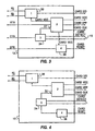
- Figure 3 shows a simplified block diagram of the coupler 12. Signals entering the coupler from the left, as viewed in Fig. 3, correspond to the signals in Figure 2. Signals leaving the coupler 12 on the right, as viewed in Fig. 3, correspond to connections to the Integrated Circuit Card 13 and a card detection switch 15. Circuit means 30 are provided for coupling TX and RX data signals from and to the host processor to CARD I/O.
- a card VCC signal is derived from circuit means 32 which also provides means for enabling a VPP signal and generating and enabling a card clock CARD CLK signal under control of the host processor.
- the circuit represented by block 34 provides means for reporting the presence of a card 13 upon closure of the card detect switch 15 and generating a card present signal CRD PRES applied to the CTS line and circuit 32.
- Circuit means 36 generates a card reset CRD RST signal in response to a data terminal ready signal DTR and card VCC.
- FIG. 4 shows an alternate embodiment of the invention in the case where the card enable control and CARD RESET pulse are generated in the coupler 12 without host processor control.
- Circuit means 30 combines the host processor TX and RX signals with the CARD I/O signal. It is enabled by circuit means 32 which as hereinabove described provides a means of enabling the CARD VCC, CARD VPP, and generating and enabling CARD CLK signals. Circuit 32 is enabled by circuit 34 which responds to the presence of a card and enables circuits 32 and 36. When a card is removed it powers down all card contacts and circuit 36 is arranged to produce a low CARD RESET pulse for a controlled period of time, then presenting a high CARD RESET state until the card is removed.
- the combining means 30 combines the RX and TX signals from the host processor with the I/O lines of both CARD I/O signals.
- each card receives the transmissions of the other card and the host processor, and the host processor receives the transmissions of both cards (assuming they are both present).
- the card clock signal CRD CLK is developed by oscillator 40, comprising a Y1-3.5795 Mhz crystal 41, which is connected across resistors 42 and 43.
- One end of resistor 42 is connected to pin 1 of invertor 44.
- the one end of resistor 42 has also connected thereto one end of capacitor 45, the other end of which is connected to ground.
- the junction of resistors 42 and 43 is connected between the output pin 2 of invertor 44 and the input pin 3 of invertor 46.
- the other end of resistor 43 is connected to one end of capacitor 47, the other end of which is connected to ground.
- Crystal 41, resistors 42, 43, capacitors 45 and 46 and invertor 41, and pins 1 and 2 of invertor 44 form a free running Pierce crystal oscillator circuit which develops a clock signal at the output.
- the output which is taken from pin 2 of invertor 44 is applied to pin 3 of invertor 46 where the clock signal is buffered.
- the output of invertor 46 taken at pin 4 thereof is applied to one input of Nand gate 48.
- the other input of Nand gate 48 receives the CRD ON gate signal when a request to send signal RTS is applied to pin 4 of J2 and the associated invertor J2-5.
- the request to send signal RTS which is applied to pin 4 of U4 is converted to a TTL level and its output taken from pin 5 of U4 and applied to pin 5 of invertor 50.
- the output of invertor 50 taken at pin 6 thereof is applied to one input of Nand gate 51. If pin 2 of Nand gate 51 to which the signal is applied is at a 5 volt DC level and pin 1 has applied thereto a card present CRD PRS signal at a 5 volt DC level, then pin 3 of Nand gate 51 will go to ground.
- a smart card must be inserted in the connector and switch 15 closed before a CRD PRS signal will be available on pin 1 of gate 51 at a 5 vdc level.
- Nand gate 51 is an open drain device, a pull up resistor 52 is connected from the output line of gate 51 to VCC.
- the output of Nand gate 51 is connected to pin 9 of invertor 53, the output of which taken at pin 8 thereof provides the CRD ON signal.
- the CRD ON signal does three things. It is applied to the powered up visual indicator circuit. To this end, CRD ON is applied to pin 13 of invertor 54. Output pin 12 of invertor 54 is connected through current limiting resistor 55 to pin 4 of connector J3. Pin 4 has connected thereto a light emitting diode LED which is returned to VCC via pin 3 of connector J3. Upon insertion of a card into the card connector and consequent closure of switch 15, light emitting diode connected between resistor 55 and VCC provides a visual indication that CRD ON is at a 5dc level. This provides the user with a visual indication that the smart card is powered up. Secondly, the CRD ON signal is applied to pin 5 of Nand gate 48.
- the card clock is applied via series load current limiting resistor 58 to limit the current in case of short circuit.
- Nand gate 48 is an open drain device, a pull up resistor 59 is connected between output pin 6 of Nand gate 48 and CRD VCC so that the pull up is only active when CRD VCC is at a 5 vdc level.
- the third function of the CRD ON signal outputted from invertor 53 is to generate a CRD VCC signal. This is to be distinguished from the VCC voltage developed by regulator 70.
- the CRD ON signal is applied to the CRD VCC circuit comprising transistors 60 and 61, resistors 62, 63 and 64, and voltage regulator 65 CRD resistor 62 has one end connected to the base of transistor 60 and its other end adapted to receive the CRD ON signal.
- the collector of transistor 60 is connected via resistors 63 and 64 to the emitter of transistor 61.
- the junction of resistors 63 and 64 is returned to the base of transistor 61 and its collector is connected to the input of voltage regulator 65, which provides a 5 volt dc regulated output CRD VCC signal applied to pin 6 of J4 and the C1 contact of the integrated circuit card.
- transistor 60 When CRD ON is at ground level, transistor 60 is in its cut off state and the base of transistor 61 is pulled to plus 12 volts dc through resistor 64 connected to a twelve volt source. This puts transistor 61 in cut off, and nothing occurs.
- a CRD ON signal at a 5 volt dc level is applied to the base electrode of transistor 60, base current therein is limited and transistor 60 is put in conduction. In turn, the base of transistor 61 is pulled to ground through series resistor 63 and transistor 61 switched into conduction.
- a 12 volt dc signal appears on the collector of transistor 61 and is applied to the input of voltage regulator 65.
- Voltage regulator 65 regulates the 12 volt dc supply to plus 5 volts dc to establish the CRD VCC signal. This voltage is applied to the smart card and several pull up resistors as hereinbefore described.
- VCC voltage regulator 70 which takes a voltage input from 7 volts dc to 30 volts dc and regulates it to a 5 volt dc.
- the input voltage to regulator 70 may be applied via an external plug in jack J1.
- the VCC source 70 supplies power to other circuits in the coupler but not to the smart card. To this end, VCC is applied to one contact of card on switch 15, the other contact of which is connected to the RC circuit comprising resistors 71 and 72 and capacitor 73. Capacitor 73 is connected at one end to the junction of resistors 71 and 72 and at its other end to the grounded end of resistor 72.
- the junction point 74 provides a card presence signal CRD PRS which is applied to Nand gate 51 and to pin 11 of invertor 75.
- Output pin 10 of invertor 75 is connected to pin 7 of U4 where it is converted to an RS 232 level as the clear to send signal CTS.
- CTS is taken from pin 2 of U4 and connected to the host via the RS 232 cable.
- U4 and capacitors 76, 77, 78 and 79 form an RS 2321 TTL voltage level shifter.
- This level shifter includes 4 invertors 1, 2, 3 and 4 which convert TTL levels at terminals 18, 7, 6 and 19 of U4 to RS 232 levels at terminals 1, 2, 3 and 24 of U4.
- Terminal 2 connects the clear to send signal CTS to the host and terminal 24 applies the receive data signals RS to the host converted to the RS 232 levels through U4 Shifter.
- U4 also includes 3 invertors 5, 6 and 7 which convert RS 232 signals from the host to TTL levels used in the coupler.
- the request to send level RTS is applied to pin 4 of U4 and its corresponding TTL level output taken at pin 5 is applied to input pin 5 of inverter 50.
- a request to send signal RTS from the host computer is applied to pin 4 of U4 and converted to a TTL level.
- the signal is taken at pin 5 U4 and applied to pin 5 of invertor 50.
- the output of invertor 50 taken from pin 6 thereof is applied to one input of Nand gate 51, the other input of which receives a card present CRD PRS signal, If pin 2 of Nand gate 51 is at a 5 volt dc level and pin 1 receives a CRD PRS signal at a 5 volt dc level, then the output of Nand gate 51 will go to ground.
- a smart card must be inserted in the connector before a CRD PRS signal is available.
- a data terminal ready signal DTR from the host computer is applied to pin 16 of U4 and is converted to TTL level. This signal taken at pin 17 of U4 is applied to pin 9 of Nand gate 80.
- the other input of Nand gate 80 receives a VCC signal.
- pin 9 is at 5 volts dc level and the output at pin 8 is maintained at ground through resistor 81 connected to terminal 5 of connector J4. Terminal 5 is in turn connected to contact C2 of the smart card.
- Resistor 81 serves to limit current in case of short circuit.
- Transmit data TX from the host computer is applied to pin 23 and converted to a TTL level.
- the signal taken at pin 22 of U4 is applied to pin 1 of tri-state driver 83 which has its input at pin 2 grounded and its output terminal at pin 3 connected to CRD VCC through resistor 84.
- driver 83 is enabled, i.e., switched and outputs on low signal.
- pin 1 of driver 83 is at 5 volts dc-level
- pin 3 is pulled up if CRD VCC is present and driver 83 acts as an open switch.
- the output of driver 83 is applied through series resistor 85 to the smart card inputoutput terminal 9 of connector J4 and contact C7 of the integrated circuit card.
- driver 83 is also looped back to terminal 19 of U4 and converted to an RS 232 level for application to the host. This provides a loop back path so that any data transmitted into the coupler is echoed to the host computer receive data input. Smart card data and any data sent from the host computer are applied to pin 19 where it is converted to the RS 232 level and to the host computer receive data input.
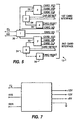
- Figure 7 shows a power supply for the coupler 12 as a means of parasitically supplying +5 volts and ⁇ 12 volts for coupler operation from the EIA-232/V.28 input signals, without destroying the signal integrity of the TX signal.
- a coupler power signal DSR is applied to a voltage regulator 21 which provides ⁇ 12 vdc output for operation of the coupler.
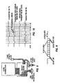
- FIG. 9 there is shown a typical asynchronous character frame on a line with eight data bits, an even parity bit and two stop bits.
- the line is normally in a MARK state, and the beginning of a character is signaled by the transition to a SPACE state for the start bit.
- Each bit occupies one Elementary Time Unit, or ETU.
- the total character occupies twelve ETUs, one for the start bit, eight for the data bits, one for the parity bit, and two for the stop bits.
- Figure 10 shows by means of a timing diagram how internally connecting the transmitted data from the host processor to the card I/O line and the received data line of the host processor is used to detect errors.
- the host processor has transmitted a character to the coupler on the TX terminal.
- the second timing diagram or line shows the character after noise on the line has corrupted the character and inverted a bit. This is indicated as a transmission error identified by the arrow.
- This data is received by the portable card and tested for even parity. Due to the transmission error, the parity test fails and the card issues an error signal on the I/O line from 10.5 to 11.5 ETUs after the leading edge of the start bit as shown in the third timing diagram.
- the fourth timing diagram shows the character as received by the host processor.
- the host processor detects that the character may have been received in error by the card because the received character has bad parity, the received character does not match exactly the transmitted character, and the received character generates a FRAMING ERROR since it has a SPACE during the period of the two stop bits.
- a clear to send CTS signal is sent to the host which in turn generates a data terminal ready signal DTS that results in application of a reset CRD RST signal to the portable data card.
- terminal 9 of J4 is pulled up to CRD VCC through resistors 84 and 85, a loopback test for communication errors can only be performed if there is a request to send (RTS) input signal applied to J4 and a card is present in the card connector or reader.
- RTS request to send
Abstract
Description
- The invention relates to a method and coupler for serial communication between a Universal Asynchronous Receiver Transmitter terminal (UART) such as, would be associated, for example, with a host processor, a personal computer, or point of sale device or the like and a portable data carrier.
- A portable data carrier is a portable device which contains integrated circuit(s). Examples of portable data carriers are Integrated Circuit Cards, data keys, smart cards, and smart coins. Recent advances in the manufacture of integrated circuit chips have led to the development of a multipurpose plastic card having a microprocessor no bigger than a penny embedded therein known as a "smart card". Such cards and their method of manufacture and methods for transmitting signals between the cards and the host terminal are well known.
- Because of the built-in computer logic and memory, the so called "smart card" has found use in a variety of applications. The "smart card" can be used for encoding confidential data, as an electronic security key for protecting information and property, a portable file for monitoring medical or insurance records, payroll records, funds transfers and inventory controls, to name a few.
- Despite the popularity of portable data carriers containing integrated circuits such as, for example, the so-called "smart cards", heretofore it has been thought necessary when coupling such devices serially to a host terminal that the coupler or smart card reader must contain a microprocessor and that "bit banging" of the input and output signals was the only way to process the input and output. In such arrangements, the microprocessor in addition to processing the input/output signals is also responsible for developing the major control and interface signals to enable communication.
- Couplers for Integrated Circuit Cards interface to host processors or terminals, simply referred to as hosts, using a number of different serial I/O channels and communication protocols. Commands from the host are transmitted to the coupler over the serial I/O channel as a series of bytes. Handshake lines of the serial I/O channel are sometimes used by the host, but only to control the flow of commands to the coupler, not to control the coupler/card interface. The presence of an Integrated Circuit Card in the coupler is sometimes reported to the host using a serial I/O channel handshake line.
- All couplers available today contain a processor, such as an 8051, which controls the card interface and accepts commands from the host. Because the microprocessor receives characters from the host processor and retransmits them to the Integrated circuit Card, a performance penalty is imposed. A major penalty or disadvantage of such couplers is that the microprocessor in the coupler interface slows down the process of interfacing the smart card to the host terminal. This is due to the fact that for transmissions from the host terminal, the microprocessor has to "listen" for a command from the host terminal and then interpret and reformat the command before sending it to the smart card. The same would be true when the smart card transmits a message to the host terminal. The microprocessor has to receive the message, reformat the message and then transit the reformatted message directly. A system which can avoid the use of a microprocessor would process information two-to-three times faster.
- Another disadvantage of known systems is the cost resulting from the necessity of incorporating a microprocessor in the coupler. A system which avoids the use of a microprocessor would provide a substantial cost benefit.
- U.S. Pat. No. 4,767,918 describes a reading and writing apparatus for portable recording medium. A clock oscillator is incorporated in the apparatus and the clock signal is selectively supplied to the medium via an AND gate in response to a binary logic signal supply voltage for the reading and writing apparatus. An external control unit may also provide a clock-enable signal. A medium present signal is generated upon insertion of a portable recording medium in a contact section and, in response to said medium present signal, a card voltage to be applied to the portable recording medium is generated.
- Accordingly, it is a primary object of the present invention to provide a coupler as an interface between a portable data carrier and a host information processing terminal which avoids the use of a microprocessor.
- Another object of the present invention is to provide a coupler as an interface between a portable data carrier and host processor including a means of communicating with the portable data carrier over a serial I/O communications channel without the coupler receiving and retransmitting characters communicated between the portable data carrier and the host processor.
- A further object of the present invention is to provide a coupler as an interface between a portable data carrier and host processor which controls portable data carrier interface signals using handshake lines of a serial I/O communications channel.
- Yet another object of the present invention is to provide a coupler as an interface between a portable data carrier and a host processor wherein said coupler is powered with electrical power parasitically derived from a serial I/O communications channel.
- Still another object of the present invention is to provide a coupler as an interface between a portable data carrier and a host processor which includes a means of enabling required electrical signals when the portable data carrier's presence is detected.
- A further object of the present invention is to provide a coupler as an interface between a portable data carrier and a host processor which provides sequences of electrical signals such as RESET signals when a portable data carrier's presence is detected.
- Another object of the present invention is to provide a coupler as an interface between a portable data carrier and a host processor in which received and transmitted data from the host processor is connected with data transmitted by the portable data carrier to allow detection of error signals generated by the portable data carrier.
- Still another object of the present invention is to provide a coupler as an interface between a portable data carrier and a host processor which includes a means of connecting received data from the host and data transmitted from the host processor with data transmitted by the portable data carrier to allow the host processor to receive its own transmissions and detect errors in communication.
- A further object of the present invention is to provide a coupler as an interface between a portable data carrier and a host processor which includes a connecting means which replaces the conventional interface driver and receiver integrated circuit(s) of a host processor communications device.
- A still further object of the present invention is to provide a device for interfacing one or more portable data carriers by which the communications of each portable data carrier and a local or host processor are combined with the communications of each other portable data carrier or local or remote processor, such transmissions being receivable by the other portable data carriers and local or host processors, if any.
- Yet another object of the present invention is to provide a low cost solid state coupler as an interface between a portable data carrier and a host processor which avoids the use of a microprocessor in the coupler and retransmission of characters communicated between the portable data carrier and the host processor.
- In accordance with a preferred embodiment of the invention, a coupler for interfacing a portable data carrier with a host processor comprises first terminal means (U4-23) adapted to receive data from the host processor, input/output terminal means (J4-9) adapted to receive input data from the data carrier and the data received at the first terminal means from the host processor, second terminal means (U4-19) connected to said input/output terminal means to enable the input data from said data carrier to be translated to the host processor and control means (83) connected between said first and said second terminal means and said input/output terminal means for translating input data from said first terminal means to said second terminal means and to the input/output terminal means.
- In accordance with this embodiment, input data is looped back between the first and the second terminal means and the control means (83) comprises switching means for switching data to the second terminal means and the input/output terminal means.
- Card connector means may be provided for receiving the portable data carrier along with means for controlling its switching means for applying a bias voltage to said control means in response to insertion of said data carrier into said connector means.
- In a further variation of the system, means are provided for receiving data from the host processor and translating said data to the input/output terminal means adapted to be connected to said data carrier and simultaneously echoing the data received to the host processor.
- The system further includes means for connecting data from the portable data carrier to the input/output data terminal means and means responsive to the connection of said data carrier to the input/output terminal means for generating control signals to enable translation of data from the data carrier to the host processor and data from the host processor to the data carrier. Feedback means assures echoing the data received from the host processor back to the host processor to allow said host processor to receive its own transmission.
- The invention also relates to a method for interfacing a portable data carrier with a host processor via a signal coupler comprising the steps of generating a carrier present signal CRD PRS and a clear to send signal CTS upon insertion of a portable data carrier in a connector adapted to receive said carrier; generating a CRD ON signal in response to a request to send signal from said host processor after receipt by the host processor of a clear to send signal; generating a card voltage signal CRD VCC to be applied to the portable data carrier in response to said CRD ON signal and transmitting and receiving data between said host processor and portable data carrier, said step of transmitting and receiving data including the step of echoing data from the host processor to allow said host processor to receive its own transmission for detecting errors in communication.
- A further variation of the method further includes generating a clock signal CRD CLK in the coupler and applying the clock signal to the data carrier.
- According to the inventive method, the received and transmitted characters of the data to detect multiple bit errors are compared and retransmission of characters transmitted by the data carrier is ordered upon detection of an error.
- In accordance with a specific arrangement of the present invention, the coupler is connected to a host processor via an EIA-232/V.28 serial I/O channel which provides Clear-To-Send (CTS), Request-To-Send (RTS), Data-Set-Ready (DSR) and Data-Terminal-Ready (DTR) signals as well as Transmit-Data (TX) and Receive-Data (RX). The host will include a universal asynchronous receiver transmitter (UART) which may be hardware or software and is assumed to be a Data Terminal Equipment (DTE) device, while the coupler acts as a Data-Communications-Equipment (DCE) device. Other forms of serial link such as RS-422 and Integrated Services Digital Network (ISDN) protocols can also be used.
- The coupler provides a means of coupling the TX and RX lines to the I/O line of the Integrated Circuit Card. Feedback means may be provided between the TX and RX lines to be used for error detection. In full duplex Integrated Circuit Cards, the TX and RX lines are connected to the corresponding Integrated Circuit Card contacts of the Integrated Circuit Cards. Of course, contactless interfaces are also possible.
- In accordance with the present invention, circuit means is provided which detects the presence of an Integrated Circuit Card in the coupler's card connector. A further circuit means is provided to couple this signal to the card present CTS line of the EIA-232/V.28 link to provide card present CTS signals to the host indicating that a card is present in the coupler. The host commands the coupler to raise or lower the card's RESET line by asserting or clearing the DTR signal, while the coupler provides means for controlling the RESET line in response to the state of the DTR signals. The RESET line is qualified with CARD VCC.
- The RTS signal is used by the host observer to request the CARD VCC be raised or lowered. The Coupler provides a means of controlling CARD VCC in response to the RTS signal. In addition, the coupler may qualify this signal with the presence of a card in the connector. The coupler further provides a means of enabling a clock signal to the CARD CLK contact of the Integrated Circuit Card when RTS is active. The coupler further provides a means of enabling CARD VPP when RTS is active. Thus RTS controls CARD VCC, CARD VPP and CARD CLK.
- The coupler can provide a means of controlling DSR to reflect the status of coupler power. This is used as a diagnostic tool to detect the presence of a working coupler.
- CARD CLK, CARD VCC, and CARD VPP can be controlled independently using additional handshake lines. In addition, the coupler can include a means of providing a suitable RESET pulse when RTS requests that CARD VCC be raised to a card.
- Further, the CARD VCC, CARD CLK and CARD RESET may all be provided by the coupler when a card is inserted. This embodiment has particular application in access control applications where the coupler communicates with a host processor via a current loop interface. In this case no handshake lines need to be run to the access control portal. The presence of a card is signaled to the host processor by the card's Answer-To-Reset.
- Power to the coupler can be provided by an external supply, a battery, a connection in common to the EIA-232/V.28 channel, or by parasitically removing power from the EIA-232/V.28 channel. The latter has the advantage of simplicity and low cost but restricts the coupler to low power Integrated Circuit Cards. Other types of serial I/O channels can also be tapped for power.
- Power and the required EIA-232/V.28 signals can be provided to the coupler if a cable which connects the coupler to the host processor is terminated such that it connects directly to a socket (or sockets) which normally house the EIA-232/V.28 driver and receiver integrated circuit(s). In this case the signal levels are typically TTL, not EIA-232/V.28 and power is directly available. This provides a very low cost option as it reduces the circuitry in both the host and coupler for level conversion, and alleviates the need for a special power supply. This is the preferred approach for couplers which are added within the housing of an existing host processor, such as within the disk drive bay of a PC.
- ISO has standardized a communication protocol for integrated circuit cards which uses a unique byte retransmission request bit (UGON ++++). A retransmission bit is sent by the receiver of a character when the character has been received in error. The transmitter then retransmits the erroneous character. The protocol is designed to be incompatible with a standard Universal Asynchronous Receiver Transmitter as is used on most asynchronous I/O channels today. The retransmission bit must be transmitted during what is normally the stop bit of the transmitted character. A normal Universal Asynchronous Receiver Transmitter (UART) may see this as a start bit, but would not report it to the host until a full 12 Elementary Time Units (ETUs) of character time has elapsed. The transmitter may well be into the transmission of a new character before the error report is detected, resulting in a communications collision.
- In accordance with a particular object and advantageous feature of the present invention, there is provided feedback within the coupler between the TX and RX EIA-232/V.28 lines. This allows the host to receive it's own transmissions. If the card signals that a retransmission is requested, then the UART reports a framing error as the retransmission bit is within the normal stop bit of the character is question. In addition, if a double bit error is produced on the line and the Integrated Circuit card does not detect the error the host can still detect the error by comparing the received and transmitted characters. This provides a robust means of error detection for the host. In the case of errors in characters transmitted by the card, the host can detect these using the parity bit, and once an error has been detected in a transmission the entire command can be repeated to ensure valid data. Once a transmission protocol which includes block error detecting codes, error detection and correction becomes more conventional with retransmission at the block level.
- Multiple cards can be connected together to share a single serial I/O channel. In this case, each card can receive the transmissions of any other cards on the channel as well as any host processor(s) or local processor(s) on the channel (if any). A host processor (or processors) or local processor (or processors) on the channel can receive the transmissions of any cards or other processors on the channel. Collisions on the communications channel are resolved by an appropriate Integrated Circuit Card communications protocol, or additional handshake lines.
- These and other objects and advantages of the invention will become readily apparent to those skilled in the art from the detailed description of the preferred embodiments to be considered in connection with the following drawings, wherein like reference characters represent like parts throughout the several views.
- Figure 1 shows a typical system configuration of the present invention in block diagram form.
- Figure 2 shows a typical UART configuration within a host processor for serial I/O communications with EIA-232/V.28 level conversion.
- Figure 3 shows a block diagram of the coupler in accordance with the present invention.
- Figure 4 shows a block diagram of the coupler in accordance with the present invention in the case where the card enables and CARD RESET pulse are generated in the coupler without host processor control.
- Figure 5 shows a block diagram of the coupler in accordance with the present invention in the case where there are two Integrated Circuit Card Interfaces on the one coupler.
- Figure 6 is a schematic diagram of the coupler in accordance with the present invention.
- Figure 7 shows a power supply for the coupler which in accordance with the present invention parasitically supplies +5 volts and ±12 volts (typical) for coupler operation from the EIA-232/V.28 input signals, without destroying the signal integrity of the TX signal.
- Figure 8 shows a typical layout of the card connector circuit board and cable connectors for the present invention.
- Figure 9 shows a typical asynchronous character frame as used in the present invention, and
- Figure 10 is a timing diagram of a transmitted character illustrating how internally connecting the transmitted data from the host processor to the card I/O line and the received data line of the host processor is used to detect errors.
-
- Figure 1 shows a typical system configuration with a personal computer acting as a host processor, 10, an EIA-232/V.28 serial communication line comprising an RS 232
cable 11 acting as a serial I/O channel,coupler 12, and an Integrated Circuit Card, (ICC) 13, acting as the portable data carrier.ICC 13 is a plastic card containing amicro processor 14 positioned on the card in accordance with ISO nomenclature specification 7816.ICC 13 includes contacts C1-C8 each of which is reserved in accordance with ISO 7816 standard for a particular signal. For example, card contact C1 receives a 5Vdc card VCC voltage (CRD VCC), contact C2 receives the card reset signal (CRD RST), contact C3 receives the card clock signal (CRD CLK). Card input and output data are received and sent via card contact C7. Contacts C1-C8 are connected within the coupler to contact terminals of a card connector J4. Card Connector J4 includes a switch 15 (shown in Fig. 6) conveniently positioned to be actuated to a closed position upon insertion of the card so as to provide a card present (CRD PRS) signal to thehost processor 10. Communication with the host processor is maintained via a RS 232serial communication line 11 connected to thehost processor 10 which may be any type of terminal adapted for serial communication and usually containing a UART which may be either hardware or software. As shown in Fig. 1,host 10 may be a personal computer including adisplay 16,data input keyboard 17 andprocessor 18. - Figure 2 shows a typical (UART) 20 configuration within
host processor 10. The 8250 UART is common in many personal computers and is the UART which corresponds to the software listings included in the 8250 Universal Asynchronous Receiver Transmitter. The UART 20 provides and receives typical serial I/O communications channel signals, including a transmit data to card signal TX, a receive data from card signal RX, a card present signal CTS, an enable card VCC and CLK signal RTS, a reset card signal DTR and a coupler power OK signal WSR. The latter signal is optional. The sense of the control signals are as follows:Card Present CTS = 0 Vcc ON RTS = 0 Card Reset DTR = 1 Coupler Active DSR = 0 - The signals at the UART are at RS 232 levels and converted through integrated circuit board U4 to TTL levels. Circuit board U4 may be a
MAX 236 available from Maximum Semiconductor and includes a plurality of invertors connected as shown to ensure the proper sense and line of the signals as shown in Fig. 2. - Figure 3 shows a simplified block diagram of the
coupler 12. Signals entering the coupler from the left, as viewed in Fig. 3, correspond to the signals in Figure 2. Signals leaving thecoupler 12 on the right, as viewed in Fig. 3, correspond to connections to theIntegrated Circuit Card 13 and acard detection switch 15. Circuit means 30 are provided for coupling TX and RX data signals from and to the host processor to CARD I/O. - A card VCC signal is derived from circuit means 32 which also provides means for enabling a VPP signal and generating and enabling a card clock CARD CLK signal under control of the host processor. The circuit represented by
block 34 provides means for reporting the presence of acard 13 upon closure of the card detectswitch 15 and generating a card present signal CRD PRES applied to the CTS line andcircuit 32. Circuit means 36 generates a card reset CRD RST signal in response to a data terminal ready signal DTR and card VCC. - Figure 4 shows an alternate embodiment of the invention in the case where the card enable control and CARD RESET pulse are generated in the
coupler 12 without host processor control. Circuit means 30 combines the host processor TX and RX signals with the CARD I/O signal. It is enabled by circuit means 32 which as hereinabove described provides a means of enabling the CARD VCC, CARD VPP, and generating and enabling CARD CLK signals.Circuit 32 is enabled bycircuit 34 which responds to the presence of a card and enablescircuits circuit 36 is arranged to produce a low CARD RESET pulse for a controlled period of time, then presenting a high CARD RESET state until the card is removed. - Referring to Figure 5, there is shown a block diagram of the
coupler 12 in the case where there are a first and a second Integrated Circuit Card Interfaces on one coupler. In this case, the combining means 30 combines the RX and TX signals from the host processor with the I/O lines of both CARD I/O signals. In this case, each card receives the transmissions of the other card and the host processor, and the host processor receives the transmissions of both cards (assuming they are both present). - Referring to Figure 6, there is illustrated a detailed schematic of the present invention. The card clock signal CRD CLK is developed by oscillator 40, comprising a Y1-3.5795
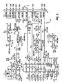
Mhz crystal 41, which is connected acrossresistors resistor 42 is connected to pin 1 ofinvertor 44. The one end ofresistor 42 has also connected thereto one end of capacitor 45, the other end of which is connected to ground. The junction ofresistors output pin 2 ofinvertor 44 and theinput pin 3 ofinvertor 46. The other end ofresistor 43 is connected to one end ofcapacitor 47, the other end of which is connected to ground.Crystal 41,resistors capacitors 45 and 46 andinvertor 41, and pins 1 and 2 ofinvertor 44 form a free running Pierce crystal oscillator circuit which develops a clock signal at the output. The output which is taken frompin 2 ofinvertor 44 is applied to pin 3 ofinvertor 46 where the clock signal is buffered. The output ofinvertor 46 taken atpin 4 thereof is applied to one input ofNand gate 48. The other input ofNand gate 48 receives the CRD ON gate signal when a request to send signal RTS is applied to pin 4 of J2 and the associated invertor J2-5. - The request to send signal RTS which is applied to pin 4 of U4 is converted to a TTL level and its output taken from
pin 5 of U4 and applied to pin 5 ofinvertor 50. The output ofinvertor 50 taken atpin 6 thereof is applied to one input ofNand gate 51. Ifpin 2 ofNand gate 51 to which the signal is applied is at a 5 volt DC level andpin 1 has applied thereto a card present CRD PRS signal at a 5 volt DC level, then pin 3 ofNand gate 51 will go to ground. A smart card must be inserted in the connector and switch 15 closed before a CRD PRS signal will be available onpin 1 ofgate 51 at a 5 vdc level. BecauseNand gate 51 is an open drain device, a pull upresistor 52 is connected from the output line ofgate 51 to VCC. The output ofNand gate 51 is connected to pin 9 ofinvertor 53, the output of which taken atpin 8 thereof provides the CRD ON signal. - The CRD ON signal does three things. It is applied to the powered up visual indicator circuit. To this end, CRD ON is applied to pin 13 of
invertor 54.Output pin 12 ofinvertor 54 is connected through current limitingresistor 55 to pin 4 of connector J3.Pin 4 has connected thereto a light emitting diode LED which is returned to VCC viapin 3 of connector J3. Upon insertion of a card into the card connector and consequent closure ofswitch 15, light emitting diode connected betweenresistor 55 and VCC provides a visual indication that CRD ON is at a 5dc level. This provides the user with a visual indication that the smart card is powered up. Secondly, the CRD ON signal is applied to pin 5 ofNand gate 48. This switches the gate ON to provide a card clock output signal CRD CLK atline 57. The card clock is applied via series load current limitingresistor 58 to limit the current in case of short circuit. BecauseNand gate 48 is an open drain device, a pull upresistor 59 is connected betweenoutput pin 6 ofNand gate 48 and CRD VCC so that the pull up is only active when CRD VCC is at a 5 vdc level. The third function of the CRD ON signal outputted frominvertor 53 is to generate a CRD VCC signal. This is to be distinguished from the VCC voltage developed by regulator 70. - To this end, the CRD ON signal is applied to the CRD VCC
circuit comprising transistors resistors CRD resistor 62 has one end connected to the base oftransistor 60 and its other end adapted to receive the CRD ON signal. The collector oftransistor 60 is connected viaresistors 63 and 64 to the emitter oftransistor 61. The junction ofresistors 63 and 64 is returned to the base oftransistor 61 and its collector is connected to the input of voltage regulator 65, which provides a 5 volt dc regulated output CRD VCC signal applied to pin 6 of J4 and the C1 contact of the integrated circuit card. - When CRD ON is at ground level,
transistor 60 is in its cut off state and the base oftransistor 61 is pulled to plus 12 volts dc throughresistor 64 connected to a twelve volt source. This putstransistor 61 in cut off, and nothing occurs. When a CRD ON signal at a 5 volt dc level is applied to the base electrode oftransistor 60, base current therein is limited andtransistor 60 is put in conduction. In turn, the base oftransistor 61 is pulled to ground through series resistor 63 andtransistor 61 switched into conduction. A 12 volt dc signal appears on the collector oftransistor 61 and is applied to the input of voltage regulator 65. Voltage regulator 65 regulates the 12 volt dc supply to plus 5 volts dc to establish the CRD VCC signal. This voltage is applied to the smart card and several pull up resistors as hereinbefore described. - Power to the circuits is supplied through voltage regulator 70 which takes a voltage input from 7 volts dc to 30 volts dc and regulates it to a 5 volt dc. The input voltage to regulator 70 may be applied via an external plug in jack J1. The VCC source 70 supplies power to other circuits in the coupler but not to the smart card. To this end, VCC is applied to one contact of card on
switch 15, the other contact of which is connected to the RCcircuit comprising resistors 71 and 72 and capacitor 73. Capacitor 73 is connected at one end to the junction ofresistors 71 and 72 and at its other end to the grounded end of resistor 72. Whenswitch 15 is closed, due to the presence of a card in the connector, the junction point 74 provides a card presence signal CRD PRS which is applied toNand gate 51 and to pin 11 ofinvertor 75.Output pin 10 ofinvertor 75 is connected to pin 7 of U4 where it is converted to an RS 232 level as the clear to send signal CTS. CTS is taken frompin 2 of U4 and connected to the host via the RS 232 cable. When the smart card is withdrawn from the card connector, the CRD PRS line is pulled to ground by resistor 72. - U4 and
capacitors invertors terminals terminals invertors pin 5 is applied to inputpin 5 ofinverter 50. - A request to send signal RTS from the host computer is applied to pin 4 of U4 and converted to a TTL level. The signal is taken at
pin 5 U4 and applied to pin 5 ofinvertor 50. The output ofinvertor 50 taken frompin 6 thereof is applied to one input ofNand gate 51, the other input of which receives a card present CRD PRS signal, Ifpin 2 ofNand gate 51 is at a 5 volt dc level andpin 1 receives a CRD PRS signal at a 5 volt dc level, then the output ofNand gate 51 will go to ground. A smart card must be inserted in the connector before a CRD PRS signal is available. - A data terminal ready signal DTR from the host computer is applied to pin 16 of U4 and is converted to TTL level. This signal taken at
pin 17 of U4 is applied to pin 9 ofNand gate 80. The other input ofNand gate 80 receives a VCC signal. Upon the presence of a DTR signal,pin 9 is at 5 volts dc level and the output atpin 8 is maintained at ground throughresistor 81 connected toterminal 5 of connector J4. Terminal 5 is in turn connected to contact C2 of the smart card.Resistor 81 serves to limit current in case of short circuit. Whenpin 9 ofNand gate 80 is at ground level, no output appears atpin 8 and the CRD RST line is pulled up by resistor 82 if the CRD VCC voltage is turned on. - Transmit data TX from the host computer is applied to pin 23 and converted to a TTL level. The signal taken at
pin 22 of U4 is applied to pin 1 oftri-state driver 83 which has its input atpin 2 grounded and its output terminal atpin 3 connected to CRD VCC through resistor 84. When terminal 22 andpin 1 ofdriver 83 are low, i.e., at ground level,driver 83 is enabled, i.e., switched and outputs on low signal. Whenpin 1 ofdriver 83 is at 5 volts dc-level,pin 3 is pulled up if CRD VCC is present anddriver 83 acts as an open switch. The output ofdriver 83 is applied throughseries resistor 85 to the smartcard inputoutput terminal 9 of connector J4 and contact C7 of the integrated circuit card. The output ofdriver 83 is also looped back toterminal 19 of U4 and converted to an RS 232 level for application to the host. This provides a loop back path so that any data transmitted into the coupler is echoed to the host computer receive data input. Smart card data and any data sent from the host computer are applied to pin 19 where it is converted to the RS 232 level and to the host computer receive data input. - Figure 7 shows a power supply for the
coupler 12 as a means of parasitically supplying +5 volts and ±12 volts for coupler operation from the EIA-232/V.28 input signals, without destroying the signal integrity of the TX signal. To this end, in addition to transmit data TX and a request to send signal RTS from the host, a coupler power signal DSR is applied to avoltage regulator 21 which provides ±12 vdc output for operation of the coupler. - Referring now to Figure 9, there is shown a typical asynchronous character frame on a line with eight data bits, an even parity bit and two stop bits. The line is normally in a MARK state, and the beginning of a character is signaled by the transition to a SPACE state for the start bit. Each bit occupies one Elementary Time Unit, or ETU. The total character occupies twelve ETUs, one for the start bit, eight for the data bits, one for the parity bit, and two for the stop bits.
- Figure 10 shows by means of a timing diagram how internally connecting the transmitted data from the host processor to the card I/O line and the received data line of the host processor is used to detect errors. In the first timing diagram, at the topmost line of the figure, the host processor has transmitted a character to the coupler on the TX terminal. The second timing diagram or line shows the character after noise on the line has corrupted the character and inverted a bit. This is indicated as a transmission error identified by the arrow. This data is received by the portable card and tested for even parity. Due to the transmission error, the parity test fails and the card issues an error signal on the I/O line from 10.5 to 11.5 ETUs after the leading edge of the start bit as shown in the third timing diagram. The fourth timing diagram shows the character as received by the host processor. The host processor detects that the character may have been received in error by the card because the received character has bad parity, the received character does not match exactly the transmitted character, and the received character generates a FRAMING ERROR since it has a SPACE during the period of the two stop bits. Upon insertion of a card into the card connector, a clear to send CTS signal is sent to the host which in turn generates a data terminal ready signal DTS that results in application of a reset CRD RST signal to the portable data card. Inasmuch as the input/output line of the data card,
terminal 9 of J4 is pulled up to CRD VCC throughresistors 84 and 85, a loopback test for communication errors can only be performed if there is a request to send (RTS) input signal applied to J4 and a card is present in the card connector or reader. - While the invention has been described in connection with certain preferred embodiments, it will be apparent to those skilled in the art that variations will suggest themselves without departing from the scope of the invention. Accordingly, it is intended by the appended claims to cover all such variations and resort should be made to the appended claims to determine the scope of the invention.
Claims (18)
- A coupler (12) for interfacing a portable data carrier (13) with an asynchronous receiver transmitter for asynchronous data transmission (10) comprising:first terminal means (U4-23) adapted to receive asynchronous data transmitted from the asynchronous receiver transmitter,connector means adapted to receive a portable data carrier (13),input/output terminal means (J4-9) adapted to receive:asynchronous input data from the data carrier (13), andthe asynchronous data received at the first terminal means (U4-23) from the asynchronous receiver transmitter (10),second terminal means (U4-19) connected to said input/output terminal means to enable the input data from said data carrier to be translated to the asynchronous receiver transmitter (10), andcontrol means (83) connected between said first (U4-23) and said second (U4-19) terminal means and said input/output terminal means (J4-9) for:translating input data from said first terminal means (U4-23) to said second terminal means (U4-19),translating input data from said first terminal means (U4-23) to the input/output terminal means (J4-9), andgenerating a framing error signal when a character of the asynchronous data received contains an error, said framing error signal being acted upon prior to the transmission of the next character.
- A coupler as set forth in claim 1 including means for looping back said input data (1) between said first (U4-23) and said second (U4-19) terminal means and said control means (83) comprises switching means (83) for switching data to said second terminal means (U4-19) and said input/output terminal means (J4-9).
- A coupler as set forth in claim 2 including card connector means for receiving the portable data carrier and means for controlling said switching means for applying a bias voltage to said control means in response to insertion of said data carrier into said connector means.
- A coupler as set forth in claim 3 further including means for receiving data from the asynchronous receiver transmitter and translating said data to the input/output terminal means adapted to be connected to said data carrier and simultaneously echoing the data received to the asynchronous receiver transmitter.
- A coupler for interfacing a portable data carrier with an asynchronous receiver transmitter as set forth in claim 4, further including means for translating data from the portable data carrier to the input/output data terminal means and means responsive to the connection of said data carrier to the input/output terminal means for generating control signals to enable translation of data from the data carrier to the asynchronous receiver transmitter and data from the asynchronous receiver transmitter to the data carrier.
- A coupler as set forth in claim 5, further including feedback means for echoing the data received from the asynchronous receiver transmitter back to the host processor to allow said asynchronous receiver transmitter to receive its own transmission.
- A coupler as set forth in claim 1, wherein said control means is responsive to insertion of the data carrier into the connector means for enabling input data from the receiver transmitter to be translated to the data carrier and simultaneously looping said input data to said second terminal means to allow for detection of errors in communication.
- A coupler as set forth in claim 7, further including a connector for receiving the data carrier and operatively connecting the data carrier to the first, the second and the input/output terminal means for detecting the presence of a portable data carrier.
- A coupler as set forth in claim 8, further including feedback means allowing the receiver transmitter to receive its own transmission for detecting errors in communication between the receiver transmitter and data carrier.
- A coupler as set forth in claim 1, further including means for parasitically supplying operating voltage levels for coupler operation from the data received from the receiver transmitter without destroying the signal integrity of the data received.
- A coupler as set forth in claim 1, further including means for interfacing multiple portable data carriers with the receiver transmitter by which communications of each portable data carrier and the receiver transmitter are combined with the communications of each other portable data carrier.
- A coupler as set forth in claim 1, wherein said framing error signal is a single bit.
- A coupler as set forth in claim 1, further including means for comparing received and transmitted characters to detect multiple bit errors.
- A method for interfacing a portable data carrier (13) with an asynchronous receiver transmitter (10) for asynchronous data transmission via a signal coupler (12) adapted to receive the portable data carrier (13) in an associated connector comprising:generating a carrier present signal CRD PRS and a clear to send signal CTS upon insertion of the portable data carrier in the connector adapted to receive said carrier; generating a request-to-send RTS signal from said asynchronous receiver transmitter after receipt by the asynchronous receiver transmitter of a clear to send CTS signal;generating a card on CRD ON signal in response to the request to send RTS signal from said receiver transmitter;generating a card voltage signal CRD VCC to be applied to the portable data carrier in response to said CRD ON signal; andtransmitting and receiving data between said receiver transmitter and portable data carrier in response to said generated signals and insertion of a data carrier into the connector, said step of transmitting and receiving data including:a step using first terminal means (U4-23) of the coupler (12) for receiving asynchronous data transmitted from the asynchronous receiver transmitter,a step using input/output terminal means (J4-9) of the coupler for receiving asynchronous input data from the data carrier (13) and the asynchronous data received at the first terminal means (U4-23) from the asynchronous receiver transmitter (10),a step using second terminal means (U4-19) connected to said input/output terminal means for translating the input data from said data carrier to the asynchronous receiver transmitter (10),a step using control means (83) connected between said first (U4-23) and said second (U4-19) terminal means and said input/output terminal means (J4-9) for translating input data from said first terminal means (U4-23) to said second terminal means (U4-19) and to the input/output terminal means (J4-9), anda step using said control means (83) for echoing data from the receiver transmitter to allow said receiver transmitter (10) to receive its own transmission and detect errors in communication on a character by character basis and allow a character error to be acted upon prior to the transmission of the next character.
- A method as set forth in claim 14 further including generating a clock signal CRD CLK in the coupler and applying the clock signal to the data carrier.
- A method as set forth in claim 15, further including comparing the received and transmitted characters of the data to detect multiple bit errors.
- A method as set forth in claim 16, further including ordering retransmission of characters transmitted by the data carrier upon detection of an error.
- A method as set forth in claim 17, further including means for detecting a retransmission signal.
Applications Claiming Priority (2)
| Application Number | Priority Date | Filing Date | Title |
|---|---|---|---|
| US07/548,414 US5149945A (en) | 1990-07-05 | 1990-07-05 | Method and coupler for interfacing a portable data carrier with a host processor |
| US548414 | 1990-07-05 |
Publications (3)
| Publication Number | Publication Date |
|---|---|
| EP0537287A1 EP0537287A1 (en) | 1993-04-21 |
| EP0537287A4 EP0537287A4 (en) | 1996-08-14 |
| EP0537287B1 true EP0537287B1 (en) | 2005-10-26 |
Family
ID=24188764
Family Applications (1)
| Application Number | Title | Priority Date | Filing Date |
|---|---|---|---|
| EP91913849A Expired - Lifetime EP0537287B1 (en) | 1990-07-05 | 1991-04-29 | Method and coupler for interfacing a portable data carrier with a host processor |
Country Status (9)
| Country | Link |
|---|---|
| US (1) | US5149945A (en) |
| EP (1) | EP0537287B1 (en) |
| JP (1) | JP3357048B2 (en) |
| AU (1) | AU8291791A (en) |
| CA (1) | CA2046155C (en) |
| DE (1) | DE69133489T2 (en) |
| IL (1) | IL98077A (en) |
| WO (1) | WO1992001259A1 (en) |
| ZA (1) | ZA913459B (en) |
Families Citing this family (65)
| Publication number | Priority date | Publication date | Assignee | Title |
|---|---|---|---|---|
| US5478995A (en) * | 1986-10-23 | 1995-12-26 | Skidata Computer Gesellschaft M.B.H. | Data carrier with disc shaped carrier structure |
| US5339239A (en) * | 1989-10-13 | 1994-08-16 | Mitsubishi Plastics Industries Limited | Information collecting and/or service furnishing systems by which a user can request information from a central data base using a portable personal terminal and an access terminal |
| FR2654232A1 (en) * | 1989-11-07 | 1991-05-10 | Europ Rech Electr Lab | CONTINUOUS VOLTAGE GENERATOR FOR SUPPLYING AN INTEGRATED CIRCUIT BOARD. |
| FR2675924B1 (en) * | 1991-04-25 | 1993-12-24 | Innovatron Sa | SYSTEM FOR EXCHANGING DATA BETWEEN AN ELECTRONIC OBJECT COUPLED TO A DISTINCT DATA-TRANSFER DEVICE, INSERABLE OBJECT AND CORRESPONDING TRANSFER DEVICE. |
| JPH04329415A (en) * | 1991-04-30 | 1992-11-18 | Fujitsu Ltd | Card type input/output interface device |
| DE4132720A1 (en) * | 1991-10-01 | 1993-04-08 | Gao Ges Automation Org | CHIP CARD AND METHOD FOR THE PRODUCTION THEREOF |
| US5428210A (en) * | 1992-01-10 | 1995-06-27 | National Bancard Corporation | Data card terminal with embossed character reader and signature capture |
| FR2689997B1 (en) * | 1992-04-08 | 1997-06-13 | Innovatron Sa | CONTACTLESS DATA EXCHANGE SYSTEM BETWEEN A TERMINAL AND A MODULAR PORTABLE ASSEMBLY. |
| JPH06177940A (en) * | 1992-12-08 | 1994-06-24 | Mitsubishi Electric Corp | Uart and system using thereof |
| EP0624851A1 (en) * | 1993-05-13 | 1994-11-17 | Angewandte Digital Elektronik GmbH | Coupler between the applications on the card level and the applications on the system level |
| US5450491A (en) * | 1993-08-26 | 1995-09-12 | At&T Corp. | Authenticator card and system |
| US5790885A (en) * | 1993-09-10 | 1998-08-04 | Oki Electric Industry Co., Ltd. | Method for controlling IC card reader/writer to transmit same character frame upon receiving echo back character indicating an error exists in received character frame |
| US5650761A (en) * | 1993-10-06 | 1997-07-22 | Gomm; R. Greg | Cash alternative transaction system |
| US5753899A (en) * | 1993-10-06 | 1998-05-19 | Gomm; R. Greg | Cash alternative transaction system |
| JP2905075B2 (en) * | 1993-12-28 | 1999-06-14 | 三菱電機株式会社 | Programmable controller and its exclusive control communication method |
| AUPM350794A0 (en) * | 1994-01-25 | 1994-02-17 | Dynamic Data Systems Pty Ltd | Funds transaction device |
| WO1995021428A1 (en) * | 1994-02-04 | 1995-08-10 | Card One Development Company | Method and system for allocating and redeeming incentive credits |
| JPH07319810A (en) * | 1994-04-01 | 1995-12-08 | Fujitsu Ltd | Network service system and communication equipment for game machine and the game machine capable of utilizing the network service system |
| DK0765501T3 (en) * | 1994-06-15 | 1999-09-27 | Thomson Consumer Electronics | Chip card message transfer without the intervention of a microprocessor |
| MY125706A (en) | 1994-08-19 | 2006-08-30 | Thomson Consumer Electronics | High speed signal processing smart card |
| KR0139494B1 (en) * | 1994-09-30 | 1998-07-01 | 김광호 | Smart card data communication device and method |
| US5679945A (en) * | 1995-03-31 | 1997-10-21 | Cybermark, L.L.C. | Intelligent card reader having emulation features |
| US5923759A (en) * | 1995-04-20 | 1999-07-13 | Lee; Philip S. | System for securely exchanging data with smart cards |
| US5742845A (en) | 1995-06-22 | 1998-04-21 | Datascape, Inc. | System for extending present open network communication protocols to communicate with non-standard I/O devices directly coupled to an open network |
| IT1277386B1 (en) * | 1995-07-28 | 1997-11-10 | Alcatel Italia | APPARATUS FOR THE EXCHANGE OF INFORMATION BETWEEN INTEGRATED CIRCUIT IDENTIFICATION CARDS AND A TERMINAL DEVICE |
| US6035037A (en) * | 1995-08-04 | 2000-03-07 | Thomson Electronic Consumers, Inc. | System for processing a video signal via series-connected high speed signal processing smart cards |
| US5852290A (en) * | 1995-08-04 | 1998-12-22 | Thomson Consumer Electronics, Inc. | Smart-card based access control system with improved security |
| US5899998A (en) * | 1995-08-31 | 1999-05-04 | Medcard Systems, Inc. | Method and system for maintaining and updating computerized medical records |
| US5936542A (en) * | 1995-09-11 | 1999-08-10 | Nomadix, Llc | Convention ID badge system |
| FR2743647B1 (en) * | 1996-01-12 | 1998-02-13 | Bull Cp8 | COUPLER FOR MANAGING A COMMUNICATION BETWEEN A PORTABLE DATA MEDIUM AND A DATA EXCHANGE DEVICE, AND ASSOCIATED DATA EXCHANGE DEVICE |
| US6194992B1 (en) | 1997-04-24 | 2001-02-27 | Nomadix, Llc | Mobile web |
| US5946470A (en) * | 1996-05-15 | 1999-08-31 | Intel Corporation | Method and apparatus for voltage level shifting and deskewing the inputs to a high performance microprocessor |
| ES2125168B1 (en) * | 1996-06-18 | 1999-12-01 | Ambitec Desarrollos Tecnologic | SYSTEM AND METHOD TO BE ABLE TO RECORD, TRANSFER AND PLAY DIGITAL INFORMATION THROUGH AN ELECTRONIC KEY DEVICE. |
| FR2764758B1 (en) * | 1997-06-12 | 1999-08-06 | Scm Schneider Microsysteme Mic | METHOD FOR AUTOMATIC MEASUREMENT OF THE TIME UNIT FOR COMMUNICATION DEVICES DEDICATED TO CHIP CARDS |
| US6157966A (en) * | 1997-06-30 | 2000-12-05 | Schlumberger Malco, Inc. | System and method for an ISO7816 complaint smart card to become master over a terminal |
| US6078112A (en) * | 1997-12-12 | 2000-06-20 | Compaq Computer Corporation | Computer bay modular adapter |
| US6003008A (en) * | 1998-03-20 | 1999-12-14 | Skyteller L.L.C. | Point of sale device |
| US6402032B1 (en) * | 1998-12-03 | 2002-06-11 | Integrated Technology Express Inc. | Integrated smart card reader and computer input/output IC system |
| US8713641B1 (en) | 1998-12-08 | 2014-04-29 | Nomadix, Inc. | Systems and methods for authorizing, authenticating and accounting users having transparent computer access to a network using a gateway device |
| US8266266B2 (en) | 1998-12-08 | 2012-09-11 | Nomadix, Inc. | Systems and methods for providing dynamic network authorization, authentication and accounting |
| US7194554B1 (en) | 1998-12-08 | 2007-03-20 | Nomadix, Inc. | Systems and methods for providing dynamic network authorization authentication and accounting |
| EP1096422A1 (en) | 1999-10-25 | 2001-05-02 | Swatch Ag | Interface between a contact reader and a wireless device |
| US7951002B1 (en) | 2000-06-16 | 2011-05-31 | Igt | Using a gaming machine as a server |
| US6587762B1 (en) * | 2000-08-18 | 2003-07-01 | Fxc Corporation | Automatic guidance unit for aerial delivery unit |
| US20020128977A1 (en) * | 2000-09-12 | 2002-09-12 | Anant Nambiar | Microchip-enabled online transaction system |
| AT501651B1 (en) * | 2000-09-27 | 2007-02-15 | Omnikey Gmbh | ELECTRONIC MODULE WITH A CONNECTOR TO A HIGH-ORDERED UNIT |
| US6993506B2 (en) | 2000-12-05 | 2006-01-31 | Jgr Acquisition, Inc. | Method and device utilizing polymorphic data in e-commerce |
| US7972214B2 (en) | 2000-12-07 | 2011-07-05 | Igt | Methods and devices for downloading games of chance |
| JP4803893B2 (en) * | 2001-03-30 | 2011-10-26 | 富士通テン株式会社 | Measurement control device |
| US6796501B2 (en) | 2001-04-30 | 2004-09-28 | Semiconductor Components Industries, L.L.C. | Smart card reader circuit and method of monitoring |
| US6997803B2 (en) | 2002-03-12 | 2006-02-14 | Igt | Virtual gaming peripherals for a gaming machine |
| US8597116B2 (en) | 2002-03-12 | 2013-12-03 | Igt | Virtual player tracking and related services |
| DE10354935A1 (en) * | 2003-11-25 | 2005-06-30 | Infineon Technologies Ag | Chip card reading device and a chip card for operating on such a reading device |
| US20050261970A1 (en) * | 2004-05-21 | 2005-11-24 | Wayport, Inc. | Method for providing wireless services |
| US8419542B2 (en) * | 2004-08-20 | 2013-04-16 | Igt | Wide area bonusing systems |
| US20060214003A1 (en) * | 2005-03-15 | 2006-09-28 | Neil Morrow | Method and apparatus for contactless ICC connectivity |
| US7887420B2 (en) | 2005-09-12 | 2011-02-15 | Igt | Method and system for instant-on game download |
| US7997981B2 (en) * | 2005-09-12 | 2011-08-16 | Igt | Universal casino bonusing systems and methods |
| US8287379B2 (en) | 2005-09-12 | 2012-10-16 | Igt | Distributed game services |
| EP1793322A1 (en) * | 2005-11-30 | 2007-06-06 | Nagracard S.A. | Adaptable security module |
| US8771060B2 (en) | 2007-03-23 | 2014-07-08 | Igt | Providing progressive games for gaming environments |
| US8261327B2 (en) | 2007-07-12 | 2012-09-04 | Wayport, Inc. | Device-specific authorization at distributed locations |
| US10235832B2 (en) * | 2008-10-17 | 2019-03-19 | Igt | Post certification metering for diverse game machines |
| CN201780576U (en) * | 2010-08-12 | 2011-03-30 | 鸿富锦精密工业(深圳)有限公司 | Smart card interface circuit |
| US10706403B2 (en) * | 2014-12-08 | 2020-07-07 | Nintendo Co., Ltd. | Settlement system, information processing device and server device |
Family Cites Families (5)
| Publication number | Priority date | Publication date | Assignee | Title |
|---|---|---|---|---|
| US3971916A (en) * | 1974-03-25 | 1976-07-27 | Societe Internationale | Methods of data storage and data storage systems |
| US4070648A (en) * | 1976-06-18 | 1978-01-24 | Ncr Corporation | Computer to computer communication system |
| FR2386080A1 (en) * | 1977-03-31 | 1978-10-27 | Cii Honeywell Bull | ACCOUNTING SYSTEM FOR PREDETERMINED HOMOGENEOUS UNITS |
| US4639889A (en) * | 1980-02-19 | 1987-01-27 | Omron Tateisi Electronics Company | System for controlling communication between a main control assembly and programmable terminal units |
| JPS62229491A (en) * | 1986-03-31 | 1987-10-08 | Toshiba Corp | Read/write device for portable recording medium |
-
1990
- 1990-07-05 US US07/548,414 patent/US5149945A/en not_active Expired - Lifetime
-
1991
- 1991-04-29 JP JP51287291A patent/JP3357048B2/en not_active Expired - Fee Related
- 1991-04-29 AU AU82917/91A patent/AU8291791A/en not_active Abandoned
- 1991-04-29 WO PCT/US1991/002831 patent/WO1992001259A1/en active IP Right Grant
- 1991-04-29 EP EP91913849A patent/EP0537287B1/en not_active Expired - Lifetime
- 1991-04-29 DE DE69133489T patent/DE69133489T2/en not_active Expired - Fee Related
- 1991-05-07 IL IL9807791A patent/IL98077A/en not_active IP Right Cessation
- 1991-05-07 ZA ZA913459A patent/ZA913459B/en unknown
- 1991-07-03 CA CA002046155A patent/CA2046155C/en not_active Expired - Lifetime
Also Published As
| Publication number | Publication date |
|---|---|
| IL98077A0 (en) | 1992-06-21 |
| US5149945A (en) | 1992-09-22 |
| DE69133489D1 (en) | 2005-12-01 |
| ZA913459B (en) | 1992-02-26 |
| AU8291791A (en) | 1992-02-04 |
| WO1992001259A1 (en) | 1992-01-23 |
| IL98077A (en) | 1994-10-07 |
| JPH06501325A (en) | 1994-02-10 |
| JP3357048B2 (en) | 2002-12-16 |
| EP0537287A1 (en) | 1993-04-21 |
| CA2046155A1 (en) | 1992-01-06 |
| DE69133489T2 (en) | 2006-06-01 |
| EP0537287A4 (en) | 1996-08-14 |
| CA2046155C (en) | 1996-06-25 |
Similar Documents
| Publication | Publication Date | Title |
|---|---|---|
| EP0537287B1 (en) | Method and coupler for interfacing a portable data carrier with a host processor | |
| US6557754B2 (en) | Apparatus and method of providing a dual mode card and reader | |
| CN100483379C (en) | Method and apparatus for communicating with a host | |
| EP1317713B1 (en) | Method and device for signaling data transfer between a usb port and a usb smart card module | |
| USRE40378E1 (en) | Smart card which operates with the USB protocol | |
| CN100401082C (en) | Method and test adapter for testing an appliance having a smart card reader | |
| EP0595305A1 (en) | IC card reader | |
| US20040249625A1 (en) | Multi-mode smart card emulator and related methods | |
| US5969333A (en) | Data collection system for card readers | |
| US6199764B1 (en) | UART with an IC card reading interface and IC card reading system using the same | |
| US5404268A (en) | Interface allowing normal or inverted insertion of data communications card | |
| CN100447700C (en) | Multi-function portable device for electronic processors | |
| KR100427995B1 (en) | Coupler and its data exchange device for handling communication between a portable data medium and a data exchange device | |
| US20030217298A1 (en) | Method of a saving power mode by combining a smart card with a multi-function network card | |
| JP4111294B2 (en) | IC card reader system and firmware operation method in keyboard controller of IC card reader system | |
| AU744921B2 (en) | Smartcard terminal |
Legal Events
| Date | Code | Title | Description |
|---|---|---|---|
| PUAI | Public reference made under article 153(3) epc to a published international application that has entered the european phase |
Free format text: ORIGINAL CODE: 0009012 |
|
| 17P | Request for examination filed |
Effective date: 19930113 |
|
| AK | Designated contracting states |
Kind code of ref document: A1 Designated state(s): DE ES FR GB |
|
| RAP3 | Party data changed (applicant data changed or rights of an application transferred) |
Owner name: MICRO CARD TECHNOLOGIES, INC. |
|
| 18R | Application refused |
Effective date: 19950915 |
|
| A4 | Supplementary search report drawn up and despatched |
Effective date: 19960627 |
|
| AK | Designated contracting states |
Kind code of ref document: A4 Designated state(s): DE ES FR GB |
|
| APAB | Appeal dossier modified |
Free format text: ORIGINAL CODE: EPIDOS NOAPE |
|
| APAD | Appeal reference recorded |
Free format text: ORIGINAL CODE: EPIDOS REFNE |
|
| 18RA | Request filed for re-establishment of rights before grant | ||
| D18R | Application refused (deleted) | ||
| APAB | Appeal dossier modified |
Free format text: ORIGINAL CODE: EPIDOS NOAPE |
|
| D17P | Request for examination filed (deleted) | ||
| R17P | Request for examination filed (corrected) |
Effective date: 19931020 |
|
| APAB | Appeal dossier modified |
Free format text: ORIGINAL CODE: EPIDOS NOAPE |
|
| R17P | Request for examination filed (corrected) |
Effective date: 19930113 |
|
| 17Q | First examination report despatched |
Effective date: 20030220 |
|
| RAP1 | Party data changed (applicant data changed or rights of an application transferred) |
Owner name: CP8 |
|
| RAP1 | Party data changed (applicant data changed or rights of an application transferred) |
Owner name: CP8 TECHNOLOGIES |
|
| GRAP | Despatch of communication of intention to grant a patent |
Free format text: ORIGINAL CODE: EPIDOSNIGR1 |
|
| GRAS | Grant fee paid |
Free format text: ORIGINAL CODE: EPIDOSNIGR3 |
|
| GRAA | (expected) grant |
Free format text: ORIGINAL CODE: 0009210 |
|
| APAH | Appeal reference modified |
Free format text: ORIGINAL CODE: EPIDOSCREFNO |
|
| AK | Designated contracting states |
Kind code of ref document: B1 Designated state(s): DE ES FR GB |
|
| REG | Reference to a national code |
Ref country code: GB Ref legal event code: FG4D |
|
| RIC1 | Information provided on ipc code assigned before grant |
Ipc: 7G 06F 13/00 A Ipc: 7H 04L 1/14 B Ipc: 7G 06K 19/06 B Ipc: 7G 06K 9/00 B |
|
| REF | Corresponds to: |
Ref document number: 69133489 Country of ref document: DE Date of ref document: 20051201 Kind code of ref document: P |
|
| PG25 | Lapsed in a contracting state [announced via postgrant information from national office to epo] |
Ref country code: ES Free format text: LAPSE BECAUSE OF FAILURE TO SUBMIT A TRANSLATION OF THE DESCRIPTION OR TO PAY THE FEE WITHIN THE PRESCRIBED TIME-LIMIT Effective date: 20060206 |
|
| ET | Fr: translation filed | ||
| PLBE | No opposition filed within time limit |
Free format text: ORIGINAL CODE: 0009261 |
|
| STAA | Information on the status of an ep patent application or granted ep patent |
Free format text: STATUS: NO OPPOSITION FILED WITHIN TIME LIMIT |
|
| 26N | No opposition filed |
Effective date: 20060727 |
|
| PGFP | Annual fee paid to national office [announced via postgrant information from national office to epo] |
Ref country code: GB Payment date: 20090327 Year of fee payment: 19 |
|
| PGFP | Annual fee paid to national office [announced via postgrant information from national office to epo] |
Ref country code: FR Payment date: 20090428 Year of fee payment: 19 Ref country code: DE Payment date: 20090504 Year of fee payment: 19 |
|
| GBPC | Gb: european patent ceased through non-payment of renewal fee |
Effective date: 20100429 |
|
| REG | Reference to a national code |
Ref country code: FR Ref legal event code: ST Effective date: 20101230 |
|
| PG25 | Lapsed in a contracting state [announced via postgrant information from national office to epo] |
Ref country code: DE Free format text: LAPSE BECAUSE OF NON-PAYMENT OF DUE FEES Effective date: 20101103 |
|
| PG25 | Lapsed in a contracting state [announced via postgrant information from national office to epo] |
Ref country code: GB Free format text: LAPSE BECAUSE OF NON-PAYMENT OF DUE FEES Effective date: 20100429 |
|
| PG25 | Lapsed in a contracting state [announced via postgrant information from national office to epo] |
Ref country code: FR Free format text: LAPSE BECAUSE OF NON-PAYMENT OF DUE FEES Effective date: 20100430 |