EP0539012A2 - Improved digital processor with distributed memory system - Google Patents
Improved digital processor with distributed memory system Download PDFInfo
- Publication number
- EP0539012A2 EP0539012A2 EP92308424A EP92308424A EP0539012A2 EP 0539012 A2 EP0539012 A2 EP 0539012A2 EP 92308424 A EP92308424 A EP 92308424A EP 92308424 A EP92308424 A EP 92308424A EP 0539012 A2 EP0539012 A2 EP 0539012A2
- Authority
- EP
- European Patent Office
- Prior art keywords
- page
- pages
- cell
- processing
- cache
- Prior art date
- Legal status (The legal status is an assumption and is not a legal conclusion. Google has not performed a legal analysis and makes no representation as to the accuracy of the status listed.)
- Granted
Links
Images


Classifications
-
- G—PHYSICS
- G06—COMPUTING; CALCULATING OR COUNTING
- G06F—ELECTRIC DIGITAL DATA PROCESSING
- G06F15/00—Digital computers in general; Data processing equipment in general
- G06F15/16—Combinations of two or more digital computers each having at least an arithmetic unit, a program unit and a register, e.g. for a simultaneous processing of several programs
- G06F15/163—Interprocessor communication
- G06F15/173—Interprocessor communication using an interconnection network, e.g. matrix, shuffle, pyramid, star, snowflake
- G06F15/17356—Indirect interconnection networks
- G06F15/17368—Indirect interconnection networks non hierarchical topologies
-
- G—PHYSICS
- G06—COMPUTING; CALCULATING OR COUNTING
- G06F—ELECTRIC DIGITAL DATA PROCESSING
- G06F12/00—Accessing, addressing or allocating within memory systems or architectures
- G06F12/02—Addressing or allocation; Relocation
- G06F12/08—Addressing or allocation; Relocation in hierarchically structured memory systems, e.g. virtual memory systems
- G06F12/0802—Addressing of a memory level in which the access to the desired data or data block requires associative addressing means, e.g. caches
- G06F12/0806—Multiuser, multiprocessor or multiprocessing cache systems
- G06F12/0815—Cache consistency protocols
- G06F12/0817—Cache consistency protocols using directory methods
- G06F12/0824—Distributed directories, e.g. linked lists of caches
-
- G—PHYSICS
- G06—COMPUTING; CALCULATING OR COUNTING
- G06F—ELECTRIC DIGITAL DATA PROCESSING
- G06F12/00—Accessing, addressing or allocating within memory systems or architectures
- G06F12/02—Addressing or allocation; Relocation
- G06F12/08—Addressing or allocation; Relocation in hierarchically structured memory systems, e.g. virtual memory systems
- G06F12/12—Replacement control
- G06F12/121—Replacement control using replacement algorithms
- G06F12/128—Replacement control using replacement algorithms adapted to multidimensional cache systems, e.g. set-associative, multicache, multiset or multilevel
-
- G—PHYSICS
- G06—COMPUTING; CALCULATING OR COUNTING
- G06F—ELECTRIC DIGITAL DATA PROCESSING
- G06F2212/00—Indexing scheme relating to accessing, addressing or allocation within memory systems or architectures
- G06F2212/27—Using a specific cache architecture
- G06F2212/272—Cache only memory architecture [COMA]
Definitions
- This invention relates to digital data processing and, more particularly, to moving and allocating data within a distributed memory system.
- RAM random access memory
- An example of such a system is disclosed by Frank at al, United States Patent Application Serial No. 136,930, filed December 22, 1987 (Attorney Docket KSP-001).
- the processing cells include central processing units coupled with memory elements. Groups of cells are interconnected along unidirectional bus rings to form units referred to as segments. Communications between cells of different domain(0) segments are carried out on higher level information transfer domains. These higher level domains are themselves made up of one or more segments, each comprising a plurality of routing elements coupled via a unidirectional bus ring.
- a system of the type described by Frank et al does not require a main memory element, i.e., a memory element coupled to and shared by the systems many processors. Rather, data maintained by the system is distributed, both on exclusive and shared bases, among the memory elements associated with those processors. Modifications to datum stored exclusively in any one processing cell do not have to be communicated along the bus structure to other storage areas. Accordingly, only that data which the processors dynamically share, e.g., sharing required by the executing program themselves, must be transmitted along the bus structure.
- an object of this invention is to provide an improved digital data processing system.
- an object is to provide a distributed memory digital data processing system with improved memory management.
- Still another object of the invention is to provide a mechanism for managing data effectively and reducing paging in a distributed memory system.
- a digital data processor having a plurality of processing cells interconnected, for example, by a hierarchical network.
- Each of the processing cells includes a central processing unit and a memory element.
- the storage space within each memory is arranged in sets, each capable of holding a plurality of data pages. For example, each set can hold pages having common high-order address bits.
- At least a first processing cell includes page distribution means for determining when at least a first set in the associated memory has reached a predetermined storage commitment condition -- e.g., that the set is filled. Under such a condition, the page distribution means invokes a page-transfer element that selects a candidate processing cell from among the other cells and transfers one or more pages from the first set to a corresponding set in the candidate cell.
- the page-transfer element generates and transmits on the network a signal representing a request for transfer of pages from the first set.
- the candidate processing cell includes a take-ownership element for responding to the transfer request for generating a request for ownership access to the page.
- Control units coupled to the first and second processing cells respond to that ownership request for allocating, exclusively, within the corresponding set of the candidate cell memory physical storage space for the pages to be transferred; transferring those pages to that allocated space; and deallocating the physical storage space that previously stored the transferred pages in the first set (or making that space available for reallocation).
- the central processing unit of the first processing cell generates a local request for access to a page.
- the control unit responds to at least selected ones of those requests -- e.g., requests which require allocation of a page in a set that is already full -- for generating a line-full signal.
- a line-full element in the page distribution element responds to the line-full condition by invoking the page-transfer means.
- a digital data processor of the type described above includes a table for storing a commitment status of the sets in the processing cell memories. Higher-level entries within the table corresponds to sets, while lower-level ones reflect the status of that set in a specific memory element.
- the page distribution element can respond to predetermined parameters for determining which pages in the first set to transfer. Those parameters can call, for example, for choosing for transfer certain modified pages for which no subpages are subcached.
- a wired page mechanism can be utilized to prevent selected pages within a set from being selected for transfer. This feature can be used, for example, to insure that storage space is reserved for critical operating system functions and data.
- the page distribution element can determine the cell to which to send the transfer request, as well as the pages to transfer, based on predetermined parameters.
- Candidate cells for example, can be chosen based on locality to the cell that is attempting to transfer pages.
- the first processing cell in the event the first processing cell is unable to transfer pages from an overly committed set within a selected period, it can transfer those pages directly to disk or other secondary storage device.
- FIG. 1 depicts a preferred multiprocessing system used to practice the invention.
- the illustrated system 10 includes three information transfer levels: level:0, level:1, and level:2.
- Each information transfer level includes one or more level segments, characterized by a bus element and a plurality of interface elements.
- level:0 of the illustrated system 10 includes six segments, designated 12A, 12B, 12C, 12D, 12E and 12F, respectively.
- level:1 includes segments 14A and 14B
- level:2 includes segment 16.
- Each segment of level:0 i.e., segments 12A, 12B, ... 12F, comprise a plurality of processing cells.
- segment 12A includes cells 18A, 18B and 18C;
- segment 12B includes cells 18D, 18E and 18F; and so forth.
- Each of those cells include a central processing unit and a memory element, interconnected along an intracellular processor bus (not shown).
- the memory element contained in each cells stores all control and data signals used by its associated central processing unit.
- Certain cells of the processing system 10 are connected to secondary storage devices.
- cell 18C is coupled with disk drive 19A
- cell 18D is coupled with disk drive 19B
- cell 18O is coupled with disk drive 19C.
- the disk drives 19A - 19C are of conventional design and can be selected from any of several commercially available devices. It will be appreciated that secondary storage devices other than disk drives, e.g., tape drives, can also be used to store information.
- each level:0 segment may be characterized as having a bus element providing a communication pathway for transferring information packets between the cells of the segment.
- illustrated segment 12A is characterized by bus 20A, segment 12B by 20B, segment 12C by 20C, et cetera .
- digital information packets are passed between the cells 18A, 18B and 18C of exemplary segment 12A by way of the memory elements associated with each of those cells.
- Specific interfaces between those memory elements and the bus 20A are provided by cell interface units 22A, 22B and 22C, as shown.
- Similar direct communication pathways are established in segments 12B, 12C and 12D between their respective cells 18D, 18E ... 18R by cell interface units 22D, 22E, ... 22R, as illustrated.
- the remaining information transfer levels i.e., level:1 and level:2, each include one or more corresponding level segments.
- the number of segments in each successive segment being less than the number of segments in the prior one.
- level:1's two segments 14A and 14B number fewer than level:0's six 12A, 12B ... 12F, while level:2, having only segment 16, includes the fewest of all.
- Each of the segments in level:1 and level:2, the "higher" levels include a bus element for transferring packets within the respective segments.
- level:1 segments 14A and 14B include bus elements 24A and 24B, respectively, while level:2 segment 16 includes bus element 26.
- Routing cells 28A, 28B and 28C themselves provide a mechanism for transferring information between associated segments of successive levels.
- Routing cells 28A, 28B and 28C for example, provide a means for transferring information to and from level:1 segment 14A and each of level:0 segments 12A, 12B and 12C, respectively.
- routing cells 28D, 28b and 28F provide a means for transferring information to and from level:1 segment 14B and each of level:0 segments 12D, 12E and 12F, respectively.
- routing cells 30A and 30B provide an information transfer pathway between level:2 segment 16 and level:1 segments 14A and 14B, as shown.
- routing cells interface their respective segments via interconnections at the bus elements.
- routing cell 28A interfaces bus elements 20A and 24A at ring interconnects 32A and 34A, respectively, while element 28B interfaces bus elements 20B and 24B at ring interconnects 32B and 34B, respectively, and so forth.
- routing cells 30A and 30B interface their respective buses, i.e., 24A, 24B and 26, at ring interconnects 36A, 36B, 38A and 38B, as shown.
- FIG 2A illustrates a mechanism for data movement within the processing system of Figure 1 for insuring data coherence.
- plural central processing units 40(A), 40(B) and 40(C) are coupled, respectively, to associated memory elements 42(A), 42(B) and 42(C). Communications between the processing and memory units of each pair are carried along buses 44A, 44B and 44C, as shown.
- Network 46 representing the aforementioned level segments and routing cells, transfers information packets (passed to the network 46 over buses 48(A), 48(B) and 48(C) between the illustrated processing cells 42A - 42C.
- the central processing units 40A, 40B and 40C each include an access request element, labelled 50A, 50B and 50C, respectively.
- These access request elements generate requests for access to data stored in the memory elements 42A, 42B and 42C.
- access requests signals generated by elements 50A, 50B and 50C is the ownership-request, representing a request for exclusive, modification access to a datum stored in the memory elements.
- access request elements 50A, 50B and 50C comprise a subset of an instruction set implemented on CPU's 40A, 40B and 40C. This instruction subset is described below.
- the central processing units 40A, 40B, 40C operate under control of an operating system 51, portions 51A, 51B and 51C of which are resident on respective ones of the central processing units.
- the operating system 51 provides an interface between applications programs executing on the central Processing units and the system 10 facilities, and includes a virtual memory management system for managing data accesses and allocations.
- a preferred operating system for controlling central processing units 40A, 40B and 40C is a UNIX-like operating system and, more preferably, OSF/1, modified in accord with the teachings herein.
- the memory elements 40A, 40B and 40C include cache control units 52A, 52B and 52C, respectively. Each of these cache control units interfaces a data storage area 54A, 54B and 54C via a corresponding directory element 56A, 56B and 56C, as shown.
- Stores 54A, 54B and 54C are utilized by the illustrated system to provide physical storage space for data and instruction signals needed by their respective central processing units. Thus, store 54A maintains data and control information used by CPU 40A, while stores 54B and 54C maintain information used by central processing units 40B and 40C, respectively.
- the data maintained in each of the stores are identified by unique descriptors corresponding to system addresses. Those descriptors are stored in address storage locations of the corresponding directory. While the descriptors are considered unique, multiple copies of some descriptors may exist among the memory elements 42A, 42B and 42C where those copies themselves identify copies of the same data element.
- Access requests generated by the central Processing units 40A, 40B and 40C include, along with other control information, a descriptor or SVA ("system virtual address") request portion matching that of the requested datum.
- the cache control units 52A, 52B and 52C respond to access requests generated their respective central processing units 40A, 40B and 40C by determining whether the requested datum is stored in the corresponding storage element 54A, 54B and 54C. If so, that item of information is transferred for use by the requesting processor. If not, the cache control unit 52A, 52B, 52C transmits a packet including the request to the network 46 along lines 48A, 48B and 48C.
- cache control units within the processing cells check their own directories, passing the requested data, if found, in a response packet.
- the local routing element checks its directory. If that directory shows that the requested data is present in local ring in the proper access state, the routing cell permits the request packet to continue along the local ring bus. If not, the routing cell extracts the packet and passes to the associated level:1 segment.
- the unresolved request packet travels along the level:1 segment in a similar fashion, i.e., it is compared with the directories of the associated level:1 routing cells. If one of those directories lists the requested data in the proper access state in a descendant level:0 segment, the request is passed to that segment. Otherwise, the request packet may pass to a higher level, if any, in the hierarchy or be returned to the requester unresolved.
- Packets containing requested data are routed back to requesting cells by differing mechanisms.
- a first mechanism relies on the address, or ID, of the requesting cell.
- each requesting cell includes within its request packet an ID uniquely identifying that cell.
- that cell copies the requestor-ID, along with the datum and corresponding descriptor, into the response packet.
- the routing cells examine the requestor-ID to determine whether the requesting cell is in a descendant or parent segment and route the packet accordingly.
- a second mechanism is used in conjunction with response packets that include data requested by processing cells but not specifically generated in response to those requests.
- the mechanism applies in instances where two or more requesting cells generate requests for read-only copies to a specific datum held in a remote cell.
- the network prevents at least some, but not all, of those requests from reaching a processing cell having a copy of that datum, the responding cell generates response packets bearing only the requestor-ID of a request packet that reached it.
- Data coherency is maintained by cooperative action of the processing cells in response to data requests and transfers. More particularly, concurrent with generation of an ownership-access request packet by a first processing cell, the associated memory allocates in its store physical space to hold the requested data. Likewise, concurrent with the transfer of a requested datum from the processing cell in which it was previously stored, the associated memory deallocates physical storage space which had been previously allocated for storage of the requested datum.
- the memory element 42B partnered to CPU 40B stores DATUM(2) and DATUM(3), which also represents a data subpage. Corresponding to each of those data elements are descriptors "car” and "bas,” retained in directory 56B. DATUM(2), and its descriptor "bas,” are copied from store 42A and, therefore, retain the same labels.
- the system illustrated in Figure 2A does not store any data in the memory element 54C partnered to CPU 40C.
- Figure 2B illustrates how a datum moves in conjunction with an ownership for it by processing cell which does not already have access to that datum.
- the illustration depicts the movement of DATUM(0) following issuance of an unresolved request for ownership for it by the processing cell made up of CPU 40C and memory 42C.
- the cache control unit 52C allocates physical storage space in the store 54C of memory element 42C.
- a response packet generated by memory 42A transfers the requested data, DATUM(0), from store 54A, where it had previously been stored, to the requestor's store 54C.
- the cache control unit 52A deallocates that space in store 54A which had previously held the requested datum.
- the cache control unit 52A effects invalidation of the descriptor "foo" in directory 56A (where it had previously been used to identify DATUM(0) in store 54A), while cache control unit 52C reallocates that same descriptor in directory 56C, where it will subsequently be used to identify the signal in store 54C.
- the memory elements 42A - 42C assign access state information to the data and control signals in their respective stores.
- These access states which include the invalid, read-only, ownership and atomic states, govern the manner in which data may be accessed by specific processors.
- a datum which is stored in a memory element whose associated CPU maintains modification access over that datum is assigned an ownership state. While, a datum which is stored in a memory element whose associated CPU does not maintain priority access over that datum is assigned a read-only state. Further, a purported datum which associated with "bad" data is assigned the invalid state.
- Figure 3 depicts a preferred configuration for exemplary level:0 segment 12A of Figure 1.
- the segment 12A includes processing cells 18A, 18B and 18C interconnected by cell interconnects 22A, 22B and 22c along bus segment 20A.
- Routing unit 28A provides an interconnection between the level:0 segment 12A and if parent, level:1 segment 14a of Figure 1. This routing unit 28A is coupled along bus 20A by way of cell interconnect 32A, as shown.
- the structure of illustrated bus segment 20A, as well as its interrelationship with cell interconnects 22A, 22B, 22C and 32A, may be fully appreciated by reference to the above-cited related applications, e.g., United States patent Application No. 696,291 (Attorney Docket No. KSD-002C2).
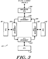
- FIG. 4 depicts a preferred structure for an exemplary processing cell 18A of the illustrated embodiment.
- the illustrated processing cell 18A includes a central processing unit 58 coupled with external device interface 60, data subcache 62 and instruction subcache 64 over processor bus 66 and instruction bus 68, respectively.
- Interface 60 provides communications with an external device, e.g., disk drive 19A, over external device bus 70, in a manner conventional to the art.
- an external device e.g., disk drive 19A
- a multiprocessing system 10 constructed in accord with a preferred embodiment of the invention permits access to individual data elements allocated to processing cells 18A, 18B, . . . 18R by reference to a unique descriptor, based on a system virtual address (SVA), associated with each datum.
- SVA system virtual address
- implementation of this capability is provided by the combined actions of the processing cell memory units in connection with their transfer of request and response packets over the network 46. In the discussion which follows, this is collectively referred to as the "memory system.”
- the illustrated system's processors e.g., processors 40A, 40B, 40C, communicate with the memory system via two primary logical interfaces.
- the first is the data access interface, which is implemented by the load and store instructions.
- the processor presents the memory system with an SVA and access mode information, and the memory system attempts to satisfy that access by finding the subpage containing the data and returning it.
- the second logical interface mode is control access, which is implemented by memory system control instructions.
- the processor instructs the memory system to perform some side effect or return some information other than the actual data from a page.
- the operating system 51 e.g., the operating system
- each processing cell contains a central processing unit (or CEU) which has a subcache that stores 0.5 MBytes of data.
- CEU central processing unit
- Those processing cells also include caches, which store 32 MBytes of data.
- a preferred level:0 having, for example, 15 processing cells stores a total of 480 MBytes.
- a preferred level:1 having, for example, 32 level:0's has a total of 15360 MBytes.
- the memory system stores data in units of pages and subpages.
- each individual cache describes 32 MBytes of SVA space, subdivided into 2048 pages. Pages contain 214 (16384) bytes, divided into 128 subpages of 27 (128) bytes.
- the memory system allocates storage in the caches on a page basis, and each page of SVA space is either entirely represented in the system or not represented at all.
- the memory system shares data between caches in units of subpages.
- the subpage states are defined in terms of three classes of subpage states: invalid, read-only, and owner. These three classes are ordered in strength according to the access that they permit. Invalid states permit no access. Read-only state permits load and instruction-fetch access. There are several owner states: all permit load access and permit the cache to respond to a data request from the network 46; some permit store access. Only one cache may hold a particular subpage in an owner state at any given time. The cache that holds a subpage in an owner state is called the owner of the subpage. Ownership of each subpage moves from cache to cache as processors request ownership via store instructions, special load instructions, and atomic state instructions (e.g., gsp or rsp) that request ownership.
- atomic state instructions e.g., gsp or rsp
- the local cache When the CEU references a subpage in invalid-descriptor state, the local cache must allocate one of the descriptors (in the correct set) to the SVA. After the descriptor allocation is complete, all subpages in the page have invalid state.
- the local cache When the local cache has a descriptor for a particular page, but a particular subpage is not present in that cache, then that subpage is in invalid state. The local cache will attempt to obtain the subpage data by communicating with other caches.
- read-only state There is only one read-only state: read-only. Any number of caches may hold a particular subpage in read-only state, provided that the owner of the subpage holds the subpage in non-exclusive state. If the owner of the subpage has any other state (i.e. an exclusive-ownership state, one of: exclusive, atomic, or transient-atomic), then no read-only copies can exist in any cell. The CEU cannot modify a subpage which is in read-only state.
- Non-exclusive and exclusive-ownership There are two basic owner state types: non-exclusive and exclusive-ownership. When a particular cache holds a particular subpage in non-exclusive state, then some other caches may be holding that subpage in read-only state. Programmatically, non-exclusive state is the same as read-only state. The CEU cannot modify a subpage which is in non-exclusive state. Non-exclusive state is basically a book-keeping state used by the memory system; it defines the ownership of the subpage.
- the exclusive-ownership states are exclusive, atomic, and transient-atomic. When a particular cache holds a particular subpage in an exclusive-ownership state, then no other cache may hold a read-only or non-exclusive copy of the subpage. If the local cache has a subpage in an exclusive-ownership state, the CEU can modify subpage data provided that the STT grants write access to the segment and the descriptor.no_write flag is clear.
- Atomic state is a stronger form of ownership than exclusive state. Subpages only enter and leave atomic state as a result of explicit requests by programs.
- atomic state can be used to single-thread access to any subpage in SVA space.
- a processor executes a gsp.nwt (get-subpage, no-wait) instruction to request that a subpage enter atomic state
- the instruction will only complete normally if the subpage is not in atomic state already.
- atomic state on a subpage can be used as a simple lock.
- the lock is locked when the gsp.nwt instruction completes normally by first obtaining the subpage in exclusive state and then changing state from exclusive to atomic.
- the lock is unlocked by executing the rsp (release-subpage) instruction.
- the rsp instruction requires that the subpage exist in some cache with atomic or transient-atomic state.
- the local cache obtains the subpage and then changes the subpage from atomic or transient-atomic state to exclusive state. (If the subpage has transient-atomic state, the operation is more complex, but the effect is programmatically the same.)
- atomic state is associated only with a subpage; there is no association with a particular operating system process (typically a user program) or to a particular cell. It is possible for a process to execute a gsp instruction to get a subpage in atomic state and subsequently be switched by operating system 51 so that it continues execution on another cell. That process continues execution on the second cell and eventually executes an rsp instruction to release the subpage. Between those two instructions, there will only be a single copy of the subpage in the entire memory system, and it will be in atomic or transient-atomic state. As various processors execute instructions which reference the subpage, that single valid copy will move from cell to cell. It is also possible for a particular process to get atomic state, and another process to release atomic state.
- Atomic state is simply an additional flag associated with a subpage; it is possible to implement protocols which use atomic state in addition to the data state of the subpage. Just as a protocol which is implemented using only data can have errors, it is possible for an atomic-state protocol to be defective. The hardware does not impose any checking on the use of atomic state beyond access control imposed by the STT and descriptor.noatomic.
- the gsp.nwt instruction always completes within its defined execution time, but it can succeed or fail (depending upon the current state of the subpage in the memory system).
- a second form of the instruction is gsp.wt (get-subpage, wait), which will not complete until the subpage is obtained in exclusive state and changed to atomic state.
- the gsp.wt instruction relieves the programmer of the burden of determining whether or not the gsp instruction was successful. If the subpage is already in atomic or transient-atomic state when a processor executes gsp.wt, the processor will stall until the subpage is released, obtained by the local cache, and changed back from exclusive state to atomic or transient-atomic state.
- Use of the gsp.wt instruction can reduce the number of messages sent between caches as a cell waits for the opportunity to "lock the lock."
- Transient-atomic state is used automatically by the memory system to allow gsp.wt to function efficiently. Its use is entirely transparent to the programmer. If a subpage is in atomic state and another cache executes gsp.wt on that subpage, that subpage enters transient-atomic state in the holding cache. When the subpage is later released with an rsp instruction, the transient-atomic state forces the subpage to be expelled onto the network 46 in a special release state. The releasing caches changes its own state for the subpage to invalid. Any cache which is executing a gsp will see the subpage and accept it. The accepting cache will then be able to complete its gsp instruction and the subpage will enter transient-atomic state in that cache.
- This operation will happen for each succeeding gsp and rsp until such time as an expelled subpage is not accepted by any other cache. At that time, the cache performing the release will change its subpage state back from invalid state (set when the subpage was released) back to exclusive state.
- Each cache directory is made up of descriptors. There is one descriptor for each page of memory in a cache. At a particular time, each descriptor is said to be valid or invalid. If a descriptor is valid, then the corresponding cache memory page is associated with a page of SVA space, and the descriptor records the associated SVA page address and state information. If a descriptor is invalid, then the corresponding cache memory page is logically not in use. There is no explicit validity flag associated with a descriptor; a descriptor may be considered invalid if the anchor and held fields are both clear, and there are no valid subpages present for the SVA page.
- Each cache directory acts as a content-addressable memory. This permits a cache to locate a descriptor for a particular page of SVA space without an iterative search through all of its descriptors.
- Each cache directory is implemented as a 16-way set-associative memory with 128 sets. All of the pages of SVA space are divided into 128 equivalence classes, each associated with a cache directory set. A descriptor for a page can only be stored in the set of a cache directory that corresponds to the page's equivalence class. The equivalence class is selected by SVA[20:14]. At any given time, a cache can describe no more than 16 pages with the same value for SVA[20:14], since there are 16 elements in each set.
- FIG. 5 A preferred organization of a cache directory is shown in Figure 5.
- the cache When a reference to an SVA is made, the cache must determine whether or not it has the required information. This is accomplished by selecting a set within the cache, and then examining all the descriptors of that set. SVA[20:14] selects a set. In the general architecture, each of the descriptors in the selected set is simultaneously compared against SVA[63:21]. In a preferred embodiment having a 240 MByte SVA space, this implies a comparison with SVA[39:21]. If one of the elements of the set is a descriptor for the desired page, the corresponding comparator will indicate a match. The index in the set of the matching descriptor, concatenated with the set number, identifies a page in the cache.
- the cache If more than one descriptor matches, the cache signals a multiple descriptor_match exception. If no descriptor matches, the cache allocates a descriptor and requests data from the network. It is possible that either the allocation or data request will fail, and the cache will indicate an error to the CEU.
- SVA[20:14] The use of SVA[20:14] to select a set is effectively a hash function over SVA addresses.
- the operating system 51 must assign SVA addresses so that this hash function gives good performance in common cases. There are two important distribution cases: referencing many pages of a single segment and referencing the first page of many segments. This set selector produces good cache behavior for contiguous groups of pages, since 128 contiguous pages will reside in 128 distinct sets. However, this selector will produce poor hashing behavior for many pages with the same value in SVA[20:14].
- the operating system 51 can avoid the latter situation by varying the logical origin of data within segments. For example, each per-process user stack can be started at a different segment offset.
- a cell When a cell responds to a request for a subpage, it supplies the subpage data and the values of certain descriptor fields in the local cache. When the response returns to the requestor it either copies those fields to descriptor fields (if it has no other valid subpages) or logically OR's those fields into descriptor fields. Some descriptor fields are never supplied by the responder nor updated by the requestor.
- the descriptor fields are defined as follows: descriptor.tag (19 bits) Bits [39:21] of an SVA. This field identifies the particular page of SVA space specified by the corresponding descriptor. For a given set in a given cell, this field must be unique among all 16 descriptors. Operating system 51 'sets' this field when it creates an SVA page. (It is also set by operating system 51 during cache initialization.) descriptor.atomic_modified (1 bit) A cache sets this bit flag to one when any subpage of this page undergoes a transition into or out of atomic state because a gsp or rsp instruction was successfully executed.
- This flag is not set if an attempt to modify data fails because descriptor.no_write is set.
- This field is propagated from cache to cache. descriptor.referenced (1 bit) The cache sets this field on references to the page and clears the field periodically. The field is used to reflect that the page was recently referenced. descriptor.anchor(1 bit) Software sets the field to indicate that data requests from other caches may not be honored nor may the descriptor be dropped. Any read or get request from another cache returns unresponded to the requestor, and is treated as if the page were missing. This field is set by operating system 51 as part of creating or destroying an SVA page, and as part of modifying the page descriptor.
- descriptor.held (1 bit) Software sets the field to indicate that the descriptor may not be dropped by the cache even if no subpages are present in the cache.
- descriptor.no_atomic (1 bit) Software sets this field to prevent any cache from changing the atomic state of any subpage of this page. An attempt to execute a gsp or rsp fails, and is signalled back to the processor. The processor signals a page_no_atomic exception. descriptor.no atomic can be altered even when some subpages have atomic state. This flag simply prevents attempt to change atomic state, in the same way that descriptor.no_write simply prevents attempts to change data state. This field is propagated from cache to cache.
- descriptor.no_write (1 bit) Software sets this field to prevent modifications to the page by the local processor. An attempt to modify the page fails, and is signalled back to the processor. The processor signals a page_no write exception. This flag does not affect the ability of any cache to acquire the subpage in exclusive or atomic/transient-atomic state. This field is propagated from cache to cache.
- descriptor.summary (3 bits) Summarizes subpage state field of a set of subpages. There is one three-bit summary field for each set of subpages. The summary sometimes overrides the contents of the individual subpage_state fields for the subpages within the summary set.
- subpage_state (4 bits) The subpage state consists of a three-bit state field and a single bit subcached status field. It is set by the cache to record the state of each subpage and to indicate whether or not any portion of the subpage is present in the CEU subcache.
- the subpage atomic instructions are the program interface to the get and release operations described above. These instructions exist in several forms to permit precise tuning of parallel programs.
- the subpage if the subpage is not in atomic state in any cache, then the local cache acquires it in atomic state.
- the @MEM condition code indicates the success or failure of the attempt; the instruction will trap instead of changing @MEM if the trap option is present in the instruction and the subpage is already atomic.
- the gsp.wt instruction form causes the cache to stall the CEU until the subpage can be obtained in atomic state. This reduces the amount of interconnect traffic if the program must obtain atomic state before it can proceed. If the subpage is already atomic in any cache (including the local cache), the instruction waits until the subpage is released. The local cache then acquires the subpage in atomic state. The @MEM condition is always changed to indicate success. release subpage [rsp] Release subpage is used to remove a subpage from atomic state. If the subpage is not present in the local cache, it is first requested in via the interconnect. Once the local cache has exclusive ownership, rsp proceeds. If the subpage is not in atomic state then release subpage does not change the subpage state.
- the CEU will trap if the trap modifier is present for the instruction. If the subpage is in atomic state, it is changed to exclusive state. If the subpage is in transient-atomic state, it is changed to exclusive state and expelled onto the interconnect so that any waiting cell may acquire atomic state.
- the system 10 handles page and descriptor in the manner described below. This discussion assumes that an anchored descriptor exists on the local cache.
- the SVA page now exists, although its data values are undefined.
- Software must initialize the page using store instructions or 1/0 before allowing the user to reference the page. For this reason, the operating system 51 will typically create a page at an SVA location inaccessible to user programs, initialize the page data, and then change the address of the SVA page as described below.
- the page is released for general use by executing an mpdw instruction which clears the anchor.
- operating system 51 After the mpsa, operating system 51 must obtain all subpages in exclusive state. This is done using mfsva instructions. The operating system 51 then executes mpdw specifying that all subpages should be changed to invalid state. This instruction causes a message to be sent on the network 46 so that any interested ring members may note the destruction of the page. The SVA page is destroyed by this operation. Software releases the descriptor for reuse by executing a second mpdw which clears the anchor.
- the mpdw instruction is used to change various fields in a local descriptor. It can set or clear the modified, atomic_modified, no_write, noatomic, and held fields and can clear the anchor field. mpdw can also change the tag, and thus the SVA space address associated with the descriptor. (Since the index of the descriptor forms part of the SVA, the new tag is in the same cache set, by definition.)
- operating system 51 must obey certain rules when altering the fields or tag of a descriptor. mpdw requires that descriptor.anchor be set (although the instruction itself may result in clearing descriptor.anchor).
- descriptor.anchor be set (although the instruction itself may result in clearing descriptor.anchor).
- Various sequences require that all subpages be present in the local cache with an exclusive-ownership state. This is accomplished by setting descriptor.anchor and executing mfsva.ex for each subpage.
- Various sequences require that all subpages be unsubcached in the local cache. This is accomplished by executing mflsp for each subpage which might be subcached in the local CEU. (Executing mfsva.ex ensures that a subpage is not subcached in by the CEU of any other cell.)
- Memory system control instructions permit the processor to directly manipulate the memory system.
- the data movement control instructions move pages and subpages of data from cache to cache in the hierarchy.
- the page state control instructions manipulate page descriptors.
- CEU instructions result in cache commands which execute synchronously or asynchronously, depending upon the command.
- a CEU cache instruction may occupy an entry in the cache PRT (a hardware table) while it is in progress.
- the PRT has four entries, so a maximum of four cache instructions may execute in parallel.
- Most of these CEU instructions result in assignment of a PRT entry which remains in use until the request is satisfied, providing synchronous behavior. For example, load/store instructions execute synchronously, so that certain software-controlled exceptions (such as missing page or unwriteable page) can be predictably resolved.
- the pcsp (prefetch-cache-subpage) and pstsp (post-store-subpage) instructions operate asynchronously, as described in following subsections.
- Synchronous errors typically result in the CEU executing the trap sequence.
- Asynchronous errors result from actual hardware errors or are provoked by a request from some other cache. Such errors are reported by memory-system interrupts.
- the mfsva instructions permits operating system 51 to fetch a subpage in read-only or exclusive-ownership state, specifying the SVA location of the subpage. This saves operating system 51 the effort of establishing a DSTT translation, as is required by pcsp.
- the mflsp instruction causes the cache to ensure that the specified subpage is not subcached in the local CEU. If the subpage is in invalid-descriptor state or invalid state, no descriptor is allocated and the subpage is not requested via the network 46.
- the mrcsp instruction allows operating system 51 to reduce the number of active descriptors for a page by causing ownership to migrate to another cache. Unlike the background recombine activity of the cache, this instruction is not controlled by cache configuration parameters.
- the page state control instructions operate on individual pages of SVA space.
- the mpsa instruction provides an anchored descriptor in the local cache for an SVA page. If the descriptor already existed prior to the mpsa, its anchor flag is set. Otherwise, the cache allocates a descriptor and then sets the anchor flag. Page state control operations require that an anchored descriptor for the SVA page be present on the local cache.
- the mpdw instruction is used to create and destroy SVA pages, and to change descriptor flags of existing SVA pages. mpdw requires that operating system 51 first obtain an anchored descriptor for the page, using the mpsa instruction.
- the operating system 51 includes a mechanism for managing data accesses and allocations. That mechanism, referred to herein as the "virtual memory” or “VM” system, performs three major functions. First, it manages the SVA space. This includes mapping of objects (files, devices, etc.) to SVA regions and the maintenance of atomic state information for those regions. Aspects of this first function are discussed in further detail in copending, commonly assigned U.S.S.N. , filed this day herewith, for DIGITAL DATA PROCESSOR WITH IMPROVED PAGING (Attorney Docket No. KSD-043).
- the VM system manages each process's context address (CA) space. This includes the mapping of CA space to a region of SVA space using the segment translation table entries (STTE's). This also includes process management and debugger support. Aspects of this second function are discussed in further detail in copending, commonly assigned U.S.S.N. , filed this day herewith, for DIGITAL DATA PROCESSOR WITH IMPROVED CHECKPOINTING & FORKING (Attorney Docket No. KSD-044).
- the VM system is responsible for resolving page faults and most of the trap conditions. Part of this task is reducing the frequency of the more severe types of faults, such as line fulls and faults that result in paging to or from devices. This is handled by attempting to make the most efficient use of the physical memory available in the system.
- At least portions of the VM system are resident on every cell, for example, for operation in conjunction with central processing units 40A, 40B, 40C.
- the caches of the illustrated system 10 are used by the operating system 51 as part of a multilevel storage system.
- physical memory is multiplexed over a large address space via demand paging.
- the caches include features that accelerate the implementation of a multilevel storage system in which software moves data between the caches and secondary storage in units of SVA pages.
- each cache can only hold a limited number of SVA pages: 2048 pages in each cache, and 16 in any particular set.
- a CEU instruction may reference an SVA page which is not present in the local cache (it is in invalid-descriptor state).
- the local cache Before issuing a request on the network 46 for the requested subpage, the local cache must allocate a descriptor by (1) finding an invalid descriptor; (2) invalidating a read-only copy; or (3) destroying a pure SVA page (i.e., a for which: all subpages are in exclusive-ownership states; no subpages are subcached; no pending instructions, e.g., GET's, are in progress as reflected in a PRT table; and descriptor.modified, descriptor.atomicmodified, descriptor.held and descriptor.anchor are all clear).
- the process of allocating descriptors will fill up the elements of a particular cache set.
- the corresponding cache control unit e.g., 52A ( Figure 2A)
- cache will not be able to allocate a descriptor in the corresponding directory, e.g., 56A, and memory element, e.g., 54A.
- the cache control unit will signal a "line-full" exception, invoking a trap handler and, thereby, the operating system 51.
- the operating system 51 can, for example, transfer a page currently in the cache line to disk, thereby opening a space in the cache (and cache line) for allocation.
- the caches can allocate needed descriptors by (1) "dropping" pages for which copies exist elsewhere in the system; (2) recombining pages for which subpages are stored in other caches; and (3) distributing pages to less active or less filled cache lines in other caches.
- descriptors in a cache set which have no valid subpages. This situation can arise as a result of requests generated by other caches, or as a result of recombining activity (described below). For example, assume that a cache descriptor has only one valid subpage, for which it has exclusive state. If some other cache requests ownership of the subpage, this cache no longer has any valid subpages of the page. If descriptor.held and descriptor.anchor are clear in this cache, then this descriptor can be reused when the CEU references some other page which has invalid-descriptor state in the same set of this cache.
- a cache will automatically drop -- i.e., invalidate the descriptor for -- a page which has all subpages in read-only or invalid state (a read-only page), provided that no subpage is subcached. This is possible because no information is lost by the memory system when it destroys read-only copies.
- the cache has configuration options to totally disable copy dropping or to restrict it to a partial range of descriptors, according to the referenced bit.
- a cache will automatically drop a page which has all subpages in some exclusive-ownership state and which has descriptor.modified and descriptor.atomic modified both clear.
- the fact that the cache has exclusive ownership of all subpages guarantees that no other cache has ownership or a copy of some portion of the data state, and allows this cache to destroy data state without communicating with any other cache.
- descriptor.modified and descriptor.atomic modified are both clear indicates that no data or atomic state change (including transition from atomic state to transient-atomic state as the result of a gsp.wt instruction) has occurred since the SVA page was created or last polled by operating system 51.
- the memory system presumes that operating system 51 has a copy of the page data and atomic state on secondary storage which can be used to recreate the SVA page, and destroys the page.
- the cache has configuration options to totally disable pure page dropping or to restrict it to a partial range of descriptors, according to the referenced bit. Note that operating system 51 must never asynchronously clear descriptor.atomicmodified if any subpage is in transient-atomic state.
- a cache issues a recombine message to recombine a subpage. If the recombine messages fail to find another cache to take over the page, the recombining cache retains the data. In effect, it has found itself as the target of the recombine. If some other cache accepts ownership (which may be non-exclusive, exclusive, atomic or transient-atomic state), the issuing cache changes its subpage state to invalid.
- the caches will automatically attempt to recombine subpages as a background activity while memory refresh is occurring.
- the cache examines a particular set, and searches for an acceptable descriptor.
- the descriptor must have no subcached subpages, must own some subpage, and must not have all subpages in exclusive-ownership state. If such a page is found, the cache issues a recombine message for some owned subpage.
- the cache has configuration options to totally disable background recombining or to restrict it to a partial range of descriptors, according to the referenced bit. Background recombining makes it more likely that the cache will be able to allocate a descriptor for a newly referenced SVA page, instead of causing a line-full error.
- operating system 51 can modify the configuration parameters which control the cache.
- the parameters for pure-dropping, copy-dropping, and background recombines can be altered to ensure that hardware actions are consistent with software working-set policy.
- Figure 6 illustrates a preferred data structure for monitoring the status of each line on each cell in the system 10 and, particularly, the number of occurrences of the line-full condition during designated time intervals referred to as "quantum" on each such cell line.
- the illustrated data structure includes a SYSTEM STATUS array having entries labelled "RING:0 #0,” “RING:0 #1,” “RING:0 #2,” and so forth, each for a respective ring:0 in the system 10.
- the entries of the SYSTEM STATUS array each hold (or point to) a RING STATUS array of the type illustrated. That array has entries labelled "CELL #0,” “CELL #1,” “CELL #2,” and so forth, each for a respective cell in the corresponding ring:0.
- the entries of the RING STATUS array each hold (or point to) a CELL STATUS array of the type illustrated. That array has entries labelled "SET #0,” “SET #1,” “SET #2,” and so forth, each for a respective one of the cache lines in the corresponding cell.
- the entries of the CELL STATUS array each hold (or point to) a LINE STATUS array having three entries, labelled "THIS QUANTUM” and “LAST QUANTUM,” reflecting the number of line-fulls in the corresponding cell line during in current and prior time intervals, respectively, as well as the number of wire pages in the line.
- the VM system initializes the LINE STATUS array to zero. Values in the entry THIS QUANTUM are incremented by the trap handler each time a line-full exception is issued. Values in the entry THIS QUANTUM are periodically transferred to the associated entry LAST QUANTUM by the procedure VM_CLEAN_LINE, discussed below; concurrently, the value in THIS QUANTUM is zeroed.
- VM_FAULT_LINE_FULL Upon signalling of a line-full exception by the cache control unit, e.g., 52A, and invoking of the trap handler, the VM system 51 executes the VM_FAULT_LINE_FULL procedure on the corresponding central processing unit.
- VM_FAULT_LINE_FULL operates synchronously to "clear" at least one page from the faulting cache line and restart the faulting process (e.g., an application program).
- the procedure VM_FAULT_LINE_FULL invokes VM_PAGE_CLEAN and VM_PAGE_TRANSFER, as described below.
- VM_FAULT_LINE_FULL accepts as input the designation of a line on a cell that caused the line-full fault.
- FIG. 7 A preferred sequence of steps for VM_FAULT_LINE_FULL is depicted in Figure 7, beginning at step 60.
- the VM system executes the VM_PAGE_CLEAN procedure on demand, e.g., when handling line-fulls VM_FAULT_LINE_FULL, and on a periodic basis, e.g., as part of background clean-up.
- the procedure can be invoked as part of a synchronous or asynchronous process.
- VM_PAGE_CLEAN When invoked, VM_PAGE_CLEAN attempts to keep at least a minimum number of pages clean on each line by dropping, recombining or transferring pages. The procedure accepts as input the address of a page to clean and produces as output a status signal.
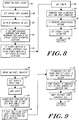
- FIG. 8 A preferred sequence of steps for VM_PAGE_CLEAN is depicted in Figure 8, beginning with step 78.
- the VM system executes the VM_PAGE_TRANSFER procedure to determine whether a first cell can take ownership of a page from a second cell. If so, it signals the first cell to take ownership.
- VM_PAGE_TRANSFER is invoked, for example, by VM_PAGE_CLEAN.
- the VM_PAGE_TRANSFER procedure accepts as input the address of a page to transfer, and produces as output a status signal.
- VM_PAGE_TRANSFER searches the data structure of Figure 6 to determine which cache has sufficient room in its corresponding cache line to accept a transferred page.
- Site-specific parameters can be utilized to determine the sequence in which candidate caches are chosen. For example, in one preferred embodiment, candidate transferee caches are chosen from among specific processing cells in the same ring:0 as the transferor cache. If the corresponding lines of all of those local caches are full, VM_PAGE_TRANSFER can choose among processing cells of other ring:0's.
- FIG. 9 A preferred sequence of steps for VM_PAGE_TRANSFER is depicted in Figure 9, beginning at step 98.
- the VM system executes the VM_PAGE_TAKE_OWNERSHIP procedure to take ownership of a page from another cell. This procedure is invoked by the intercell message handler which, in turn, carries a message signalled by another cell executing VM_PAGE_TRANSFER.
- VM_PAGE_TAKE_OWNERSHIP accepts as input the address of a page to be transferred.
- Vm_PAGE_TAKE_OWNERSHIP A preferred sequence of steps for Vm_PAGE_TAKE_OWNERSHIP is depicted in Figure 10, beginning at step 114.
- the VM system on each processing cell executes the procedure VM_CLEAN_LINE periodically to keep the number of clean pages in that cell above a threshold value, VM_LINE_FULL_TOT_HIGH.
- the procedure is preferably invoked by the software clock as part of callout queue management.
- the VM system (executing a "daemon") loops through the cell's cache trying to purify pages on lines that have had a large number of line-fulls.
- This purification is done in one of four ways: (1) by issuing a recombine of local subpages; (2) by clearing atomic-modified bits on pages that have not been modified and that contain no pages in atomic state; (3) by asking another cell to take ownership of a page; and (4) by copying a page out to disk.
- FIG. 11 A preferred sequence of steps for VM_CLEAN_LINE is depicted in Figure 11, beginning at step 122.
- the procedure VM_PAGE_SELECT determines which page in a line should be the next to be purified.
- the procedure accepts as input the line to be searched, and returns as output a candidate page.
- At least one page in each processing cell, e.g., 18A, 18B and 18C, of the system 10 is reserved by setting the "held" bit of its descriptor, i.e., descriptor.held and setting the "wired" bit in the page entry. That page is used to store those portions of the operating system 51 necessary to resolve line-full faults, as described above. This is necessary to preclude a line-full deadlock, i.e., a conflict between two (or more) cells having the same line-full condition.
- pages can also be reserved by individual cells to store, for example, portions of operating system data.
- the VM system preferably distributes those pages in the same manner that it distributes pages among multiple cells to resolve line-full faults. Therefore, any full page of kernel data may, for example, reside on a subset of cells in the system.
- the CELL STATUS array holds, within the LINE STATUS entries, the number of pages reserved in "wired" status by the corresponding cell.
- the VM system can identify cells with more then a predetermined number of wired pages. Selected held pages, for example, those holding system data (as opposed to system code or text) can be then moved to cells having fewer ones of those pages.
- FIG. 12 A preferred sequence of steps for distributing wired pages is depicted in Figure 12, beginning at step 160.
- differing data structures may be used for storing the commitment status of the cache lines. That equivalent, but varied, procedures may be used to transfer data between corresponding lines of the caches. And, by way of further example, that parameters used to determine which pages to transfer between cache lines and which caches to transfer those pages to may be varied in accord with site requirements.
Abstract
Description
- This application is related to the following co-pending and commonly assigned applications, the teachings of which are incorporated herein by reference:
- 1) United States Patent Application Serial No. 136,930, filed December 22, 1987 (Attorney Docket: KSP-001), for "MULTIPROCESSOR DIGITAL DATA PROCESSING SYSTEM;"
- 2) United States Patent Application Serial No. 696,291, filed May 20, 1991 (Attorney Docket: KSD-002C2), a continuation of United States Patent Application Serial No. 509,480, filed April 13, 1990 (Attorney Docket No. KSP-002CN), a continuation of United States patent Application Serial No. 136,701, filed December 22, 1987 (Attorney Docket No. KSP-002);
- 3) United States Patent Application No. 370,325 (Attorney Docket No. KSP-006), filed June 22, 1989, for "MULTIPROCESSOR SYSTEM WITH MULTIPLE INSTRUCTION SOURCES," a continuation-in-part of United States Patent Application Serial No. 136,930, filed December 22, 1987 (Attorney Docket No. KSP-001);
- 4) United States Patent Application No. 370,341 (Attorney Docket No. KSP-007), filed June 22, 1989, for "IMPROVED MEMORY SYSTEM FOR A MULTIPROCESSOR," a continuation of United States Patent Application Serial No. 136,930, filed December 22, 1987 (Attorney Docket No. KSP-001);
- 5) United States Patent Application No. 370,287 (Attorney Docket No. KSP-007CP), filed June 22, 1989, for "IMPROVED MULTIPROCESSOR SYSTEM," a continuation-in-part of United States Patent Application Serial No. 136,930, filed December 22, 1987 (Attorney Docket No. KSP-001);
- 6) United States Patent Application No. 499,182 (Attorney Docket No. KSP-014), filed March 26, 1990, for "HIGH-SPEED PACKET SWITCHING APPARATUS AND METHOD," a continuation-in-part of United States Patent Application Serial No. 136,930, filed December 22, 1987 (Attorney Docket No. KSP-001);
- 7) United States Patent Application No. 521,798 (Attorney Docket No. KSP-011), filed May 10, 1990, for "DYNAMIC PACKET ROUTING NETWORK," a continuation-in-part of United States Patent Application Serial No. 136,930, filed December 22, 1987 (Attorney Docket No. KSP-001), United States Patent Application Serial No. 509,480, filed April 13, 1990 (Attorney Docket No. KSP-002CN), United States Patent Application No. 370,325, filed June 22, 1989 (Attorney Docket No. KSP-006), United States Patent Application No. 370,341, filed June 22, 1989, (Attorney Docket No. KSP-007), United States Patent Application No. 370,287, filed June 22, 1989 (Attorney Docket No. KSP-007CP), United States Patent Application No. 499,182, filed March 26, 1990 (Attorney Docket No. KSP-014);
- 8) United States Patent Application No. 526,396 (Attorney Docket No. KSP-015), filed May 18, 1990, for "PACKET ROUTING SWITCH," a continuation-in-part of United States Patent Application No. 521,798, filed May 10, 1990 (Attorney Docket No. KSP-011), United States Patent Application Serial No. 136,930, filed December 22, 1987 (Attorney Docket No. KSP-001), United States Patent Application Serial No. 509,480, filed April 13, 1990 (Attorney Docket No. KSP-002CN), United States Patent Application No. 370,325, filed June 22, 1989 (Attorney Docket No. KSP-006), United States Patent Application No. 370,341, filed June 22, 1989, (Attorney Docket No. KSP-007), United States Patent Application No. 370,287, filed June 22, 1989 (Attorney Docket No. KSP-007CP), United States Patent Application No. 499,182, filed March 26, 1990 (Attorney Docket No. KSP-014);
- 9) United States Patent Application No. 531,506 (Attorney Docket No. KSP-016), filed May 31, 1990, for "DYNAMIC HIERARCHICAL ASSOCIATIVE MEMORY," a continuation-in-part of United States Patent Application Serial No. 136,930, filed December 22, 1987 (Attorney Docket No. KSP-001), United States Patent Application No. 136,701, filed December 22, 1987 (Attorney Docket No. KSP-002), United States Patent Application Serial No. 509,480, filed April 13, 1990 (Attorney Docket No. KSP-002CN), United States Patent Application No. 370,325, filed June 22, 1989 (Attorney Docket No. KSP-006), United States Patent Application No. 370,341, filed June 22, 1989, (Attorney Docket No. KSP-007), United States Patent Application No. 370,287, filed June 22, 1989 (Attorney Docket No. KSP-007CP), United States Patent Application No. 499,182, filed March 26, 1990 (Attorney Docket No. KSP-014), United States Patent Application No. 521,798, filed May 10, 1990 (Attorney Docket No. KSP-011).
- This invention relates to digital data processing and, more particularly, to moving and allocating data within a distributed memory system.
- High-speed physical storage space on computer systems is limited. Programs that run on those systems often require access to more data than that which can fit into the high-speed stores, referred to as random access memory, or RAM. Sometimes the programs themselves -- not just the data they process -- consume more memory than is available on the system.
- Early programs managed excess data by moving it directly between memory and disk as needed. This required little memory -- just the space needed to store the data currently being processed -- but slowed processing by requiring frequent disk accesses. Some gains were obtained by accessing data in blocks, reading large amounts of data from disk into arrays, processing those arrays, then writing them back out to disk.
- With the advent of virtual memory management systems, data management functions have been taken over by the computer operating system software. Programs written for use with these systems reference large amounts of data as if stored entirely in memory. Often it is not: the virtual memory system itself moves data back and forth between physical memory and disk.
- Data management and allocation becomes more complicated in computer systems which employ distributed memory, i.e., a plurality of distinct memory elements storing data from one or more processors. An example of such a system is disclosed by Frank at al, United States Patent Application Serial No. 136,930, filed December 22, 1987 (Attorney Docket KSP-001). There a digital data processing system is said to comprise a plurality of processing cells arranged in a hierarchy of rings. The processing cells include central processing units coupled with memory elements. Groups of cells are interconnected along unidirectional bus rings to form units referred to as segments. Communications between cells of different domain(0) segments are carried out on higher level information transfer domains. These higher level domains are themselves made up of one or more segments, each comprising a plurality of routing elements coupled via a unidirectional bus ring.
- A system of the type described by Frank et al does not require a main memory element, i.e., a memory element coupled to and shared by the systems many processors. Rather, data maintained by the system is distributed, both on exclusive and shared bases, among the memory elements associated with those processors. Modifications to datum stored exclusively in any one processing cell do not have to be communicated along the bus structure to other storage areas. Accordingly, only that data which the processors dynamically share, e.g., sharing required by the executing program themselves, must be transmitted along the bus structure.
- Although the Frank et al system provides mechanisms, such as the "recombine" operation for allocating data in the system, still further advances in this area are desirable.
- Accordingly, an object of this invention is to provide an improved digital data processing system.
- More particularly, an object is to provide a distributed memory digital data processing system with improved memory management.
- Still another object of the invention is to provide a mechanism for managing data effectively and reducing paging in a distributed memory system.
- These objects are attained by the invention which provides, in one aspect, a digital data processing system with shared, distributed memory which transfers data between corresponding data sets within memory.
- More particularly, the invention provides in one aspect, a digital data processor having a plurality of processing cells interconnected, for example, by a hierarchical network. Each of the processing cells includes a central processing unit and a memory element. The storage space within each memory is arranged in sets, each capable of holding a plurality of data pages. For example, each set can hold pages having common high-order address bits.
- At least a first processing cell includes page distribution means for determining when at least a first set in the associated memory has reached a predetermined storage commitment condition -- e.g., that the set is filled. Under such a condition, the page distribution means invokes a page-transfer element that selects a candidate processing cell from among the other cells and transfers one or more pages from the first set to a corresponding set in the candidate cell.
- In a related aspect of the invention, the page-transfer element generates and transmits on the network a signal representing a request for transfer of pages from the first set. Correspondingly, the candidate processing cell includes a take-ownership element for responding to the transfer request for generating a request for ownership access to the page.
- Control units coupled to the first and second processing cells respond to that ownership request for allocating, exclusively, within the corresponding set of the candidate cell memory physical storage space for the pages to be transferred; transferring those pages to that allocated space; and deallocating the physical storage space that previously stored the transferred pages in the first set (or making that space available for reallocation).
- According to another aspect of the invention, the central processing unit of the first processing cell generates a local request for access to a page. The control unit responds to at least selected ones of those requests -- e.g., requests which require allocation of a page in a set that is already full -- for generating a line-full signal. A line-full element in the page distribution element responds to the line-full condition by invoking the page-transfer means.
- In another aspect, a digital data processor of the type described above includes a table for storing a commitment status of the sets in the processing cell memories. Higher-level entries within the table corresponds to sets, while lower-level ones reflect the status of that set in a specific memory element.
- The page distribution element can respond to predetermined parameters for determining which pages in the first set to transfer. Those parameters can call, for example, for choosing for transfer certain modified pages for which no subpages are subcached.
- Further, a wired page mechanism can be utilized to prevent selected pages within a set from being selected for transfer. This feature can be used, for example, to insure that storage space is reserved for critical operating system functions and data.
- Moreover, the page distribution element can determine the cell to which to send the transfer request, as well as the pages to transfer, based on predetermined parameters. Candidate cells, for example, can be chosen based on locality to the cell that is attempting to transfer pages.
- According to still another aspect of the invention, in the event the first processing cell is unable to transfer pages from an overly committed set within a selected period, it can transfer those pages directly to disk or other secondary storage device.
- These and other objects are evident in the drawings and in the description below.
- A fuller understanding of the invention may be attained by reference to the drawings, in which:
- Figure 1 depicts the structure of a multiprocessing system for use in a preferred practice of the invention;
- Figures 2A - 2B depict a preferred memory configuration and data management operation for the multiprocessor of Figure 1;
- Figure 3 depicts a preferred configuration for an exemplary level:0 segment of the multiprocessing system of Figure 1;
- Figure 4 depicts a preferred structure for processing cells of the multiprocessing system of Figure 1;
- Figure 5 depicts a preferred structure of a cache directory of the multiprocessing system of Figure 1;
- Figure 6 depicts a preferred data structure for monitoring the status of each cache line (or memory set) on each cell in the multiprocessing system of Figure 1;
- Figure 7 depicts a preferred sequence of steps taken by a processing cell to handle a cache line-full exception within the multiprocessing system of Figure 1; and
- Figures 8 - 11 depict a preferred sequence of steps taken by a processing cell to transfer pages from a cache line in one cell to another cell within the multiprocessing system of Figure 1.
- Figure 12 depicts a preferred sequence of steps taken by a processing cell to transfer "wired" pages between cells within the multiprocessing system of Figure 1.
- Figure 1 depicts a preferred multiprocessing system used to practice the invention. The illustrated
system 10 includes three information transfer levels: level:0, level:1, and level:2. Each information transfer level includes one or more level segments, characterized by a bus element and a plurality of interface elements. Particularly, level:0 of the illustratedsystem 10 includes six segments, designated 12A, 12B, 12C, 12D, 12E and 12F, respectively. Similarly, level:1 includessegments 14A and 14B, while level:2 includessegment 16. - Each segment of level:0, i.e.,
segments 12A, 12B, ... 12F, comprise a plurality of processing cells. For example,segment 12A includescells cells - Certain cells of the
processing system 10 are connected to secondary storage devices. In the illustrated system, for example,cell 18C is coupled with disk drive 19A,cell 18D is coupled with disk drive 19B, and cell 18O is coupled with disk drive 19C. The disk drives 19A - 19C are of conventional design and can be selected from any of several commercially available devices. It will be appreciated that secondary storage devices other than disk drives, e.g., tape drives, can also be used to store information. - As further illustrated, each level:0 segment may be characterized as having a bus element providing a communication pathway for transferring information packets between the cells of the segment. Thus, illustrated
segment 12A is characterized bybus 20A, segment 12B by 20B,segment 12C by 20C, et cetera. As described in greater detail below, digital information packets are passed between thecells exemplary segment 12A by way of the memory elements associated with each of those cells. Specific interfaces between those memory elements and thebus 20A are provided bycell interface units segments 12B, 12C and 12D between theirrespective cells cell interface units 22D, 22E, ... 22R, as illustrated. - As shown in the illustration and noted above, the remaining information transfer levels, i.e., level:1 and level:2, each include one or more corresponding level segments. The number of segments in each successive segment being less than the number of segments in the prior one. Thus, level:1's two
segments 14A and 14B number fewer than level:0's six 12A, 12B ... 12F, while level:2, having onlysegment 16, includes the fewest of all. Each of the segments in level:1 and level:2, the "higher" levels, include a bus element for transferring packets within the respective segments. In the illustration, level:1segments 14A and 14B includebus elements 24A and 24B, respectively, while level:2segment 16 includesbus element 26. - The routing cells themselves provide a mechanism for transferring information between associated segments of successive levels.
Routing cells segment 14A and each of level:0segments routing cells 28D, 28b and 28F provide a means for transferring information to and from level:1 segment 14B and each of level:0segments routing cells segment 16 and level:1segments 14A and 14B, as shown. - The routing cells interface their respective segments via interconnections at the bus elements. Thus, routing
cell 28A interfacesbus elements ring interconnects bus elements 20B and 24B at ring interconnects 32B and 34B, respectively, and so forth. Similarly,routing cells ring interconnects - Figure 2A illustrates a mechanism for data movement within the processing system of Figure 1 for insuring data coherence. In the drawing, plural central processing units 40(A), 40(B) and 40(C) are coupled, respectively, to associated memory elements 42(A), 42(B) and 42(C). Communications between the processing and memory units of each pair are carried along
buses Network 46, representing the aforementioned level segments and routing cells, transfers information packets (passed to thenetwork 46 over buses 48(A), 48(B) and 48(C) between the illustratedprocessing cells 42A - 42C. - In the illustrated embodiment, the
central processing units memory elements elements access request elements - The
central processing units portions system 10 facilities, and includes a virtual memory management system for managing data accesses and allocations. - A preferred operating system for controlling
central processing units - The
memory elements cache control units data storage area corresponding directory element Stores store 54A maintains data and control information used byCPU 40A, whilestores central processing units memory elements - Access requests generated by the
central Processing units cache control units central processing units storage element cache control unit network 46 alonglines - As that packet travels within the networks and, particulary, along the ring:0 segments, cache control units within the processing cells check their own directories, passing the requested data, if found, in a response packet. Likewise the local routing element checks its directory. If that directory shows that the requested data is present in local ring in the proper access state, the routing cell permits the request packet to continue along the local ring bus. If not, the routing cell extracts the packet and passes to the associated level:1 segment.
- The unresolved request packet travels along the level:1 segment in a similar fashion, i.e., it is compared with the directories of the associated level:1 routing cells. If one of those directories lists the requested data in the proper access state in a descendant level:0 segment, the request is passed to that segment. Otherwise, the request packet may pass to a higher level, if any, in the hierarchy or be returned to the requester unresolved.
- Packets containing requested data are routed back to requesting cells by differing mechanisms. A first mechanism relies on the address, or ID, of the requesting cell. Here, each requesting cell includes within its request packet an ID uniquely identifying that cell. Once that packet reaches the responding cell, that cell copies the requestor-ID, along with the datum and corresponding descriptor, into the response packet. As the response packet travels along the segments rings, the routing cells examine the requestor-ID to determine whether the requesting cell is in a descendant or parent segment and route the packet accordingly.
- A second mechanism is used in conjunction with response packets that include data requested by processing cells but not specifically generated in response to those requests. By way of example, the mechanism applies in instances where two or more requesting cells generate requests for read-only copies to a specific datum held in a remote cell.
- Presuming, in accord with one preferred practice of the invention, that the network prevents at least some, but not all, of those requests from reaching a processing cell having a copy of that datum, the responding cell generates response packets bearing only the requestor-ID of a request packet that reached it.
- Data coherency is maintained by cooperative action of the processing cells in response to data requests and transfers. More particularly, concurrent with generation of an ownership-access request packet by a first processing cell, the associated memory allocates in its store physical space to hold the requested data. Likewise, concurrent with the transfer of a requested datum from the processing cell in which it was previously stored, the associated memory deallocates physical storage space which had been previously allocated for storage of the requested datum.
- These cooperative actions are illustrated in Figures 2A and 2B. In the first of those drawings, DATUM(0), DATUM(1) and DATUM(2), representing data subpages, are retained in the store of the
memory element 42A partnered withCPU 40A. Descriptors "foo," "bar" and "bas" which correspond, respectively, to those data stored indirectory 56A. Each such descriptor includes a pointer indicating the location of its associated information signal in thestore 42A. - The
memory element 42B partnered toCPU 40B stores DATUM(2) and DATUM(3), which also represents a data subpage. Corresponding to each of those data elements are descriptors "car" and "bas," retained in directory 56B. DATUM(2), and its descriptor "bas," are copied fromstore 42A and, therefore, retain the same labels. - The system illustrated in Figure 2A does not store any data in the
memory element 54C partnered toCPU 40C. - Figure 2B illustrates how a datum moves in conjunction with an ownership for it by processing cell which does not already have access to that datum. In particular, the illustration depicts the movement of DATUM(0) following issuance of an unresolved request for ownership for it by the processing cell made up of
CPU 40C andmemory 42C. At the outset, concurrent with the request, thecache control unit 52C allocates physical storage space in thestore 54C ofmemory element 42C. - A response packet generated by
memory 42A transfers the requested data, DATUM(0), fromstore 54A, where it had previously been stored, to the requestor'sstore 54C. Concurrently thecache control unit 52A deallocates that space instore 54A which had previously held the requested datum. At the same time, thecache control unit 52A effects invalidation of the descriptor "foo" indirectory 56A (where it had previously been used to identify DATUM(0) instore 54A), whilecache control unit 52C reallocates that same descriptor indirectory 56C, where it will subsequently be used to identify the signal instore 54C. - In addition to descriptors, the
memory elements 42A - 42C assign access state information to the data and control signals in their respective stores. These access states, which include the invalid, read-only, ownership and atomic states, govern the manner in which data may be accessed by specific processors. A datum which is stored in a memory element whose associated CPU maintains modification access over that datum is assigned an ownership state. While, a datum which is stored in a memory element whose associated CPU does not maintain priority access over that datum is assigned a read-only state. Further, a purported datum which associated with "bad" data is assigned the invalid state. - A further appreciation of preferred structures (e.g., cache control units) for data movement and memory coherence in a digital data processing system constructed in accord with the invention may be had by reference to the above-cited related applications, e.g., U.S.S.N. 136,930, filed December 22, 1987, (Attorney Docket No. KSP-001) and U.S.S.N. 370,287, filed June 22, 1989, (Attorney Docket No. KSP-007CP), U.S.S.N. 521,798, filed May 10, 1990, (Attorney Docket No. KSP-011), U.S.S.N. 531,506, filed May 31, 1990, (Attorney Docket No. KSP-016).
- Figure 3 depicts a preferred configuration for exemplary level:0
segment 12A of Figure 1. Thesegment 12A includesprocessing cells cell interconnects 22A, 22B and 22c alongbus segment 20A.Routing unit 28A provides an interconnection between the level:0segment 12A and if parent, level:1 segment 14a of Figure 1. Thisrouting unit 28A is coupled alongbus 20A by way ofcell interconnect 32A, as shown. The structure of illustratedbus segment 20A, as well as its interrelationship withcell interconnects - Figure 4 depicts a preferred structure for an
exemplary processing cell 18A of the illustrated embodiment. The illustratedprocessing cell 18A includes acentral processing unit 58 coupled withexternal device interface 60, data subcache 62 andinstruction subcache 64 overprocessor bus 66 andinstruction bus 68, respectively. -
Interface 60 provides communications with an external device, e.g., disk drive 19A, overexternal device bus 70, in a manner conventional to the art. - A more complete understanding of the circuitry illustrated in this drawing may be attained by reference to the above-cited related patent applications, e.g., Serial Nos. 136,930, filed December 22, 1987 (Attorney Docket No. KSP-001), 370,325, filed June 22, 1989 (Attorney Docket No. KSP-006), and 499,182, filed March 26, 1990 (Attorney Docket No. KSP-014).
- As discussed above, a
multiprocessing system 10 constructed in accord with a preferred embodiment of the invention permits access to individual data elements allocated to processingcells system 10, implementation of this capability is provided by the combined actions of the processing cell memory units in connection with their transfer of request and response packets over thenetwork 46. In the discussion which follows, this is collectively referred to as the "memory system." - The illustrated system's processors, e.g.,
processors - The second logical interface mode is control access, which is implemented by memory system control instructions. In control access, the processor instructs the memory system to perform some side effect or return some information other than the actual data from a page. In addition to the primary interfaces, the operating system 51 (e.g., the operating system) uses control locations in SPA space for configuration, maintenance, fault recovery, and diagnosis.
- The memory system implements a hierarchy of storage. In the illustrated, preferred embodiment, each processing cell contains a central processing unit (or CEU) which has a subcache that stores 0.5 MBytes of data. Those processing cells also include caches, which store 32 MBytes of data. Moreover, a preferred level:0 having, for example, 15 processing cells stores a total of 480 MBytes. While, a preferred level:1 having, for example, 32 level:0's has a total of 15360 MBytes.
- The memory system stores data in units of pages and subpages. For example, in the illustrated embodiment, each individual cache describes 32 MBytes of SVA space, subdivided into 2048 pages. Pages contain 2¹⁴ (16384) bytes, divided into 128 subpages of 2⁷ (128) bytes. The memory system allocates storage in the caches on a page basis, and each page of SVA space is either entirely represented in the system or not represented at all. The memory system shares data between caches in units of subpages.
- When a page of SVA space is resident in the system, the following are true:
- (1) One or more caches allocates a page of storage to the page, each subpage of the page is stored on one or more of the caches with space allocated, but
- (2) Each cache with space allocated for a page may or may not contain a copy of all (or any) of the page's subpages.
- A further appreciation of a preferred memory system for use in a digital data processing system constructed in accord with the invention may be had by reference to the above-cited related applications, e.g., U.S.S.N. 136,930, filed December 22, 1987, (Attorney Docket No. KSP-001) and U.S.S.N. 370,287, filed June 22, 1989, (Attorney Docket No. KSP-007CP), U.S.S.N. 521,798, filed May 10, 1990, (Attorney Docket No. KSP-011), U.S.S.N. 531,506, filed May 31, 1990, (Attorney Docket No. KSP-016).
- The subpage states are defined in terms of three classes of subpage states: invalid, read-only, and owner. These three classes are ordered in strength according to the access that they permit. Invalid states permit no access. Read-only state permits load and instruction-fetch access. There are several owner states: all permit load access and permit the cache to respond to a data request from the
network 46; some permit store access. Only one cache may hold a particular subpage in an owner state at any given time. The cache that holds a subpage in an owner state is called the owner of the subpage. Ownership of each subpage moves from cache to cache as processors request ownership via store instructions, special load instructions, and atomic state instructions (e.g., gsp or rsp) that request ownership. - When a subpage is not present in a cache, it is said to be in an invalid state with respect to that cache. If a processor requests a load or store to a subpage which is in an invalid state in its local cache, then that cache must request a copy of the subpage in some other state in order to satisfy the data access. There are two invalid states: invalid-descriptor and invalid.
- When a particular cache has no descriptor for a particular page, then all of the subpages of that page are said to be in invalid-descriptor state in that cache. Thus, subpages in invalid-descriptor state are not explicitly represented in the cache.
- When the CEU references a subpage in invalid-descriptor state, the local cache must allocate one of the descriptors (in the correct set) to the SVA. After the descriptor allocation is complete, all subpages in the page have invalid state.
- When the local cache has a descriptor for a particular page, but a particular subpage is not present in that cache, then that subpage is in invalid state. The local cache will attempt to obtain the subpage data by communicating with other caches.
- There is only one read-only state:
read-only. Any number of caches may hold a particular subpage in read-only state, provided that the owner of the subpage holds the subpage in non-exclusive state. If the owner of the subpage has any other state (i.e. an exclusive-ownership state, one of: exclusive, atomic, or transient-atomic), then no read-only copies can exist in any cell. The CEU cannot modify a subpage which is in read-only state. - There are two basic owner state types:
non-exclusive and exclusive-ownership. When a particular cache holds a particular subpage in non-exclusive state, then some other caches may be holding that subpage in read-only state. Programmatically, non-exclusive state is the same as read-only state. The CEU cannot modify a subpage which is in non-exclusive state. Non-exclusive state is basically a book-keeping state used by the memory system; it defines the ownership of the subpage. - The exclusive-ownership states are exclusive, atomic, and transient-atomic. When a particular cache holds a particular subpage in an exclusive-ownership state, then no other cache may hold a read-only or non-exclusive copy of the subpage. If the local cache has a subpage in an exclusive-ownership state, the CEU can modify subpage data provided that the STT grants write access to the segment and the descriptor.no_write flag is clear.
- Atomic state is a stronger form of ownership than exclusive state. Subpages only enter and leave atomic state as a result of explicit requests by programs.
- Fundamentally, atomic state can be used to single-thread access to any subpage in SVA space. When a processor executes a gsp.nwt (get-subpage, no-wait) instruction to request that a subpage enter atomic state, the instruction will only complete normally if the subpage is not in atomic state already. Thus, atomic state on a subpage can be used as a simple lock. The lock is locked when the gsp.nwt instruction completes normally by first obtaining the subpage in exclusive state and then changing state from exclusive to atomic. The lock is unlocked by executing the rsp (release-subpage) instruction. The rsp instruction requires that the subpage exist in some cache with atomic or transient-atomic state. The local cache obtains the subpage and then changes the subpage from atomic or transient-atomic state to exclusive state. (If the subpage has transient-atomic state, the operation is more complex, but the effect is programmatically the same.)
- It is important to note that atomic state is associated only with a subpage; there is no association with a particular operating system process (typically a user program) or to a particular cell. It is possible for a process to execute a gsp instruction to get a subpage in atomic state and subsequently be switched by operating system 51 so that it continues execution on another cell. That process continues execution on the second cell and eventually executes an rsp instruction to release the subpage. Between those two instructions, there will only be a single copy of the subpage in the entire memory system, and it will be in atomic or transient-atomic state. As various processors execute instructions which reference the subpage, that single valid copy will move from cell to cell. It is also possible for a particular process to get atomic state, and another process to release atomic state.
- Atomic state is simply an additional flag associated with a subpage; it is possible to implement protocols which use atomic state in addition to the data state of the subpage. Just as a protocol which is implemented using only data can have errors, it is possible for an atomic-state protocol to be defective. The hardware does not impose any checking on the use of atomic state beyond access control imposed by the STT and descriptor.noatomic.
- The gsp.nwt instruction always completes within its defined execution time, but it can succeed or fail (depending upon the current state of the subpage in the memory system). A second form of the instruction is gsp.wt (get-subpage, wait), which will not complete until the subpage is obtained in exclusive state and changed to atomic state. The gsp.wt instruction relieves the programmer of the burden of determining whether or not the gsp instruction was successful. If the subpage is already in atomic or transient-atomic state when a processor executes gsp.wt, the processor will stall until the subpage is released, obtained by the local cache, and changed back from exclusive state to atomic or transient-atomic state. Use of the gsp.wt instruction can reduce the number of messages sent between caches as a cell waits for the opportunity to "lock the lock."
- Transient-atomic state is used automatically by the memory system to allow gsp.wt to function efficiently. Its use is entirely transparent to the programmer. If a subpage is in atomic state and another cache executes gsp.wt on that subpage, that subpage enters transient-atomic state in the holding cache. When the subpage is later released with an rsp instruction, the transient-atomic state forces the subpage to be expelled onto the
network 46 in a special release state. The releasing caches changes its own state for the subpage to invalid. Any cache which is executing a gsp will see the subpage and accept it. The accepting cache will then be able to complete its gsp instruction and the subpage will enter transient-atomic state in that cache. This operation will happen for each succeeding gsp and rsp until such time as an expelled subpage is not accepted by any other cache. At that time, the cache performing the release will change its subpage state back from invalid state (set when the subpage was released) back to exclusive state. - A further appreciation of preferred subpage states used in a digital data processing system constructed in accord with the invention may be had by reference to the above-cited related applications, e.g., U.S.S.N. 136,930, filed December 22, 1987, (Attorney Docket No. KSP-001), U.S.S.N. 370,287, filed June 22, 1989, (Attorney Docket No. KSP-007CP), U.S.S.N. 521,798, filed May 10, 1990, (Attorney Docket No. KSP-011), and U.S.S.N. 531,506, filed May 31, 1990, (Attorney Docket No. KSP-016).
- The associations between cache pages and SVA pages are recorded by each cache in its cache directory. Each cache directory is made up of descriptors. There is one descriptor for each page of memory in a cache. At a particular time, each descriptor is said to be valid or invalid. If a descriptor is valid, then the corresponding cache memory page is associated with a page of SVA space, and the descriptor records the associated SVA page address and state information. If a descriptor is invalid, then the corresponding cache memory page is logically not in use. There is no explicit validity flag associated with a descriptor; a descriptor may be considered invalid if the anchor and held fields are both clear, and there are no valid subpages present for the SVA page.
- Each cache directory acts as a content-addressable memory. This permits a cache to locate a descriptor for a particular page of SVA space without an iterative search through all of its descriptors. Each cache directory is implemented as a 16-way set-associative memory with 128 sets. All of the pages of SVA space are divided into 128 equivalence classes, each associated with a cache directory set. A descriptor for a page can only be stored in the set of a cache directory that corresponds to the page's equivalence class. The equivalence class is selected by SVA[20:14]. At any given time, a cache can describe no more than 16 pages with the same value for SVA[20:14], since there are 16 elements in each set.
- A preferred organization of a cache directory is shown in Figure 5. When a reference to an SVA is made, the cache must determine whether or not it has the required information. This is accomplished by selecting a set within the cache, and then examining all the descriptors of that set. SVA[20:14] selects a set. In the general architecture, each of the descriptors in the selected set is simultaneously compared against SVA[63:21]. In a preferred embodiment having a 240 MByte SVA space, this implies a comparison with SVA[39:21]. If one of the elements of the set is a descriptor for the desired page, the corresponding comparator will indicate a match. The index in the set of the matching descriptor, concatenated with the set number, identifies a page in the cache.
- If more than one descriptor matches, the cache signals a multiple descriptor_match exception. If no descriptor matches, the cache allocates a descriptor and requests data from the network. It is possible that either the allocation or data request will fail, and the cache will indicate an error to the CEU.
- The use of SVA[20:14] to select a set is effectively a hash function over SVA addresses. The operating system 51 must assign SVA addresses so that this hash function gives good performance in common cases. There are two important distribution cases: referencing many pages of a single segment and referencing the first page of many segments. This set selector produces good cache behavior for contiguous groups of pages, since 128 contiguous pages will reside in 128 distinct sets. However, this selector will produce poor hashing behavior for many pages with the same value in SVA[20:14]. The operating system 51 can avoid the latter situation by varying the logical origin of data within segments. For example, each per-process user stack can be started at a different segment offset.
- When a cell responds to a request for a subpage, it supplies the subpage data and the values of certain descriptor fields in the local cache. When the response returns to the requestor it either copies those fields to descriptor fields (if it has no other valid subpages) or logically OR's those fields into descriptor fields. Some descriptor fields are never supplied by the responder nor updated by the requestor.
- In a preferred embodiment, the descriptor fields are defined as follows:
descriptor.tag (19 bits)
Bits [39:21] of an SVA. This field identifies the particular page of SVA space specified by the corresponding descriptor. For a given set in a given cell, this field must be unique among all 16 descriptors. Operating system 51 'sets' this field when it creates an SVA page. (It is also set by operating system 51 during cache initialization.)
descriptor.atomic_modified (1 bit)
A cache sets this bit flag to one when any subpage of this page undergoes a transition into or out of atomic state because a gsp or rsp instruction was successfully executed. It is also set when a subpage changes from atomic state to transient-atomic state. This flag is not set if a gsp fails because the subpage is already in atomic state or if a rsp fails because the subpage was not in atomic state. This flag is not set if the gsp or rsp fails because descriptor.noatomic is set. Operating system 51 sets this flag to zero to indicate that it has noted the atomic state changes. This field is propagated from cache to cache.
descriptor.modified (1 bit)
A cache sets this bit flag to one when any data is modified in the page. Operating system 51 sets descriptor.modified to zero to indicate that it has noted the modification of the page. This flag is not set if an attempt to modify data fails because descriptor.no_write is set. This field is propagated from cache to cache.
descriptor.referenced (1 bit)
The cache sets this field on references to the page and clears the field periodically. The field is used to reflect that the page was recently referenced.
descriptor.anchor(1 bit)
Software sets the field to indicate that data requests from other caches may not be honored nor may the descriptor be dropped. Any read or get request from another cache returns unresponded to the requestor, and is treated as if the page were missing. This field is set by operating system 51 as part of creating or destroying an SVA page, and as part of modifying the page descriptor.
descriptor.held (1 bit)
Software sets the field to indicate that the descriptor may not be dropped by the cache even if no subpages are present in the cache.
descriptor.no_atomic (1 bit)
Software sets this field to prevent any cache from changing the atomic state of any subpage of this page. An attempt to execute a gsp or rsp fails, and is signalled back to the processor. The processor signals a page_no_atomic exception. descriptor.no atomic can be altered even when some subpages have atomic state. This flag simply prevents attempt to change atomic state, in the same way that descriptor.no_write simply prevents attempts to change data state. This field is propagated from cache to cache.
descriptor.no_write (1 bit)
Software sets this field to prevent modifications to the page by the local processor. An attempt to modify the page fails, and is signalled back to the processor. The processor signals a page_no write exception. This flag does not affect the ability of any cache to acquire the subpage in exclusive or atomic/transient-atomic state. This field is propagated from cache to cache.
descriptor.summary (3 bits)
Summarizes subpage state field of a set of subpages. There is one three-bit summary field for each set of subpages. The summary sometimes overrides the contents of the individual subpage_state fields for the subpages within the summary set.
descriptor.subpage_state (4 bits)
The subpage state consists of a three-bit state field and a single bit subcached status field. It is set by the cache to record the state of each subpage and to indicate whether or not any portion of the subpage is present in the CEU subcache. - A further appreciation of preferred structures for the cache directory and descriptors in a digital data processing system constructed in accord with the invention may be had by reference to the above-cited related applications, e.g., U.S.S.N. 136,930, filed December 22, 1987, (Attorney Docket No. KSP-001), U.S.S.N. 370,287, filed June 22, 1989, (Attorney Docket no. KSP-007CP), U.S.S.N. 521,798, filed May 10, 1990, (Attorney Docket No. KSP-011), and U.S.S.N. 531,506, filed May 31, 1990, (Attorney Docket No. KSP-016).
- The subpage atomic instructions are the program interface to the get and release operations described above. These instructions exist in several forms to permit precise tuning of parallel programs.
get subpage [gsp.nwt]
get subpage & wait [gsp.wt]
Get subpage requests that a subpage be set into atomic state. For both forms of the get subpage instruction, if the subpage is not in atomic state in any cache, then the local cache acquires it in atomic state.
For gsp.nwt, the @MEM condition code indicates the success or failure of the attempt; the instruction will trap instead of changing @MEM if the trap option is present in the instruction and the subpage is already atomic.
The gsp.wt instruction form causes the cache to stall the CEU until the subpage can be obtained in atomic state. This reduces the amount of interconnect traffic if the program must obtain atomic state before it can proceed. If the subpage is already atomic in any cache (including the local cache), the instruction waits until the subpage is released. The local cache then acquires the subpage in atomic state. The @MEM condition is always changed to indicate success.
release subpage [rsp]
Release subpage is used to remove a subpage from atomic state. If the subpage is not present in the local cache, it is first requested in via the interconnect. Once the local cache has exclusive ownership, rsp proceeds. If the subpage is not in atomic state then release subpage does not change the subpage state. In this situation, the CEU will trap if the trap modifier is present for the instruction. If the subpage is in atomic state, it is changed to exclusive state. If the subpage is in transient-atomic state, it is changed to exclusive state and expelled onto the interconnect so that any waiting cell may acquire atomic state. - The
system 10 handles page and descriptor in the manner described below. This discussion assumes that an anchored descriptor exists on the local cache. - Following the mpsa, the descriptor exists, but all subpages are in invalid state. Operating system 51 executes mpdw specifying that all subpage states should be set to exclusive. This causes a message to be sent on the
network 46 so that any interested ring members may note the creation of the page. - The SVA page now exists, although its data values are undefined. Software must initialize the page using store instructions or 1/0 before allowing the user to reference the page. For this reason, the operating system 51 will typically create a page at an SVA location inaccessible to user programs, initialize the page data, and then change the address of the SVA page as described below. The page is released for general use by executing an mpdw instruction which clears the anchor.
- After the mpsa, operating system 51 must obtain all subpages in exclusive state. This is done using mfsva instructions. The operating system 51 then executes mpdw specifying that all subpages should be changed to invalid state. This instruction causes a message to be sent on the
network 46 so that any interested ring members may note the destruction of the page. The SVA page is destroyed by this operation. Software releases the descriptor for reuse by executing a second mpdw which clears the anchor. - The mpdw instruction is used to change various fields in a local descriptor. It can set or clear the modified, atomic_modified, no_write, noatomic, and held fields and can clear the anchor field. mpdw can also change the tag, and thus the SVA space address associated with the descriptor. (Since the index of the descriptor forms part of the SVA, the new tag is in the same cache set, by definition.)
- To ensure memory system consistency, operating system 51 must obey certain rules when altering the fields or tag of a descriptor. mpdw requires that descriptor.anchor be set (although the instruction itself may result in clearing descriptor.anchor). Various sequences require that all subpages be present in the local cache with an exclusive-ownership state. This is accomplished by setting descriptor.anchor and executing mfsva.ex for each subpage. Various sequences require that all subpages be unsubcached in the local cache. This is accomplished by executing mflsp for each subpage which might be subcached in the local CEU. (Executing mfsva.ex ensures that a subpage is not subcached in by the CEU of any other cell.)
- Memory system control instructions permit the processor to directly manipulate the memory system. There are two classes of control instructions: data movement and page state control. The data movement control instructions move pages and subpages of data from cache to cache in the hierarchy. The page state control instructions manipulate page descriptors.
- These CEU instructions result in cache commands which execute synchronously or asynchronously, depending upon the command. A CEU cache instruction may occupy an entry in the cache PRT (a hardware table) while it is in progress. The PRT has four entries, so a maximum of four cache instructions may execute in parallel. Most of these CEU instructions result in assignment of a PRT entry which remains in use until the request is satisfied, providing synchronous behavior. For example, load/store instructions execute synchronously, so that certain software-controlled exceptions (such as missing page or unwriteable page) can be predictably resolved. The pcsp (prefetch-cache-subpage) and pstsp (post-store-subpage) instructions operate asynchronously, as described in following subsections.
- Synchronous errors typically result in the CEU executing the trap sequence.
- Asynchronous errors result from actual hardware errors or are provoked by a request from some other cache. Such errors are reported by memory-system interrupts.
- The mfsva instructions permits operating system 51 to fetch a subpage in read-only or exclusive-ownership state, specifying the SVA location of the subpage. This saves operating system 51 the effort of establishing a DSTT translation, as is required by pcsp.
- The mflsp instruction causes the cache to ensure that the specified subpage is not subcached in the local CEU. If the subpage is in invalid-descriptor state or invalid state, no descriptor is allocated and the subpage is not requested via the
network 46. - The mrcsp instruction allows operating system 51 to reduce the number of active descriptors for a page by causing ownership to migrate to another cache. Unlike the background recombine activity of the cache, this instruction is not controlled by cache configuration parameters.
- The page state control instructions operate on individual pages of SVA space.
- The mpsa instruction provides an anchored descriptor in the local cache for an SVA page. If the descriptor already existed prior to the mpsa, its anchor flag is set. Otherwise, the cache allocates a descriptor and then sets the anchor flag. Page state control operations require that an anchored descriptor for the SVA page be present on the local cache.
- The mpdw instruction is used to create and destroy SVA pages, and to change descriptor flags of existing SVA pages. mpdw requires that operating system 51 first obtain an anchored descriptor for the page, using the mpsa instruction.
- A further appreciation of memory system control instructions in a digital data processing system constructed in accord with the invention may be had by reference to the above-cited related applications, e.g., U.S.S.N. 136,930, filed December 22, 1987, (Attorney Docket No. KSP-001), U.S.S.N. 370,287, filed June 22, 1989, (Attorney Docket No. KSP-007CP), U.S.S.N. 521,798, filed May 10, 1990, (Attorney Docket No. KSP-011), and U.S.S.N. 531,506, filed May 31, 1990, (Attorney Docket No. KSP-016).
- As noted above, the operating system 51 includes a mechanism for managing data accesses and allocations. That mechanism, referred to herein as the "virtual memory" or "VM" system, performs three major functions. First, it manages the SVA space. This includes mapping of objects (files, devices, etc.) to SVA regions and the maintenance of atomic state information for those regions. Aspects of this first function are discussed in further detail in copending, commonly assigned U.S.S.N. , filed this day herewith, for DIGITAL DATA PROCESSOR WITH IMPROVED PAGING (Attorney Docket No. KSD-043).
- Second, the VM system, manages each process's context address (CA) space. This includes the mapping of CA space to a region of SVA space using the segment translation table entries (STTE's). This also includes process management and debugger support. Aspects of this second function are discussed in further detail in copending, commonly assigned U.S.S.N. , filed this day herewith, for DIGITAL DATA PROCESSOR WITH IMPROVED CHECKPOINTING & FORKING (Attorney Docket No. KSD-044).
- Third, the VM system is responsible for resolving page faults and most of the trap conditions. Part of this task is reducing the frequency of the more severe types of faults, such as line fulls and faults that result in paging to or from devices. This is handled by attempting to make the most efficient use of the physical memory available in the system.
- As part of the operating system 51, at least portions of the VM system are resident on every cell, for example, for operation in conjunction with
central processing units - The caches of the illustrated
system 10 are used by the operating system 51 as part of a multilevel storage system. In such a system, physical memory is multiplexed over a large address space via demand paging. The caches include features that accelerate the implementation of a multilevel storage system in which software moves data between the caches and secondary storage in units of SVA pages. - All of the caches together make up a system's primary storage. However, for some purposes, it is necessary to consider each individual cache as an independent primary store. This is because each cache can only hold a limited number of SVA pages: 2048 pages in each cache, and 16 in any particular set.
- In operation, a CEU instruction may reference an SVA page which is not present in the local cache (it is in invalid-descriptor state). Before issuing a request on the
network 46 for the requested subpage, the local cache must allocate a descriptor by (1) finding an invalid descriptor; (2) invalidating a read-only copy; or (3) destroying a pure SVA page (i.e., a for which: all subpages are in exclusive-ownership states; no subpages are subcached; no pending instructions, e.g., GET's, are in progress as reflected in a PRT table; and descriptor.modified, descriptor.atomicmodified, descriptor.held and descriptor.anchor are all clear). - Eventually, the process of allocating descriptors will fill up the elements of a particular cache set. In that instance, the corresponding cache control unit, e.g., 52A (Figure 2A), cache will not be able to allocate a descriptor in the corresponding directory, e.g., 56A, and memory element, e.g., 54A. Accordingly, the cache control unit will signal a "line-full" exception, invoking a trap handler and, thereby, the operating system 51. Once invoked, the operating system 51 can, for example, transfer a page currently in the cache line to disk, thereby opening a space in the cache (and cache line) for allocation.
- It is desirable, however, to limit unnecessary paging. Accordingly, in a
preferred system 10, the caches can allocate needed descriptors by (1) "dropping" pages for which copies exist elsewhere in the system; (2) recombining pages for which subpages are stored in other caches; and (3) distributing pages to less active or less filled cache lines in other caches. - Sometimes, there will be one or more descriptors in a cache set which have no valid subpages. This situation can arise as a result of requests generated by other caches, or as a result of recombining activity (described below). For example, assume that a cache descriptor has only one valid subpage, for which it has exclusive state. If some other cache requests ownership of the subpage, this cache no longer has any valid subpages of the page. If descriptor.held and descriptor.anchor are clear in this cache, then this descriptor can be reused when the CEU references some other page which has invalid-descriptor state in the same set of this cache.
- A cache will automatically drop -- i.e., invalidate the descriptor for -- a page which has all subpages in read-only or invalid state (a read-only page), provided that no subpage is subcached. This is possible because no information is lost by the memory system when it destroys read-only copies. The cache has configuration options to totally disable copy dropping or to restrict it to a partial range of descriptors, according to the referenced bit.
- A cache will automatically drop a page which has all subpages in some exclusive-ownership state and which has descriptor.modified and descriptor.atomic modified both clear. The fact that the cache has exclusive ownership of all subpages guarantees that no other cache has ownership or a copy of some portion of the data state, and allows this cache to destroy data state without communicating with any other cache. The fact that descriptor.modified and descriptor.atomic modified are both clear indicates that no data or atomic state change (including transition from atomic state to transient-atomic state as the result of a gsp.wt instruction) has occurred since the SVA page was created or last polled by operating system 51. The memory system presumes that operating system 51 has a copy of the page data and atomic state on secondary storage which can be used to recreate the SVA page, and destroys the page. The cache has configuration options to totally disable pure page dropping or to restrict it to a partial range of descriptors, according to the referenced bit. Note that operating system 51 must never asynchronously clear descriptor.atomicmodified if any subpage is in transient-atomic state.
- Note that setting descriptor.held does not guarantee that the individual subpages will be present in the local cache. Further, simply setting descriptor.held for a page does not prevent some other cache from destroying the page. operating system 51 must take explicit action to prevent hardware from automatically dropping a pure page (e.g. set descriptor.modified).
- A further appreciation of page dropping in a digital data processing system constructed in accord with the invention may be had by reference to the above-cited related applications, e.g., U.S.S.N. 136,930, filed December 22, 1987, (Attorney Docket No. KSP-001), U.S.S.N. 370,287, filed June 22, 1989, (Attorney Docket No. KSP-007CP), U.S.S.N. 521,798, filed May 10, 1990, (Attorney Docket No. KSP-011), and U.S.S.N. 531,506, filed May 31, 1990, (Attorney Docket No. KSP-016).
- In the recombining operation, an owned subpage is expelled from a cache onto the
network 46 and other caches are given an opportunity to accept ownership state. Any accepting cache must already have a descriptor allocated for the containing page; a cache will not allocate a descriptor in order to accept the ownership of a subpage being recombined. The goal of page recombining is to reduce the total number of descriptors which are allocated for a particular SVA page. - A cache issues a recombine message to recombine a subpage. If the recombine messages fail to find another cache to take over the page, the recombining cache retains the data. In effect, it has found itself as the target of the recombine. If some other cache accepts ownership (which may be non-exclusive, exclusive, atomic or transient-atomic state), the issuing cache changes its subpage state to invalid.
- The caches will automatically attempt to recombine subpages as a background activity while memory refresh is occurring. At each refresh interval, the cache examines a particular set, and searches for an acceptable descriptor. The descriptor must have no subcached subpages, must own some subpage, and must not have all subpages in exclusive-ownership state. If such a page is found, the cache issues a recombine message for some owned subpage. The cache has configuration options to totally disable background recombining or to restrict it to a partial range of descriptors, according to the referenced bit. Background recombining makes it more likely that the cache will be able to allocate a descriptor for a newly referenced SVA page, instead of causing a line-full error.
- Since pages for which the referenced bit is not set are less likely to be actively in use, most of the recombines that actually move data will move it from a cell which is not referencing the data to a cell which is.
- If the cache holds relatively few subpages in ownership states, then software can attempt to recombine those subpages to other caches using the mrcsp (recombine-subpage) instruction. Otherwise, it might decide to obtain the entire SVA page and purify or destroy it.
- As the working set changes, operating system 51 can modify the configuration parameters which control the cache. The parameters for pure-dropping, copy-dropping, and background recombines can be altered to ensure that hardware actions are consistent with software working-set policy.
- A further appreciation of recombining in a digital data processing system constructed in accord with the invention may be had by reference to the above-cited related applications, e.g., U.S.S.N. 136,930, filed December 22, 1987, (Attorney Docket No. KSP-001), U.S.S.N. 370,287, filed June 22, 1989, (Attorney Docket No. KSP-007CP), U.S.S.N. 521,798, filed May 10, 1990, (Attorney Docket No. KSP-011), and U.S.S.N. 531,506, filed May 31, 1990, (Attorney Docket No. KSP-016).
- Figure 6 illustrates a preferred data structure for monitoring the status of each line on each cell in the
system 10 and, particularly, the number of occurrences of the line-full condition during designated time intervals referred to as "quantum" on each such cell line. - The illustrated data structure includes a SYSTEM STATUS array having entries labelled "RING:0 #0," "RING:0 #1," "RING:0 #2," and so forth, each for a respective ring:0 in the
system 10. - The entries of the SYSTEM STATUS array each hold (or point to) a RING STATUS array of the type illustrated. That array has entries labelled "
CELL # 0," "CELL # 1," "CELL # 2," and so forth, each for a respective cell in the corresponding ring:0. - Likewise, the entries of the RING STATUS array each hold (or point to) a CELL STATUS array of the type illustrated. That array has entries labelled "
SET # 0," "SET # 1," "SET # 2," and so forth, each for a respective one of the cache lines in the corresponding cell. - Still further, the entries of the CELL STATUS array each hold (or point to) a LINE STATUS array having three entries, labelled "THIS QUANTUM" and "LAST QUANTUM," reflecting the number of line-fulls in the corresponding cell line during in current and prior time intervals, respectively, as well as the number of wire pages in the line.
- The VM system initializes the LINE STATUS array to zero. Values in the entry THIS QUANTUM are incremented by the trap handler each time a line-full exception is issued. Values in the entry THIS QUANTUM are periodically transferred to the associated entry LAST QUANTUM by the procedure VM_CLEAN_LINE, discussed below; concurrently, the value in THIS QUANTUM is zeroed.
- Upon signalling of a line-full exception by the cache control unit, e.g., 52A, and invoking of the trap handler, the VM system 51 executes the VM_FAULT_LINE_FULL procedure on the corresponding central processing unit. When invoked, VM_FAULT_LINE_FULL operates synchronously to "clear" at least one page from the faulting cache line and restart the faulting process (e.g., an application program). In clearing a page, the procedure VM_FAULT_LINE_FULL invokes VM_PAGE_CLEAN and VM_PAGE_TRANSFER, as described below. VM_FAULT_LINE_FULL accepts as input the designation of a line on a cell that caused the line-full fault.
- A preferred sequence of steps for VM_FAULT_LINE_FULL is depicted in Figure 7, beginning at
step 60.
- The VM system executes the VM_PAGE_CLEAN procedure on demand, e.g., when handling line-fulls VM_FAULT_LINE_FULL, and on a periodic basis, e.g., as part of background clean-up. Thus the procedure can be invoked as part of a synchronous or asynchronous process.
- When invoked, VM_PAGE_CLEAN attempts to keep at least a minimum number of pages clean on each line by dropping, recombining or transferring pages. The procedure accepts as input the address of a page to clean and produces as output a status signal.
- A preferred sequence of steps for VM_PAGE_CLEAN is depicted in Figure 8, beginning with
step 78.

- The VM system executes the VM_PAGE_TRANSFER procedure to determine whether a first cell can take ownership of a page from a second cell. If so, it signals the first cell to take ownership. VM_PAGE_TRANSFER is invoked, for example, by VM_PAGE_CLEAN. The VM_PAGE_TRANSFER procedure accepts as input the address of a page to transfer, and produces as output a status signal.
- VM_PAGE_TRANSFER searches the data structure of Figure 6 to determine which cache has sufficient room in its corresponding cache line to accept a transferred page. Site-specific parameters can be utilized to determine the sequence in which candidate caches are chosen. For example, in one preferred embodiment, candidate transferee caches are chosen from among specific processing cells in the same ring:0 as the transferor cache. If the corresponding lines of all of those local caches are full, VM_PAGE_TRANSFER can choose among processing cells of other ring:0's.
- A preferred sequence of steps for VM_PAGE_TRANSFER is depicted in Figure 9, beginning at
step 98.

- The VM system executes the VM_PAGE_TAKE_OWNERSHIP procedure to take ownership of a page from another cell. This procedure is invoked by the intercell message handler which, in turn, carries a message signalled by another cell executing VM_PAGE_TRANSFER. VM_PAGE_TAKE_OWNERSHIP accepts as input the address of a page to be transferred.
- A preferred sequence of steps for Vm_PAGE_TAKE_OWNERSHIP is depicted in Figure 10, beginning at
step 114.
- The VM system on each processing cell executes the procedure VM_CLEAN_LINE periodically to keep the number of clean pages in that cell above a threshold value, VM_LINE_FULL_TOT_HIGH. The procedure is preferably invoked by the software clock as part of callout queue management.
- Briefly, on each cell the VM system (executing a "daemon") loops through the cell's cache trying to purify pages on lines that have had a large number of line-fulls. This purification is done in one of four ways: (1) by issuing a recombine of local subpages; (2) by clearing atomic-modified bits on pages that have not been modified and that contain no pages in atomic state; (3) by asking another cell to take ownership of a page; and (4) by copying a page out to disk.
- A preferred sequence of steps for VM_CLEAN_LINE is depicted in Figure 11, beginning at
step 122.


- The procedure VM_PAGE_SELECT determines which page in a line should be the next to be purified. The procedure accepts as input the line to be searched, and returns as output a candidate page.
- The steps of the procedure are as follows:
- 1) Issue a find page local instruction selecting for the reference bit set, the modified bit set, held bit not set, anchor bit not set, and not all subpages owned by this cell.
- 2) If no page was found, then issue a find page local instruction selecting for atomic_modified set, the modified bit not set, held bit not set, anchor bit not set, and none of the subpages in atomic or transient atomic state.
- 3) If no page was found, then issue a find page local instruction selecting for the reference bit not set, the modified bit set, held bit not set, anchor bit not set, and not all subpages owned by this cell.
- 4) If no page was found, then issue a find page local instruction selecting for the held bit not set and the anchor bit not set.
- 5) If still no page was found call time_sleep.
- 6) Go back to
step 1. - The constants referred to in the description above can be varied in order to improve performance depending on system configuration and usage. An exemplary set of values is set forth below.
- VM_CLEAN_DELAY_MIN
- = 50 msec
- VM_CLEAN_DELAY_MAX
- = 5 sec
- VM_LINE_FULL_TRESH
- = 2 (Minimum # of line-fulls per quantum to cause background cleaning to take place.)
- VM_LINE_RATE_TARGET
- = 1 (Maximum # of line-fulls/quantum to allow a cell to be a candidate to take a page.)
- VM_LINE_FULL_TOT_HIGH
- = 4
- VM_LINE_FULL_TOT_LOW
- = 1
- VM_LINE_TEST_MAX
- = 32 (Maximum number of lines to be examined in one pass of the vm_daemon code.)
- At least one page in each processing cell, e.g., 18A, 18B and 18C, of the
system 10 is reserved by setting the "held" bit of its descriptor, i.e., descriptor.held and setting the "wired" bit in the page entry. That page is used to store those portions of the operating system 51 necessary to resolve line-full faults, as described above. This is necessary to preclude a line-full deadlock, i.e., a conflict between two (or more) cells having the same line-full condition. - While the reserved pages discussed in the preceding paragraph can be used to store instructions of the operating system 51 kernel, i.a., "text" page, pages can also be reserved by individual cells to store, for example, portions of operating system data.
- To prevent a proliferation of held pages on any one cell, the VM system preferably distributes those pages in the same manner that it distributes pages among multiple cells to resolve line-full faults. Therefore, any full page of kernel data may, for example, reside on a subset of cells in the system.
- Particularly, referring to Figure 6, it is seen that the CELL STATUS array holds, within the LINE STATUS entries, the number of pages reserved in "wired" status by the corresponding cell. During the page-cleaning process executed by the procedure VM_CLEAN_LINE, the VM system can identify cells with more then a predetermined number of wired pages. Selected held pages, for example, those holding system data (as opposed to system code or text) can be then moved to cells having fewer ones of those pages.
- A preferred sequence of steps for distributing wired pages is depicted in Figure 12, beginning at
step 160.

- The foregoing describes an improved digital data processing system meeting the aforementioned objects. Particularly, it describes a digital data processing system that efficiently manages data allocation among plural distributed memory elements. Those skilled in the art will appreciate that the embodiments described above are exemplary only, and that other apparatuses and methods -- including modifications, additions and deletions -- fall within the scope and spirit of the invention.
- By way of example, it will be appreciated that the teachings above may be applied to other distributed memory multiprocessor systems, for example, of the type described, e.g., ones having different ring configuration.
- By way of further example, it will be appreciated that differing data structures may be used for storing the commitment status of the cache lines. That equivalent, but varied, procedures may be used to transfer data between corresponding lines of the caches. And, by way of further example, that parameters used to determine which pages to transfer between cache lines and which caches to transfer those pages to may be varied in accord with site requirements.
Claims (30)
- A digital data processor comprisingA. plural processing cells for at least storing data pages, each page comprising one or more information-representative signals,B. each processing cell including a memory element for storing the data pages of that cell, each said memory element being arranged with plural sets,
each said set for storing one or more data pages and corresponding with a respective set of each of said other memory elements,C. network means coupled to said plural processing cells for transferring signals, including at least portion of a page, therebetween,D. at least a first said processing cell including page distribution means for determining when at least a first set in the associated memory element reaches a predetermined storage commitment condition for invoking page-transfer means fori) selecting a candidate processing cell from among the other cells, andii) effecting transfer of one or more pages from said first set to the corresponding set in the memory element of said candidate processing cell. - A digital data processor according to claim 1, whereinA. said page-transfer means includes means for generating a signal representative of a request for transferring said one or more pages, and for transmitting that request signal on said network means, andB. said candidate processing cell includes take-ownership means responsive to said transfer request signal received on said network means for generating a signal representative of a request for ownership access to said one or more pages, andC. control unit means coupled with said first processing cell and with said candidate processing cell for responding to said ownership request signal fori) allocating, exclusively, within a set of the memory element of said candidate processing cell corresponding to the first set physical storage space for said one or more pages,ii) transferring said one or more pages from said first processing cell to said candidate processing cell, andii) deallocating physical storage space in said first set of first processing cell which physical storage space had stored said transferred pages.
- A digital data processor according to claim 2, whereinA. said first processing cell includes central processing unit means for requesting allocation of a page in the associated memory element,B. said control unit means includes means for responding to selected ones of said allocation requests for generating a line-full signal,C. said page distribution means includes line-full means responsive to said line-full condition for invoking said page-transfer means.
- A digital data processor according to claim 3, wherein said control unit means includes means for generating said line-full signal in response to a request to allocate a page in filled set of said associated memory element.
- A digital data processor according to claim 1, comprising table means for storing a status of each of one or more sets within the memory elements of said processing cells.
- A digital data processor according to claim 5, wherein said page distribution means includes means coupled to said table for responding to a selected status for invoking said page-transfer means.
- A digital data processor according to claim 5, wherein said status represents a count of times the corresponding set becomes filled within a designated time interval.
- A digital data processor according to claim 7, whereinA. said first processing cell includes means for requesting allocation of a page in the associated memory element,B. said processor includes control unit means for responding to selected ones of said allocation requests for generating a line-full signal,C. said table means includes means. responsive to said line-full signal for incrementing the count associated with the corresponding set of the corresponding memory element.
- A digital data processor according to claim 7, wherein said page distribution means includes line-clean means responsive to the count becoming greater than a predetermined value within said designated time interval for invoking said page-transfer means.
- A digital data processor according to claim 1, wherein maid distribution means includes page selection means for selecting said one or more pages to transfer in accord with predetermined parameters.
- A digital data processor according to claim 10, wherein said page selection means includes means for selecting for transfer at least selected modified pages for which no portion thereof is subcached for use by a processor.
- A digital data processor according to claim 10, comprising held page means for preventing one or more selected pages in a set from being selected for transfer.
- A digital data processor according to claim 12, wherein said selected pages store at least selected instructions for operation of said digital data processor.
- A digital data processor according to claim 12 wherein said selected pages store instructions for operation of said distribution means.
- A digital data processor according to claim 1, wherein said distribution means includes cell selection means responsive to one or more parameters for identifying said candidate cell from among said other cells.
- A digital data processor according to claim 5, wherein said cell selection means includes means for selecting said candidate in accord with a search of one or more processing cells local to said first processing cell.
- A digital data processor according to claim 15, wherein said cell selection means includes means responsive to a failure to identify said candidate cell from among processing cells local to said first processing cell for selecting candidate based on a search of at least selected processing cells not local to said first processing cell.
- A digital data processor according to any of claims 1 - 17, comprisingA. disk means for secondary storage of at least portions of pages,B. said distribution means including means responsive to a failure to transfer one or more pages to a candidate cell within a specified period after the associated memory element reaches said predetermined storage commitment condition for copying said one or more pages to said disk means.
- A method of operating a digital data processor, said method comprising the steps ofA. providing plural processing cells, each including a memory element for storing one or more data pages, each page comprising one or more information-representative signals,B. arranging the data within each said memory element in plural sets, each said set corresponding with a respective set of each of said other memory elements,C. transferring signals, including at least portion of a page, between said processing cells,D. determining when at least a first set in the memory element of a first processing cell reaches a predetermined storage commitment condition and invoking in response thereto a page-transfer subprocess fori) selecting a candidate processing cell from among said other memory elements, and forii) effecting transfer of one or more pages from said first set to the corresponding set in the memory element of said candidate processing cell.
- A method according to claim 19, whereinA. said page-transfer subprocess includes the step of generating a signal representative of a request for transferring said one or more pages, and for transmitting that request signal on said network means, andB. said method includes the step of responding, within said candidate processing cell, to said transfer request signal received on said network means for generating a signal representative of a request for ownership access to said one or more pages, andC. responding to said ownership request signal fori) allocating, exclusively, within a set of the memory element of said candidate processing cell for physical storage space for said one or more pages,ii) transferring said one or more pages from said first processing cell to said candidate processing cell, andiii) deallocating physical storage space in said first set of first processing cell which physical storage space had stored said transferred pages.
- A method according to claim 20, comprising the steps ofA. requesting allocation of a page in the memory element of said first processing cell,B. responding to selected ones of said allocation requests for generating a line-full signal,C. responding to said line-full condition for invoking said page-transfer subprocess.
- A method according to claim 21, comprising the step of generating said line-full signal in response to a request to allocate a page in filled set of said associated memory element.
- A method according to claim 19, comprising the step of storing a status of each of one or more sets within the memory elements of said processing cells.
- A method according to claim 23, comprising the steps ofA. requesting allocation of a page in the memory element of said first processing cell,B. responding to selected ones of said allocation requests for generating a line-full signal,C. responding to said line-full signal for incrementing the count associated with the corresponding set of the corresponding memory element.
- A method according to claim 24, comprising the step of responding to the count becoming greater than a predetermined value within said designated time interval for invoking said page-transfer means.
- A method according to claim 19, comprising the further steps of selecting said one or more pages to transfer in accord with predetermined parameters.
- A method according to claim 19, comprising the steps of identifying said candidate cell from among said other cells based on predetermined parameters.
- A method according to claim 27, comprising the step of selecting said candidate in accord with a search of one or more processing cells local to said first processing cell.
- A method according to claim 28, comprising the step of responding to a failure to identify said candidate cell from among processing cells local to said first processing cell for selecting candidate based on a search of at least selected processing cells not local to said first processing cell.
- A method according to any of claim 19 - 29, comprising the steps ofA. providing disk means for secondary storage of at least portions of pages,B. responding to a failure to transfer one or more pages to a candidate cell within a specified period after the associated memory element reaches said predetermined storage commitment condition for copying said one or more pages to said disk means.
Applications Claiming Priority (2)
| Application Number | Priority Date | Filing Date | Title |
|---|---|---|---|
| US76313291A | 1991-09-20 | 1991-09-20 | |
| US763132 | 1996-12-10 |
Publications (3)
| Publication Number | Publication Date |
|---|---|
| EP0539012A2 true EP0539012A2 (en) | 1993-04-28 |
| EP0539012A3 EP0539012A3 (en) | 1995-05-24 |
| EP0539012B1 EP0539012B1 (en) | 2003-01-02 |
Family
ID=25066967
Family Applications (1)
| Application Number | Title | Priority Date | Filing Date |
|---|---|---|---|
| EP92308424A Expired - Lifetime EP0539012B1 (en) | 1991-09-20 | 1992-09-16 | Improved digital processor with distributed memory system |
Country Status (6)
| Country | Link |
|---|---|
| US (1) | US6088758A (en) |
| EP (1) | EP0539012B1 (en) |
| JP (1) | JPH05225048A (en) |
| AT (1) | ATE230502T1 (en) |
| CA (1) | CA2078310A1 (en) |
| DE (1) | DE69232881T2 (en) |
Cited By (8)
| Publication number | Priority date | Publication date | Assignee | Title |
|---|---|---|---|---|
| EP0817074A1 (en) * | 1996-07-01 | 1998-01-07 | Sun Microsystems, Inc. | Multiprocessing system employing a three-hop communication protocol |
| EP0817070A1 (en) * | 1996-07-01 | 1998-01-07 | Sun Microsystems, Inc. | Multiprocessing system employing a coherency protocol including a reply count |
| EP0790563A3 (en) * | 1995-12-20 | 2000-06-07 | Tandem Computers Incorporated | Computer system data I/O by reference among CPUs and multiple memory units |
| EP0790564A3 (en) * | 1995-12-20 | 2000-06-07 | Tandem Computers Incorporated | Computer system data I/O by reference among I/O devices and multiple memory units |
| EP0789305A3 (en) * | 1995-12-20 | 2000-06-07 | Tandem Computers Incorporated | Computer system data I/O by reference among multiple data sources and sinks |
| EP0789306A3 (en) * | 1995-12-20 | 2000-06-07 | Tandem Computers Incorporated | Computer system data I/O by reference among multiple CPUs |
| EP1011048A2 (en) * | 1998-12-17 | 2000-06-21 | Fujitsu Limited | cache controlling apparatus for dynamically managing data between cache modules and method thereof |
| US6903335B1 (en) | 1998-06-05 | 2005-06-07 | Arkray, Inc. | Ion activity-measuring device and method for producing the same |
Families Citing this family (34)
| Publication number | Priority date | Publication date | Assignee | Title |
|---|---|---|---|---|
| JP3705305B2 (en) * | 1996-05-16 | 2005-10-12 | カシオ計算機株式会社 | Voice memory playback device |
| US6785278B1 (en) * | 1998-12-10 | 2004-08-31 | International Business Machines Corporation | Methods, systems and computer program products for hashing address values |
| US6857051B2 (en) * | 1998-12-23 | 2005-02-15 | Intel Corporation | Method and apparatus for maintaining cache coherence in a computer system |
| US6321238B1 (en) * | 1998-12-28 | 2001-11-20 | Oracle Corporation | Hybrid shared nothing/shared disk database system |
| US6826668B1 (en) * | 1999-10-05 | 2004-11-30 | International Business Machines Corporation | System and method for reorganizing data on a disk drive to improve spatial locality |
| US6363336B1 (en) * | 1999-10-13 | 2002-03-26 | Transmeta Corporation | Fine grain translation discrimination |
| US6678803B2 (en) * | 1999-11-03 | 2004-01-13 | Micron Technology, Inc. | Method and device to use memory access request tags |
| US6457107B1 (en) * | 2000-02-28 | 2002-09-24 | International Business Machines Corporation | Method and apparatus for reducing false sharing in a distributed computing environment |
| US6742148B1 (en) * | 2000-03-06 | 2004-05-25 | Pc-Doctor Inc. | System and method for testing memory while an operating system is active |
| US8086738B2 (en) | 2007-05-24 | 2011-12-27 | Russell Fish | Distributed means of organizing an arbitrarily large number of computers |
| US20030009509A1 (en) * | 2001-06-22 | 2003-01-09 | Fish Russell H. | Distributed means of organizing an arbitrarily large number of computers |
| US6795907B2 (en) * | 2001-06-28 | 2004-09-21 | Hewlett-Packard Development Company, L.P. | Relocation table for use in memory management |
| US7103747B2 (en) * | 2001-06-28 | 2006-09-05 | Hewlett-Packard Development Company, L.P. | Memory table and memory manager for use in managing memory |
| US7103628B2 (en) * | 2002-06-20 | 2006-09-05 | Jp Morgan Chase & Co. | System and method for dividing computations |
| US7376693B2 (en) * | 2002-02-08 | 2008-05-20 | Jp Morgan Chase & Company | System architecture for distributed computing and method of using the system |
| US7640547B2 (en) * | 2002-02-08 | 2009-12-29 | Jpmorgan Chase & Co. | System and method for allocating computing resources of a distributed computing system |
| US6895472B2 (en) * | 2002-06-21 | 2005-05-17 | Jp Morgan & Chase | System and method for caching results |
| AU2003252157A1 (en) * | 2002-07-23 | 2004-02-09 | Gatechange Technologies, Inc. | Interconnect structure for electrical devices |
| WO2004010286A2 (en) * | 2002-07-23 | 2004-01-29 | Gatechange Technologies, Inc. | Self-configuring processing element |
| WO2004010320A2 (en) * | 2002-07-23 | 2004-01-29 | Gatechance Technologies, Inc. | Pipelined reconfigurable dynamic instruciton set processor |
| US7299467B2 (en) * | 2002-12-23 | 2007-11-20 | Hewlett-Packard Development Company, L.P. | Method and system for minimizing memory access latency in a computer system |
| US7277897B2 (en) * | 2003-08-01 | 2007-10-02 | Oracle International Corporation | Dynamic reassignment of data ownership |
| US7120651B2 (en) * | 2003-08-01 | 2006-10-10 | Oracle International Corporation | Maintaining a shared cache that has partitions allocated among multiple nodes and a data-to-partition mapping |
| US7139772B2 (en) | 2003-08-01 | 2006-11-21 | Oracle International Corporation | Ownership reassignment in a shared-nothing database system |
| US8234517B2 (en) * | 2003-08-01 | 2012-07-31 | Oracle International Corporation | Parallel recovery by non-failed nodes |
| US20050057079A1 (en) * | 2003-09-17 | 2005-03-17 | Tom Lee | Multi-functional chair |
| US20050144397A1 (en) * | 2003-12-29 | 2005-06-30 | Rudd Kevin W. | Method and apparatus for enabling volatile shared data across caches in a coherent memory multiprocessor system to reduce coherency traffic |
| US7814065B2 (en) * | 2005-08-16 | 2010-10-12 | Oracle International Corporation | Affinity-based recovery/failover in a cluster environment |
| US8683572B1 (en) | 2008-01-24 | 2014-03-25 | Dunti Llc | Method and apparatus for providing continuous user verification in a packet-based network |
| US8510334B2 (en) * | 2009-11-05 | 2013-08-13 | Oracle International Corporation | Lock manager on disk |
| US9009364B1 (en) * | 2013-09-03 | 2015-04-14 | Xpliant, Inc. | Apparatus and method for accelerated page link list processing in a packet processor operating at wirespeed |
| US11829333B2 (en) * | 2015-05-08 | 2023-11-28 | Chicago Mercantile Exchange Inc. | Thread safe lock-free concurrent write operations for use with multi-threaded in-line logging |
| US20170078367A1 (en) * | 2015-09-10 | 2017-03-16 | Lightfleet Corporation | Packet-flow message-distribution system |
| CN116881001B (en) * | 2023-07-04 | 2024-03-01 | 中科驭数(北京)科技有限公司 | Method, device, equipment and medium for managing and controlling cloud platform of multiple DPU hosts |
Citations (4)
| Publication number | Priority date | Publication date | Assignee | Title |
|---|---|---|---|---|
| US4622631A (en) * | 1983-12-30 | 1986-11-11 | Plexus Computers, Inc. | Data processing system having a data coherence solution |
| US4703422A (en) * | 1983-12-28 | 1987-10-27 | Hitachi, Ltd. | Memory hierarchy control method with replacement based on request frequency |
| EP0322117A2 (en) * | 1987-12-22 | 1989-06-28 | Kendall Square Research Corporation | Multiprocessor digital data processing system |
| EP0459233A2 (en) * | 1990-05-29 | 1991-12-04 | National Semiconductor Corporation | Selectively locking memory locations within a microprocessor's on-chip cache |
Family Cites Families (68)
| Publication number | Priority date | Publication date | Assignee | Title |
|---|---|---|---|---|
| US28811A (en) * | 1860-06-19 | Dulcimer | ||
| US3731002A (en) * | 1970-10-08 | 1973-05-01 | Bell Telephone Labor Inc | Interconnected loop data block transmission system |
| USRE28811E (en) | 1970-10-08 | 1976-05-11 | Bell Telephone Laboratories, Incorporated | Interconnected loop data block transmission system |
| US3713096A (en) * | 1971-03-31 | 1973-01-23 | Ibm | Shift register interconnection of data processing system |
| US3748647A (en) * | 1971-06-30 | 1973-07-24 | Ibm | Toroidal interconnection system |
| US3735362A (en) * | 1971-09-22 | 1973-05-22 | Ibm | Shift register interconnection system |
| US3723976A (en) * | 1972-01-20 | 1973-03-27 | Ibm | Memory system with logical and real addressing |
| US3800291A (en) * | 1972-09-21 | 1974-03-26 | Ibm | Data processing system memory relocation apparatus and method |
| US4011545A (en) * | 1975-04-28 | 1977-03-08 | Ridan Computers, Inc. | Computer and communications systems employing new architectures |
| US4031512A (en) * | 1975-05-29 | 1977-06-21 | Burroughs Corporation | Communications network for general purpose data communications in a heterogeneous environment |
| US4077059A (en) * | 1975-12-18 | 1978-02-28 | Cordi Vincent A | Multi-processing system with a hierarchial memory having journaling and copyback |
| US4141067A (en) * | 1977-06-13 | 1979-02-20 | General Automation | Multiprocessor system with cache memory |
| US4245306A (en) * | 1978-12-21 | 1981-01-13 | Burroughs Corporation | Selection of addressed processor in a multi-processor network |
| US4240143A (en) * | 1978-12-22 | 1980-12-16 | Burroughs Corporation | Hierarchical multi-processor network for memory sharing |
| US4484262A (en) * | 1979-01-09 | 1984-11-20 | Sullivan Herbert W | Shared memory computer method and apparatus |
| IT1118355B (en) * | 1979-02-15 | 1986-02-24 | Cselt Centro Studi Lab Telecom | INTERCONNECTION SYSTEM BETWEEN PROCESSORS |
| US4293910A (en) * | 1979-07-02 | 1981-10-06 | International Business Machines Corporation | Reconfigurable key-in-storage means for protecting interleaved main storage |
| US4322795A (en) * | 1980-01-24 | 1982-03-30 | Honeywell Information Systems Inc. | Cache memory utilizing selective clearing and least recently used updating |
| GB2077468B (en) * | 1980-06-04 | 1984-10-24 | Hitachi Ltd | Multi-computer system with plural serial bus loops |
| US4394731A (en) * | 1980-11-10 | 1983-07-19 | International Business Machines Corporation | Cache storage line shareability control for a multiprocessor system |
| US4410944A (en) * | 1981-03-24 | 1983-10-18 | Burroughs Corporation | Apparatus and method for maintaining cache memory integrity in a shared memory environment |
| US4814979A (en) * | 1981-04-01 | 1989-03-21 | Teradata Corporation | Network to transmit prioritized subtask pockets to dedicated processors |
| JPS57166756A (en) * | 1981-04-08 | 1982-10-14 | Hitachi Ltd | Transmission controlling method |
| US4410946A (en) * | 1981-06-15 | 1983-10-18 | International Business Machines Corporation | Cache extension to processor local storage |
| US4476524A (en) * | 1981-07-02 | 1984-10-09 | International Business Machines Corporation | Page storage control methods and means |
| US4488256A (en) * | 1981-11-23 | 1984-12-11 | Motorola, Inc. | Memory management unit having means for detecting and preventing mapping conflicts |
| US4432057A (en) * | 1981-11-27 | 1984-02-14 | International Business Machines Corporation | Method for the dynamic replication of data under distributed system control to control utilization of resources in a multiprocessing, distributed data base system |
| US4503497A (en) * | 1982-05-27 | 1985-03-05 | International Business Machines Corporation | System for independent cache-to-cache transfer |
| US4714990A (en) * | 1982-09-18 | 1987-12-22 | International Computers Limited | Data storage apparatus |
| US4625081A (en) * | 1982-11-30 | 1986-11-25 | Lotito Lawrence A | Automated telephone voice service system |
| US5212773A (en) * | 1983-05-31 | 1993-05-18 | Thinking Machines Corporation | Wormhole communications arrangement for massively parallel processor |
| US4598400A (en) * | 1983-05-31 | 1986-07-01 | Thinking Machines Corporation | Method and apparatus for routing message packets |
| US4768144A (en) * | 1983-10-25 | 1988-08-30 | Keycom Electronic Publishing, Inc. | Method and apparatus for retrieving information distributed over nonconsecutive pages |
| US4604694A (en) * | 1983-12-14 | 1986-08-05 | International Business Machines Corporation | Shared and exclusive access control |
| JPS60136097A (en) * | 1983-12-23 | 1985-07-19 | Hitachi Ltd | Associative memory device |
| US4754394A (en) * | 1984-10-24 | 1988-06-28 | International Business Machines Corporation | Multiprocessing system having dynamically allocated local/global storage and including interleaving transformation circuit for transforming real addresses to corresponding absolute address of the storage |
| US4700347A (en) * | 1985-02-13 | 1987-10-13 | Bolt Beranek And Newman Inc. | Digital phase adjustment |
| US5067071A (en) * | 1985-02-27 | 1991-11-19 | Encore Computer Corporation | Multiprocessor computer system employing a plurality of tightly coupled processors with interrupt vector bus |
| JPH0732401B2 (en) * | 1985-04-24 | 1995-04-10 | 株式会社日立製作所 | Transmission control method |
| EP0211613A3 (en) * | 1985-07-31 | 1989-05-10 | Sperry Corporation | Scientific processor vector file organization |
| US4706080A (en) * | 1985-08-26 | 1987-11-10 | Bell Communications Research, Inc. | Interconnection of broadcast networks |
| US4734907A (en) * | 1985-09-06 | 1988-03-29 | Washington University | Broadcast packet switching network |
| US4701756A (en) * | 1985-09-10 | 1987-10-20 | Burr William E | Fault-tolerant hierarchical network |
| IT1184015B (en) * | 1985-12-13 | 1987-10-22 | Elsag | MULTI-PROCESSOR SYSTEM WITH MULTIPLE HIERARCHICAL LEVELS |
| IT1184013B (en) * | 1985-12-13 | 1987-10-22 | Elsag | HIGH CAPACITY MEMORY ACCESSIBLE TO DIFFERENT AGENTS |
| US4730249A (en) * | 1986-01-16 | 1988-03-08 | International Business Machines Corporation | Method to operate on large segments of data in a virtual memory data processing system |
| US4742447A (en) * | 1986-01-16 | 1988-05-03 | International Business Machines Corporation | Method to control I/O accesses in a multi-tasking virtual memory virtual machine type data processing system |
| US4780873A (en) * | 1986-05-19 | 1988-10-25 | General Electric Company | Circuit switching network with routing nodes |
| US4951193A (en) * | 1986-09-05 | 1990-08-21 | Hitachi, Ltd. | Parallel computer with distributed shared memories and distributed task activating circuits |
| US4811216A (en) * | 1986-12-22 | 1989-03-07 | American Telephone And Telegraph Company | Multiprocessor memory management method |
| US4887204A (en) * | 1987-02-13 | 1989-12-12 | International Business Machines Corporation | System and method for accessing remote files in a distributed networking environment |
| IT1217130B (en) * | 1987-03-12 | 1990-03-14 | Cselt Centro Studi Lab Telecom | SWITCHING SYSTEM IN OPTICAL TECHNOLOGY |
| US4984235A (en) * | 1987-04-27 | 1991-01-08 | Thinking Machines Corporation | Method and apparatus for routing message packets and recording the roofing sequence |
| US4797880A (en) * | 1987-10-07 | 1989-01-10 | Bell Communications Research, Inc. | Non-blocking, self-routing packet switch |
| IT1223142B (en) * | 1987-11-17 | 1990-09-12 | Honeywell Bull Spa | MULTIPROCESSOR PROCESSING SYSTEM WITH MULTIPLATION OF GLOBAL DATA |
| US5251308A (en) * | 1987-12-22 | 1993-10-05 | Kendall Square Research Corporation | Shared memory multiprocessor with data hiding and post-store |
| US5119481A (en) * | 1987-12-22 | 1992-06-02 | Kendall Square Research Corporation | Register bus multiprocessor system with shift |
| US5226039A (en) * | 1987-12-22 | 1993-07-06 | Kendall Square Research Corporation | Packet routing switch |
| US5282201A (en) * | 1987-12-22 | 1994-01-25 | Kendall Square Research Corporation | Dynamic packet routing network |
| US5025366A (en) * | 1988-01-20 | 1991-06-18 | Advanced Micro Devices, Inc. | Organization of an integrated cache unit for flexible usage in cache system design |
| JP2584647B2 (en) * | 1988-01-28 | 1997-02-26 | 株式会社リコー | Node device of communication network |
| US4930106A (en) * | 1988-08-29 | 1990-05-29 | Unisys Corporation | Dual cache RAM for rapid invalidation |
| US5025365A (en) * | 1988-11-14 | 1991-06-18 | Unisys Corporation | Hardware implemented cache coherency protocol with duplicated distributed directories for high-performance multiprocessors |
| US5136717A (en) * | 1988-11-23 | 1992-08-04 | Flavors Technology Inc. | Realtime systolic, multiple-instruction, single-data parallel computer system |
| US5101485B1 (en) * | 1989-06-29 | 1996-12-10 | Frank L Perazzoli Jr | Virtual memory page table paging apparatus and method |
| US5226175A (en) * | 1989-07-21 | 1993-07-06 | Graphic Edge, Inc. | Technique for representing sampled images |
| EP0432075B1 (en) * | 1989-11-09 | 1997-02-26 | International Business Machines Corporation | Multiprocessor with relatively atomic instructions |
| US5226109A (en) * | 1990-04-26 | 1993-07-06 | Honeywell Inc. | Three dimensional computer graphic symbol generator |
-
1992
- 1992-09-15 CA CA002078310A patent/CA2078310A1/en not_active Abandoned
- 1992-09-16 DE DE69232881T patent/DE69232881T2/en not_active Expired - Fee Related
- 1992-09-16 AT AT92308424T patent/ATE230502T1/en not_active IP Right Cessation
- 1992-09-16 EP EP92308424A patent/EP0539012B1/en not_active Expired - Lifetime
- 1992-09-18 JP JP4273478A patent/JPH05225048A/en not_active Withdrawn
-
1995
- 1995-06-05 US US08/461,167 patent/US6088758A/en not_active Expired - Lifetime
Patent Citations (5)
| Publication number | Priority date | Publication date | Assignee | Title |
|---|---|---|---|---|
| US4703422A (en) * | 1983-12-28 | 1987-10-27 | Hitachi, Ltd. | Memory hierarchy control method with replacement based on request frequency |
| US4622631A (en) * | 1983-12-30 | 1986-11-11 | Plexus Computers, Inc. | Data processing system having a data coherence solution |
| US4622631B1 (en) * | 1983-12-30 | 1996-04-09 | Recognition Int Inc | Data processing system having a data coherence solution |
| EP0322117A2 (en) * | 1987-12-22 | 1989-06-28 | Kendall Square Research Corporation | Multiprocessor digital data processing system |
| EP0459233A2 (en) * | 1990-05-29 | 1991-12-04 | National Semiconductor Corporation | Selectively locking memory locations within a microprocessor's on-chip cache |
Cited By (11)
| Publication number | Priority date | Publication date | Assignee | Title |
|---|---|---|---|---|
| EP0790563A3 (en) * | 1995-12-20 | 2000-06-07 | Tandem Computers Incorporated | Computer system data I/O by reference among CPUs and multiple memory units |
| EP0790564A3 (en) * | 1995-12-20 | 2000-06-07 | Tandem Computers Incorporated | Computer system data I/O by reference among I/O devices and multiple memory units |
| EP0789305A3 (en) * | 1995-12-20 | 2000-06-07 | Tandem Computers Incorporated | Computer system data I/O by reference among multiple data sources and sinks |
| EP0789306A3 (en) * | 1995-12-20 | 2000-06-07 | Tandem Computers Incorporated | Computer system data I/O by reference among multiple CPUs |
| EP0817074A1 (en) * | 1996-07-01 | 1998-01-07 | Sun Microsystems, Inc. | Multiprocessing system employing a three-hop communication protocol |
| EP0817070A1 (en) * | 1996-07-01 | 1998-01-07 | Sun Microsystems, Inc. | Multiprocessing system employing a coherency protocol including a reply count |
| US5897657A (en) * | 1996-07-01 | 1999-04-27 | Sun Microsystems, Inc. | Multiprocessing system employing a coherency protocol including a reply count |
| US5950226A (en) * | 1996-07-01 | 1999-09-07 | Sun Microsystems, Inc. | Multiprocessing system employing a three-hop communication protocol |
| US6903335B1 (en) | 1998-06-05 | 2005-06-07 | Arkray, Inc. | Ion activity-measuring device and method for producing the same |
| EP1011048A2 (en) * | 1998-12-17 | 2000-06-21 | Fujitsu Limited | cache controlling apparatus for dynamically managing data between cache modules and method thereof |
| EP1011048A3 (en) * | 1998-12-17 | 2004-08-11 | Fujitsu Limited | cache controlling apparatus for dynamically managing data between cache modules and method thereof |
Also Published As
| Publication number | Publication date |
|---|---|
| DE69232881T2 (en) | 2003-08-28 |
| EP0539012B1 (en) | 2003-01-02 |
| US6088758A (en) | 2000-07-11 |
| ATE230502T1 (en) | 2003-01-15 |
| DE69232881D1 (en) | 2003-02-06 |
| EP0539012A3 (en) | 1995-05-24 |
| CA2078310A1 (en) | 1993-03-21 |
| JPH05225048A (en) | 1993-09-03 |
Similar Documents
| Publication | Publication Date | Title |
|---|---|---|
| EP0539012B1 (en) | Improved digital processor with distributed memory system | |
| US5251308A (en) | Shared memory multiprocessor with data hiding and post-store | |
| US5313647A (en) | Digital data processor with improved checkpointing and forking | |
| US5297265A (en) | Shared memory multiprocessor system and method of operation thereof | |
| US5524212A (en) | Multiprocessor system with write generate method for updating cache | |
| US5341483A (en) | Dynamic hierarchial associative memory | |
| EP0458553B1 (en) | Packet routing switch and method for networks | |
| US6591355B2 (en) | Distributed shared memory system with variable granularity | |
| US6049853A (en) | Data replication across nodes of a multiprocessor computer system | |
| US5761413A (en) | Fault containment system for multiprocessor with shared memory | |
| EP0533447B1 (en) | Digital data processor with improved paging | |
| EP0404560B1 (en) | multiprocessor system and method | |
| US6298419B1 (en) | Protocol for software distributed shared memory with memory scaling | |
| CA1341154C (en) | Multiprocessor digital data processing system | |
| CA2042291C (en) | Dynamic hierarchical associative memory | |
| JPH0830512A (en) | Thread control system | |
| EP0458552A2 (en) | Dynamic hierarchical routing directory organization associative memory |
Legal Events
| Date | Code | Title | Description |
|---|---|---|---|
| PUAI | Public reference made under article 153(3) epc to a published international application that has entered the european phase |
Free format text: ORIGINAL CODE: 0009012 |
|
| AK | Designated contracting states |
Kind code of ref document: A2 Designated state(s): AT BE CH DE DK ES FR GB GR IE IT LI LU MC NL PT SE |
|
| PUAL | Search report despatched |
Free format text: ORIGINAL CODE: 0009013 |
|
| AK | Designated contracting states |
Kind code of ref document: A3 Designated state(s): AT BE CH DE DK ES FR GB GR IE IT LI LU MC NL PT SE |
|
| 17P | Request for examination filed |
Effective date: 19951122 |
|
| RAP1 | Party data changed (applicant data changed or rights of an application transferred) |
Owner name: SUN MICROSYSTEMS, INC. |
|
| 17Q | First examination report despatched |
Effective date: 19981112 |
|
| GRAH | Despatch of communication of intention to grant a patent |
Free format text: ORIGINAL CODE: EPIDOS IGRA |
|
| GRAH | Despatch of communication of intention to grant a patent |
Free format text: ORIGINAL CODE: EPIDOS IGRA |
|
| GRAA | (expected) grant |
Free format text: ORIGINAL CODE: 0009210 |
|
| AK | Designated contracting states |
Kind code of ref document: B1 Designated state(s): AT BE CH DE DK ES FR GB GR IE IT LI LU MC NL PT SE |
|
| PG25 | Lapsed in a contracting state [announced via postgrant information from national office to epo] |
Ref country code: NL Free format text: LAPSE BECAUSE OF FAILURE TO SUBMIT A TRANSLATION OF THE DESCRIPTION OR TO PAY THE FEE WITHIN THE PRESCRIBED TIME-LIMIT Effective date: 20030102 Ref country code: LI Free format text: LAPSE BECAUSE OF FAILURE TO SUBMIT A TRANSLATION OF THE DESCRIPTION OR TO PAY THE FEE WITHIN THE PRESCRIBED TIME-LIMIT Effective date: 20030102 Ref country code: IT Free format text: LAPSE BECAUSE OF FAILURE TO SUBMIT A TRANSLATION OF THE DESCRIPTION OR TO PAY THE FEE WITHIN THE PRE;WARNING: LAPSES OF ITALIAN PATENTS WITH EFFECTIVE DATE BEFORE 2007 MAY HAVE OCCURRED AT ANY TIME BEFORE 2007. THE CORRECT EFFECTIVE DATE MAY BE DIFFERENT FROM THE ONE RECORDED.SCRIBED TIME-LIMIT Effective date: 20030102 Ref country code: GR Free format text: LAPSE BECAUSE OF FAILURE TO SUBMIT A TRANSLATION OF THE DESCRIPTION OR TO PAY THE FEE WITHIN THE PRESCRIBED TIME-LIMIT Effective date: 20030102 Ref country code: CH Free format text: LAPSE BECAUSE OF FAILURE TO SUBMIT A TRANSLATION OF THE DESCRIPTION OR TO PAY THE FEE WITHIN THE PRESCRIBED TIME-LIMIT Effective date: 20030102 Ref country code: BE Free format text: LAPSE BECAUSE OF FAILURE TO SUBMIT A TRANSLATION OF THE DESCRIPTION OR TO PAY THE FEE WITHIN THE PRESCRIBED TIME-LIMIT Effective date: 20030102 Ref country code: AT Free format text: LAPSE BECAUSE OF FAILURE TO SUBMIT A TRANSLATION OF THE DESCRIPTION OR TO PAY THE FEE WITHIN THE PRESCRIBED TIME-LIMIT Effective date: 20030102 |
|
| REF | Corresponds to: |
Ref document number: 230502 Country of ref document: AT Date of ref document: 20030115 Kind code of ref document: T |
|
| REG | Reference to a national code |
Ref country code: GB Ref legal event code: FG4D Free format text: 20030102 |
|
| REG | Reference to a national code |
Ref country code: CH Ref legal event code: EP |
|
| REG | Reference to a national code |
Ref country code: IE Ref legal event code: FG4D |
|
| REF | Corresponds to: |
Ref document number: 69232881 Country of ref document: DE Date of ref document: 20030206 Kind code of ref document: P |
|
| PG25 | Lapsed in a contracting state [announced via postgrant information from national office to epo] |
Ref country code: SE Free format text: LAPSE BECAUSE OF FAILURE TO SUBMIT A TRANSLATION OF THE DESCRIPTION OR TO PAY THE FEE WITHIN THE PRESCRIBED TIME-LIMIT Effective date: 20030402 Ref country code: PT Free format text: LAPSE BECAUSE OF FAILURE TO SUBMIT A TRANSLATION OF THE DESCRIPTION OR TO PAY THE FEE WITHIN THE PRESCRIBED TIME-LIMIT Effective date: 20030402 Ref country code: DK Free format text: LAPSE BECAUSE OF FAILURE TO SUBMIT A TRANSLATION OF THE DESCRIPTION OR TO PAY THE FEE WITHIN THE PRESCRIBED TIME-LIMIT Effective date: 20030402 |
|
| REG | Reference to a national code |
Ref country code: CH Ref legal event code: PL |
|
| PG25 | Lapsed in a contracting state [announced via postgrant information from national office to epo] |
Ref country code: ES Free format text: LAPSE BECAUSE OF FAILURE TO SUBMIT A TRANSLATION OF THE DESCRIPTION OR TO PAY THE FEE WITHIN THE PRESCRIBED TIME-LIMIT Effective date: 20030730 |
|
| ET | Fr: translation filed | ||
| PG25 | Lapsed in a contracting state [announced via postgrant information from national office to epo] |
Ref country code: LU Free format text: LAPSE BECAUSE OF NON-PAYMENT OF DUE FEES Effective date: 20030916 Ref country code: IE Free format text: LAPSE BECAUSE OF NON-PAYMENT OF DUE FEES Effective date: 20030916 |
|
| PGFP | Annual fee paid to national office [announced via postgrant information from national office to epo] |
Ref country code: FR Payment date: 20030925 Year of fee payment: 12 Ref country code: DE Payment date: 20030925 Year of fee payment: 12 |
|
| PG25 | Lapsed in a contracting state [announced via postgrant information from national office to epo] |
Ref country code: MC Free format text: LAPSE BECAUSE OF NON-PAYMENT OF DUE FEES Effective date: 20030930 |
|
| PLBE | No opposition filed within time limit |
Free format text: ORIGINAL CODE: 0009261 |
|
| STAA | Information on the status of an ep patent application or granted ep patent |
Free format text: STATUS: NO OPPOSITION FILED WITHIN TIME LIMIT |
|
| 26N | No opposition filed |
Effective date: 20031003 |
|
| REG | Reference to a national code |
Ref country code: IE Ref legal event code: MM4A |
|
| PG25 | Lapsed in a contracting state [announced via postgrant information from national office to epo] |
Ref country code: DE Free format text: LAPSE BECAUSE OF NON-PAYMENT OF DUE FEES Effective date: 20050401 |
|
| PG25 | Lapsed in a contracting state [announced via postgrant information from national office to epo] |
Ref country code: FR Free format text: LAPSE BECAUSE OF NON-PAYMENT OF DUE FEES Effective date: 20050531 |
|
| REG | Reference to a national code |
Ref country code: FR Ref legal event code: ST |
|
| PGFP | Annual fee paid to national office [announced via postgrant information from national office to epo] |
Ref country code: GB Payment date: 20110914 Year of fee payment: 20 |
|
| REG | Reference to a national code |
Ref country code: GB Ref legal event code: PE20 Expiry date: 20120915 |
|
| PG25 | Lapsed in a contracting state [announced via postgrant information from national office to epo] |
Ref country code: GB Free format text: LAPSE BECAUSE OF EXPIRATION OF PROTECTION Effective date: 20120915 |