EP0541373B1 - Method of manufacturing p-type compound semiconductor - Google Patents
Method of manufacturing p-type compound semiconductor Download PDFInfo
- Publication number
- EP0541373B1 EP0541373B1 EP92310132A EP92310132A EP0541373B1 EP 0541373 B1 EP0541373 B1 EP 0541373B1 EP 92310132 A EP92310132 A EP 92310132A EP 92310132 A EP92310132 A EP 92310132A EP 0541373 B1 EP0541373 B1 EP 0541373B1
- Authority
- EP
- European Patent Office
- Prior art keywords
- layer
- compound
- type
- substrate
- temperature
- Prior art date
- Legal status (The legal status is an assumption and is not a legal conclusion. Google has not performed a legal analysis and makes no representation as to the accuracy of the status listed.)
- Expired - Lifetime
Links
Images


Classifications
-
- H—ELECTRICITY
- H01—ELECTRIC ELEMENTS
- H01L—SEMICONDUCTOR DEVICES NOT COVERED BY CLASS H10
- H01L33/00—Semiconductor devices with at least one potential-jump barrier or surface barrier specially adapted for light emission; Processes or apparatus specially adapted for the manufacture or treatment thereof or of parts thereof; Details thereof
- H01L33/02—Semiconductor devices with at least one potential-jump barrier or surface barrier specially adapted for light emission; Processes or apparatus specially adapted for the manufacture or treatment thereof or of parts thereof; Details thereof characterised by the semiconductor bodies
- H01L33/26—Materials of the light emitting region
- H01L33/30—Materials of the light emitting region containing only elements of group III and group V of the periodic system
- H01L33/32—Materials of the light emitting region containing only elements of group III and group V of the periodic system containing nitrogen
-
- H—ELECTRICITY
- H01—ELECTRIC ELEMENTS
- H01L—SEMICONDUCTOR DEVICES NOT COVERED BY CLASS H10
- H01L33/00—Semiconductor devices with at least one potential-jump barrier or surface barrier specially adapted for light emission; Processes or apparatus specially adapted for the manufacture or treatment thereof or of parts thereof; Details thereof
- H01L33/005—Processes
- H01L33/0062—Processes for devices with an active region comprising only III-V compounds
- H01L33/0066—Processes for devices with an active region comprising only III-V compounds with a substrate not being a III-V compound
- H01L33/007—Processes for devices with an active region comprising only III-V compounds with a substrate not being a III-V compound comprising nitride compounds
-
- H—ELECTRICITY
- H01—ELECTRIC ELEMENTS
- H01L—SEMICONDUCTOR DEVICES NOT COVERED BY CLASS H10
- H01L33/00—Semiconductor devices with at least one potential-jump barrier or surface barrier specially adapted for light emission; Processes or apparatus specially adapted for the manufacture or treatment thereof or of parts thereof; Details thereof
- H01L33/005—Processes
- H01L33/0083—Processes for devices with an active region comprising only II-VI compounds
- H01L33/0087—Processes for devices with an active region comprising only II-VI compounds with a substrate not being a II-VI compound
-
- Y—GENERAL TAGGING OF NEW TECHNOLOGICAL DEVELOPMENTS; GENERAL TAGGING OF CROSS-SECTIONAL TECHNOLOGIES SPANNING OVER SEVERAL SECTIONS OF THE IPC; TECHNICAL SUBJECTS COVERED BY FORMER USPC CROSS-REFERENCE ART COLLECTIONS [XRACs] AND DIGESTS
- Y10—TECHNICAL SUBJECTS COVERED BY FORMER USPC
- Y10S—TECHNICAL SUBJECTS COVERED BY FORMER USPC CROSS-REFERENCE ART COLLECTIONS [XRACs] AND DIGESTS
- Y10S148/00—Metal treatment
- Y10S148/003—Anneal
-
- Y—GENERAL TAGGING OF NEW TECHNOLOGICAL DEVELOPMENTS; GENERAL TAGGING OF CROSS-SECTIONAL TECHNOLOGIES SPANNING OVER SEVERAL SECTIONS OF THE IPC; TECHNICAL SUBJECTS COVERED BY FORMER USPC CROSS-REFERENCE ART COLLECTIONS [XRACs] AND DIGESTS
- Y10—TECHNICAL SUBJECTS COVERED BY FORMER USPC
- Y10S—TECHNICAL SUBJECTS COVERED BY FORMER USPC CROSS-REFERENCE ART COLLECTIONS [XRACs] AND DIGESTS
- Y10S148/00—Metal treatment
- Y10S148/004—Annealing, incoherent light
-
- Y—GENERAL TAGGING OF NEW TECHNOLOGICAL DEVELOPMENTS; GENERAL TAGGING OF CROSS-SECTIONAL TECHNOLOGIES SPANNING OVER SEVERAL SECTIONS OF THE IPC; TECHNICAL SUBJECTS COVERED BY FORMER USPC CROSS-REFERENCE ART COLLECTIONS [XRACs] AND DIGESTS
- Y10—TECHNICAL SUBJECTS COVERED BY FORMER USPC
- Y10S—TECHNICAL SUBJECTS COVERED BY FORMER USPC CROSS-REFERENCE ART COLLECTIONS [XRACs] AND DIGESTS
- Y10S148/00—Metal treatment
- Y10S148/064—Gp II-VI compounds
-
- Y—GENERAL TAGGING OF NEW TECHNOLOGICAL DEVELOPMENTS; GENERAL TAGGING OF CROSS-SECTIONAL TECHNOLOGIES SPANNING OVER SEVERAL SECTIONS OF THE IPC; TECHNICAL SUBJECTS COVERED BY FORMER USPC CROSS-REFERENCE ART COLLECTIONS [XRACs] AND DIGESTS
- Y10—TECHNICAL SUBJECTS COVERED BY FORMER USPC
- Y10S—TECHNICAL SUBJECTS COVERED BY FORMER USPC CROSS-REFERENCE ART COLLECTIONS [XRACs] AND DIGESTS
- Y10S438/00—Semiconductor device manufacturing: process
- Y10S438/902—Capping layer
-
- Y—GENERAL TAGGING OF NEW TECHNOLOGICAL DEVELOPMENTS; GENERAL TAGGING OF CROSS-SECTIONAL TECHNOLOGIES SPANNING OVER SEVERAL SECTIONS OF THE IPC; TECHNICAL SUBJECTS COVERED BY FORMER USPC CROSS-REFERENCE ART COLLECTIONS [XRACs] AND DIGESTS
- Y10—TECHNICAL SUBJECTS COVERED BY FORMER USPC
- Y10S—TECHNICAL SUBJECTS COVERED BY FORMER USPC CROSS-REFERENCE ART COLLECTIONS [XRACs] AND DIGESTS
- Y10S438/00—Semiconductor device manufacturing: process
- Y10S438/909—Controlled atmosphere
Definitions
- the present invention relates to a method of manufacturing a II-VI Group compound semiconductor device and a III-V Group compound semiconductor device used as a light-emitting device, for example, a Uv-emitting laser diode, blue light-emitting laser diode, UV-emitting diode, or blue light-emitting diode and more specifically, to a method of manufacturing a low-resistance p-type compound semiconductor from a III-V Group compound semiconductor and a II-VI Group compound semiconductor from by doping p-type compounds thereinto as impurities.
- ZnSe which is a II-VI Group compound, SiC, a IV-IV Group compound, or GaN, a III-V Group compound.
- gallium nitride series compound [Ga x Al 1-x N (where 0 ⁇ x ⁇ 1)] semiconductor exhibits excellent semiconductor light emission at room temperature, and therefore much attention is now being paid to the GaN series semiconductor.
- a blue light-emitting basically has a structure in which n-type, and i-type or p-type GaN series semiconductors each represented by general formula Ga x Al 1-x N (where 0 ⁇ x ⁇ 1) are stacked in turn on a sapphire substrate.
- MOCVD metalorganic chemical vapor deposition
- MMG trimethyl gallium
- TMG trimethyl aluminum
- ammonium a metalorganic compound gas serving as a reaction gas
- TMG trimethyl gallium
- TMA trimethyl aluminum
- ammonium a reaction gas
- TMG trimethyl gallium
- TMA trimethyl aluminum
- ammonium a reaction container
- an epitaxial film of a III-V Group compound is grown on the substrate.
- n-type and p-type III-V Group compound semiconductors By supplying suitable impurity gas during the growth of the film according to circumstances, a multilayer made of the n-type and p-type III-V Group compound semiconductors can be manufactured.
- Si is a well-known n-type impurity; however in the case of a GaN series compound semiconductor, there is a tendency for the semiconductor to exhibit the n-type characteristics even without doping an n-type impurity.
- p-type impurities are Mg and Zn.
- a blue light-emitting device employing a blue-color-emitting element including a GaN series compound semiconductor has not yet been developed as a practical device. This is because p-type III-V Group compound semiconductor having a sufficiently-low-resistance cannot be produced by any of the conventional techniques, and therefore a light-emitting element having various types of structure such as p-type double hetero, single hetero, etc. cannot be manufactured. In the case where an epitaxial film is formed by the conventional chemical vapor deposition method, even if the film is grown while doping p-type impurities, it is impossible to make III-V Group compound semiconductor characteristic p-type.
- a semi-insulation material having a high resistivity of 10 8 ⁇ cm or higher i.e., an i-type semiconductor may be obtained. Consequently, at present, the blue-light-emitting element having a structure of the p-n junction diode cannot be achieved, but a so-called MIS structure is the only one known structure for the blue-color-emitting element, in which structure, a buffer layer, an n-type film, and an i-type film are formed on a substrate in the mentioned order.
- the chemical vapor deposition method such as the MOCVD can be used to form a II-VI Group compound semiconductor.
- a metalorganic compound gas (diethylzinc (DEZ), hydrogen selenide (H 2 Se) etc.) is introduced as the reaction gas into a reaction vessel in which a GaAs substrate is placed. Then, while maintaining the epitaxial growth temperature at about 350°C, ZnSe is grown on the substrate. During the growth, an appropriate impurity gas is supplied to the vessel to form an n-type or p-type ZnSe semiconductor. Examples of the type of substrate are GaAs and ZnSe. Further, Cl is a well-known n-type impurity, and N is a well-known p-type impurity.
- the obtained ZnSe compound semiconductor will be a compound having a high resistivity of 10 8 ⁇ .cm or higher.
- the purpose of the invention is to provide an improvement of a method of manufacturing a semiconductor element from a II-VI Group compound, or III-V Group compound, which can be obtained by a doping p-type impurity thereto, more specifically to a method of manufacturing a low-resistivity p-type GaN compound semiconductor-element having a uniform resistance value overs its entirety regardless of film thickness, and having a structure usable as a light-emitting element with a double or single hetero constitution.
- a method of manufacturing a p-type gallium nitride semiconductor element by a vapour phase epitaxy method comprising the step of growing a gallium compound on a support, said support comprising at least a substrate, by using a reaction gas, whereby the reaction gas contains a p-type impurity and a source of hydrogen atoms, the hydrogen atoms being released from the source and bonding to the p-type impurity, characterised in that the compound is annealed after growth at a temperature of 400°C or higher.
- a method of manufacturing a p-type II-VI Group compound semiconductor element by a chemical vapour deposition method comprising the step of growing a II-VI Group compound on a substrate by using a reaction gas, whereby the reaction gas contains a p-type impurity and a source of hydrogen atoms, the hydrogen atoms being released form the source and bonding to the p-type impurity, and the compound is annealed after growth at a temperature of 300°C or higher.
- gallium nitride semiconductors and II-VI Group compound semiconductors which conventionally cannot be converted into low-resistance p-type semiconductors even though p-type impurities are doped thereinto, can be converted into low-resistance p-type semiconductors with high yield. Accordingly, elements having various types of structure can be produced at a high yield.
- the conventional electron-beam irradiation method reduction of the resistance can be achieved only in the surface portion of the uppermost layer.
- the entire portion of the p-type-impurity-doped gallium compound semiconductor or the II-VI Group compound semiconductor can be converted into p-type, uniformly within the surface area as well as in the thickness direction.
- the present invention is to provide an improved method of manufacturing a p-type compound semiconductor.
- a gallium nitride compound semiconductor or a II-VI group compound semiconductor can be manufactured as a p-type compound semiconductor.
- each layer of the compounds is formed by the vapor phase epitaxy method, and then the formed layer is annealed at a predetermined temperature, while each layer is irradiated with electron beams, with the surface temperature of the layer being kept at a predetermined temperature.
- the first aspect of the invention provides a method of manufacturing a p-type impurity doped gallium nitride compound semiconductor by a vapor phase epitaxy method, wherein after forming p-type impurities doped compound layers, the formed layers are annealed at a predetermined temperature.
- the annealing step is carried out at a temperature of 400°C or higher.
- the annealing temperature is preferably 600°C-1200°C.
- the annealing can be performed at over 1200°C, but this may cause high cost.
- the temperature within the above-mentioned range is fixed constant, and the time is not less than 1 minute, preferably 10 minutes or more.
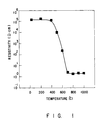
- Fig. 1 shows a property of a p-type-impurity-doped GaN series compound semiconductor, and is a graph showing the relationship between an annealing temperature and the resistance value of the GaN series compound semiconductor annealed at the temperature.
- the high-resistivity GaN series compound semiconductor can be converted into a low-resistivity p-type impurity compound semiconductor by annealing.
- the resistivity obtained by the Hall measurement on the annealed GaN series compound semiconductor is plotted as a function of the annealing temperature.
- the used GaN series compound semiconductor was formed by growing a GaN buffer layer on a sapphire substrate by the MOCVD method, followed by formation of a 4 ⁇ m-thick GaN layer on the buffer layer while doping Mg thereinto as a p-type impurity.
- the data plotted on Fig. 1 were obtained as results of annealing the substrate having these layers in a nitrogen atmosphere for 10 minutes at various temperatures using an annealing equipment.
- the resistivity of the Mg-doped GaN layer sharply dropped around the point where the temperature exceeded 400°C.
- the temperature was increased to higher than 700°C, the GaN layer exhibited a substantially constant low-resistivity p-type property, indicating the effect of annealing.
- the Hall measurement was carried out for a GaN layer before annealing and after annealing at 700°C or higher.
- the GaN layer had a resistivity of 2 ⁇ 10 5 ⁇ cm and a hole carrier density of 8 ⁇ 10 10 /cm 3 , whereas after annealing, the layer had a resistivity of 2 ⁇ cm and a hole carrier density of 2 ⁇ 10 17 /cm 3 .
- Fig. 1 shows a case of only the GaN layer, but it was confirmed that a p-type-impurity-doped Ga x Al 1-x N (0 ⁇ ⁇ ⁇ 1) also exhibits a similar result.
- the 4 ⁇ m-thick GaN layer annealed at 700°C was etched to reduce the thickness thereof to 2 ⁇ m, and the Hall measurement was performed for the GaN layer.
- Annealing of the p-type-impurity-doped GaN series compound semiconductor layer may be conducted in the reaction vessel after forming the layer, or in an annealing equipment after transferring the substrate having the compound semiconductor layer from the reaction vessel thereinto.
- the annealing may be carried out in a vacuum, or in an N 2 atmosphere, or in an inert gas atmosphere of He, Ne, Ar or the like, or an atmosphere of a mixture of these gases. Most preferably, the annealing should be performed in a nitrogen atmosphere which is pressurized to a level or higher of the decomposition pressure for the GaN compound semiconductor at the annealing temperature. With the nitrogen atmosphere pressurizing the GaN compound semiconductor, decomposition of the compound and split-off of N therefrom during annealing can be prevented.
- the decomposition pressure is about 1013 kPa (0.01 atm) at a temperature of 800°C, about 101.3 MPa (1 atm) at 1000°C, and about 1013 MPa (10 atm) at 1100°C. Consequently, the GaN series compound semiconductor is annealed at 400°C, some decomposition may occur during annealing at 400°C. If decomposition occurs, the crystallinity of the GaN compound semiconductor tends to be degraded. Therefore, as stated before, the decomposition can be prevented by maintaining a pressure of the nitrogen atmosphere no lower than the decomposition pressure at the annealing temperature.
- Fig. 2 is a graph showing the difference in crystallinity between GaN series compound semiconductors one of which annealed under a pressurized condition and the other under an atmospheric pressure condition.
- Each GaN series compound semiconductor is prepared by forming a GaN buffer layer and a Mg-doped 4 ⁇ m-thick GaN layer on sapphire substrate, and annealing at 1000°C in a nitrogen atmosphere for 20 minutes under 2027 MPa (20 atm) of a pressurized condition, or in an atmospheric pressure condition.
- the p-type GaN layers were irradiated with He-Cd laser beams from He-Cd laser beam source as an excitation light beam source, so as to measure the intensity of photoluminescence as an evaluation of the crystallinity.
- a curve 201 indicates the property of the p-type GaN layer annealed under a pressure of 2027 MPa (20 atm), and a curve 202 indicates the case of annealing at atmospheric pressure.
- a GaN layer is decomposed by heat to tend to be degraded the crystallinity.
- heat decomposition can be avoided by pressurizing the GaN layer, and thus a p-type GaN layer having a good crystallinity can be obtained.
- the GaN series compound is preferably represented by general formula Ga x Al 1-x N (where 0 ⁇ x ⁇ 1), or represented by general formula In y Ga 1-y N (where 0 ⁇ y ⁇ 1).
- a cap layer may be formed on the p-type-impurity-doped GaN series compound semiconductor layer before annealing so as to prevent decomposition of the GaN compound during annealing.
- the cap layer serves as a protective layer. If the cap layer is formed on the compound semiconductor followed by annealing the compound semiconductor at 400°C or higher, decomposition thereof can be avoided even if annealed, not only in a pressurized state, but also, a pressured-reduced condition, or atmospheric condition. Thus, a p-type GaN compound semiconductor having a low resistivity and a high crystallinity can be obtained.
- the cap layer may be formed in the reaction vessel following forming the p-type-impurity-doped GaN series compound semiconductor.
- the substrate having the GaN series compound semiconductor may be transferred from the reaction vessel into a crystal growing method such as a plasma CVD device or the like, so as to form a cap layer on the semiconductor.
- the cap layer may be made of an arbitrary material as long as it is formable on the GaN compound, and stable even at a temperature of 400°C or higher.
- Preferable examples thereof are Ga x Al 1-x N (where 0 ⁇ x ⁇ 1), Ga y In 1-y N (where 0 ⁇ y ⁇ 1), Si 3 N 4 , and SiO 2 . Which is the most preferable material depends upon the annealing temperature.
- the cap layer should have a thickness in the range of about 0.01-5 ⁇ m. If the cap layer is thinner than 0.01 ⁇ m, the advantage as a protection layer cannot be sufficiently obtained, whereas if thicker than 5 ⁇ m, it takes a lot of work to remove the layer to expose the p-type GaN series compound semiconductor after annealing, i.e., not economical. With the conventional electron beam irradiation method, GaN in the uppermost layer is decomposed, degrading the crystallinity, and therefore sufficiently bright light cannot be expected from the manufactured blue-light emitting element. However, such decomposition of GaN can be effectively prevented by the cap layer, blue-light emitting elements each having a high brightness can be manufactured at a high yield.
- the substrate may be made of, other than sapphire, SiC, Si, or the like.
- Examples of the p-type impurity are Zn, Cd, Be, Mg, Ca, and Ba.
- Fig. 3 is a graph showing comparison with regard to crystallinity between a cap-layered GaN compound semiconductor conductor and an ordinary GaN series compound having no cap layer.
- a GaN series compound semiconductor having a GaN buffer layer and a Mg-doped 4 ⁇ m-thick GaN layer formed on a substrate (curve 301) and the GaN series compound semiconductor further covered by a 0.5 ⁇ m-thick AlN layer as the cap layer (302) are compared with each other.
- Each of the semiconductors was prepared by annealing it in a nitrogen atmosphere of atmospheric pressure at 1000°C for 20 minutes, and etching the cap layer therefrom to expose the GaN series compound semiconductor. Then, the intensity of photoluminescence of each semiconductor was measured.
- the compound is decomposed greatly in high-temperature annealing (see curve 301), resulting in a low intensity of light emission at 450 nm.
- the cap-layer-formed (AlN layer) p-type GaN layer decomposition occurs only to AlN of the cap layer, and the p-type GaN layer remains; therefore the light emitting intensity is maintained as high as a level of not decomposed low sensitivity p-type GaN.
- NH 3 is generally used as an N source. During the growth, NH 3 is decomposed to atomic hydrogens. These hydrogen atoms bond to Mg, Zn, or the like doped as an acceptor impurity to prevent the p-type impurity from acting as an acceptor. Therefore, a GaN compound semiconductor into which a p-type impurity is doped exhibits a high resistivity.
- electron beams may be irradiated on the semiconductor layer while maintaining the surface temperature thereof at 600°C or higher.
- electron beam irradiation equipment for example, SEM
- SEM electron beam irradiation equipment
- the irradiation may be carried out while heating by such as a heater the p-type GaN series compound semiconductor so as to maintain the surface temperature thereof at 600°C or higher.
- the compound semiconductor may be irradiated with electron beams of an acceleration voltage in the range of 1 kV - 30 kV to maintain the surface temperature of the p-type GaN series compound semiconductor at 600°C or higher.
- Fig. 4 is a graph showing the relationship between the surface temperature of the GaN series compound semiconductor and the resistivity in the case where the compound semiconductor is treated with electron beam irradiation.
- the GaN series compound semiconductor layer employed had the structure in which a GaN buffer layer was formed on a substrate, and an Mg-doped p-type GaN layer was formed on the buffer layer.
- the p-type-impurity-doped GaN series compound semiconductor layer obtained was irradiated with electron beams having an acceleration voltage of 15 kV.
- the temperature of the heating stage was varied, and the surface temperature of the p-type GaN layer was measured by a pyrometer. The measured temperatures and corresponding resistivities are plotted in the graph shown in Fig.
- the resistivity was as high as 10 6 ⁇ cm.
- the resistivity began to decrease rapidly, and at 700°C, it was as low as 2.0 ⁇ cm.
- the resistivity was still as high as 200 ⁇ cm, and naturally, under 600°C, the resistivity was higher.
- the surface temperature of the GaN series compound semiconductor during electron beam irradiation should be in the range of 600°C -1200°C. The irradiation can be performed at over 1200°C, but this may cause high cost.
- a stable low-resistivity p-type GaN series compound semiconductor layer at a high yield.
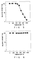
- Fig. 5 shows the relationship between the surface temperature of the p-type GaN series compound semiconductor layer during the electron beam irradiation and the intensity of photoluminescence.
- electron beam irradiation with various spot diameters is carried out so as to gradually raise the surface temperature of the p-type GaN layer.
- Fig. 5 is a graph showing the intensity of photoluminescence as a function of the surface temperature of the GaN compound.
- the intensity of blue-light emission gradually decreases.
- the reason why the intensity of the blue-light emission decreases is that the crystallinity of the semiconductor is degraded due to decomposition of GaN in the surface portion.
- a blue light-emitting element formed using a sample having such a low intensity of light emission does not emit bright light.
- the authors of the present invention found that decomposition of p-type GaN during electron beam irradiation can be prevented by providing a cap layer on the surface of the p-type GaN layer.
- the cap layer serves as a protection layer for the p-type GaN series compound semiconductor.
- the material of this cap layer is arbitrary as long as it is formable on the surface of the p-type GaN layer and fairly stable at a temperature of 600°C or higher.
- the material are Ga x Al 1-x N (0 ⁇ x ⁇ 1), In y Ga 1-y N (0 ⁇ y ⁇ 1), SiO 2 , Si 3 N 4 , etc.
- the cap layer should have a thickness in the range of about 0.01-5 ⁇ m, preferably 0.01-1 ⁇ m.
- the cap layer is thinner than 0.01 ⁇ m, the advantage as a protection layer cannot be sufficiently obtained, whereas if thicker than 5 ⁇ m, it takes a lot of work to remove the layer to expose the p-type GaN series compound semiconductor after annealing, i.e., not economical.
- Fig. 6 is a graph showing the relationship between the surface temperature of a cap-layer-provided p-type GaN series compound semiconductor, and the intensity of photoluminescence in the case where the semiconductor is treated by electron beam irradiation.
- a 0.1 ⁇ m-thick SiO 2 layer was formed on the p-type GaN compound semiconductor as a protection layer, and electron-beam irradiation was carried out to the compound semiconductor through the cap layer. Then, the cap layer was removed by etching, and the photoluminescence intensity of the exposed p-type GaN layer was measured.
- the graph shown in Fig. 6 shows the photoluminescence intensity as a function of the temperature. As is apparent from Fig. 6, the intensity of 450 nm-light emission was not deteriorated at a temperature of 600°C, proving that the cap layer acted effectively to suppress the decomposition of GaN.
- a low-resistivity p-type GaN series compound semiconductor can be obtained even in the electron beam irradiation at a temperature of 600°C or higher.
- a p-type-impurity-doped GaN series compound semiconductor exhibits a high resistivity
- hydrogen bonded to Mg or-Zn in the form of Mg-H or Zn-H is released therefrom by heat when the semiconductor is heated over 600°C, especially 700°C or higher.
- hydrogen leaves the p-type-impurity-doped GaN series compound semiconductor, and the p-type impurity such as Mg or Zn now free from hydrogen can act normally as an acceptor. Accordingly, a low-resistivity p-type GaN series compound semiconductor can be obtained.
- the second aspect of the invention is directed to a method of manufacturing a p-type Il-VI Group compound semiconductor element by a chemical vapour decomposition method, comprising the step of annealing the grown compound at a temperature of 300°C or higher.
- the annealing temperature is preferably 300°C or higher.
- the annealing step may be carried out with keeping an annealing temperature constantly for at least 1 minute, preferably 10 minutes or more.
- the annealing may be carried out in a vacuum, or in an N 2 atmosphere, or in an inert gas atmosphere of He, Ne, Ar or the like, or an atmosphere of a mixture of these gases. Most preferably, the annealing should be performed in a II Group gas atmosphere, or VI Group gas atmosphere, or an atmosphere of a mixture gas thereof which is pressurized to a level or higher of the decomposing pressure for the II-VI group compound semiconductor at the annealing temperature. If such pressured II Group gas, VI Group gas, or mixture atmosphere is used for annealing the Il-VI compound semiconductor, decomposition of the compound during annealing can be prevented.
- a cap layer may be provided on the p-type-impurity-doped Il-VI Group compound semiconductor layer so as to prevent decomposition of the compound by heat.
- the cap layer serves as a protection layer.
- the cap layer may be made of an arbitrary material as long as it is formable on the Il-VI group compound, and stable even at a temperature of 300°C or higher. Preferable examples thereof are a II-VI Group compound semiconductor, Si 3 N 4 , and SiO 2 . Which is the most preferable material depends upon the annealing temperature.
- the cap layer usually, should have a thickness in the range of about 0.01-5 ⁇ m as in the first and second aspects of the invention.
- the p-type impurity may be at least one of N, Li and O.
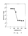
- Fig. 7 is a graph showing the relationship between the annealing temperature and the resistivity of a ZnSe compound semiconductor into which nitrogen atoms (N) are doped as a p-typed impurity.
- the ZnSe compound semiconductor layer was become a low-resistivity p-type layer by annealing.
- the ZnSe compound semiconductor used here was obtained in the following manner. A 4 ⁇ m-thick ZnSe was formed on a GaAs substrate while doping N into the layer in a stream of NH 3 as a source of a p-type impurity. In the same manner as described above some samples of ZnSe layers were obtained.
- the 4 ⁇ m-thick ZnSe layer annealed at 400°C was etched to reduce the thickness to 2 pm, and the Hall measurement was carried out.
- the hole carrier density and resistivity were 0.7 ⁇ cm, and 1 ⁇ 10 18 /cm 3 , respectively, which were substantially the same as those of the layer before the etching.
- the second aspect of the invention may further comprise the step of irradiating electron beams on the grown compound while maintaining a surface temperature of said compound at 300°C or higher.
- the surface temperature is maintained preferably at a range of temperature of 400 to 800°C or higher; however, when it exceeds 800°C, the compound semiconductor tends to be degraded.
- Electron-beam irradiation is carried out usually at a acceleration voltage of 1 kv - 30 kv, and an SEM, EPM, etc. may be used as an electron beam irradiation device.
- An N-doped ZnSe semiconductor film grown by the MOCVD method as same as above was placed in an electron beam irradiation device, and irradiated with electron beams of an acceleration voltage of 10 kV while maintaining the surface temperature at 400°C.
- the resistivity and hole carrier density of the ZnSe layer were 600 ⁇ cm, and 1 ⁇ 10 15 /cm 3 , respectively, whereas those of the layer after the irradiation were 0.8 ⁇ cm, and 1 ⁇ 10 18 /cm 3 , respectively.
- NH 3 is generally used as a source of N, which serves as a p-type dopant. During the growth, NH 3 decomposes to release atomic hydrogen. These hydrogen atoms bond to N doped as an acceptor impurity to prevent N from serving as an acceptor. Therefore, a II-VI Group compound semiconductor into which a impurity N is doped exhibits a high resistivity.
- the electron beam irradiation may be carried out at an acceleration voltage of 1 kV - 30 kV so as to achieve a low resistivity with the highest reproducibility. If the acceleration voltage is lower than 1 kV, the energy of the electron beams tends to not have a level sufficient to release hydrogen atoms, whereas if it exceeds 30 kV, the electron energy gets so large that the sample temperature is raised too high even if the emission current is low. If the sample temperature is too high, the sample itself is broken, making it difficult to control the state of the sample.
- a sapphire substrate was well washed, and placed in the susceptor in the reaction vessel. After creating a vacuum in the container, the substrate was heated at 1050°C for 20 min in a stream of hydrogen gas so as to remove an oxide present in the surface of the substrate. Then, the substrate temperature was cooled to 510°C. At a temperature of 510°C, TMG gas serving as a Ga source was introduced to the substrate at 27 ⁇ 10 -6 mol/min., and so were ammonia gas serving as an N source at 4.0 l/min., hydrogen gas serving as a carrier gas at 2.0 l/min, so as to grow a GaN buffer layer having a thickness of 20nm on the substrate.
- the supply of the TMG gas was stopped, and the substrate was again heated up to 1030°C.
- the TMG gas was again introduced at 54 ⁇ 10 -6 mol/min, and Cp 2 Mg (cyclopentadienylmagnesium) gas was newly added at 3.6 ⁇ 10 -6 mol/min for 60 min., and thus an Mg-doped GaN layer having a thickness of 4 pm was grown on the GaN buffer layer.
- the substrate now having the above-described layers was taken out of the reaction vessel, and transferred into an annealing device, where these layers were annealed in a nitrogen atmosphere at atmospheric pressure and 800°C for 20 minutes.
- a GaN buffer layer and Mg-doped GaN layer were grown as in Embodiment 1. Then, supply of the Cp 2 Mg gas was stopped, and a 0.5 ⁇ m-thick-GaN layer was grown thereon as a cap layer.
- these layers were annealed in a nitrogen/argon mixture gas at atmospheric pressure and 800°C for 20 minutes in an annealing device. Then, etching was performed on the substrate to remove the 0.5 ⁇ m-thick-cap layer from the surface portion, and thus the Mg-doped GaN layer was exposed.
- a Hall measurement was conducted on the annealed Mg-doped GaN layer as in Embodiment 1. The result indicated that the Mg-doped GaN layer exhibited good p-type characteristics, i.e., a resistivity of 2 ⁇ cm and a hole carrier density of 1.5 ⁇ 10 17 /cm 3 . Further, the intensity of blue-light emission of photoluminescence at 450 nm was about 4 times as much as that of the GaN layer obtained in Embodiment 1.
- a GaN buffer layer and Mg-doped GaN layer were grown on a substrate as in Embodiment 1. Then, the substrate was transferred from the reaction vessel to an annealing device. These layers were annealed in a nitrogen gas at a pressure of 2027 MPa (20 atm), and at a temperature of 800°C for 20 minutes in the annealing device. A Hall measurement was conducted on the annealed Mg-doped GaN layer. The result indicated that the Mg-doped GaN layer exhibited good p-type characteristics, i.e., a resistivity of 2 ⁇ cm and a hole carrier density of 2.0 ⁇ 10 17 /cm 3 . Further, the intensity of blue-light emission of photoluminescence at 450 nm was about 4 times as much as that of the GaN layer obtained in Embodiment 1.
- a GaN buffer layer and Mg-doped GaN layer were grown on a substrate as in Embodiment 1. Then, the substrate was transferred from the reaction vessel to a plasma CVD device, where a 0.5 ⁇ m-thick-SiO 2 layer serving as a cap layer was formed on the Mg-doped GaN layer.
- the substrate having these layers thereon was put in an annealing device, where these layers were annealed in a nitrogen/argon mixture gas at atmospheric pressure and 1000°C for 20 minutes. Then, the SiO 2 cap layer was removed with hydrofluoric acid to expose the Mg-doped GaN layer. A Hall measurement was conducted on the annealed and Mg-doped GaN layer. The result indicated that the Mg-doped GaN layer exhibited good p-type characteristics, i.e., a resistivity of 2 ⁇ cm and a hole carrier density of 2.0 ⁇ 10 17 /cm 3 .
- an Mg-doped GaN layer was formed on a substrate in the same manner as described above except that no cap layer was formed. It was found that the Mg-doped GaN layer, with a cap layer formed thereon while annealing, exhibited about 20 times as much intensity of blue-light emission of photoluminescence at about 450 nm as that of the Mg-doped GaN layer annealed without a cap layer formed thereon.
- a GaN buffer layer and Mg-doped GaN layer were grown on a sapphire substrate as in Embodiment 1, and then, supply of the Cp 2 Mg gas was stopped. After that, TMA gas and SiH 4 (monosilane) gas were newly introduced at 6 ⁇ 10 -16 mol/min, and 2.2 ⁇ 10 -10 mol/min, respectively, for 20 minutes so as to grow a 0.8 ⁇ m-thick Si-doped n-type Ga 0.9 Al 0.1 N layer on the Mg-doped GaN layer.
- TMA gas and SiH 4 (monosilane) gas were newly introduced at 6 ⁇ 10 -16 mol/min, and 2.2 ⁇ 10 -10 mol/min, respectively, for 20 minutes so as to grow a 0.8 ⁇ m-thick Si-doped n-type Ga 0.9 Al 0.1 N layer on the Mg-doped GaN layer.
- an element having a single hetero structure i.e., a p-type GaN layer, and an n-type Ga 0.9 Al 0.1 N layer were formed on the sapphire.
- n-type Ga 0.9 Al 0.1 N layer was etched by a general method so as to expose a part of p-type GaN layer.
- an ohmic electrode is provided for each of the layers, and the element was cut into chip-like pieces by a dicing saw. Each of the electrodes were taken out from the n-type and p-type layers exposed on each chip.
- Each chip was molded into a blue-light emitting diode.
- the obtained light-emitting diode exhibited characteristics, i.e., blue-light emission with a peak wavelength at 430 nm, an output power of 90 ⁇ W, and a forward voltage of 5V, at a forward current of 20 mA.
- the exhibited light-emitting output of the blue-light emitting diode was as high as never reported before.
- a light-emitting diode having a similar single hetero structure to that of Embodiment 5 was manufactured in a similar manner to that of Embodiment 5 except that in Control 1 annealing was not carried out.
- the obtained light-emitting diode exhibited a forward voltage of as high as 60V for a forward current of 20 mA. A slight yellow-like color light emission was generated, but the diode was broken as soon as it was turned on. Thus, the light emission output could not be measured.
- a 20nm-thick GaN buffer layer was grown on a sapphire substrate as in Embodiment 1.
- TMG gas was introduced at 54 ⁇ 10 -6 mol/min, and SiH 4 (monosilane) gas was newly introduced at 2.2 ⁇ 10 -10 mol/min, for 60 minutes so as to grow a 4 ⁇ m-thick Si-doped n-type GaN layer on the GaN buffer layer.
- a light-emitting diode was made from the element so obtained as in Embodiment 4, and the light-emitting diode was turned on.
- the diode generated blue light with a light emission peak at 430 nm, and exhibited characteristics, i.e., an output power of 50 ⁇ W at 20 mA and a forward voltage of 4V at 20 mA.
- a light-emitting diode having a similar homo GaN structure was manufactured in a similar manner to that of Embodiment 6 except that annealing was not carried out.
- the obtained light-emitting diode exhibited a forward voltage of as high as 40V at a forward direction current of 20 mA.
- a slight yellow-like color light emission was generated, but the diode was broken as soon as it was turned on. Thus, the light emission output could not be measured.
- a GaN buffer layer having a thickness of 250 ⁇ was grown on a substrate.
- the temperature of the substrate was again raised up to 1030°C.
- the TMG gas was again introduced at 54 ⁇ 10 -6 mol/min, and Cp 2 Mg (cyclopentadienylmagnesium) gas was newly introduced at 3.6 ⁇ 10 -6 mol/min for 60 min., and thus an Mg-doped GaN layer having a thickness of 4 ⁇ m was grown on the GaN buffer layer.
- the substrate now having the above-described layers was taken out of the reaction vessel, and transferred into an electron beam irradiation device, where these layers were irradiated with electron beams having an acceleration voltage of 15 kV while maintaining the surface temperature of the GaN layer at 800°C by a heater.
- the Hall measurement was conducted on the electron-beam-irradiated Mg-doped GaN layer.
- a GaN buffer layer and Mg-doped GaN layer were grown as in Embodiment 7. Then, supply of the Cp 2 Mg gas was stopped, and a 0.1 ⁇ m-thick-GaN layer was grown thereon as a cap layer.
- these layers were irradiated with electron beams in the electron beam irradiation device while maintaining the surface temperature of the GaN layer at 800°C. Then, etching was performed to remove the 0.1 ⁇ m-thick-cap layer from the surface portion, and thus the Mg-doped GaN layer was exposed.
- a Hall measurement was conducted on the Mg-doped GaN layer so obtained as in Embodiment 1. The result indicated that the Mg-doped GaN layer had good p-type characteristics including a resistivity of 2 ⁇ cm. Further, the intensity of blue-light emission of photoluminescence at 450 nm was about 4 times as high as that of the GaN layer obtained in Embodiment 1.
- An Mg-doped GaN layer was grown on a substrate as in Embodiment 7. Then, the substrate was transferred from the reaction vessel to a plasma CVD device, where a 0.2 ⁇ m-thick SiO 2 layer was formed thereon as a cap layer.
- the SiO 2 cap layer was removed with hydrofluoric acid to expose the Mg-doped GaN layer.
- a Hall measurement was conducted on the Mg-doped GaN layer so obtained. The result indicated that the Mg-doped GaN layer had good p-type characteristics, i.e., a resistivity of as low as 2 ⁇ cm and a hole carrier density of 2.0 ⁇ 10 17 /cm 3 . Further, the photoluminescence intensity at 450 nm was about 4 times as high as that obtained in Embodiment 7.
- an Mg-doped GaN layer was grown on a substrate in a reaction vessel, and the substrate was transferred into a plasma CVD device, where a 0.5 ⁇ m-thick Si 3 O 4 layer was formed on the grown layer as a cap layer.
- the obtained layers were irradiated with electron beams having an acceleration voltage of 15 kV while maintaining the surface temperature of the GaN layer at 1000°C by a heater. Then, the Si 3 N 4 layer was removed by etching to expose the Mg-doped GaN layer. The Hall measurement was conducted on the electron-beam-irradiated Mg-doped GaN layer. The results indicated that the Mg-doped GaN layer so obtained had good p-type characteristics, i.e., a resistivity of 2 ⁇ cm and a hole carrier density of 2 ⁇ 10 17 /cm 3 .
- an Mg-doped GaN layer was formed on a substrate in the same manner as described above except that no cap layer was formed. It was found that the Mg-doped GaN layer with a cap layer formed thereon had about 15 times as high intensity of blue-light emission of photoluminescence at 450 nm as that of the Mg-doped GaN layer without a cap layer.
- a 25nm-thick GaN buffer layer was grown on a sapphire substrate as in Embodiment 7.
- TMG gas was introduced at 54 ⁇ 10 -6 mol/min, and SiH 4 (monosilane) gas was newly added at 2.2 ⁇ 10 -10 mol/min, for 60 minutes so as to grow a 4 ⁇ m-thick Si-doped n-type GaN layer on the buffer layer.
- the cap layer was removed by dipping it into hydrofluoric acid, and a part of the p-type GaN layer of the element obtained was etched so as to expose a part of n-type GaN layer. Then, an ohmic electrode is provided for each of the layers, and the element was cut into chip-like pieces by a dicing saw. Each of the electrodes were taken out from the n-type and p-type layers exposed on each chip. Each chip was molded into a blue-light-emitting diode.
- the obtained light-emitting diode exhibited characteristics, i.e., blue-light emission with a peak wavelength at 430 nm, an output power of 50 ⁇ W at 20 mA, and a forward voltage of 4V at 20 mA.
- a GaAs substrate was well washed, and placed in the susceptor in the reaction vessel. After creating a vacuum in the container, the substrate was heated at 600°C for 10 min. in a stream of hydrogen gas so as to remove the oxidized surface portion of the substrate. Then, the substrate temperature was lowered to 350°C.
- the substrate having the layers thereon was taken out of the reaction vessel, and transferred into an annealing device, where these layers were annealed in a nitrogen atmosphere at atmospheric pressure and 400°C for 20 minutes.
- a Hall measurement was conducted on the annealed and N-doped ZnSe layer. The result indicated that the N-doped ZnSe layer had good p-type characteristics, i.e., a resistivity of 0.8 ⁇ cm and a hole carrier density of 1 ⁇ 10 18 /cm 3 .
- a GaAs substrate having a N-doped ZnSe layer grown thereon as in Embodiment 12 in a reaction vessel was transferred into an electron beam irradiation device, where electron beam irradiation was carried out to the grown N-doped ZnSe layer at an acceleration of 10 kV.
- a Hall measurement was conducted on the obtained N-doped ZnSe layer. The results indicated that the N-doped ZnSe layer had good p-type characteristics, i.e., a resistivity of as low as 0.7 ⁇ cm and a hole carrier density of 1 ⁇ 10 18 /cm 3 .
- An N-doped ZnSe layer was grown on a GaAs substrate as in Embodiment 12, and then a 0.1 ⁇ m-thick ZnSe layer was grown thereon as a cap layer.
- the substrate obtained was annealed in an annealing device. Then, the surface portion corresponding to a 0.1 ⁇ m-thick layer was stripped by etching to remove the cap layer, thereby exposing the N-doped ZnSe layer. A Hall measurement was conducted on the obtained N-doped ZnSe layer. The result indicated that the N-doped ZnSe layer exhibited good p-type characteristics, i.e., a resistivity of 0.6 ⁇ cm and a hole carrier density of 3 ⁇ 10 18 /cm 3 .
- N-doped ZnSe layer was grown on a GaAs substrate as in Embodiment 12, and the substrate obtained was transferred from the reaction vessel to a plasma CVD device, where a 0.2 ⁇ m-thick-SiO 2 layer serving as a cap layer was formed on the N-doped ZnSe layer.
Description
Although the foregoing describes embodiments of GaxAℓ1-xN (where 0 ≦ x ≦ 1) compound semiconductors, a III-V Group compound semiconductor according to the present invention is not limited to GaxAℓ1-xN and a InyGa1-yN can also be used.
Claims (25)
- A method of manufacturing a p-type gallium nitride semiconductor element by a vapour phase epitaxy method comprising the step of growing a gallium compound on a support, said support comprising at least a substrate, by using a reaction gas, the reaction gas containing a p-type impurity and a source of hydrogen atoms, the hydrogen atoms being released from the source and bonding to the p-type impurity, characterised in that the compound is annealed after growth at a temperature of 400°C or higher.
- A method according to claim 1, characterised in that said gallium compound is represented by the general formula GaxAl1-xN (where O ≤ x ≤ 1).
- A method according to claim 1 or 2, characterised in that the compound is annealed at a temperature in the range of 600°C-1200°C.
- A method according to claim 1,2 or 3, characterised in that a cap layer is provided on said gallium compound before annealing.
- A method according to claim 4, characterised in that said cap layer is made of at least one material selected from GaxAl1-xN (wherein O ≤ x ≤ 1), InyGa1-yN (where 0 ≤ y ≤1), AlN, Si3N and SiO2.
- A method according to any preceding claim, characterised in that said annealing is carried out in a nitrogen atmosphere pressurized to the decomposition pressure of the gallium compound at said annealing temperature, or higher.
- A method according to any preceding claim, wherein the support comprises only a substrate, and the gallium compound is grown directly on the substrate.
- A method according to any one of claims 1 to 6, wherein the support comprises a substrate and a buffer layer grown on the substrate, and wherein the gallium compound is grown directly on the buffer layer.
- A method according to claim 8, characterised in that said buffer layer is made of GaN.
- A method according to claim 7,8 or 9, characterised in that the substrate is made of at least one material selected from sapphire, SiC, GaAs and Si.
- A method according to any preceding claim, characterised in that said reaction gas contains at least one of a gallium source selected from trimethyl gallium and diethyl gallium, and an aluminium source selected from trimethyl aluminium and diethyl aluminium, an indium source selected from trimethyl indium and diethyl indium, and a nitrogen source selected from ammonia and hydrazin.
- A method according to any preceding claim, characterised in that said p-type impurity is at least one of Zn, Cd, Be, Mg, Ca and Ba.
- A method according to any preceding claim, characterised in that the gallium compound is irradiated with electron beams while maintaining the surface temperature of the compound at 600°C or higher.
- A method according to claim 13, characterised in that an acceleration voltage is controlled within a range of 1 kV - 30 kV in said electron beam irradiation step.
- A method according to claim 13 or 14, characterised in that the surface temperature of the gallium compound is maintained in the range of 600°C-1200°C.
- A method of manufacturing a p-type II-VI Group compound semiconductor element by a chemical vapour deposition method comprising the step of growing a II-VI Group compound on a substrate by using a reaction gas, wherein the reaction gas contains a p-type impurity and a source of hydrogen atoms, the hydrogen atoms being released from the source and bonding to the p-type impurity, and the compound is annealed after growth at a temperature of 300°C or higher.
- A method according to claim 16, characterised in that the compound is annealed at a temperature in the range of 400°C-1200°C.
- A method according to claim 16 or 17, characterised in that the annealing is carried out in an atmosphere of a II group gas, a VI group gas, or a mixture thereof, pressurized to the decomposition pressure of the II-VI group compound at said annealing temperature, or higher.
- A method according to claim 16,17 or 18, characterised by further comprising the step of forming a cap layer on said compound before annealing.
- A method according to claim 19, characterised in that said cap layer is made of at least one material selected from a II-VI compound semiconductor, Si3N4 and SiO2.
- A method according to any of claims 16 to 20, characterised in that the II-VI Group compound is grown on a substrate, which substrate is made of at least one material selected from GaAs, ZnSe, GaP and InP.
- A method according to any of claims 16 to 21, characterised in that the reaction gas contains at least one of a II group element source selected from diethyl zinc, diethyl cadmium and diethyl magnesium, and a VI group source selected from hydrogen selenide and hydrogen sulphide.
- A method according to any of claims 16 to 22, characterised in that said p-type impurity is at least one of N, Li and O.
- A method according to any of claims 16 to 23, characterised in that the II-VI Group compound is irradiated with electron beams while maintaining the surface temperature of the compound at 300°C or higher.
- A method according to claim 24, characterised in that the surface temperature of the II-VI Group compound is maintained in the range of 300°C-1200°C in the electron beam irradiating step.
Applications Claiming Priority (12)
| Application Number | Priority Date | Filing Date | Title |
|---|---|---|---|
| JP32135391 | 1991-11-08 | ||
| JP32135391 | 1991-11-08 | ||
| JP321353/91 | 1991-11-08 | ||
| JP35704691A JP2540791B2 (en) | 1991-11-08 | 1991-12-24 | A method for manufacturing a p-type gallium nitride-based compound semiconductor. |
| JP357046/91 | 1991-12-24 | ||
| JP35704691 | 1991-12-24 | ||
| JP3276392A JPH05198841A (en) | 1992-01-22 | 1992-01-22 | Forming method for p-type of gallium nitride compound semiconductor |
| JP32763/92 | 1992-01-22 | ||
| JP3276392 | 1992-01-22 | ||
| JP4028092 | 1992-01-29 | ||
| JP4028092A JPH05206520A (en) | 1992-01-29 | 1992-01-29 | Manufacture of p-type ii-vi compound semiconductor |
| JP40280/92 | 1992-01-29 |
Publications (4)
| Publication Number | Publication Date |
|---|---|
| EP0541373A2 EP0541373A2 (en) | 1993-05-12 |
| EP0541373A3 EP0541373A3 (en) | 1993-07-28 |
| EP0541373B1 true EP0541373B1 (en) | 1998-09-30 |
| EP0541373B2 EP0541373B2 (en) | 2004-03-31 |
Family
ID=27459676
Family Applications (1)
| Application Number | Title | Priority Date | Filing Date |
|---|---|---|---|
| EP92310132A Expired - Lifetime EP0541373B2 (en) | 1991-11-08 | 1992-11-05 | Method of manufacturing p-type compound semiconductor |
Country Status (3)
| Country | Link |
|---|---|
| US (2) | US5306662A (en) |
| EP (1) | EP0541373B2 (en) |
| DE (1) | DE69227170T3 (en) |
Cited By (1)
| Publication number | Priority date | Publication date | Assignee | Title |
|---|---|---|---|---|
| US6996150B1 (en) | 1994-09-14 | 2006-02-07 | Rohm Co., Ltd. | Semiconductor light emitting device and manufacturing method therefor |
Families Citing this family (216)
| Publication number | Priority date | Publication date | Assignee | Title |
|---|---|---|---|---|
| US5633192A (en) * | 1991-03-18 | 1997-05-27 | Boston University | Method for epitaxially growing gallium nitride layers |
| JP3098773B2 (en) * | 1991-03-18 | 2000-10-16 | トラスティーズ・オブ・ボストン・ユニバーシティ | Preparation and doping method of highly insulating single crystal gallium nitride thin film |
| US7235819B2 (en) * | 1991-03-18 | 2007-06-26 | The Trustees Of Boston University | Semiconductor device having group III nitride buffer layer and growth layers |
| JP2540791B2 (en) * | 1991-11-08 | 1996-10-09 | 日亜化学工業株式会社 | A method for manufacturing a p-type gallium nitride-based compound semiconductor. |
| US5724062A (en) * | 1992-08-05 | 1998-03-03 | Cree Research, Inc. | High resolution, high brightness light emitting diode display and method and producing the same |
| KR100286699B1 (en) | 1993-01-28 | 2001-04-16 | 오가와 에이지 | Gallium Nitride Group 3-5 Compound Semiconductor Light-Emitting Device and Manufacturing Method Thereof |
| US5547897A (en) * | 1993-07-14 | 1996-08-20 | Philips Electronics North America Corporation | Photo-assisted nitrogen doping of II-VI semiconductor compounds during epitaxial growth using an amine |
| US5657335A (en) * | 1993-11-01 | 1997-08-12 | The Regents, University Of California | P-type gallium nitride |
| JPH07263748A (en) * | 1994-03-22 | 1995-10-13 | Toyoda Gosei Co Ltd | Iii group nitride semiconductor light emitting element and manufacture of it |
| JPH07273366A (en) * | 1994-03-28 | 1995-10-20 | Pioneer Electron Corp | Manufacture of light-emitting device made of nitride of group iii element |
| US5419785A (en) * | 1994-04-12 | 1995-05-30 | The United States Of America As Represented By The Secretary Of The Navy | Intrinsically doped III-A and V-A compounds having precipitates of V-A element |
| US5604763A (en) * | 1994-04-20 | 1997-02-18 | Toyoda Gosei Co., Ltd. | Group III nitride compound semiconductor laser diode and method for producing same |
| US5814533A (en) * | 1994-08-09 | 1998-09-29 | Rohm Co., Ltd. | Semiconductor light emitting element and manufacturing method therefor |
| US5604135A (en) * | 1994-08-12 | 1997-02-18 | Cree Research, Inc. | Method of forming green light emitting diode in silicon carbide |
| US5523589A (en) * | 1994-09-20 | 1996-06-04 | Cree Research, Inc. | Vertical geometry light emitting diode with group III nitride active layer and extended lifetime |
| US5592501A (en) * | 1994-09-20 | 1997-01-07 | Cree Research, Inc. | Low-strain laser structures with group III nitride active layers |
| JP3369816B2 (en) * | 1994-11-29 | 2003-01-20 | 三洋電機株式会社 | Method for manufacturing p-type semiconductor crystal |
| US5843590A (en) * | 1994-12-26 | 1998-12-01 | Sumitomo Electric Industries, Ltd. | Epitaxial wafer and method of preparing the same |
| JPH08222797A (en) * | 1995-01-17 | 1996-08-30 | Hewlett Packard Co <Hp> | Semiconductor device and manufacture thereof |
| US5656538A (en) * | 1995-03-24 | 1997-08-12 | The Board Of Trustees Of The University Of Illinois | Halide dopant process for producing semi-insulating group III-V regions for semiconductor devices |
| US6617235B2 (en) | 1995-03-30 | 2003-09-09 | Sumitomo Chemical Company, Limited | Method of manufacturing Group III-V compound semiconductor |
| US5739554A (en) * | 1995-05-08 | 1998-04-14 | Cree Research, Inc. | Double heterojunction light emitting diode with gallium nitride active layer |
| JP3771952B2 (en) * | 1995-06-28 | 2006-05-10 | ソニー株式会社 | Method for growing single crystal III-V compound semiconductor layer, method for manufacturing light emitting element, and method for manufacturing transistor |
| US5677538A (en) * | 1995-07-07 | 1997-10-14 | Trustees Of Boston University | Photodetectors using III-V nitrides |
| DE19680872B4 (en) * | 1995-08-31 | 2009-01-08 | Kabushiki Kaisha Toshiba, Kawasaki | Method for producing a light-emitting element |
| US7385574B1 (en) | 1995-12-29 | 2008-06-10 | Cree, Inc. | True color flat panel display module |
| US5812105A (en) * | 1996-06-10 | 1998-09-22 | Cree Research, Inc. | Led dot matrix drive method and apparatus |
| US5786233A (en) * | 1996-02-20 | 1998-07-28 | U.S. Philips Corporation | Photo-assisted annealing process for activation of acceptors in semiconductor compound layers |
| US6600175B1 (en) | 1996-03-26 | 2003-07-29 | Advanced Technology Materials, Inc. | Solid state white light emitter and display using same |
| US6403708B2 (en) | 1996-05-27 | 2002-06-11 | Mitsui Chemicals Inc | Crystalline polypropylenes, process for preparing thereof, polypropylene compositions, and thermoformed products |
| JP3711635B2 (en) * | 1996-06-17 | 2005-11-02 | ソニー株式会社 | Method for growing nitride III-V compound semiconductor |
| US5776793A (en) * | 1996-06-27 | 1998-07-07 | National Science Council | Method of fabricating opto-electronic device |
| TW383508B (en) | 1996-07-29 | 2000-03-01 | Nichia Kagaku Kogyo Kk | Light emitting device and display |
| US5834331A (en) * | 1996-10-17 | 1998-11-10 | Northwestern University | Method for making III-Nitride laser and detection device |
| US6291840B1 (en) | 1996-11-29 | 2001-09-18 | Toyoda Gosei Co., Ltd. | GaN related compound semiconductor light-emitting device |
| CN100485984C (en) | 1997-01-09 | 2009-05-06 | 日亚化学工业株式会社 | Nitride semiconductor device |
| US6677619B1 (en) * | 1997-01-09 | 2004-01-13 | Nichia Chemical Industries, Ltd. | Nitride semiconductor device |
| EP1024479B1 (en) * | 1997-01-17 | 2002-11-06 | Matsushita Electric Industrial Co., Ltd. | Optical pickup and optical disk apparatus using the same |
| US6333522B1 (en) | 1997-01-31 | 2001-12-25 | Matsushita Electric Industrial Co., Ltd. | Light-emitting element, semiconductor light-emitting device, and manufacturing methods therefor |
| US6284395B1 (en) | 1997-03-05 | 2001-09-04 | Corning Applied Technologies Corp. | Nitride based semiconductors and devices |
| TW329058B (en) * | 1997-03-20 | 1998-04-01 | Ind Tech Res Inst | Manufacturing method for P type gallium nitride |
| JPH10326941A (en) * | 1997-03-27 | 1998-12-08 | Sony Corp | Semiconductor light-emitting element, manufacture thereof and optical device |
| JPH10294490A (en) * | 1997-04-17 | 1998-11-04 | Toshiba Electron Eng Corp | P-type gallium nitride compound semiconductor, manufacture thereof, and blue light-emitting element |
| PL183687B1 (en) | 1997-06-06 | 2002-06-28 | Centrum Badan | Method of obtaining semiconductive compounds of a3-b5 group and electric conductivity of p and n type |
| US5888886A (en) * | 1997-06-30 | 1999-03-30 | Sdl, Inc. | Method of doping gan layers p-type for device fabrication |
| AU747260B2 (en) | 1997-07-25 | 2002-05-09 | Nichia Chemical Industries, Ltd. | Nitride semiconductor device |
| US5926726A (en) * | 1997-09-12 | 1999-07-20 | Sdl, Inc. | In-situ acceptor activation in group III-v nitride compound semiconductors |
| US6599133B2 (en) | 1997-11-18 | 2003-07-29 | Technologies And Devices International, Inc. | Method for growing III-V compound semiconductor structures with an integral non-continuous quantum dot layer utilizing HVPE techniques |
| US6890809B2 (en) * | 1997-11-18 | 2005-05-10 | Technologies And Deviles International, Inc. | Method for fabricating a P-N heterojunction device utilizing HVPE grown III-V compound layers and resultant device |
| US6479839B2 (en) | 1997-11-18 | 2002-11-12 | Technologies & Devices International, Inc. | III-V compounds semiconductor device with an AlxByInzGa1-x-y-zN non continuous quantum dot layer |
| US6555452B2 (en) | 1997-11-18 | 2003-04-29 | Technologies And Devices International, Inc. | Method for growing p-type III-V compound material utilizing HVPE techniques |
| US6476420B2 (en) | 1997-11-18 | 2002-11-05 | Technologies And Devices International, Inc. | P-N homojunction-based structures utilizing HVPE growth III-V compound layers |
| US20020047135A1 (en) * | 1997-11-18 | 2002-04-25 | Nikolaev Audrey E. | P-N junction-based structures utilizing HVPE grown III-V compound layers |
| US6849862B2 (en) * | 1997-11-18 | 2005-02-01 | Technologies And Devices International, Inc. | III-V compound semiconductor device with an AlxByInzGa1-x-y-zN1-a-bPaAsb non-continuous quantum dot layer |
| US6472300B2 (en) | 1997-11-18 | 2002-10-29 | Technologies And Devices International, Inc. | Method for growing p-n homojunction-based structures utilizing HVPE techniques |
| US6559038B2 (en) | 1997-11-18 | 2003-05-06 | Technologies And Devices International, Inc. | Method for growing p-n heterojunction-based structures utilizing HVPE techniques |
| US6218269B1 (en) | 1997-11-18 | 2001-04-17 | Technology And Devices International, Inc. | Process for producing III-V nitride pn junctions and p-i-n junctions |
| US6559467B2 (en) | 1997-11-18 | 2003-05-06 | Technologies And Devices International, Inc. | P-n heterojunction-based structures utilizing HVPE grown III-V compound layers |
| US7384479B2 (en) | 1998-04-13 | 2008-06-10 | Ricoh Company, Ltd. | Laser diode having an active layer containing N and operable in a 0.6 μm wavelength |
| US6563851B1 (en) * | 1998-04-13 | 2003-05-13 | Ricoh Company, Ltd. | Laser diode having an active layer containing N and operable in a 0.6 μm wavelength band |
| US6459100B1 (en) * | 1998-09-16 | 2002-10-01 | Cree, Inc. | Vertical geometry ingan LED |
| JP3770014B2 (en) | 1999-02-09 | 2006-04-26 | 日亜化学工業株式会社 | Nitride semiconductor device |
| DE60043536D1 (en) * | 1999-03-04 | 2010-01-28 | Nichia Corp | NITRIDHALBLEITERLASERELEMENT |
| US6566256B1 (en) | 1999-04-16 | 2003-05-20 | Gbl Technologies, Inc. | Dual process semiconductor heterostructures and methods |
| DE19920871B4 (en) * | 1999-05-06 | 2004-07-01 | Steag Rtp Systems Gmbh | Process for activating charge carriers by radiation-assisted heat treatment |
| US6489225B1 (en) * | 1999-06-11 | 2002-12-03 | Electron Vision Corporation | Method for controlling dopant profiles and dopant activation by electron beam processing |
| JP4126812B2 (en) * | 1999-07-07 | 2008-07-30 | 富士ゼロックス株式会社 | Optical semiconductor device |
| US6569765B1 (en) * | 1999-08-26 | 2003-05-27 | Cbl Technologies, Inc | Hybrid deposition system and methods |
| GB2354108B (en) * | 1999-09-08 | 2001-08-08 | Arima Optoelectronics Corp | An isoelectronic co-doping method |
| US6398867B1 (en) | 1999-10-06 | 2002-06-04 | General Electric Company | Crystalline gallium nitride and method for forming crystalline gallium nitride |
| US6294016B1 (en) * | 1999-10-20 | 2001-09-25 | Kwangju Institute Of Science And Technology | Method for manufacturing p-type GaN based thin film using nitridation |
| US6441393B2 (en) * | 1999-11-17 | 2002-08-27 | Lumileds Lighting U.S., Llc | Semiconductor devices with selectively doped III-V nitride layers |
| TW449931B (en) | 2000-01-27 | 2001-08-11 | United Epitaxy Co Ltd | Manufacturing method of P-type semiconductor with a low resistance coefficient |
| EP1130659A1 (en) * | 2000-03-03 | 2001-09-05 | United Epitaxy Company, Ltd. | Method of manufacturing low resistivity p-type compound semiconductor material |
| TW440966B (en) * | 2000-03-10 | 2001-06-16 | Advanced Epitaxy Technology In | Manufacturing method to activate high resistivity p-type gallium nitride thin film into low resistivity p-type gallium nitride thin film |
| GB2361480B (en) | 2000-04-19 | 2002-06-19 | Murata Manufacturing Co | Method for forming p-type semiconductor film and light emitting device using the same |
| JP4227315B2 (en) * | 2000-04-27 | 2009-02-18 | 三星コーニング精密琉璃株式会社 | Method for manufacturing gallium nitride single crystal substrate |
| JP4581198B2 (en) | 2000-08-10 | 2010-11-17 | ソニー株式会社 | Heat treatment method for nitride compound semiconductor layer and method for manufacturing semiconductor device |
| TW478182B (en) | 2000-11-09 | 2002-03-01 | United Epitaxy Co Ltd | Fabrication of light-emitting device |
| AU2002235146A1 (en) | 2000-11-30 | 2002-06-11 | North Carolina State University | Non-thermionic sputter material transport device, methods of use, and materials produced thereby |
| AU2002219966A1 (en) | 2000-11-30 | 2002-06-11 | North Carolina State University | Methods and apparatus for producing m'n based materials |
| EP1251331B1 (en) | 2001-04-18 | 2012-03-07 | Leica Geosystems AG | Geodetic measuring device |
| US6653166B2 (en) * | 2001-05-09 | 2003-11-25 | Nsc-Nanosemiconductor Gmbh | Semiconductor device and method of making same |
| US6784074B2 (en) | 2001-05-09 | 2004-08-31 | Nsc-Nanosemiconductor Gmbh | Defect-free semiconductor templates for epitaxial growth and method of making same |
| US6479313B1 (en) | 2001-05-25 | 2002-11-12 | Kopin Corporation | Method of manufacturing GaN-based p-type compound semiconductors and light emitting diodes |
| AU2002328130B2 (en) * | 2001-06-06 | 2008-05-29 | Ammono Sp. Z O.O. | Process and apparatus for obtaining bulk monocrystalline gallium-containing nitride |
| US6537838B2 (en) | 2001-06-11 | 2003-03-25 | Limileds Lighting, U.S., Llc | Forming semiconductor structures including activated acceptors in buried p-type III-V layers |
| US6929831B2 (en) * | 2001-09-15 | 2005-08-16 | Trikon Holdings Limited | Methods of forming nitride films |
| KR100679387B1 (en) * | 2001-10-26 | 2007-02-05 | 암모노 에스피. 제트오. 오. | Nitride semiconductor laser devise and manufacturing method thereof |
| US6881983B2 (en) * | 2002-02-25 | 2005-04-19 | Kopin Corporation | Efficient light emitting diodes and lasers |
| US8809867B2 (en) * | 2002-04-15 | 2014-08-19 | The Regents Of The University Of California | Dislocation reduction in non-polar III-nitride thin films |
| KR101288489B1 (en) * | 2002-04-15 | 2013-07-26 | 더 리전츠 오브 더 유니버시티 오브 캘리포니아 | Non-polar (Al,B,In,Ga)N Quantum Well and Heterostructure Materials and Devices |
| US6911079B2 (en) * | 2002-04-19 | 2005-06-28 | Kopin Corporation | Method for reducing the resistivity of p-type II-VI and III-V semiconductors |
| AU2003229094B2 (en) * | 2002-05-17 | 2009-02-26 | Gallium Enterprises Pty Ltd | Process for manufacturing a gallium rich gallium nitride film |
| US20060138431A1 (en) * | 2002-05-17 | 2006-06-29 | Robert Dwilinski | Light emitting device structure having nitride bulk single crystal layer |
| AUPS240402A0 (en) * | 2002-05-17 | 2002-06-13 | Macquarie Research Limited | Gallium nitride |
| AU2002354467A1 (en) * | 2002-05-17 | 2003-12-02 | Ammono Sp.Zo.O. | Light emitting element structure having nitride bulk single crystal layer |
| US7002180B2 (en) * | 2002-06-28 | 2006-02-21 | Kopin Corporation | Bonding pad for gallium nitride-based light-emitting device |
| TW200400608A (en) | 2002-06-17 | 2004-01-01 | Kopin Corp | Bonding pad for gallium nitride-based light-emitting device |
| US6734091B2 (en) | 2002-06-28 | 2004-05-11 | Kopin Corporation | Electrode for p-type gallium nitride-based semiconductors |
| US6887736B2 (en) * | 2002-06-24 | 2005-05-03 | Cermet, Inc. | Method of forming a p-type group II-VI semiconductor crystal layer on a substrate |
| US6955985B2 (en) | 2002-06-28 | 2005-10-18 | Kopin Corporation | Domain epitaxy for thin film growth |
| JP2004134750A (en) * | 2002-09-19 | 2004-04-30 | Toyoda Gosei Co Ltd | Manufacturing method of p-type group iii nitride compound semiconductor |
| KR100519753B1 (en) * | 2002-11-15 | 2005-10-07 | 삼성전기주식회사 | Method for manufacturing light emitting device comprising compound semiconductor of GaN group |
| NL1022021C2 (en) * | 2002-11-28 | 2004-06-02 | Univ Eindhoven Tech | Formation of vacancies in semiconductor, useful for LEDs or laser diodes, by depositing dielectric layer on gallium arsenide structure, heating and removing this layer |
| EP1576210B1 (en) * | 2002-12-11 | 2010-02-10 | AMMONO Sp. z o.o. | A substrate for epitaxy and a method of preparing the same |
| TWI334890B (en) * | 2002-12-11 | 2010-12-21 | Ammono Sp Zoo | Process for obtaining bulk mono-crystalline gallium-containing nitride, eliminating impurities from the obtained crystal and manufacturing substrates made of bulk mono-crystalline gallium-containing nitride |
| US7122841B2 (en) | 2003-06-04 | 2006-10-17 | Kopin Corporation | Bonding pad for gallium nitride-based light-emitting devices |
| US7601553B2 (en) * | 2003-07-18 | 2009-10-13 | Epivalley Co., Ltd. | Method of manufacturing a gallium nitride semiconductor light emitting device |
| WO2005022655A1 (en) * | 2003-09-03 | 2005-03-10 | Epivalley Co., Ltd. | Algainn based optical device and fabrication method thereof |
| DE10344986B4 (en) * | 2003-09-27 | 2008-10-23 | Forschungszentrum Dresden - Rossendorf E.V. | Method of producing improved heteroepitaxial grown silicon carbide layers on silicon substrates |
| JP3833227B2 (en) * | 2003-11-04 | 2006-10-11 | 昭和電工株式会社 | Group III nitride p-type semiconductor manufacturing method and group III nitride semiconductor light emitting device |
| US20050179042A1 (en) * | 2004-02-13 | 2005-08-18 | Kopin Corporation | Monolithic integration and enhanced light extraction in gallium nitride-based light-emitting devices |
| US20050179046A1 (en) * | 2004-02-13 | 2005-08-18 | Kopin Corporation | P-type electrodes in gallium nitride-based light-emitting devices |
| JP4901115B2 (en) * | 2004-03-04 | 2012-03-21 | 昭和電工株式会社 | Gallium nitride semiconductor device |
| KR100486614B1 (en) * | 2004-03-05 | 2005-05-03 | 에피밸리 주식회사 | Ⅲ-Nitride compound semiconductor light emitting device with low contact resistance |
| KR100486177B1 (en) * | 2004-03-25 | 2005-05-06 | 에피밸리 주식회사 | Ⅲ-Nitride Compound Semiconductor Light Emitting Device |
| US7439609B2 (en) * | 2004-03-29 | 2008-10-21 | Cree, Inc. | Doping of gallium nitride by solid source diffusion and resulting gallium nitride structures |
| KR100568298B1 (en) * | 2004-03-30 | 2006-04-05 | 삼성전기주식회사 | Nitride based semiconductor having improved external quantum efficiency and fabrication method thereof |
| US7956360B2 (en) * | 2004-06-03 | 2011-06-07 | The Regents Of The University Of California | Growth of planar reduced dislocation density M-plane gallium nitride by hydride vapor phase epitaxy |
| WO2005121415A1 (en) * | 2004-06-11 | 2005-12-22 | Ammono Sp. Z O.O. | Bulk mono-crystalline gallium-containing nitride and its application |
| US20070111372A1 (en) * | 2004-07-20 | 2007-05-17 | Cermet, Inc. | Methods of forming a p-type group ii-vi semiconductor crystal layer on a substrate |
| US20060054919A1 (en) * | 2004-08-27 | 2006-03-16 | Kyocera Corporation | Light-emitting element, method for manufacturing the same and lighting equipment using the same |
| PL371405A1 (en) * | 2004-11-26 | 2006-05-29 | Ammono Sp.Z O.O. | Method for manufacture of volumetric monocrystals by their growth on crystal nucleus |
| US7253451B2 (en) * | 2004-11-29 | 2007-08-07 | Epivalley Co., Ltd. | III-nitride semiconductor light emitting device |
| JP2008528420A (en) * | 2005-01-26 | 2008-07-31 | アポロ ダイヤモンド,インク | Gallium nitride light-emitting devices on diamond |
| US7585792B2 (en) * | 2005-02-09 | 2009-09-08 | S.O.I.Tec Silicon On Insulator Technologies | Relaxation of a strained layer using a molten layer |
| KR100565894B1 (en) * | 2005-07-06 | 2006-03-31 | (주)룩셀런트 | Method of controlling active layer of iii-nitride semiconductor light emitting device |
| US20070026658A1 (en) * | 2005-08-01 | 2007-02-01 | Chia-Ming Lee | Process of forming an as-grown active p-type III-V nitride compound |
| KR20070035660A (en) * | 2005-09-28 | 2007-04-02 | 엘지이노텍 주식회사 | Fabrication method nitride semiconductor light emitting device |
| WO2007040295A1 (en) * | 2005-10-04 | 2007-04-12 | Seoul Opto Device Co., Ltd. | (al, ga, in)n-based compound semiconductor and method of fabricating the same |
| US7723154B1 (en) | 2005-10-19 | 2010-05-25 | North Carolina State University | Methods of forming zinc oxide based II-VI compound semiconductor layers with shallow acceptor conductivities |
| KR101008285B1 (en) * | 2005-10-28 | 2011-01-13 | 주식회사 에피밸리 | ?-nitride semiconductor light emitting device |
| KR101008588B1 (en) * | 2005-11-16 | 2011-01-17 | 주식회사 에피밸리 | ?-nitride compound semiconductor light emitting device |
| US7419892B2 (en) * | 2005-12-13 | 2008-09-02 | Cree, Inc. | Semiconductor devices including implanted regions and protective layers and methods of forming the same |
| WO2007095137A2 (en) * | 2006-02-10 | 2007-08-23 | The Regents Of The University Of California | Method for conductivity control of (al,in,ga,b)n |
| JP5047516B2 (en) * | 2006-03-23 | 2012-10-10 | 昭和電工株式会社 | Method for manufacturing gallium nitride compound semiconductor light emitting device, gallium nitride compound semiconductor light emitting device, and lamp using the same |
| EP2008314A4 (en) * | 2006-04-18 | 2009-12-30 | Epivalley Co Ltd | Iii-nitride semiconductor light emitting device and method for manufacturing the same |
| JP5097111B2 (en) * | 2006-05-31 | 2012-12-12 | パナソニック株式会社 | Semiconductor light source device |
| DE112007000059T5 (en) | 2006-06-30 | 2008-08-21 | Seoul Opto Device Co. Ltd., Ansan | A method of forming a compound semiconductor layer of P-type |
| WO2008021403A2 (en) * | 2006-08-16 | 2008-02-21 | The Regents Of The University Of California | Method for deposition of magnesium doped (al, in, ga, b)n layers |
| US20080315240A1 (en) * | 2006-08-31 | 2008-12-25 | Epivalley Co., Ltd. | III-Nitride Semiconductor light Emitting Device |
| JP2008071947A (en) * | 2006-09-14 | 2008-03-27 | Rohm Co Ltd | Manufacturing method of semiconductor element |
| US8823057B2 (en) | 2006-11-06 | 2014-09-02 | Cree, Inc. | Semiconductor devices including implanted regions for providing low-resistance contact to buried layers and related devices |
| US20080118998A1 (en) * | 2006-11-22 | 2008-05-22 | Chang Gung University | Method for enhancing lightness of p-type nitride group compound L.E.D. |
| TWI533351B (en) | 2006-12-11 | 2016-05-11 | 美國加利福尼亞大學董事會 | Metalorganic chemical vapor deposition (mocvd) growth of high performance non-polar iii-nitride optical devices |
| DE102007019079A1 (en) | 2007-01-26 | 2008-07-31 | Osram Opto Semiconductors Gmbh | Optoelectronic semiconductor chip producing method, involves forming epitaxial covering layer that is downstream of semiconductor section, and electrically activating p-doped region of section before or during formation of covering layer |
| KR20090034169A (en) * | 2007-10-02 | 2009-04-07 | 주식회사 에피밸리 | Iii-nitride semiconductor light emitting device |
| KR20090034163A (en) * | 2007-10-02 | 2009-04-07 | 주식회사 에피밸리 | Iii-nitride semiconductor light emitting device |
| US8217498B2 (en) * | 2007-10-18 | 2012-07-10 | Corning Incorporated | Gallium nitride semiconductor device on SOI and process for making same |
| JP5018423B2 (en) * | 2007-11-20 | 2012-09-05 | 住友電気工業株式会社 | Group III nitride semiconductor crystal substrate and semiconductor device |
| JP5045388B2 (en) * | 2007-11-20 | 2012-10-10 | 住友電気工業株式会社 | Group III nitride semiconductor crystal growth method and group III nitride semiconductor crystal substrate manufacturing method |
| JP2009130316A (en) * | 2007-11-28 | 2009-06-11 | Panasonic Corp | Nitride semiconductor device and method of manufacturing the same |
| KR100947676B1 (en) * | 2007-12-17 | 2010-03-16 | 주식회사 에피밸리 | ?-nitride semiconductor light emitting device |
| KR20090073935A (en) * | 2007-12-31 | 2009-07-03 | 주식회사 에피밸리 | Iii-nitride semiconductor light emitting device |
| KR100972852B1 (en) * | 2007-12-31 | 2010-07-28 | 주식회사 에피밸리 | ?-nitride semiconductor light emitting device and method for manufacturing the same |
| TW200949004A (en) * | 2008-04-25 | 2009-12-01 | Lumenz Inc | Metalorganic chemical vapor deposition of zinc oxide |
| US8664747B2 (en) * | 2008-04-28 | 2014-03-04 | Toshiba Techno Center Inc. | Trenched substrate for crystal growth and wafer bonding |
| TWI362769B (en) * | 2008-05-09 | 2012-04-21 | Univ Nat Chiao Tung | Light emitting device and fabrication method therefor |
| KR100988041B1 (en) | 2008-05-15 | 2010-10-18 | 주식회사 에피밸리 | Semiconductor light emitting device |
| KR100941616B1 (en) * | 2008-05-15 | 2010-02-11 | 주식회사 에피밸리 | Semiconductor light emitting device |
| KR100997908B1 (en) * | 2008-09-10 | 2010-12-02 | 박은현 | ?-nitride semiconductor light emitting device |
| KR100981275B1 (en) * | 2008-09-25 | 2010-09-10 | 주식회사 에피밸리 | ?-nitride semiconductor light emitting device |
| KR101009651B1 (en) * | 2008-10-15 | 2011-01-19 | 박은현 | Iii-nitride semiconductor light emitting device |
| US20100102352A1 (en) * | 2008-10-24 | 2010-04-29 | Epivalley Co., Ltd. | III-Nitride Semiconductor Light Emitting Device |
| US20100102338A1 (en) * | 2008-10-24 | 2010-04-29 | Epivalley Co., Ltd. | III-Nitride Semiconductor Light Emitting Device |
| DE102008056371A1 (en) | 2008-11-07 | 2010-05-12 | Osram Opto Semiconductors Gmbh | Method for producing an optoelectronic semiconductor chip and optoelectronic semiconductor chip |
| US8101965B2 (en) * | 2008-12-02 | 2012-01-24 | Epivalley Co., Ltd. | III-nitride semiconductor light emitting device having a multilayered pad |
| US7977224B2 (en) * | 2008-12-03 | 2011-07-12 | The United States Of America As Represented By The Secretary Of The Army | Method using multiple layer annealing cap for fabricating group III-nitride semiconductor device structures and devices formed thereby |
| US20100140656A1 (en) * | 2008-12-04 | 2010-06-10 | Epivalley Co., Ltd. | Semiconductor Light-Emitting Device |
| KR101000276B1 (en) * | 2008-12-04 | 2010-12-10 | 주식회사 에피밸리 | Semiconductor light emiitting device |
| JP2010205988A (en) | 2009-03-04 | 2010-09-16 | Panasonic Corp | Nitride semiconductor element and method for manufacturing the same |
| JPWO2010116424A1 (en) * | 2009-04-08 | 2012-10-11 | パナソニック株式会社 | Manufacturing method of semiconductor device |
| US20100291772A1 (en) * | 2009-05-15 | 2010-11-18 | Yang Cheng-Chung | Semiconductor Manufacturing Method |
| US8207547B2 (en) | 2009-06-10 | 2012-06-26 | Brudgelux, Inc. | Thin-film LED with P and N contacts electrically isolated from the substrate |
| TWI405409B (en) * | 2009-08-27 | 2013-08-11 | Novatek Microelectronics Corp | Low voltage differential signal output stage |
| KR20120090996A (en) | 2009-08-27 | 2012-08-17 | 어플라이드 머티어리얼스, 인코포레이티드 | Method of decontamination of process chamber after in-situ chamber clean |
| KR101134063B1 (en) * | 2009-09-30 | 2012-04-13 | 주식회사 세미콘라이트 | Iii-nitride semiconductor light emitting device |
| US8525221B2 (en) | 2009-11-25 | 2013-09-03 | Toshiba Techno Center, Inc. | LED with improved injection efficiency |
| US8399948B2 (en) * | 2009-12-04 | 2013-03-19 | Lg Innotek Co., Ltd. | Light emitting device, light emitting device package and lighting system |
| US7829376B1 (en) | 2010-04-07 | 2010-11-09 | Lumenz, Inc. | Methods of forming zinc oxide based II-VI compound semiconductor layers with shallow acceptor conductivities |
| US9076827B2 (en) | 2010-09-14 | 2015-07-07 | Applied Materials, Inc. | Transfer chamber metrology for improved device yield |
| US8518808B2 (en) * | 2010-09-17 | 2013-08-27 | The United States Of America, As Represented By The Secretary Of The Navy | Defects annealing and impurities activation in III-nitride compound |
| US20120180868A1 (en) * | 2010-10-21 | 2012-07-19 | The Regents Of The University Of California | Iii-nitride flip-chip solar cells |
| US8853086B2 (en) | 2011-05-20 | 2014-10-07 | Applied Materials, Inc. | Methods for pretreatment of group III-nitride depositions |
| US8778783B2 (en) | 2011-05-20 | 2014-07-15 | Applied Materials, Inc. | Methods for improved growth of group III nitride buffer layers |
| US8980002B2 (en) | 2011-05-20 | 2015-03-17 | Applied Materials, Inc. | Methods for improved growth of group III nitride semiconductor compounds |
| US8395165B2 (en) | 2011-07-08 | 2013-03-12 | Bridelux, Inc. | Laterally contacted blue LED with superlattice current spreading layer |
| US20130026480A1 (en) | 2011-07-25 | 2013-01-31 | Bridgelux, Inc. | Nucleation of Aluminum Nitride on a Silicon Substrate Using an Ammonia Preflow |
| US8916906B2 (en) | 2011-07-29 | 2014-12-23 | Kabushiki Kaisha Toshiba | Boron-containing buffer layer for growing gallium nitride on silicon |
| US9012939B2 (en) | 2011-08-02 | 2015-04-21 | Kabushiki Kaisha Toshiba | N-type gallium-nitride layer having multiple conductive intervening layers |
| US8865565B2 (en) | 2011-08-02 | 2014-10-21 | Kabushiki Kaisha Toshiba | LED having a low defect N-type layer that has grown on a silicon substrate |
| US9142743B2 (en) | 2011-08-02 | 2015-09-22 | Kabushiki Kaisha Toshiba | High temperature gold-free wafer bonding for light emitting diodes |
| US9343641B2 (en) | 2011-08-02 | 2016-05-17 | Manutius Ip, Inc. | Non-reactive barrier metal for eutectic bonding process |
| US20130032810A1 (en) | 2011-08-03 | 2013-02-07 | Bridgelux, Inc. | Led on silicon substrate using zinc-sulfide as buffer layer |
| US8564010B2 (en) | 2011-08-04 | 2013-10-22 | Toshiba Techno Center Inc. | Distributed current blocking structures for light emitting diodes |
| US8624482B2 (en) | 2011-09-01 | 2014-01-07 | Toshiba Techno Center Inc. | Distributed bragg reflector for reflecting light of multiple wavelengths from an LED |
| US8669585B1 (en) | 2011-09-03 | 2014-03-11 | Toshiba Techno Center Inc. | LED that has bounding silicon-doped regions on either side of a strain release layer |
| US8558247B2 (en) | 2011-09-06 | 2013-10-15 | Toshiba Techno Center Inc. | GaN LEDs with improved area and method for making the same |
| US8686430B2 (en) | 2011-09-07 | 2014-04-01 | Toshiba Techno Center Inc. | Buffer layer for GaN-on-Si LED |
| US8664679B2 (en) | 2011-09-29 | 2014-03-04 | Toshiba Techno Center Inc. | Light emitting devices having light coupling layers with recessed electrodes |
| US8853668B2 (en) | 2011-09-29 | 2014-10-07 | Kabushiki Kaisha Toshiba | Light emitting regions for use with light emitting devices |
| US9012921B2 (en) | 2011-09-29 | 2015-04-21 | Kabushiki Kaisha Toshiba | Light emitting devices having light coupling layers |
| US20130082274A1 (en) | 2011-09-29 | 2013-04-04 | Bridgelux, Inc. | Light emitting devices having dislocation density maintaining buffer layers |
| US8698163B2 (en) | 2011-09-29 | 2014-04-15 | Toshiba Techno Center Inc. | P-type doping layers for use with light emitting devices |
| US9178114B2 (en) | 2011-09-29 | 2015-11-03 | Manutius Ip, Inc. | P-type doping layers for use with light emitting devices |
| US8552465B2 (en) | 2011-11-09 | 2013-10-08 | Toshiba Techno Center Inc. | Method for reducing stress in epitaxial growth |
| US8581267B2 (en) | 2011-11-09 | 2013-11-12 | Toshiba Techno Center Inc. | Series connected segmented LED |
| JP6070846B2 (en) | 2013-07-31 | 2017-02-01 | 富士電機株式会社 | Semiconductor device manufacturing method and semiconductor device |
| FR3026555A1 (en) | 2014-09-26 | 2016-04-01 | Commissariat Energie Atomique | METHOD FOR ACTIVATING DOPANTS IN A GAN SEMICONDUCTOR LAYER THROUGH IMPLANTATIONS AND SUCCESSIVE THERMAL TREATMENTS |
| FR3026557B1 (en) | 2014-09-26 | 2018-03-16 | Commissariat A L'energie Atomique Et Aux Energies Alternatives | METHOD FOR DOPING A SEMICONDUCTOR BASED ON GAN |
| FR3026558B1 (en) * | 2014-09-26 | 2018-03-09 | Commissariat A L'energie Atomique Et Aux Energies Alternatives | METHOD FOR ACTIVATING DOPANTS IN A SEMICONDUCTOR LAYER BASED ON GAN |
| FR3026556A1 (en) | 2014-09-26 | 2016-04-01 | Commissariat Energie Atomique | PROCESS FOR PRODUCING A SEMICONDUCTOR LAYER BASED ON GAN IMPROVED |
| CN105513951B (en) * | 2015-12-25 | 2018-06-19 | 中国科学院半导体研究所 | Low-resistivity p-type gallium nitride material and preparation method thereof |
| US11600496B2 (en) | 2019-11-19 | 2023-03-07 | Northwestern University | In-situ p-type activation of III-nitride films grown via metal organic chemical vapor deposition |
| US11901195B2 (en) | 2021-10-22 | 2024-02-13 | Applied Materials, Inc. | Methods, systems, and apparatus for conducting a radical treatment operation prior to conducting an annealing operation |
Family Cites Families (12)
| Publication number | Priority date | Publication date | Assignee | Title |
|---|---|---|---|---|
| US4615766A (en) * | 1985-02-27 | 1986-10-07 | International Business Machines Corporation | Silicon cap for annealing gallium arsenide |
| JPH0834180B2 (en) * | 1986-08-26 | 1996-03-29 | セイコー電子工業株式会社 | Method for growing compound semiconductor thin film |
| JPS63209121A (en) * | 1987-02-25 | 1988-08-30 | Mitsubishi Metal Corp | Formation of multilayered thin film of iii-v compound semiconductor |
| US4960728A (en) * | 1987-10-05 | 1990-10-02 | Texas Instruments Incorporated | Homogenization anneal of II-VI compounds |
| US4904618A (en) * | 1988-08-22 | 1990-02-27 | Neumark Gertrude F | Process for doping crystals of wide band gap semiconductors |
| JPH069258B2 (en) * | 1989-03-30 | 1994-02-02 | 名古屋大学長 | Method for producing gallium nitride compound semiconductor light emitting device |
| JP2809691B2 (en) * | 1989-04-28 | 1998-10-15 | 株式会社東芝 | Semiconductor laser |
| US5028561A (en) * | 1989-06-15 | 1991-07-02 | Hughes Aircraft Company | Method of growing p-type group II-VI material |
| US5227328A (en) * | 1991-04-03 | 1993-07-13 | North American Philips Corporation | Method of producing epitaxial layers of II-VI semiconductors with high acceptor concentrations |
| US5182670A (en) * | 1991-08-30 | 1993-01-26 | Apa Optics, Inc. | Narrow band algan filter |
| JP2746497B2 (en) * | 1992-03-03 | 1998-05-06 | 三菱電機株式会社 | Method for manufacturing semiconductor device |
| US5273931A (en) * | 1992-06-04 | 1993-12-28 | North American Philips Corporation | Method of growing epitaxial layers of N-doped II-VI semiconductor compounds |
-
1992
- 1992-11-02 US US07/970,145 patent/US5306662A/en not_active Expired - Lifetime
- 1992-11-05 EP EP92310132A patent/EP0541373B2/en not_active Expired - Lifetime
- 1992-11-05 DE DE1992627170 patent/DE69227170T3/en not_active Expired - Lifetime
-
1994
- 1994-01-12 US US08/180,326 patent/US5468678A/en not_active Expired - Lifetime
Cited By (3)
| Publication number | Priority date | Publication date | Assignee | Title |
|---|---|---|---|---|
| US6996150B1 (en) | 1994-09-14 | 2006-02-07 | Rohm Co., Ltd. | Semiconductor light emitting device and manufacturing method therefor |
| US7899101B2 (en) | 1994-09-14 | 2011-03-01 | Rohm Co., Ltd. | Semiconductor light emitting device and manufacturing method therefor |
| US8934513B2 (en) | 1994-09-14 | 2015-01-13 | Rohm Co., Ltd. | Semiconductor light emitting device and manufacturing method therefor |
Also Published As
| Publication number | Publication date |
|---|---|
| DE69227170T2 (en) | 1999-04-01 |
| US5306662A (en) | 1994-04-26 |
| EP0541373A2 (en) | 1993-05-12 |
| US5468678A (en) | 1995-11-21 |
| DE69227170D1 (en) | 1998-11-05 |
| EP0541373A3 (en) | 1993-07-28 |
| EP0541373B2 (en) | 2004-03-31 |
| DE69227170T3 (en) | 2004-11-18 |
Similar Documents
| Publication | Publication Date | Title |
|---|---|---|
| EP0541373B1 (en) | Method of manufacturing p-type compound semiconductor | |
| JP2540791B2 (en) | A method for manufacturing a p-type gallium nitride-based compound semiconductor. | |
| US6221684B1 (en) | GaN based optoelectronic device and method for manufacturing the same | |
| KR100406201B1 (en) | Light-emitting gallium nitride-based compound semiconductor device | |
| US6791257B1 (en) | Photoelectric conversion functional element and production method thereof | |
| EP1267422B1 (en) | Nitride semiconductor device and method for manufacturing the same | |
| US7041519B2 (en) | Method for producing p-type group III nitride compound semiconductor | |
| JP3209233B2 (en) | Blue light emitting diode and method of manufacturing the same | |
| JP2560964B2 (en) | Gallium nitride compound semiconductor light emitting device | |
| JPH09298311A (en) | Gallium nitride compd. semiconductor light emitting element | |
| JP3221359B2 (en) | P-type group III nitride semiconductor layer and method for forming the same | |
| JPH08213656A (en) | Gallium nitride based compound semiconductor light emitting element | |
| JP4285337B2 (en) | Method for producing gallium nitride compound semiconductor wafer | |
| JPH05198841A (en) | Forming method for p-type of gallium nitride compound semiconductor | |
| JP3180710B2 (en) | Method of manufacturing gallium nitride based compound semiconductor light emitting device | |
| JP3301345B2 (en) | Method for forming p-type gallium nitride-based compound semiconductor layer | |
| JP3505167B2 (en) | Method of manufacturing gallium nitride based compound semiconductor light emitting device | |
| JP4293061B2 (en) | Gallium nitride compound semiconductor wafer | |
| JP3884717B2 (en) | Method for producing gallium nitride compound semiconductor | |
| JP3038806U (en) | Gallium nitride based compound semiconductor light emitting device | |
| JP3298454B2 (en) | Method of manufacturing gallium nitride based compound semiconductor light emitting device | |
| JP2576819B1 (en) | Gallium nitride based compound semiconductor light emitting device | |
| JP2003347592A (en) | Process for fabricating gallium nitride based compound semiconductor light emitting element | |
| JPH10178213A (en) | Gallium nitride compound semiconductor light emitting device | |
| Davis et al. | Growth via Mocvd and Characterization Of GaN and AlxGa1− xN (0001) Alloys for Optoelectronic and Microelectronic Device Applications |
Legal Events
| Date | Code | Title | Description |
|---|---|---|---|
| PUAI | Public reference made under article 153(3) epc to a published international application that has entered the european phase |
Free format text: ORIGINAL CODE: 0009012 |
|
| 17P | Request for examination filed |
Effective date: 19921125 |
|
| AK | Designated contracting states |
Kind code of ref document: A2 Designated state(s): DE FR GB NL |
|
| PUAL | Search report despatched |
Free format text: ORIGINAL CODE: 0009013 |
|
| AK | Designated contracting states |
Kind code of ref document: A3 Designated state(s): DE FR GB NL |
|
| 17Q | First examination report despatched |
Effective date: 19950110 |
|
| GRAG | Despatch of communication of intention to grant |
Free format text: ORIGINAL CODE: EPIDOS AGRA |
|
| GRAG | Despatch of communication of intention to grant |
Free format text: ORIGINAL CODE: EPIDOS AGRA |
|
| GRAG | Despatch of communication of intention to grant |
Free format text: ORIGINAL CODE: EPIDOS AGRA |
|
| GRAH | Despatch of communication of intention to grant a patent |
Free format text: ORIGINAL CODE: EPIDOS IGRA |
|
| GRAH | Despatch of communication of intention to grant a patent |
Free format text: ORIGINAL CODE: EPIDOS IGRA |
|
| GRAA | (expected) grant |
Free format text: ORIGINAL CODE: 0009210 |
|
| AK | Designated contracting states |
Kind code of ref document: B1 Designated state(s): DE FR GB NL |
|
| REF | Corresponds to: |
Ref document number: 69227170 Country of ref document: DE Date of ref document: 19981105 |
|
| ET | Fr: translation filed | ||
| PLBQ | Unpublished change to opponent data |
Free format text: ORIGINAL CODE: EPIDOS OPPO |
|
| PLBI | Opposition filed |
Free format text: ORIGINAL CODE: 0009260 |
|
| PLBF | Reply of patent proprietor to notice(s) of opposition |
Free format text: ORIGINAL CODE: EPIDOS OBSO |
|
| 26 | Opposition filed |
Opponent name: GROSSE, WOLFGANG, Effective date: 19990630 Opponent name: OSRAM OPTOSEMICONDUCTOR GMBH & CO. OHG, Effective date: 19990630 |
|
| PLBF | Reply of patent proprietor to notice(s) of opposition |
Free format text: ORIGINAL CODE: EPIDOS OBSO |
|
| PLBF | Reply of patent proprietor to notice(s) of opposition |
Free format text: ORIGINAL CODE: EPIDOS OBSO |
|
| PLBQ | Unpublished change to opponent data |
Free format text: ORIGINAL CODE: EPIDOS OPPO |
|
| PLAB | Opposition data, opponent's data or that of the opponent's representative modified |
Free format text: ORIGINAL CODE: 0009299OPPO |
|
| R26 | Opposition filed (corrected) |
Opponent name: OSRAM OPTOSEMICONDUCTOR GMBH & CO. OHG, * 19990630 Effective date: 19990630 |
|
| NLR1 | Nl: opposition has been filed with the epo |
Opponent name: GROSSE, WOLFGANG, Opponent name: OSRAM OPTOSEMICONDUCTOR GMBH & CO. OHG, |
|
| REG | Reference to a national code |
Ref country code: GB Ref legal event code: IF02 |
|
| PLAW | Interlocutory decision in opposition |
Free format text: ORIGINAL CODE: EPIDOS IDOP |
|
| RAP2 | Party data changed (patent owner data changed or rights of a patent transferred) |
Owner name: NICHIA CORPORATION |
|
| NLT1 | Nl: modifications of names registered in virtue of documents presented to the patent office pursuant to art. 16 a, paragraph 1 |
Owner name: NICHIA CORPORATION |
|
| NLT2 | Nl: modifications (of names), taken from the european patent patent bulletin |
Owner name: NICHIA CORPORATION |
|
| REG | Reference to a national code |
Ref country code: FR Ref legal event code: CD |
|
| PUAH | Patent maintained in amended form |
Free format text: ORIGINAL CODE: 0009272 |
|
| STAA | Information on the status of an ep patent application or granted ep patent |
Free format text: STATUS: PATENT MAINTAINED AS AMENDED |
|
| 27A | Patent maintained in amended form |
Effective date: 20040331 |
|
| AK | Designated contracting states |
Kind code of ref document: B2 Designated state(s): DE FR GB NL |
|
| NLR2 | Nl: decision of opposition |
Effective date: 20040331 |
|
| NLR3 | Nl: receipt of modified translations in the netherlands language after an opposition procedure | ||
| ET3 | Fr: translation filed ** decision concerning opposition | ||
| PGFP | Annual fee paid to national office [announced via postgrant information from national office to epo] |
Ref country code: DE Payment date: 20101104 Year of fee payment: 19 |
|
| PGFP | Annual fee paid to national office [announced via postgrant information from national office to epo] |
Ref country code: GB Payment date: 20101103 Year of fee payment: 19 |
|
| PGFP | Annual fee paid to national office [announced via postgrant information from national office to epo] |
Ref country code: NL Payment date: 20111122 Year of fee payment: 20 Ref country code: FR Payment date: 20111118 Year of fee payment: 20 |
|
| REG | Reference to a national code |
Ref country code: DE Ref legal event code: R071 Ref document number: 69227170 Country of ref document: DE |
|
| REG | Reference to a national code |
Ref country code: DE Ref legal event code: R071 Ref document number: 69227170 Country of ref document: DE |
|
| REG | Reference to a national code |
Ref country code: NL Ref legal event code: V4 Effective date: 20121105 |
|
| REG | Reference to a national code |
Ref country code: GB Ref legal event code: PE20 Expiry date: 20121104 |
|
| PG25 | Lapsed in a contracting state [announced via postgrant information from national office to epo] |
Ref country code: GB Free format text: LAPSE BECAUSE OF EXPIRATION OF PROTECTION Effective date: 20121104 |