EP0544149A1 - Photosemiconductor device mounting receptacle - Google Patents
Photosemiconductor device mounting receptacle Download PDFInfo
- Publication number
- EP0544149A1 EP0544149A1 EP92119321A EP92119321A EP0544149A1 EP 0544149 A1 EP0544149 A1 EP 0544149A1 EP 92119321 A EP92119321 A EP 92119321A EP 92119321 A EP92119321 A EP 92119321A EP 0544149 A1 EP0544149 A1 EP 0544149A1
- Authority
- EP
- European Patent Office
- Prior art keywords
- sleeve
- main body
- supporter
- insertion hole
- device mounting
- Prior art date
- Legal status (The legal status is an assumption and is not a legal conclusion. Google has not performed a legal analysis and makes no representation as to the accuracy of the status listed.)
- Granted
Links
- 230000003287 optical effect Effects 0.000 claims abstract description 36
- 238000003780 insertion Methods 0.000 claims abstract description 31
- 230000037431 insertion Effects 0.000 claims abstract description 31
- 238000000465 moulding Methods 0.000 claims abstract description 27
- 229920003002 synthetic resin Polymers 0.000 claims abstract description 6
- 239000000057 synthetic resin Substances 0.000 claims abstract description 6
- 238000004891 communication Methods 0.000 claims description 4
- 229920005989 resin Polymers 0.000 description 12
- 239000011347 resin Substances 0.000 description 12
- 238000004519 manufacturing process Methods 0.000 description 8
- 238000003466 welding Methods 0.000 description 4
- 230000008878 coupling Effects 0.000 description 3
- 238000010168 coupling process Methods 0.000 description 3
- 238000005859 coupling reaction Methods 0.000 description 3
- 230000007547 defect Effects 0.000 description 3
- 238000006073 displacement reaction Methods 0.000 description 3
- 239000007769 metal material Substances 0.000 description 3
- 238000000034 method Methods 0.000 description 3
- 239000013307 optical fiber Substances 0.000 description 3
- 230000015572 biosynthetic process Effects 0.000 description 2
- 230000000694 effects Effects 0.000 description 2
- 238000002347 injection Methods 0.000 description 2
- 239000007924 injection Substances 0.000 description 2
- 239000000463 material Substances 0.000 description 2
- 238000003825 pressing Methods 0.000 description 2
- 239000004065 semiconductor Substances 0.000 description 2
- 239000010935 stainless steel Substances 0.000 description 2
- 208000032544 Cicatrix Diseases 0.000 description 1
- 238000005299 abrasion Methods 0.000 description 1
- 239000000919 ceramic Substances 0.000 description 1
- 238000005260 corrosion Methods 0.000 description 1
- 230000007797 corrosion Effects 0.000 description 1
- 239000002184 metal Substances 0.000 description 1
- 230000003647 oxidation Effects 0.000 description 1
- 238000007254 oxidation reaction Methods 0.000 description 1
- 229910000889 permalloy Inorganic materials 0.000 description 1
- 229920000515 polycarbonate Polymers 0.000 description 1
- 239000004417 polycarbonate Substances 0.000 description 1
- 231100000241 scar Toxicity 0.000 description 1
- 230000037387 scars Effects 0.000 description 1
- 229910001220 stainless steel Inorganic materials 0.000 description 1
- 229910001256 stainless steel alloy Inorganic materials 0.000 description 1
Images


Classifications
-
- H—ELECTRICITY
- H01—ELECTRIC ELEMENTS
- H01L—SEMICONDUCTOR DEVICES NOT COVERED BY CLASS H10
- H01L31/00—Semiconductor devices sensitive to infrared radiation, light, electromagnetic radiation of shorter wavelength or corpuscular radiation and specially adapted either for the conversion of the energy of such radiation into electrical energy or for the control of electrical energy by such radiation; Processes or apparatus specially adapted for the manufacture or treatment thereof or of parts thereof; Details thereof
- H01L31/02—Details
- H01L31/0203—Containers; Encapsulations, e.g. encapsulation of photodiodes
-
- G—PHYSICS
- G02—OPTICS
- G02B—OPTICAL ELEMENTS, SYSTEMS OR APPARATUS
- G02B6/00—Light guides; Structural details of arrangements comprising light guides and other optical elements, e.g. couplings
- G02B6/24—Coupling light guides
- G02B6/42—Coupling light guides with opto-electronic elements
- G02B6/4201—Packages, e.g. shape, construction, internal or external details
- G02B6/4204—Packages, e.g. shape, construction, internal or external details the coupling comprising intermediate optical elements, e.g. lenses, holograms
-
- G—PHYSICS
- G02—OPTICS
- G02B—OPTICAL ELEMENTS, SYSTEMS OR APPARATUS
- G02B6/00—Light guides; Structural details of arrangements comprising light guides and other optical elements, e.g. couplings
- G02B6/24—Coupling light guides
- G02B6/42—Coupling light guides with opto-electronic elements
- G02B6/4292—Coupling light guides with opto-electronic elements the light guide being disconnectable from the opto-electronic element, e.g. mutually self aligning arrangements
-
- G—PHYSICS
- G02—OPTICS
- G02B—OPTICAL ELEMENTS, SYSTEMS OR APPARATUS
- G02B6/00—Light guides; Structural details of arrangements comprising light guides and other optical elements, e.g. couplings
- G02B6/24—Coupling light guides
- G02B6/36—Mechanical coupling means
- G02B6/38—Mechanical coupling means having fibre to fibre mating means
- G02B6/3807—Dismountable connectors, i.e. comprising plugs
- G02B6/3833—Details of mounting fibres in ferrules; Assembly methods; Manufacture
- G02B6/3865—Details of mounting fibres in ferrules; Assembly methods; Manufacture fabricated by using moulding techniques
-
- G—PHYSICS
- G02—OPTICS
- G02B—OPTICAL ELEMENTS, SYSTEMS OR APPARATUS
- G02B6/00—Light guides; Structural details of arrangements comprising light guides and other optical elements, e.g. couplings
- G02B6/24—Coupling light guides
- G02B6/42—Coupling light guides with opto-electronic elements
- G02B6/4201—Packages, e.g. shape, construction, internal or external details
- G02B6/4219—Mechanical fixtures for holding or positioning the elements relative to each other in the couplings; Alignment methods for the elements, e.g. measuring or observing methods especially used therefor
- G02B6/422—Active alignment, i.e. moving the elements in response to the detected degree of coupling or position of the elements
- G02B6/4225—Active alignment, i.e. moving the elements in response to the detected degree of coupling or position of the elements by a direct measurement of the degree of coupling, e.g. the amount of light power coupled to the fibre or the opto-electronic element
-
- G—PHYSICS
- G02—OPTICS
- G02B—OPTICAL ELEMENTS, SYSTEMS OR APPARATUS
- G02B6/00—Light guides; Structural details of arrangements comprising light guides and other optical elements, e.g. couplings
- G02B6/24—Coupling light guides
- G02B6/42—Coupling light guides with opto-electronic elements
- G02B6/4201—Packages, e.g. shape, construction, internal or external details
- G02B6/4219—Mechanical fixtures for holding or positioning the elements relative to each other in the couplings; Alignment methods for the elements, e.g. measuring or observing methods especially used therefor
- G02B6/4236—Fixing or mounting methods of the aligned elements
- G02B6/4237—Welding
Definitions
- the present invention relates to a photosemiconductor device mounting receptacle for coupling optically a photosemiconductor device to an optical fiber.
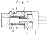
- FIG. 7 A conventional general structure of a photosemiconductor module used, for example, in optical communication is shown in Fig. 7.
- reference numeral 1 indicates a main body
- reference numeral 2 indicates a sleeve
- reference numeral 3 indicates a photosemiconductor device housing.
- the sleeve 2 has one end inserted into a sleeve supporter 4 and fixed therein and the sleeve supporter 4 is fixed to the main body 1 by welding or the like.
- the sleeve 2 is positioned at the center of an insertion hole 5 with the sleeve 2 out of contact with the inner wall of the insertion hole 5.
- the photosemiconductor device housing 3 is attached securely on the sleeve supporter side of the thus constituted receptacle 6 and an optical connector (not shown) is attached securely on the sleeve side by inserting it into the sleeve 2.
- the sleeve supporter 4 In the conventional receptacle, to attach securely the sleeve supporter 4 in which the sleeve 2 is securely inserted to the main body 1, the sleeve supporter 4 is welded to the main body, or an attaching hole is drilled in the main body and the sleeve supporter 4 is pressed into the attaching hole.
- welding since it is difficult to weld the sleeve supporter to the main body so that the sleeve may be positioned at the center precisely, there is a risk that displacement will occur highly, the assembling work is quite cumbersome, and the manufacturing cost is high. There also arises a problem of corrosion at the welded site by oxidation, leading to a defect that the durability is poor.
- the sleeve 2 In the case of securing the sleeve supporter by pressing, the sleeve 2 is fixed in the insertion hole 5 of the main body with the sleeve 2 slightly inclined depending on the degree of the exerted force due to the fitting tolerance, and similarly there is a fear that displacement will occur.
- a problem of displacement occurs, and as a result when a connector is inserted, a properly inserted state cannot be obtained, and there is a fear that every time the connector is inserted a change in the optical coupling occurs.
- the inclined arrangement of the sleeve also there is a fear that the adjustment of the optical axis at the time of the assembling is hindered.
- the main body 1 and the sleeve supporter 4 are made of metal materials, a troublesome operation that the metal materials are cut and machined to produce the main body 1 and the sleeve supporter 4 is needed, and also an assembling operation for assembling them is needed, leading to economically disadvantageous defects that the production cost is high and the receptacle is not suitable for mass production.
- An object of the present invention is to provide a receptacle wherein a sleeve can be positioned precisely in a main body so that an insertion hole for insertion of an optical connector provided in the main body and an optical connector insertion hole in the sleeve may form a single straight path whereby the insertion hole in the main body and the optical connector insertion hole in the sleeve can be arranged at all times on the same optical axis.
- Another object of the present invention is to provide a receptacle which can be easily produced and is suitable for mass production.
- the present photosemiconductor device mounting receptacle comprises a sleeve having an optical connector insertion hole, and a sleeve supporter for supporting securely said sleeve, wherein a main body of a synthetic resin is formed integrally around the sleeve by molding and is provided with an insertion hole in communication with the optical connector insertion hole of the sleeve.
- the sleeve can be placed in a proper position in the main body and as a result the insertion hole of the main body and the optical connector insertion hole of the sleeve can be arranged on the same optical axis precisely.
- the receptacle comprises a main body, a sleeve, and a sleeve supporter, and the sleeve is positioned in the main body with the the sleeve supported securely by the sleeve supporter.
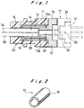
- FIG. 1 an embodiment of the present receptacle is shown, reference numerals 11, 12, and 13 indicate the main body, the sleeve, and the sleeve supporter respectively.
- the sleeve 12 is in the shape of a cylinder and has an optical connector insertion hole 14, and by fitting one end of the sleeve 12 on a projection 13a of the sleeve supporter 13 with that end aligned with the axis of the sleeve supporter 13, the sleeve 12 is supported securely by the sleeve supporter 13.
- the sleeve 12 and the sleeve supporter 13 are made of a metal such as a stainless steel and Permalloy.
- the main body 11 of a synthetic resin is formed around the sleeve 12 by molding.
- the main body 11 is connected integrally with the sleeve supporter 13 supporting securely the sleeve 12 and covers the circumference of the sleeve 12.
- the resin constituting the main body 11 As an example of the resin constituting the main body 11, a polycarbonate can be mentioned.
- the main body 11 is provided with an insertion hole 15 in communication with the optical connector insertion hole 14 of the sleeve.
- Reference numeral 16 indicates a shielding member which is formed for preventing the injected resin at the time of the molding from flowing into the sleeve and the shielding member 16 covers the circumference of the sleeve 12 with a gap between the shielding member 16 and the sleeve 12.
- the material of the shielding member 16 any material such as a metal material, for example, a stainless steel as well as a ceramic and a synthetic resin can be used.
- the sleeve supporter 13 is provided with a connecting section 18 between the main body 11 and the housing 17.
- the sleeve 12 may be a slotted sleeve produced by forming a slot 19 in a cylinder to extend axially thereof or may be a common cylindrical sleeve having no slot.
- the slotted sleeve has a diameter slightly smaller than the outer diameter of the plug of the optical connector described later.
- the present receptacle 10 constituted as stated above is produced by a generally known molding method.
- Figs. 3 and 4 illustrate one embodiment of its manufacturing method and first as is illustrated in Fig. 3, the sleeve supporter 13 on which one end of the sleeve 12 is put and secured is arranged in a molding tool 21.
- an optical path formation hole 23 of the sleeve supporter 13 is put on a protuberance 22 positioned at the axis of the molding tool so that the optical path formation hole 23 may be positioned securely.
- the generally cylindrical shielding member 16 is attached to cover the whole of the circumference of the sleeve 12.
- One end of the shielding member 16 is an open end and the other end is formed into a shielding wall 24 which is formed with an opening section 25.
- the base end section of a columnar pin 26 having a prescribed length is fixed to the molding tool 21 with the length of the the columnar pin 26 being extended in the same direction as that of the sleeve 12, the pin 26 is inserted into the opening section 25 of the shielding member 16, and the open end of the shielding member 16 is fitted on the stepped section 13b of the sleeve supporter 13. In this way, the shielding member 16 is supported by the pin 26 and the sleeve supporter 13 to be secured in position.
- the pin 26 is also inserted through the opening section 25 of the shielding member 16 into the optical connector insertion hole 14 of the sleeve 12. Therefore, the sleeve 12 and the sleeve supporter 13 are also supported securely in the molding tool by the pin 26.
- the molding tool 21 is designed in such a manner that the axis of the molding tool 21, the axis of the protuberance 22, and the axis of the pin 26 are in line.
- a melted resin is injected from an injection port 27 and is molded into the main body 11 with a prescribed shape as shown in Fig. 4.
- the injection port may be situated in a suitable position by taking the flow of the resin at the time of the molding into consideration.
- the resin injected into the molding tool flows into the resin path defining the main body 11, since the circumference of the sleeve 12 is covered with the shielding member 16 and the opening section 25 of the shielding member 16 is closed by the pin 26, the resin is prevented from flowing into the sleeve 12.
- the main body 11 molded out of the injected resin is joined integrally to the shielding member 16 and the sleeve supporter 13 and thus a molded item having the main body 11 and the sleeve component body joined together is formed.
- the photosemiconductor device housing 17 is connected to one end of the thus produced present receptacle and a plug 29 of an optical connector 28 is inserted into the other end, so that a photosemiconductor device module is formed.
- the photosemiconductor device housing 17 comprises a photosemiconductor device package 31 wherein a photosemiconductor 30 is sealed off and a lens support frame 33 to which a lens 32 is mounted, and to attach the housing 17 to the present receptacle, after the optical axes, the x axis, y axis, and z axis, are adjusted between the housing 17 and the optical fiber, the housing 17 is joined securely to the present receptacle, for example, by means of laser welding.
- the plug 29 of the optical connector 28 comprises an optical fiber 34 inserted into and integrally bonded to a fine hole at the center of the plug and the end surface of the plug 29 is finished by abrasion to have an optical surface.
- the plug 29 is inserted through the insertion hole 15 of the main body 11 into the optical connector insertion hole 14 of the sleeve 12.
- the photosemiconductor 30 may be a semiconductor light emitting device such as LD (laser diode) and LED (light emitting diode) or a semiconductor light receptive device such as PD (photodiode).
- a protuberance may be formed on the inner wall of the molding tool to act as that pin 26.
- the insertion hole 15 of the main body 11 may have diameters which are increased from the inside toward the outside as is shown in Fig. 5. Accordingly, in such a structure, the insertion hole 15 has an inclined surface 35.
- the molding tool 21 includes a pin 27 comprising a constant-diameter section 36a and a differentiated-diameter section 36b is used.
- the constant-diameter section 36a of said pin is inserted into the optical connector insertion hole 14 of the sleeve and closes the opening section 25 of the shielding member 16.
- the differentiated-diameter section 36b is positioned outside of the forward end of the shielding member 16. Then, a resin is injected to carry out the molding.
- the design is made in such a manner that the axis of the molding tool 21, the axis of the protuberance 22, and the axis of the pin 37 are in line.
- the main body is formed by molding a synthetic resin
- the production of the receptacle excludes need of the operation of welding or pressing the sleeve supporter to the main body as in the prior art, so that the defect that the secured position of the sleeve is inclined or is displaced whereby causing an error of the assembling can be obviated and the sleeve can be placed all the time on the same optical axis.
- the sleeve can be arranged on the same optical axis at all times, the adjustment of the optical axis at the time of assembling can be carried out easily.
- the main body is formed by molding, the production is easy and is suitable for mass production, and therefore there is an effect that the cost can be reduced.
- the plug of the optical connector can be mounted or dismounted smoothly, and therefore occurrence of scars due to friction at the time of mounting or dismounting can be prevented.
Abstract
Description
- The present invention relates to a photosemiconductor device mounting receptacle for coupling optically a photosemiconductor device to an optical fiber.
- A conventional general structure of a photosemiconductor module used, for example, in optical communication is shown in Fig. 7. In Fig. 7,
reference numeral 1 indicates a main body,reference numeral 2 indicates a sleeve, andreference numeral 3 indicates a photosemiconductor device housing. Thesleeve 2 has one end inserted into asleeve supporter 4 and fixed therein and thesleeve supporter 4 is fixed to themain body 1 by welding or the like. Thesleeve 2 is positioned at the center of aninsertion hole 5 with thesleeve 2 out of contact with the inner wall of theinsertion hole 5. Thephotosemiconductor device housing 3 is attached securely on the sleeve supporter side of the thus constitutedreceptacle 6 and an optical connector (not shown) is attached securely on the sleeve side by inserting it into thesleeve 2. - In the conventional receptacle, to attach securely the
sleeve supporter 4 in which thesleeve 2 is securely inserted to themain body 1, thesleeve supporter 4 is welded to the main body, or an attaching hole is drilled in the main body and thesleeve supporter 4 is pressed into the attaching hole. In the case of welding, since it is difficult to weld the sleeve supporter to the main body so that the sleeve may be positioned at the center precisely, there is a risk that displacement will occur highly, the assembling work is quite cumbersome, and the manufacturing cost is high. There also arises a problem of corrosion at the welded site by oxidation, leading to a defect that the durability is poor. - In the case of securing the sleeve supporter by pressing, the
sleeve 2 is fixed in theinsertion hole 5 of the main body with thesleeve 2 slightly inclined depending on the degree of the exerted force due to the fitting tolerance, and similarly there is a fear that displacement will occur. Thus, conventionally, to fix the sleeve supporter to the main body, a problem of displacement occurs, and as a result when a connector is inserted, a properly inserted state cannot be obtained, and there is a fear that every time the connector is inserted a change in the optical coupling occurs. Further, as a result of the inclined arrangement of the sleeve, also there is a fear that the adjustment of the optical axis at the time of the assembling is hindered. - Further, in the conventional receptacle, since the
main body 1 and thesleeve supporter 4 are made of metal materials, a troublesome operation that the metal materials are cut and machined to produce themain body 1 and thesleeve supporter 4 is needed, and also an assembling operation for assembling them is needed, leading to economically disadvantageous defects that the production cost is high and the receptacle is not suitable for mass production. -
- An object of the present invention is to provide a receptacle wherein a sleeve can be positioned precisely in a main body so that an insertion hole for insertion of an optical connector provided in the main body and an optical connector insertion hole in the sleeve may form a single straight path whereby the insertion hole in the main body and the optical connector insertion hole in the sleeve can be arranged at all times on the same optical axis.
- Another object of the present invention is to provide a receptacle which can be easily produced and is suitable for mass production.
- The present photosemiconductor device mounting receptacle comprises a sleeve having an optical connector insertion hole, and a sleeve supporter for supporting securely said sleeve, wherein a main body of a synthetic resin is formed integrally around the sleeve by molding and is provided with an insertion hole in communication with the optical connector insertion hole of the sleeve.
- When the sleeve supporter by which the sleeve is securely supported is set in a molding tool and a resin is injected into the molding tool and is molded, an integrally molded item made up of the main body and the sleeve supporter can be obtained.
- By this molding, the sleeve can be placed in a proper position in the main body and as a result the insertion hole of the main body and the optical connector insertion hole of the sleeve can be arranged on the same optical axis precisely.
-
- The objects and effects of the present invention will become apparent from the following detailed description with reference to the accompanying drawings, wherein:
- Fig. 1 is a longitudinal sectional view showing one embodiment of the present receptacle;
- Fig. 2 is a perspective view showing one embodiment of the slotted sleeve used in the present invention;
- Figs. 3 and 4 are longitudinal sectional views illustrating a method of producing the present receptacle, Fig. 3 shows the state before a resin is injected, and Fig. 4 shows the state after the resin is injected;
- Fig. 5 is a longitudinal sectional view showing another embodiment of the present receptacle;
- Fig. 6 is a longitudinal sectional view illustrating a method of producing that receptacle shown in Fig. 5; and
- Fig. 7 is a longitudinal sectional view illustrating a conventional receptacle.
- The receptacle comprises a main body, a sleeve, and a sleeve supporter, and the sleeve is positioned in the main body with the the sleeve supported securely by the sleeve supporter.
- In Fig. 1, an embodiment of the present receptacle is shown,
reference numerals sleeve 12 is in the shape of a cylinder and has an opticalconnector insertion hole 14, and by fitting one end of thesleeve 12 on aprojection 13a of thesleeve supporter 13 with that end aligned with the axis of thesleeve supporter 13, thesleeve 12 is supported securely by thesleeve supporter 13. Thesleeve 12 and thesleeve supporter 13 are made of a metal such as a stainless steel and Permalloy. Themain body 11 of a synthetic resin is formed around thesleeve 12 by molding. When themain body 11 is molded, themain body 11 is connected integrally with thesleeve supporter 13 supporting securely thesleeve 12 and covers the circumference of thesleeve 12. - As an example of the resin constituting the
main body 11, a polycarbonate can be mentioned. Themain body 11 is provided with aninsertion hole 15 in communication with the opticalconnector insertion hole 14 of the sleeve.Reference numeral 16 indicates a shielding member which is formed for preventing the injected resin at the time of the molding from flowing into the sleeve and theshielding member 16 covers the circumference of thesleeve 12 with a gap between theshielding member 16 and thesleeve 12. As the material of theshielding member 16, any material such as a metal material, for example, a stainless steel as well as a ceramic and a synthetic resin can be used. In order to allow aphotosemiconductor device housing 17 which will be described later to be welded, thesleeve supporter 13 is provided with a connectingsection 18 between themain body 11 and thehousing 17. - As is shown in Fig. 2, the
sleeve 12 may be a slotted sleeve produced by forming aslot 19 in a cylinder to extend axially thereof or may be a common cylindrical sleeve having no slot. In the case of a slotted sleeve, the slotted sleeve has a diameter slightly smaller than the outer diameter of the plug of the optical connector described later. - The present receptacle 10 constituted as stated above is produced by a generally known molding method. Figs. 3 and 4 illustrate one embodiment of its manufacturing method and first as is illustrated in Fig. 3, the
sleeve supporter 13 on which one end of thesleeve 12 is put and secured is arranged in amolding tool 21. In this arrangement, an opticalpath formation hole 23 of thesleeve supporter 13 is put on aprotuberance 22 positioned at the axis of the molding tool so that the opticalpath formation hole 23 may be positioned securely. - Then, the generally
cylindrical shielding member 16 is attached to cover the whole of the circumference of thesleeve 12. One end of theshielding member 16 is an open end and the other end is formed into ashielding wall 24 which is formed with anopening section 25. On the other hand, the base end section of acolumnar pin 26 having a prescribed length is fixed to themolding tool 21 with the length of the thecolumnar pin 26 being extended in the same direction as that of thesleeve 12, thepin 26 is inserted into theopening section 25 of theshielding member 16, and the open end of theshielding member 16 is fitted on thestepped section 13b of thesleeve supporter 13. In this way, theshielding member 16 is supported by thepin 26 and thesleeve supporter 13 to be secured in position. - Further, the
pin 26 is also inserted through theopening section 25 of theshielding member 16 into the opticalconnector insertion hole 14 of thesleeve 12. Therefore, thesleeve 12 and thesleeve supporter 13 are also supported securely in the molding tool by thepin 26. Themolding tool 21 is designed in such a manner that the axis of themolding tool 21, the axis of theprotuberance 22, and the axis of thepin 26 are in line. - As described above, after the sleeve supported by the
sleeve supporter 13 is arranged in themolding tool 21, a melted resin is injected from aninjection port 27 and is molded into themain body 11 with a prescribed shape as shown in Fig. 4. The injection port may be situated in a suitable position by taking the flow of the resin at the time of the molding into consideration. Although the resin injected into the molding tool flows into the resin path defining themain body 11, since the circumference of thesleeve 12 is covered with theshielding member 16 and theopening section 25 of theshielding member 16 is closed by thepin 26, the resin is prevented from flowing into thesleeve 12. Themain body 11 molded out of the injected resin is joined integrally to theshielding member 16 and thesleeve supporter 13 and thus a molded item having themain body 11 and the sleeve component body joined together is formed. - The
photosemiconductor device housing 17 is connected to one end of the thus produced present receptacle and aplug 29 of anoptical connector 28 is inserted into the other end, so that a photosemiconductor device module is formed. Thephotosemiconductor device housing 17 comprises aphotosemiconductor device package 31 wherein aphotosemiconductor 30 is sealed off and a lens support frame 33 to which a lens 32 is mounted, and to attach thehousing 17 to the present receptacle, after the optical axes, the x axis, y axis, and z axis, are adjusted between thehousing 17 and the optical fiber, thehousing 17 is joined securely to the present receptacle, for example, by means of laser welding. - The
plug 29 of theoptical connector 28 comprises anoptical fiber 34 inserted into and integrally bonded to a fine hole at the center of the plug and the end surface of theplug 29 is finished by abrasion to have an optical surface. Theplug 29 is inserted through theinsertion hole 15 of themain body 11 into the opticalconnector insertion hole 14 of thesleeve 12. Thephotosemiconductor 30 may be a semiconductor light emitting device such as LD (laser diode) and LED (light emitting diode) or a semiconductor light receptive device such as PD (photodiode). - In the molding tool used in producing the present receptacle, instead of the pin 26 a protuberance may be formed on the inner wall of the molding tool to act as that
pin 26. - As another embodiment of the present receptacle, the
insertion hole 15 of themain body 11 may have diameters which are increased from the inside toward the outside as is shown in Fig. 5. Accordingly, in such a structure, theinsertion hole 15 has aninclined surface 35. - To produce such a structure, as is shown in Fig. 6, the
molding tool 21 includes apin 27 comprising a constant-diameter section 36a and a differentiated-diameter section 36b is used. The constant-diameter section 36a of said pin is inserted into the opticalconnector insertion hole 14 of the sleeve and closes theopening section 25 of the shieldingmember 16. The differentiated-diameter section 36b is positioned outside of the forward end of the shieldingmember 16. Then, a resin is injected to carry out the molding. In this molding tool in this embodiment, the design is made in such a manner that the axis of themolding tool 21, the axis of theprotuberance 22, and the axis of thepin 37 are in line. - Since, in the present receptacle, the main body is formed by molding a synthetic resin, the production of the receptacle excludes need of the operation of welding or pressing the sleeve supporter to the main body as in the prior art, so that the defect that the secured position of the sleeve is inclined or is displaced whereby causing an error of the assembling can be obviated and the sleeve can be placed all the time on the same optical axis.
- As a result, when an optical connector is joined, a properly inserted state can be obtained, and there is no fear that a change in the optical coupling occurs every time the optical connector is inserted.
- Further, since the sleeve can be arranged on the same optical axis at all times, the adjustment of the optical axis at the time of assembling can be carried out easily.
- Since in the present receptacle the main body is formed by molding, the production is easy and is suitable for mass production, and therefore there is an effect that the cost can be reduced.
- Further, if the diameter of the insertion hole of the main body is increased from the inside toward the outside, the plug of the optical connector can be mounted or dismounted smoothly, and therefore occurrence of scars due to friction at the time of mounting or dismounting can be prevented.
Claims (5)
- A photosemiconductor device mounting receptacle, comprising a sleeve (12) having an optical connector insertion hole (14), and a sleeve supporter (13) for supporting securely said sleeve (12), wherein a main body (11) of a synthetic resin is formed around the sleeve (12) by molding and is provided with an insertion hole (15) in communication with the optical connector insertion hole (14) of the sleeve (12).
- A photosemiconductor device mounting receptacle as claimed in claim 1, wherein the sleeve (12) is formed into the shape of a cylinder and one end of said sleeve (12) is fitted on a projection (13a) formed on said sleeve supporter (13) to be supported securely by said sleeve supporter (13).
- A photosemiconductor device mounting receptacle as claimed in claim 1, wherein a generally cylindrical shielding member (16) that covers the circumference of the sleeve 12 and whose one end is fitted on a stepped section (13b) of the sleeve supporter (13) is provided.
- A photosemiconductor device mounting receptacle as claimed in claim 3, wherein the main body (11) is integrally connected to the shielding member (16) and the sleeve supporter (13).
- A photosemiconductor device mounting receptacle as claimed in claim 1, wherein the diameter of the insertion hole (15) of the main body (11) is increased successively from the inside toward the outside.
Applications Claiming Priority (3)
| Application Number | Priority Date | Filing Date | Title |
|---|---|---|---|
| JP336295/91 | 1991-11-26 | ||
| JP3336295A JP2552213B2 (en) | 1991-11-26 | 1991-11-26 | Optical semiconductor element mounting receptacle |
| US07/995,019 US5307435A (en) | 1991-11-26 | 1992-12-22 | Photosemiconductor device mounting receptacle |
Publications (2)
| Publication Number | Publication Date |
|---|---|
| EP0544149A1 true EP0544149A1 (en) | 1993-06-02 |
| EP0544149B1 EP0544149B1 (en) | 1996-04-17 |
Family
ID=26575422
Family Applications (1)
| Application Number | Title | Priority Date | Filing Date |
|---|---|---|---|
| EP92119321A Expired - Lifetime EP0544149B1 (en) | 1991-11-26 | 1992-11-12 | Photosemiconductor device mounting receptacle |
Country Status (3)
| Country | Link |
|---|---|
| US (1) | US5307435A (en) |
| EP (1) | EP0544149B1 (en) |
| JP (1) | JP2552213B2 (en) |
Cited By (6)
| Publication number | Priority date | Publication date | Assignee | Title |
|---|---|---|---|---|
| GB2283832A (en) * | 1993-11-09 | 1995-05-17 | Sanyo Electric Co | Coupling optic fibre to a light source using reflecting means |
| GB2303964A (en) * | 1995-05-29 | 1997-03-05 | Oki Electric Ind Co Ltd | Photoelectric sensor light guide |
| EP0690324A3 (en) * | 1994-06-30 | 1997-03-26 | Hamamatsu Photonics Kk | Receptacle for optical fiber connection and method of manufacturing the same |
| GB2271682B (en) * | 1992-10-13 | 1997-03-26 | Marconi Gec Ltd | Improvements in or relating to connectors |
| EP1063548A1 (en) * | 1999-06-25 | 2000-12-27 | Lucent Technologies Inc. | Plastic packaged optoelectronic device |
| CN103270444A (en) * | 2010-12-24 | 2013-08-28 | 株式会社自动网络技术研究所 | Optical assembly |
Families Citing this family (19)
| Publication number | Priority date | Publication date | Assignee | Title |
|---|---|---|---|---|
| DE4114156A1 (en) * | 1991-04-30 | 1992-11-05 | Burndy Deutschland | CONNECTOR FOR LIGHTWAVE GUIDE |
| DE4300652C1 (en) * | 1993-01-13 | 1994-03-31 | Bosch Gmbh Robert | Hybrid integrated optical circuit manufacturing method - uses shaping tool into which electro-optical semiconductor component is inserted before enclosing in polymer material |
| JP3087561B2 (en) * | 1993-12-28 | 2000-09-11 | 三菱電機株式会社 | Optical semiconductor module and manufacturing method thereof |
| JP3518695B2 (en) * | 1994-04-28 | 2004-04-12 | アルプス電気株式会社 | Optical fiber connector |
| CA2161718A1 (en) * | 1994-10-31 | 1996-05-01 | Hiromi Kurashima | Optical module having structure for defining fixing position of sleeve |
| JPH09218324A (en) * | 1996-02-08 | 1997-08-19 | Alps Electric Co Ltd | Light emission module |
| JP3657711B2 (en) * | 1996-10-14 | 2005-06-08 | 三菱電機株式会社 | Light emitting element module and light emitting element module holder |
| US6012267A (en) * | 1998-02-26 | 2000-01-11 | Tetra Laval Holdings & Finance, Sa | Hygienic packaging machine |
| JP3654051B2 (en) * | 1999-06-01 | 2005-06-02 | モレックス インコーポレーテッド | Receptacle type optical connector |
| US6517258B1 (en) * | 1999-06-25 | 2003-02-11 | Agere Systems Inc. | Plastic packaged optoelectronic device |
| JP2001242356A (en) * | 2000-02-28 | 2001-09-07 | Alps Electric Co Ltd | Optical fiber connector and optical communication module using it |
| JP2003098407A (en) * | 2001-09-26 | 2003-04-03 | Nec Compound Semiconductor Devices Ltd | Semiconductor optical coupling device |
| JP2005292339A (en) * | 2004-03-31 | 2005-10-20 | Sumitomo Electric Ind Ltd | Optical module |
| JP4706856B2 (en) * | 2006-04-18 | 2011-06-22 | 住友電気工業株式会社 | Optical receptacle |
| US7993064B2 (en) * | 2008-04-01 | 2011-08-09 | General Electric Company | Photonic power devices and methods of manufacturing the same |
| JP5262538B2 (en) * | 2008-10-03 | 2013-08-14 | 日亜化学工業株式会社 | Optical receptacle and optical module using the same |
| JP5625893B2 (en) * | 2010-12-24 | 2014-11-19 | 株式会社オートネットワーク技術研究所 | Optical connector |
| WO2012141065A1 (en) * | 2011-04-12 | 2012-10-18 | 株式会社オートネットワーク技術研究所 | Optical module and optical module manufacturing method |
| US10502902B2 (en) | 2015-09-30 | 2019-12-10 | Sony Corporation | Optical communication connector, optical communication cable, and electronic device |
Citations (3)
| Publication number | Priority date | Publication date | Assignee | Title |
|---|---|---|---|---|
| US4173389A (en) * | 1977-09-28 | 1979-11-06 | Bell Telephone Laboratories, Incorporated | Molded optical fiber connector |
| US4281891A (en) * | 1978-03-27 | 1981-08-04 | Nippon Electric Co., Ltd. | Device for excellently coupling a laser beam to a transmission medium through a lens |
| EP0053482A2 (en) * | 1980-11-28 | 1982-06-09 | Kabushiki Kaisha Toshiba | Module for a fiber optic link |
Family Cites Families (15)
| Publication number | Priority date | Publication date | Assignee | Title |
|---|---|---|---|---|
| US4186996A (en) * | 1978-09-22 | 1980-02-05 | Amp Incorporated | Optic adaptor junction |
| JPS5674212A (en) * | 1979-11-22 | 1981-06-19 | Fujitsu Ltd | Connection method for optical fiber |
| US4737011A (en) * | 1984-07-13 | 1988-04-12 | Dainichi-Nippon Cables Ltd. | Connector for high energy beam |
| AU572342B2 (en) * | 1984-09-04 | 1988-05-05 | Nippon Telegraph & Telephone Corporation | Optical connector |
| JPS6259908A (en) * | 1985-09-10 | 1987-03-16 | Matsuo Sangyo Kk | Formation of terminal fixing means for optical fiber |
| US4803361A (en) * | 1986-05-26 | 1989-02-07 | Hitachi, Ltd. | Photoelectric device with optical fiber and laser emitting chip |
| US4834494A (en) * | 1987-07-20 | 1989-05-30 | Corning Glass Works | Expanded beam waveguide connector |
| JPH02124504A (en) * | 1988-11-02 | 1990-05-11 | Toshiba Corp | Photodetecting module |
| JP2684219B2 (en) * | 1989-07-05 | 1997-12-03 | 三菱電機株式会社 | Optical semiconductor module |
| JPH0326487U (en) * | 1989-07-20 | 1991-03-18 | ||
| JPH03153203A (en) * | 1989-11-10 | 1991-07-01 | Matsushita Electric Ind Co Ltd | Optical connector |
| US5119462A (en) * | 1990-01-29 | 1992-06-02 | 501 Nippon Sheet Glass Co., Ltd. | Photosemiconductor and optical fiber welded module |
| US5189716A (en) * | 1990-01-29 | 1993-02-23 | Nippon Sheet Glass Co., Ltd. | Photosemiconductor and optical fiber welded module |
| JP2570879B2 (en) * | 1990-02-08 | 1997-01-16 | 三菱電機株式会社 | Assembly method of optical semiconductor module |
| US5121455A (en) * | 1990-09-11 | 1992-06-09 | Methode Electronics, Inc. | Fiber optic connector |
-
1991
- 1991-11-26 JP JP3336295A patent/JP2552213B2/en not_active Expired - Fee Related
-
1992
- 1992-11-12 EP EP92119321A patent/EP0544149B1/en not_active Expired - Lifetime
- 1992-12-22 US US07/995,019 patent/US5307435A/en not_active Expired - Lifetime
Patent Citations (3)
| Publication number | Priority date | Publication date | Assignee | Title |
|---|---|---|---|---|
| US4173389A (en) * | 1977-09-28 | 1979-11-06 | Bell Telephone Laboratories, Incorporated | Molded optical fiber connector |
| US4281891A (en) * | 1978-03-27 | 1981-08-04 | Nippon Electric Co., Ltd. | Device for excellently coupling a laser beam to a transmission medium through a lens |
| EP0053482A2 (en) * | 1980-11-28 | 1982-06-09 | Kabushiki Kaisha Toshiba | Module for a fiber optic link |
Non-Patent Citations (2)
| Title |
|---|
| PATENT ABSTRACTS OF JAPAN vol. 10, no. 271 (P-497)16 September 1986 & JP-A-61 094 010 ( FURUKAWA ELCTRIC CO LTD ) 12 May 1986 * |
| PATENT ABSTRACTS OF JAPAN vol. 13, no. 5000 (P-979)20 December 1989 & JP-A-01 243 007 ( NEC CORP ) 27 September 1989 * |
Cited By (13)
| Publication number | Priority date | Publication date | Assignee | Title |
|---|---|---|---|---|
| GB2271682B (en) * | 1992-10-13 | 1997-03-26 | Marconi Gec Ltd | Improvements in or relating to connectors |
| US5727103A (en) * | 1993-11-09 | 1998-03-10 | Sanyo Electric Co., Ltd. | Optical leakage preventing apparatus and self-light-emitting indicating apparatus using the same |
| GB2283832B (en) * | 1993-11-09 | 1998-01-21 | Sanyo Electric Co | Improvements relating to sign illumination |
| GB2283832A (en) * | 1993-11-09 | 1995-05-17 | Sanyo Electric Co | Coupling optic fibre to a light source using reflecting means |
| EP0690324A3 (en) * | 1994-06-30 | 1997-03-26 | Hamamatsu Photonics Kk | Receptacle for optical fiber connection and method of manufacturing the same |
| US5684903A (en) * | 1994-06-30 | 1997-11-04 | Hamamatsu Photonics K.K. | Receptacle and method of manufacturing the same |
| GB2303964A (en) * | 1995-05-29 | 1997-03-05 | Oki Electric Ind Co Ltd | Photoelectric sensor light guide |
| US5767508A (en) * | 1995-05-29 | 1998-06-16 | Oki Electric Industry Co., Ltd. | Photoelectric sensor having a light guide built-in |
| GB2303964B (en) * | 1995-05-29 | 2000-06-07 | Oki Electric Ind Co Ltd | Photoelectric sensor having a light guide built-in |
| EP1063548A1 (en) * | 1999-06-25 | 2000-12-27 | Lucent Technologies Inc. | Plastic packaged optoelectronic device |
| US6371665B1 (en) | 1999-06-25 | 2002-04-16 | Lucent Technologies Inc. | Plastic packaged optoelectronic device |
| CN103270444A (en) * | 2010-12-24 | 2013-08-28 | 株式会社自动网络技术研究所 | Optical assembly |
| CN103270444B (en) * | 2010-12-24 | 2015-02-18 | 株式会社自动网络技术研究所 | Optical assembly |
Also Published As
| Publication number | Publication date |
|---|---|
| US5307435A (en) | 1994-04-26 |
| JP2552213B2 (en) | 1996-11-06 |
| JPH05150144A (en) | 1993-06-18 |
| EP0544149B1 (en) | 1996-04-17 |
Similar Documents
| Publication | Publication Date | Title |
|---|---|---|
| US5307435A (en) | Photosemiconductor device mounting receptacle | |
| US5526455A (en) | Connector including opposing lens surfaces, side surfaces, and contact surfaces for coupling optical devices | |
| US5537503A (en) | Optical semiconductor module and method of fabricating the same | |
| US4988159A (en) | Fiber tailed optoelectronic transducer | |
| US6749347B1 (en) | Laser diode module and assembling method therefor | |
| US5333224A (en) | Photoelectric converter connecting device | |
| US5973862A (en) | Optical module | |
| US6270263B1 (en) | Optical module | |
| US4383731A (en) | Opto-electronic head incorporating a very small diameter optical fibre portion and connection device incorporating such a head | |
| US4302070A (en) | Optoelectronic semiconductor device having an optical fiber connector | |
| US20050244109A1 (en) | Optical sub-assembly having an enhanced discharge-resistant arrangement and an optical transceiver using the same | |
| CA2172749C (en) | Device for optical connection of an optical element, for example an optical fibre, with a lens | |
| US5119462A (en) | Photosemiconductor and optical fiber welded module | |
| US5687270A (en) | Photodetector module capable of preventing deviation of optical axis | |
| US5189716A (en) | Photosemiconductor and optical fiber welded module | |
| US5631990A (en) | Integrated optical module for coupling an optical fiber to an optical device | |
| US6547455B1 (en) | Optical module for a semiconductor light-emitting device | |
| US20040218857A1 (en) | Duplex optical transceiver module | |
| US20040141697A1 (en) | Optoelectronic transmitter module and method for the production thereof | |
| JPH07134225A (en) | Sleeve-integrated lens and optical coupling element module formed by using this lens | |
| US6059463A (en) | Electro-optical device | |
| JPH0961673A (en) | Optical semiconductor module | |
| US11415746B2 (en) | Sensor | |
| US6425696B1 (en) | Molded fiber optic ferrule receptable | |
| JPH03259106A (en) | Coupler for receptacle type photosemiconductor |
Legal Events
| Date | Code | Title | Description |
|---|---|---|---|
| PUAI | Public reference made under article 153(3) epc to a published international application that has entered the european phase |
Free format text: ORIGINAL CODE: 0009012 |
|
| AK | Designated contracting states |
Kind code of ref document: A1 Designated state(s): CH DE FR GB IT LI NL |
|
| 17P | Request for examination filed |
Effective date: 19930728 |
|
| 17Q | First examination report despatched |
Effective date: 19940922 |
|
| GRAH | Despatch of communication of intention to grant a patent |
Free format text: ORIGINAL CODE: EPIDOS IGRA |
|
| GRAA | (expected) grant |
Free format text: ORIGINAL CODE: 0009210 |
|
| AK | Designated contracting states |
Kind code of ref document: B1 Designated state(s): CH DE FR GB IT LI NL |
|
| REF | Corresponds to: |
Ref document number: 69209980 Country of ref document: DE Date of ref document: 19960523 |
|
| ITF | It: translation for a ep patent filed |
Owner name: BARZANO' E ZANARDO ROMA S.P.A. |
|
| ET | Fr: translation filed | ||
| REG | Reference to a national code |
Ref country code: CH Ref legal event code: NV Representative=s name: TROESCH SCHEIDEGGER WERNER AG |
|
| PLBE | No opposition filed within time limit |
Free format text: ORIGINAL CODE: 0009261 |
|
| STAA | Information on the status of an ep patent application or granted ep patent |
Free format text: STATUS: NO OPPOSITION FILED WITHIN TIME LIMIT |
|
| 26N | No opposition filed | ||
| REG | Reference to a national code |
Ref country code: GB Ref legal event code: IF02 |
|
| PGFP | Annual fee paid to national office [announced via postgrant information from national office to epo] |
Ref country code: NL Payment date: 20061116 Year of fee payment: 15 |
|
| PGFP | Annual fee paid to national office [announced via postgrant information from national office to epo] |
Ref country code: FR Payment date: 20061117 Year of fee payment: 15 |
|
| PGFP | Annual fee paid to national office [announced via postgrant information from national office to epo] |
Ref country code: GB Payment date: 20061123 Year of fee payment: 15 Ref country code: CH Payment date: 20061123 Year of fee payment: 15 |
|
| PGFP | Annual fee paid to national office [announced via postgrant information from national office to epo] |
Ref country code: IT Payment date: 20061130 Year of fee payment: 15 |
|
| PGFP | Annual fee paid to national office [announced via postgrant information from national office to epo] |
Ref country code: DE Payment date: 20070126 Year of fee payment: 15 |
|
| GBPC | Gb: european patent ceased through non-payment of renewal fee |
Effective date: 20071112 |
|
| PG25 | Lapsed in a contracting state [announced via postgrant information from national office to epo] |
Ref country code: CH Free format text: LAPSE BECAUSE OF NON-PAYMENT OF DUE FEES Effective date: 20071130 Ref country code: LI Free format text: LAPSE BECAUSE OF NON-PAYMENT OF DUE FEES Effective date: 20071130 |
|
| REG | Reference to a national code |
Ref country code: CH Ref legal event code: PL |
|
| NLV4 | Nl: lapsed or anulled due to non-payment of the annual fee |
Effective date: 20080601 |
|
| PG25 | Lapsed in a contracting state [announced via postgrant information from national office to epo] |
Ref country code: DE Free format text: LAPSE BECAUSE OF NON-PAYMENT OF DUE FEES Effective date: 20080603 Ref country code: NL Free format text: LAPSE BECAUSE OF NON-PAYMENT OF DUE FEES Effective date: 20080601 |
|
| REG | Reference to a national code |
Ref country code: FR Ref legal event code: ST Effective date: 20080930 |
|
| PG25 | Lapsed in a contracting state [announced via postgrant information from national office to epo] |
Ref country code: GB Free format text: LAPSE BECAUSE OF NON-PAYMENT OF DUE FEES Effective date: 20071112 |
|
| PG25 | Lapsed in a contracting state [announced via postgrant information from national office to epo] |
Ref country code: FR Free format text: LAPSE BECAUSE OF NON-PAYMENT OF DUE FEES Effective date: 20071130 |
|
| PG25 | Lapsed in a contracting state [announced via postgrant information from national office to epo] |
Ref country code: IT Free format text: LAPSE BECAUSE OF NON-PAYMENT OF DUE FEES Effective date: 20071112 |