EP0550751A1 - Nonvolatile semiconductor memory - Google Patents
Nonvolatile semiconductor memory Download PDFInfo
- Publication number
- EP0550751A1 EP0550751A1 EP91916788A EP91916788A EP0550751A1 EP 0550751 A1 EP0550751 A1 EP 0550751A1 EP 91916788 A EP91916788 A EP 91916788A EP 91916788 A EP91916788 A EP 91916788A EP 0550751 A1 EP0550751 A1 EP 0550751A1
- Authority
- EP
- European Patent Office
- Prior art keywords
- source
- circuit
- cell
- block
- erase
- Prior art date
- Legal status (The legal status is an assumption and is not a legal conclusion. Google has not performed a legal analysis and makes no representation as to the accuracy of the status listed.)
- Granted
Links
- 239000004065 semiconductor Substances 0.000 title claims description 12
- 230000015654 memory Effects 0.000 claims abstract description 39
- 239000011159 matrix material Substances 0.000 claims 1
- 230000005684 electric field Effects 0.000 abstract description 14
- 230000007257 malfunction Effects 0.000 abstract description 8
- 238000010586 diagram Methods 0.000 description 20
- 238000007599 discharging Methods 0.000 description 11
- 230000010355 oscillation Effects 0.000 description 6
- 230000004075 alteration Effects 0.000 description 5
- 230000003111 delayed effect Effects 0.000 description 4
- 230000006870 function Effects 0.000 description 4
- 238000000034 method Methods 0.000 description 4
- 230000008878 coupling Effects 0.000 description 2
- 238000010168 coupling process Methods 0.000 description 2
- 238000005859 coupling reaction Methods 0.000 description 2
- 230000000694 effects Effects 0.000 description 2
- 239000002784 hot electron Substances 0.000 description 2
- 101100481702 Arabidopsis thaliana TMK1 gene Proteins 0.000 description 1
- 101150022905 RDR1 gene Proteins 0.000 description 1
- 101150066141 RDR2 gene Proteins 0.000 description 1
- 101150060692 RDR4 gene Proteins 0.000 description 1
- 230000015556 catabolic process Effects 0.000 description 1
- 230000008859 change Effects 0.000 description 1
- 230000001419 dependent effect Effects 0.000 description 1
- 230000010354 integration Effects 0.000 description 1
- 239000000463 material Substances 0.000 description 1
- 230000000630 rising effect Effects 0.000 description 1
- 230000009466 transformation Effects 0.000 description 1
Images


Classifications
-
- G—PHYSICS
- G11—INFORMATION STORAGE
- G11C—STATIC STORES
- G11C16/00—Erasable programmable read-only memories
- G11C16/02—Erasable programmable read-only memories electrically programmable
- G11C16/06—Auxiliary circuits, e.g. for writing into memory
- G11C16/10—Programming or data input circuits
- G11C16/14—Circuits for erasing electrically, e.g. erase voltage switching circuits
- G11C16/16—Circuits for erasing electrically, e.g. erase voltage switching circuits for erasing blocks, e.g. arrays, words, groups
-
- G—PHYSICS
- G11—INFORMATION STORAGE
- G11C—STATIC STORES
- G11C16/00—Erasable programmable read-only memories
- G11C16/02—Erasable programmable read-only memories electrically programmable
-
- G—PHYSICS
- G11—INFORMATION STORAGE
- G11C—STATIC STORES
- G11C16/00—Erasable programmable read-only memories
- G11C16/02—Erasable programmable read-only memories electrically programmable
- G11C16/06—Auxiliary circuits, e.g. for writing into memory
- G11C16/10—Programming or data input circuits
- G11C16/12—Programming voltage switching circuits
-
- G—PHYSICS
- G11—INFORMATION STORAGE
- G11C—STATIC STORES
- G11C16/00—Erasable programmable read-only memories
- G11C16/02—Erasable programmable read-only memories electrically programmable
- G11C16/06—Auxiliary circuits, e.g. for writing into memory
- G11C16/34—Determination of programming status, e.g. threshold voltage, overprogramming or underprogramming, retention
- G11C16/3418—Disturbance prevention or evaluation; Refreshing of disturbed memory data
Definitions
- the present invention relates to a non-volatile semiconductor memory, and more particularly to a non-volatile semiconductor memory having a plurality block of non-volatile memory cells of two-layered structure, capable of altering data in units of block.
- All-bit flash erase type memories have drawn attention as electrically erasable, programmable read-only memories (E2PROM).
- E2PROM electrically erasable, programmable read-only memories
- Recent requirements for such memories are to provide a function of altering data in each of a plurality of memory blocks in units of block. For example, a 4 M bit device is divided into 16 blocks each having 32 K bytes or into 4 blocks each having 256 K bytes, and data erasure is required to be performed on the block unit basis. With such block division of a cell array, cells in a plurality of different blocks are connected to the same word line or data line. Therefore, repeating write/erase of a particular block may apply stress to cells in other non-selected blocks.
- the characteristic structure of such a cell resides in that the gate oxide film under the floating gate is about 100 angstroms thinner than that of an EPROM cell because a tunnel current flows between the floating gate and source during data erase, and that the superposing area of the source n+ region and the floating gate is made wider than that of EPROM.
- a cell in an erase state or write state in a non-selected block is shown in Table 1.
- a cell in an erase state in a non-selected block connected to a selected word line is applied to an electric field of about 7.5 MV/cm between its floating gate and source, and a cell in a write state in a non-selected block connected to a selected data line is applied to an electric field of about 6.5 MV/cm between its floating gate and drain.
- a conventional device is associated with the problem that as data write and erase are effected to a selected block, data write error and erase error may occur at non-selected blocks.
- This scheme is characterized in that a plurality of memory cells connected to one selected word line can be erased at the same time. It is now assumed that a word line WL1 is selected and another word line WL2 is not selected in a data erase mode. Specifically, the selected word line WL1 is applied with a voltage VWL1 of -10 V, the non-selected word line WL2 is applied with a voltage VWL2 of 5 V, a source voltage VS is set to 5 V, and data lines DL1 and DL2 are set to a floating state. In this state, memory cells M1 and M2 enter an erase state, and memory cells M3 and M4 enter a non-erase state. In a program mode (in a data write mode), hot electrons are injected into a floating gate FG. In a read mode, a sense amplifier judges whether a selected cell is being turned on (a cell current flows) or off (a cell current will not flow).
- the above-described scheme has the following problems.
- WL2 is set to 5 V
- VS is set to 5 V
- DL1 and DL2 enter the floating state.
- the data lines DL1 and DL2 are charged via the non-selected cells M3 and M4 up to (5 V - V th ) where V th is a cell threshold value.
- a cell current for charging the data lines DL1 and DL2 flows in the non-selected cells M3 and M4 during the time period from t1 to t2, therefore leading to a possibility of write error at the non-selected cells M3 and M4.
- a memory cell array is divided into a plurality of blocks.
- a moderating voltage is applied to the source or control gate of a memory cell in another block (non-selected block) to moderate stress between the floating gate and source/drain, thereby preventing write error and erase error.
- the source and drain of a memory cell in the non-selected block are equalized to moderate an electric field between the control gate and source/drain and not to flow a channel current, thereby preventing write error.
- the source and data lines are equalized prior to setting the source line and word line of a cell in a non-selected block to an erase voltage.
- the equalization operation is released after the erase operation, thereby preventing malfunction of a non-selected cell.
- Fig. 1 is a diagram showing the overall arrangement of an embodiment according to the present invention.
- Fig. 2 is a circuit diagram showing the details of a portion of the embodiment shown in Fig. 1.
- Figs. 3 to 7 are circuit diagrams showing examples of the block erase circuit of the embodiment shown in Fig. 1.
- Fig. 8 is a circuit diagram showing the details of the column gate section.
- Fig. 9 is a circuit diagram showing the main portion of the row decoder.
- Fig. 10 is a graph showing the characteristics of a memory cell in a non-selected block.
- Fig. 11 is a diagram showing the overall arrangement of another embodiment according to the present invention.
- Fig. 12 is a circuit diagram showing the details of a portion of the embodiment shown in Fig. 11.
- Fig. 13 is a diagram showing the overall arrangement of another embodiment according to the present invention.
- Fig. 14 is a timing chart explaining the operation of the embodiment shown in Fig. 13.
- Fig. 15 is a circuit diagram of the program control circuit shown in Fig. 13.
- Fig. 16 is a circuit diagram showing an example of the block erase circuit shown in Fig. 13.
- Fig. 17 is a circuit diagram showing another example of the block erase circuit.
- Fig. 18 is a circuit diagram showing another example of the block erase circuit.
- Fig. 19 is a circuit diagram of a stress moderating circuit.
- Figs. 20A and 20B are diagrams explaining the relationship between cell array division and current consumption.
- Fig. 21 is a conceptual view showing another embodiment of the present invention.
- Fig. 22 is a timing chart explaining the operation of the embodiment shown in Fig. 21.
- Figs. 23A and 23B illustrate the states of a selected word line and non-selected word line shown in Fig. 21 during an erase mode.
- Figs. 24A and 24B illustrate the states of a selected word line and non-selected word line shown in Fig. 21 during the program mode.
- Fig. 25 illustrates the state of the row decoder shown in Fig. 21 during the read mode.
- Figs. 26A and 26B illustrate the state of the negative bias circuit shown in Fig. 21 during the erase mode and other modes.
- Fig. 27 is a circuit diagram of the source bias circuit shown in Fig. 21.
- Fig. 28 is a conceptual diagram showing the overall arrangement of another embodiment according to the present invention.
- Fig. 29 is a conceptual diagram of a conventional memory device.
- Fig. 30 is a timing chart explaining the operation of the conventional memory device.
- Fig. 1 shows a device whose memory cell array is divided into sixteen blocks in the data line direction according to the first embodiment.
- the memory cell array 1 is divided into sixteen blocks 2 each provided with a block erase circuit 3.
- reference numeral 5 represents a row decoder
- reference numeral 6 represents a column decoder
- reference numeral 7 represents a row pre-decoder.
- the details of each block 2 are shown in Fig. 2.
- each block erase circuit 3 is commonly connected to the sources of cells C XY in each block 2.
- Cells commonly connected to one data line DL ⁇ are located within the same block.
- Cells commonly connected to one word line WL i are located over a plurality of blocks.
- a predetermined potential moderating potential
- the electric field between the floating gate and source becomes about 5 MV/cm which moderates the electric field by about 2.5 MV/cm as compared with about 7.5 MV/cm when 0 V is applied to the cell source.
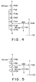
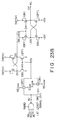
- Fig. 3 is an example of a circuit diagram of the block erase circuit 3 according to the present invention.
- This circuit is constructed of a block selecting unit 11, a level shifter 12, a charge transistor T116, discharge transistors T120 and T121, a delay circuit 13, and a non-selected block bias circuit 14.
- the block selecting circuit has a NOR gate NR100 calculating a NOR between an address selection signal BS and a signal NErase, the address selection signal BS being supplied from a NAND gate NA100 to which a block selection address BSA is inputted.
- the level shifter 12 is constructed of transistors T110 to T115 and an inverter I110.
- the charge transistor T116 is used for charging the selected block 2.
- the discharge transistors T120 and T121 are used for discharging electric charges from the cell sources during the time period except for the erase operation.
- the delay circuit 13 is used for controlling the timing of discharge, and is constructed of inverters I120 to I124, and a NAND gate NA120.
- the non-selected block bias circuit 14 is constructed of transistors T130 to T132, and resistors R130 and R131.
- the block erase circuit 3 of a block 2 selected by an address takes a state that an output BS of NA100 becomes “L”, the signal NErase becomes “L”, and an output EA of NR100 becomes “H”.
- the discharge transistors T120 and T121 turn off, the gates of which are applied with NErase and its delayed signal, respectively.
- current flows from the transistor T130 to the resistors R130 and R131 and to ground, setting a node NEG to an intermediate potential.
- the transistor T132 has a low gate voltage so that it turns off.
- the signal NErase becomes "L”
- the transistor T130 turns on
- the transistor T131 turns off, and current flows from T130 to the resistors R130 and R131 and to ground. Therefore, the node NEG between R131 and R131 takes a potential determined by the resistances of T130, R130, and R131.
- the cell sources are therefore charged through T132 and set to the potential of NEG - V TH (T132). For example, assuming that NEG is 3 V, and V TH of T132 is 1 V, then the cell sources are set to 2 V. At this time, similar to the case of the block erase circuit 3 connected to the selected block, the discharge transistors T120 and T121 turn off.
- the signal NErase becomes "H".
- the charge transistor T116 turns off, and for the non-selected block 2, the transistor T130 turns off, the transistor T131 turns on, and the charge transistor T132 turns off.
- the transistor T120 turns on to start discharging the cell sources.
- the gate of the transistor T121 becomes "H” after a predetermined time delay set by the delay circuit 13, to discharge the transistor T121.
- the reason why two transistors T120 and T121 are used for discharge is that an excessive peak current will flow if discharge is performed by a transistor of large dimension, because the junction capacity of the cell source region is large.
- the dimension of the transistor T120 is set small to gradually discharge.
- discharge is further performed by the transistor T121 whose dimension is set large.
- the reason why the dimension of the transistor T121 is set large is to prevent the cell sources SC from floating above 0 V (ground) during a read or program mode. Particularly in the program mode, a current of several mA flows so that it is necessary to set W to about several hundreds to 1000 ⁇ m.
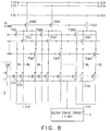
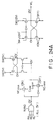
- FIGS. 4 to 7 Other examples of the non-selected block bias circuit of the block erase circuit 3 are shown in Figs. 4 to 7.
- the resistors R130 and R131 shown in Fig. 3 are replaced by transistors. Namely, the resistor R130 is replaced by transistors T141 to T144, and the resistor R131 is replaced by transistors T145 and T146. Basically, the gate potential NEG of a charge transistor T148 is determined by a division ratio of resistors.
- the gate potential NEG of a charge transistor T155 is determined by the values V TH of transistors T152 and T153.
- the node NEG is set to 2 V TH and the cell sources are set to about V TH level.
- the potential at the cell sources CS is determined by V TH of a D-type transistor T161.
- the signal NErase becomes "L”
- a transistor T160 turns on
- the gate of the transistor T161 becomes "L”.
- the cell sources in a non-selected block are charged to a value V TH of the D-type transistor T161, i.e., to about 1 to 2 V.
- the circuits shown in Figs. 6 and 7 save power because current will not flow always as in the circuits shown in Figs. 3 to 5.
- the above-described circuits turn off upon reception of NErase + "H" during the program, read, and stand-by modes except the erase mode.
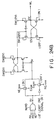
- Fig. 8 shows the structure of the column gate.
- Fig. 8 corresponding to Fig. 1 shows the column structure of one block, a row decoder buffer, a word line, and cells C111 to C 1m1 connected to the word line.
- This device is obtained, for example, by dividing a 4 M bit cell array into sixteen blocks in the data line direction at intervals of 32 K bytes.
- One block has 128 data lines for 8 I/O units each I/O assigned 16 data lines.
- One byte is selected by one of column signals h1 to h16.
- Each block is selected by one of column signals s1 to s16.
- T200 to T207 represent column gate transistors for selecting a block
- T210 to T287 represent column gate transistors selected by the column signal h1 to h16.
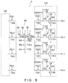
- Fig. 9 shows the structure of the row decoder 5.
- MD represents a main decoder having a plurality of transistors T350 to T355 and selected by outputs RAi, RBi, and RCi from the row pre-decoder
- T300, T310, T320, T330, T340 to T343 represent transfer gates selected by outputs RDR i and RDL i from the row pre-decoder
- T300', T310', T320', and T330' represent charge transistors
- T301 to T303, T311 to T313, T321 to T323, and T331 to T333 represent feedback-type inverters.
- a circuit CIR at the left side of Fig. 9 has the same structure as the circuit CIR at the right side.
- RDR1 for selecting the word line WL1 becomes "H”
- NRDR1 becomes "L”
- Other RDR2 to RDR4 become “L”
- other NRDR2 to NRDR4 become "H”.
- the transistor T302 turns on and the transistor T303 turns off, so the word line WL1 takes an SW potential.
- the transistors T312, T322, and T332 turn off T313, T323, and T333 turn on, so the other word lines WL2 to WL4 take a ground level.
- first to eighth blocks 2 and ninth to sixteenth blocks 2 are grouped on opposite sides of the row decoder 5 as shown in Fig. 1.
- the right transfer gate RDRi executes a logical calculation with a block selecting column signal Si to drive only the right word line connected to the selected block.
- the left transfer gate RDLi executes a logical calculation with the block selecting column signal Si to drive only the left word line connected to the selected block.
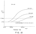
- Fig. 10 is a graph showing the relationship between time duration of stress applied to the control gate of an erased cell in a non-selected block and a change in cell V TH .
- the cell source is assumed to be set to 0 V.
- the control gate stress time period becomes long, the cell V TH rises. This rise is dependent upon the control gate potential.
- E sf electric field
- V TH0 and V THMax are herein introduced, the term V TH0 being a V TH of a cell in an erase state without no stress, and the term V THMax being a limit V TH of a cell providing no access time delay and no read error.
- the stress time period of cells in a non-selected block is about 800 sec, enabling to prevent malfunction to be caused by stress.
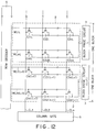
- a memory cell array is divided into blocks in the word line direction. Similar to the first embodiment, a block erase circuit 3 is provided at each block. The layout of cells is shown in Fig. 12. Cells C commonly connected to a word line WL are located within the same block. On the other hand, cells C commonly connected to a data line CL are located over a plurality of blocks. With such an arrangement, one data line CL is commonly connected to all corresponding cells in first to sixteenth blocks.
- a row decoder 5 selects a particular block 2 by applying a high potential to a word line WL of the block 2, while raising the potentials of other word lines WL in non-selected blocks to a potential, for example, a potential half that of the word line WL of the selected block.
- a circuit for raising the potential of word lines of non-selected blocks may use any general circuit for raising a word line potential.
- Stress applied to a cell in a non-selected block can be moderated even in the case of a flash-type E2PROM cell array divided into blocks for data alteration on the block unit basis. For example, even if data alteration is repeated 105 times with respect to a particular block, the V TH variation of a cell in a non-selected block can be sufficiently suppressed.
- an erase on the block unit basis is possible, providing value-added performance and an increased number of write/erase cycles with high reliability.
- the source and drain of a memory cell in a non-selected block are biased to the same potential at the same time to moderate the electric field between the control gate and source/drain and not to flow a channel current, thereby preventing write error and improving the reliability.
- Fig. 13 shows the overall structure of this embodiment.
- a cell array is divided into a plurality of blocks 2i (21, 22, ...) in the data line DL i direction.
- This memory device is provided with a stress moderating circuit SE shared by all blocks, and block erase circuits BE1, BE2, ... connected to corresponding source lines SL1, SL2, ... of respective blocks.
- the source line SL1 is connected to data lines DL11 to DL n1 via transfer gates TEQ11 to TEQ n1 to the gates of which an output signal SDI(1) from the block erase circuit BE1 is applied.
- GSE Stress moderating circuit SE
- PHC write potential raising circuit
- CG represents a column gate
- RD represents a row decoder
- EC represents an erase control circuit.
- the block 21 is selected and a cell C111 is selected to write data therein.
- the selected word line WL1 and data line DL11 are connected to the write potential raising circuit PHC via the row decoder RD and column gate CG to write data in the selected cell C n1 .
- the output signals SDI(1) and SSI(1) of the block erase circuit BE1 of the selected block 21 take a level "L", and the source line SL1 is disconnected from the data line DL11 and from the output (GSE) of the stress moderating circuit.
- the output signals SDI(1+1) and SSI(1+1) of the block erase circuit BE(1+1) take a level "H", so the transistors TEQ1(1+1) to TEQ n (1+1) and TUS(1+1) turn on.
- the source line SL(1+1) and data lines DL1(1+1) to DL n (1+1) are connected to the stress moderating circuit SE. Accordingly, the source and drain of each cell are set to about 2 V set by the stress moderating circuit SE. In this manner, in all non-selected blocks, the electric field between the cell gate and source/drain of each cell on the selected word line WL1 is moderated.
- an input HP to the program control circuit PC takes a level "H” to start the operation of a series of program-operation circuits.
- the output signals SDI(1+1) and SSI(1+1) take a level "H"
- the transistors TEQ1(1+1) to TEQ n (1+1) and TUS(1+1) turn on.
- the source/drain is equalized and connected to the stress moderating circuit SE.
- the stress moderating circuit SE starts operating to charge the source/drain to a predetermined potential.
- the word line WL1 potential rises after the source/drain potential is raised to a predetermined value.
- the output SSI(1+1) of the block erase circuit BE(1+1) takes a level "L”. Then, the transistor TUS(1+1) turns off to disconnect the stress moderating circuit SE and the source/drain. After the source/drain potential lowers, the output SDI(1) of the block erase circuit BE(1+1) takes a level "L", so that the transistors TEQ1(1+1) to TEQ n (1+1) turn off to release the equalization of the source/drain.
- the electric field between the control gate and source/drain can be moderated without flowing a channel current through the non-selected cell, while sufficiently suppressing an occurrence of write error.
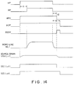
- Fig. 14 is a timing chart of an input signal HP to, and output signals RP and HSP from, the program control circuit PC, a potential at the word line WL1, a cell source/drain potential, and the output signals SSI(1+1) and SDI(1+1) of the block erase circuit BE(1+1).
- the input signal HP is a program signal which takes a level "H" when a program instruction is supplied to the memory device.
- the signal RP is a signal for driving a program potential raising circuit, which signal rises at a time delayed by a predetermined time t1 from a rise of the input signal HP, and falls simultaneously with a fall of the input signal HP.
- the signal HPS is a signal for driving the block erase circuit BEi and the stress moderating circuit SE, which signals rises simultaneously with a rise of the input signal HP, and falls at a time delayed by a predetermined time t2 from a fall of the input signal HP.
- the signal HCP takes a level "H" from the start of the program operation to when the voltages applied to the word line WL1, data line DL1, and source line are discharged, rises simultaneously with a rise of the signal HP, and falls at a time delayed by a predetermined time t3 from a fall of the signal HP.
- the signal RSTP is a pulse signal which is outputted during the period from when the signal HPS falls upon reception of a discharge signal of the data line DL11 at the end of the program operation to when the data line DL11 is completely discharged.
- the delay times t1, t2, and t3 are set as t3 ⁇ t1 > t2.
- the word line WL1 is controlled by the signal RP such that it rises and falls synchronously with the signal RP.
- the charge/discharge of the source line and data line DL11 is controlled by the signal HPS, and is connected to and disconnected from the stress moderating circuit SE via the transistor TUS(1+1) to the gate of which the signal SSI(1) is applied.
- the equalization between the source line SL(1+1) and data lines DL1(1+1) to DL n (1+1) is performed during the period from the start to end of the program operation.
- the equalization signal SDI(1+1) changes synchronously with the signal HCP.
- Fig. 15 shows an example of the program control circuit PC shown in Fig. 13.
- the program control circuit PC outputs the signals HPS, RP, HCP, and RSTP respectively shown in Fig. 14.
- a delay circuit DC1 sets the delay time t1 and t3
- another delay circuit DC2 sets the delay time t2.
- Fig. 16 shows an example of the block erase circuit BEi shown in Fig. 13.
- SI represents a signal from the decoder for selecting a block.
- HPS is a signal outputted from the program control circuit PC, which takes a level "H” only during the program operation.
- RE is a signal outputted from the erase control circuit EC, which takes a level "H” only during the erase operation.
- Charging the source line SL is performed by a transistor T104 to which an output node nB of a level shifter logic circuit is connected.
- the level shifter logic circuit is constructed of elements I100, I109, NR100, T100 to T103, and I102.
- Discharging the source line SL is performed by a logic circuit having elements ND100, I101, and NR101, a transistor T105 connected to an output node nC of the logic circuit, an inverter I103 whose input is connected to the node nC, and a transistor T112 to the gate of which an output node nG of a source potential detecting circuit is connected, the source potential detecting circuit being constructed of transistors T106 to T111.
- the node nC and node nG take a level "H"
- the transistors T105 and T112 turn on, so the source line SL is discharged.
- a transistor having a small discharge capability is used as the transistor T105, and a transistor having a large discharge capability is used as the transistor T112.
- a logic circuit constructed of elements I104 to I108, C100 to C103, and NR102 is a delay circuit for setting the timing of a signal for equalizing the source line SL and data line DL.
- Table 4 shows main node voltages at respective signal lines in a selected block and non-selected block during the program, the erase and read operations.
- V CC is 5 V
- V PP is 12 V.
- the source line SL is then connected to the stress moderating circuit and set to a potential determined by the stress moderating circuit SE.
- the operation of the stress moderating circuit SE starts at the same time when the source line SL and data line DL are equalized.
- the source/drain junction capacity is fairly large as compared with the capacity of the equalizing transistor TEQ. Therefore, it takes a long time to charge the source line SL and data line DL, so that the potential starts rising under the condition that there is no potential difference between the source line SL and data line DL.
- HPS becomes "L". Therefore, the discharge transistor T105 first turns on to start discharging the source line SL and data line DL.
- the node nG As the potential of the source line SL lowers and becomes equal to or less than the threshold value V th of the transistor T111, the node nG is gradually charged. After a predetermined time lapse, the discharge transistor T112 also turns on so that the source line SL is sufficiently discharged. In this example, charging the node nG is controlled by the D-type transistor T107.
- Fig. 17 shows another example of the block erase circuit BE.
- the equalizing signal SDI for the source and data lines is generated not by a delay circuit but by a latch circuit.
- the signal timings are the same as those of the circuit shown in Fig. 16.
- like elements to those shown in Fig. 16 are represented by using identical reference numerals.
- Fig. 18 shows another example of the block erase circuit BE.
- the source line SL is discharged not by feeding back the source potential but by using a delay circuit having a predetermined delay time.
- the signal timings are set in the same manner as shown in Fig. 16.
- like elements to those shown in Fig. 17 are represented by using identical reference numerals.
- Fig. 19 shows an example of the stress moderating circuit SE shown in Fig. 13.
- Transistors T400 to T405 constitute a constant voltage circuit CCc for setting the signal GSE.
- Transistors T406 and T407 constitute a charge circuit CC a
- transistors T411 and T412 constitute another charge circuit CC b .
- a transistor T413 functions as a discharge transistor.
- Transistors T408 to T410 constitute a feedback circuit FBC for controlling the gate potential of the discharge transistor T413.
- a transistor T414 functions as a reset transistor.
- This circuit SE sets the stress moderating potential GES to about 2 V during the program operation, and to 0 V during the operations except the program operation.
- HPSB becomes "L”
- the constant voltage circuit is set up and a node nH is set to a predetermined voltage.
- the transistors T407 and T410 turn on to start charging the GSE.
- GSE rises to the predetermined value
- the charge circuit CC a stops its charging, and the charge circuit CC b flows a current determined by a ratio of the discharge transistor T413 and the charge circuit CC b in the manner described hereinbelow.
- the feedback circuit FBC lowers gm of the transistor T409 such that the node nK is set nearly to 0 V at the charge start period, and then set to an optional potential Va ( ⁇ V CC : supply voltage) when GSE reaches the predetermined voltage value.
- the discharge transistor T413 turns off during the charge start period because the gate node nK is set nearly to 0 V. However, as GSE rises, it starts discharging and sets GSE to the predetermined potential in accordance with the ratio of the discharge transistor T413 to the charge circuit CC b .
- the potential of GSE is determined in accordance with the potential at the node nH of the constant voltage circuit and the threshold values V th of the transistors T407 and T410, and is set to V nH - V th where V nH is a potential at the node nH.
- I-type transistors V th is nearly 0 V
- GSE is set easily to any potential within a range from 1 V to 3 V.
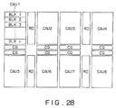
- the array of 4 M bit capacity for example is divided into two cell array units CAU1 and CAU2 disposed on opposite sides of a row decoder RD.
- the cell array unit CAU1 is divided into eight blocks BLC1 to BLC8, and the cell array unit CAU2 is divided into eight blocks BLC9 to BLC16.
- the array of 4 M bit capacity for example is divided into four cell array units CAU1 to CAU4, CAU1 and CAU2 being disposed on opposite sides of a row decoder RD1, and CAU3 and CAU4 being disposed on opposite sides of a row decoder RD2.
- the cell array units CAU1 to CAU4 are divided into four blocks BLC1 to BLC4, BLC5 to BLC8, BLC9 to BLC12, and BLC13 to BLC16, respectively.
- the junction capacity per one block can be considered to be 800 pF. Therefore, the charge/discharge capacity of the stress moderating circuit for the cell array of Fig. 20A is 5600 pF, and that for the cell array of Fig. 20B is 2400 pF.
- the dimension W (channel width) of a charge transistor In order to charge the non-selected block to 2 V in 200 ns, it is required to set the dimension W (channel width) of a charge transistor to 3000 to 5000 ⁇ m. therefore, a peak current is about 22 mA for the two-divided cell array, and about 14 mA for the four-divided cell array.
- the source potential at 2 V is discharged by using such a discharge transistor, the discharge time becomes 100 ns or shorter and the peak current becomes about 600 mA for the two-divided cell array, and about 220 mA for the four-divided cell array.
- the type of cell array division considerably influences current consumption.
- the current consumption of the two-divided cell array of Fig. 20A is 1.5 to 2.5 times as large as that of the four-divided cell array of Fig. 20B.
- the peak current is suppressed to about 10 mA or less by using a D-type charge transistor.
- first and second transistors having small and large discharge capabilities are used. Only the first discharge transistor with a small discharge capability is used during the discharge start period. Thereafter, the first and second discharge transistors with small and large discharge capabilities are used at the same time. In this manner, the peak current per one block is suppressed to about 2 mA or less.
- a potential is set without allowing a cell current to flow in a non-selected cell during the erase operation, thereby preventing malfunction of the non-selected cell.
- the source line SL and data line DL are equalized prior to applying an erase mode potential to the source line SL and word line WL.
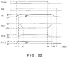
- FIG. 21 The conceptual diagram illustrating such an embodiment of the present invention is shown in Fig. 21, and its timing chart is shown in Fig. 22.
- an erase signal Erase becomes "H" level at time t1.
- an output EQ of a source bias circuit SBC becomes "H” level.
- equalizing transistors TEQ1 and TEQ2 turn on to connect together a source line SL and data lines DL1 and DL2.
- the potential VS of a cell source takes the same potential (e.g., 5 V) as that of the cell drain (data line DL1, DL2).
- a selected word line e.g., WL2 are set to predetermined potentials.
- the selected word line WL1 is set to -10 V
- the non-selected word line WL2 is set to 5 V( at time t3).
- the important points in setting such voltages are that the voltages of the word lines WL1 and WL2 are set after completely equalizing the potentials of the source and drain, and that a cell current is not allowed to flow while charging the word line WL2 of the non-selected cell to 5 V.
- Table 5 shows examples of setting voltages in various operation modes. While referring to Table 5, there will be described examples of the row decoder RD, negative bias circuit NBC, and source bias circuit SBC, respectively shown in Fig. 21.
- Figs. 23A to 25 show circuit portions of the row decoder RD.
- Fig. 23A shows a circuit which generates a potential of -10 V to be applied to a selected word line during the erase operation.
- a NAND gate at the input side of the circuit of Fig. 23A is applied with signals RA, RB, and RC all being 5 V outputted from a pre-decoder to which an address is inputted.
- the circuit of Fig. 23A operates as illustrated to output -10 V as an output WL.
- the operation of the circuit of Fig. 23A is well known by those skilled in the art, so the detailed description thereof is omitted.
- Fig. 23B shows a circuit which generates a potential of 5 V to be applied to a non-selected word line during the erase operation.
- a NAND gate at the input side is applied with three signals RA, RB, and RC, at least one of which is 0 V.
- the circuit of Fig. 23B operates as illustrated to output 5 V as an output WL.
- Fig. 24A shows a circuit which generates a potential of 12 V to be applied to a selected word line during the program operation.
- a NAND gate at the input side is applied with signals all being 5 V.
- the circuit of Fig. 24A operates as illustrated to output 12 V as an output WL.
- Fig. 24B shows a circuit which generates a potential of 0 V to be applied to a non-selected word line during the program operation.
- a NAND gate at the input side is applied with three signals RA, RB, and RC, at least one of which is 0 V.
- the circuit of Fig. 24B operates as illustrated to output 0 V as an output WL.
- Fig. 25 shows a circuit which generates a potential of 5 V to be applied to a selected word line during the read operation.
- a NAND gate at the input side is applied with signals RA, RB, and RC all being 5 V.
- the circuit of Fig. 25 operates as illustrated to output 5 V as an output WL.
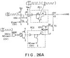
- Figs. 26A and 26B show examples of the negative bias circuit NBC.
- Fig. 26A shows a circuit which generates - 10 V as an output VMS during the erase operation. Specifically, during the erase operation, clocks OSC oscillating between 0 and 5 V as shown is applied to a transistor T1, and an erase signal (5 V) is applied to a transistor T2. As a result, an oscillation signal 0 to 12 V as shown appears at a node n1. This oscillation signal is inputted to a pump circuit PC1 at the next stage which then starts operating. An oscillation signal 0 to (-12 V) as shown appears at a node n2 of the pump circuit PC1.
- Fig. 26B is a circuit which generates 0 V as the VMS during the operations other than the erase operation.
- the circuit operates in the manner different from that shown in Fig. 26A in that an erase signal (0 V) is inputted to a transistor T2, and a non-erase signal (5 V) is inputted to the input terminal of a NAND gate.
- a voltage lowering pump circuit PC1 does not operate.
- An oscillation signal oscillating between 0 and 5 V as shown appears at a node n5.
- a pump circuit PC2 therefore starts operating.
- An oscillation signal oscillating between 0 and (-5 V) appears at a node n6 in the pump circuit PC2.
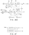
- Fig. 27 shows an example of the source bias circuit SBC.
- An output V s takes 5 V only during the erase operation, and takes 0 V during the program and read operations.
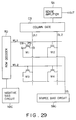
- Fig. 28 is a diagram for realizing such a method.
- a cell array is divided into eight cell array units SAU1 to SAU8.
- Each cell array unit SAUi is divided into n blocks BLK1 to BLKn.
- RD represents a row decoder
- CG represents a column decoder.
- one of the eight cell array units is selected to drive word lines, source lines, and data lines in only the selected unit. In this manner, power required for charge/discharge can be reduced.
Abstract
Description
- The present invention relates to a non-volatile semiconductor memory, and more particularly to a non-volatile semiconductor memory having a plurality block of non-volatile memory cells of two-layered structure, capable of altering data in units of block.
- All-bit flash erase type memories have drawn attention as electrically erasable, programmable read-only memories (E²PROM). Recent requirements for such memories are to provide a function of altering data in each of a plurality of memory blocks in units of block. For example, a 4 M bit device is divided into 16 blocks each having 32 K bytes or into 4 blocks each having 256 K bytes, and data erasure is required to be performed on the block unit basis. With such block division of a cell array, cells in a plurality of different blocks are connected to the same word line or data line. Therefore, repeating write/erase of a particular block may apply stress to cells in other non-selected blocks.
- The degree of such stress will be discussed for cells of two-layered structure. In the case of cells of two-layered structure used in a flash type E²PROM, data write is performed in a manner similar to EPROM. Namely, a control gate is applied with VCG = 12 V, a drain with VD = 6 V, and a source with VS = 0 V. In this state, hot electrons generated by an avalanche effect are injected to the floating gate. For data erase, the control gate is applied with VCG = 0 V, the source with VS = 12 V. In this state, electrons are taken out of the floating gate as F-N tunnel current between the floating gate and source.
- The characteristic structure of such a cell resides in that the gate oxide film under the floating gate is about 100 angstroms thinner than that of an EPROM cell because a tunnel current flows between the floating gate and source during data erase, and that the superposing area of the source n⁺ region and the floating gate is made wider than that of EPROM.
- In a cell array having a plurality of blocks comprised by cells of such structure, stress applied to a cell in an erase state or write state in a non-selected block is shown in Table 1. A cell in an erase state in a non-selected block connected to a selected word line is applied to an electric field of about 7.5 MV/cm between its floating gate and source, and a cell in a write state in a non-selected block connected to a selected data line is applied to an electric field of about 6.5 MV/cm between its floating gate and drain.

- Next, there will be discussed the time period while stress is applied to a cell in a non-selected block during data erase or data write. Consider a 4 M bit device divided into blocks at intervals of 32 K bytes in the data line direction. Assuming that cells in a block are subject to write/erase as many as 10⁵ times with a write time of 10 µs and write occurrence frequency of 25 times for each cell, a cell in a non-selected block is applied with VCG = 12 V during the total time period of 800 sec. Stress of 7.5 MV/cm is therefore applied between the floating gate and source during the time period 800 sec, inevitably leading to write error. As an alternate, consider a 4 M bit device divided into blocks at intervals of 32 K bytes in the word line direction, a cell in a non-selected block is applied with 6 V at its drain during the total time period 6400 sec. Stress of 6.5 MV/cm is therefore applied between the floating gate and drain during the time period 6400 sec, inevitably leading to erase error.
- As described above, a conventional device is associated with the problem that as data write and erase are effected to a selected block, data write error and erase error may occur at non-selected blocks.
- In a conventional data erase scheme, electrons accumulated in a floating gate FG are emitted toward the source by applying a high voltage to the cell source, as discussed previously. With this scheme, it is unable to use a source voltage equal to or higher than the breakdown voltage of a source junction, there arises some restriction that cell sources are required to be formed separately in order to allow block erase (simultaneous erase of a plurality of cells contained within one block). Another scheme using a negative voltage has been considered which can erase data without applying a high voltage to the cell source. An apparatus performing such scheme is conceptually shown in Fig. 29, and timings of waveforms used by the apparatus are shown in Fig. 30. Table 2 shows examples of voltages set to cells at different modes.
Table 2 Mode Cell WL DL Source Erase Selected Cell -10 V 3 V 5 V Non-selected Cell 5 V 3 V 5 V Program Selected Cell 12 V 6 V 0 V Read Selected Cell 5 V 1 V 0 V - This scheme is characterized in that a plurality of memory cells connected to one selected word line can be erased at the same time. It is now assumed that a word line WL₁ is selected and another word line WL₂ is not selected in a data erase mode. Specifically, the selected word line WL₁ is applied with a voltage VWL₁ of -10 V, the non-selected word line WL₂ is applied with a voltage VWL₂ of 5 V, a source voltage VS is set to 5 V, and data lines DL₁ and DL₂ are set to a floating state. In this state, memory cells M1 and M2 enter an erase state, and memory cells M3 and M4 enter a non-erase state. In a program mode (in a data write mode), hot electrons are injected into a floating gate FG. In a read mode, a sense amplifier judges whether a selected cell is being turned on (a cell current flows) or off (a cell current will not flow).
- The above-described scheme has the following problems. At the non-selected cells M3 and M4 in the erase mode, WL₂ is set to 5 V, VS is set to 5 V, and DL₁ and DL₂ enter the floating state. As a result, the data lines DL₁ and DL₂ are charged via the non-selected cells M3 and M4 up to (5 V - Vth) where Vth is a cell threshold value. A cell current for charging the data lines DL₁ and DL₂ flows in the non-selected cells M3 and M4 during the time period from t₁ to t₂, therefore leading to a possibility of write error at the non-selected cells M3 and M4. Also in the end of erase mode, electric charges used for charging the data lines DL₁ and DL₂ are discharged so that a cell current will flow during the time period from t₃ to t₄, leading to a possibility of write error. In addition, if charge/discharge relative to the source and word lines is carried out rapidly, a peak current will flow which may break wiring material.
- It is an object of the present invention to provide a non-volatile semiconductor memory capable of preventing malfunction such as write error, erase error and the like, during the data write and data erase.
- It is another object of the present invention to provide a non-volatile semiconductor memory capable of preventing malfunction of a non-selected memory cell upon data write or erase for an optional number of memory cells selected from a plurality of memory cells.
- It is a further object of the present invention to provide a non-volatile semiconductor memory wherein the memory cell are divided into a plurality of blocks each having a plurality of memory cells, data can be altered on the block unit basis, and malfunction of a cell in a non-selected block can be prevented even if data in a cell in a selected block is written or erased.
- A memory cell array is divided into a plurality of blocks. In altering data for a block (selected block), a moderating voltage is applied to the source or control gate of a memory cell in another block (non-selected block) to moderate stress between the floating gate and source/drain, thereby preventing write error and erase error.
- In the program operation, the source and drain of a memory cell in the non-selected block are equalized to moderate an electric field between the control gate and source/drain and not to flow a channel current, thereby preventing write error.
- In carrying out a negative voltage erase method, prior to setting the source line and word line of a cell in a non-selected block to an erase voltage, the source and data lines are equalized. The equalization operation is released after the erase operation, thereby preventing malfunction of a non-selected cell.
- Fig. 1 is a diagram showing the overall arrangement of an embodiment according to the present invention.
- Fig. 2 is a circuit diagram showing the details of a portion of the embodiment shown in Fig. 1.
- Figs. 3 to 7 are circuit diagrams showing examples of the block erase circuit of the embodiment shown in Fig. 1.
- Fig. 8 is a circuit diagram showing the details of the column gate section.
- Fig. 9 is a circuit diagram showing the main portion of the row decoder.
- Fig. 10 is a graph showing the characteristics of a memory cell in a non-selected block.
- Fig. 11 is a diagram showing the overall arrangement of another embodiment according to the present invention.
- Fig. 12 is a circuit diagram showing the details of a portion of the embodiment shown in Fig. 11.
- Fig. 13 is a diagram showing the overall arrangement of another embodiment according to the present invention.
- Fig. 14 is a timing chart explaining the operation of the embodiment shown in Fig. 13.
- Fig. 15 is a circuit diagram of the program control circuit shown in Fig. 13.
- Fig. 16 is a circuit diagram showing an example of the block erase circuit shown in Fig. 13.
- Fig. 17 is a circuit diagram showing another example of the block erase circuit.
- Fig. 18 is a circuit diagram showing another example of the block erase circuit.
- Fig. 19 is a circuit diagram of a stress moderating circuit.
- Figs. 20A and 20B are diagrams explaining the relationship between cell array division and current consumption.
- Fig. 21 is a conceptual view showing another embodiment of the present invention.
- Fig. 22 is a timing chart explaining the operation of the embodiment shown in Fig. 21.
- Figs. 23A and 23B illustrate the states of a selected word line and non-selected word line shown in Fig. 21 during an erase mode.
- Figs. 24A and 24B illustrate the states of a selected word line and non-selected word line shown in Fig. 21 during the program mode.
- Fig. 25 illustrates the state of the row decoder shown in Fig. 21 during the read mode.
- Figs. 26A and 26B illustrate the state of the negative bias circuit shown in Fig. 21 during the erase mode and other modes.
- Fig. 27 is a circuit diagram of the source bias circuit shown in Fig. 21.
- Fig. 28 is a conceptual diagram showing the overall arrangement of another embodiment according to the present invention.
- Fig. 29 is a conceptual diagram of a conventional memory device.
- Fig. 30 is a timing chart explaining the operation of the conventional memory device.
- Fig. 1 shows a device whose memory cell array is divided into sixteen blocks in the data line direction according to the first embodiment. The
memory cell array 1 is divided into sixteenblocks 2 each provided with a block erasecircuit 3. In Fig. 1,reference numeral 5 represents a row decoder,reference numeral 6 represents a column decoder, andreference numeral 7 represents a row pre-decoder. The details of eachblock 2 are shown in Fig. 2. As seen from Fig. 2, each block erasecircuit 3 is commonly connected to the sources of cells CXY in eachblock 2. Cells commonly connected to one data line DLαβ are located within the same block. Cells commonly connected to one word line WLi are located over a plurality of blocks. - A data alteration operation of one block of the device constructed as above will be described below.
- In the erase sequence for cells of two-layered structure described above, in order to prevent a read error of a cell due to transformation to the depletion type of a cell to be caused by over erase, all cells in a subject block are first written with data and then erased at the same time. In a write mode, a sequence similar to the case of EPROM is executed. In other words, for the data alteration, a write operation is carried out twice. In this case, stress is applied to the control gates of cells in non-selected blocks connected to the same word line of the block to be altered.
- In this embodiment, in order to moderate an electric field between the floating gates and sources of cells in an erase state in non-selected blocks, a predetermined potential (moderating potential) is applied to the cell sources. For example, if a potential of 2 V is applied to a cell source, the electric field between the floating gate and source becomes about 5 MV/cm which moderates the electric field by about 2.5 MV/cm as compared with about 7.5 MV/cm when 0 V is applied to the cell source.
- Fig. 3 is an example of a circuit diagram of the block erase
circuit 3 according to the present invention. This circuit is constructed of ablock selecting unit 11, alevel shifter 12, a charge transistor T116, discharge transistors T120 and T121, adelay circuit 13, and a non-selectedblock bias circuit 14. The block selecting circuit has a NOR gate NR100 calculating a NOR between an address selection signal BS and a signal NErase, the address selection signal BS being supplied from a NAND gate NA100 to which a block selection address BSA is inputted. Thelevel shifter 12 is constructed of transistors T110 to T115 and an inverter I110. The charge transistor T116 is used for charging the selectedblock 2. The discharge transistors T120 and T121 are used for discharging electric charges from the cell sources during the time period except for the erase operation. Thedelay circuit 13 is used for controlling the timing of discharge, and is constructed of inverters I120 to I124, and a NAND gate NA120. The non-selectedblock bias circuit 14 is constructed of transistors T130 to T132, and resistors R130 and R131. - Next, the operation of the
circuit 3 shown in Fig. 3 will be described. - In the erase mode, the block erase
circuit 3 of ablock 2 selected by an address takes a state that an output BS of NA100 becomes "L", the signal NErase becomes "L", and an output EA of NR100 becomes "H". As a result, an output EAG of thelevel shifter 12 becomes "L" which is applied to the charge P-ch transistor T116, so that VPP = 12 V is applied to the cell sources CS. - At this time, the discharge transistors T120 and T121 turn off, the gates of which are applied with NErase and its delayed signal, respectively. In the non-selected
block bias circuit 14, the transistor T130 turns on and the transistor T131 turns off, respectively upon reception of NErase = "L". As a result, current flows from the transistor T130 to the resistors R130 and R131 and to ground, setting a node NEG to an intermediate potential. Although the cell sources are charged to VPP, the transistor T132 has a low gate voltage so that it turns off. - The block erase
circuit 3 of anon-selected block 2 takes a state that the output BS of the decoder NA100 becomes "H" upon reception of an address signal, the output EA of NR100 for driving thelevel shifter 12 becomes "L", the gate node EAG of the charge P-ch transistor T116 becomes "H" (= VPP), and the charge transistor T116 turns off. In the non-selectedblock bias circuit 14, the signal NErase becomes "L", the transistor T130 turns on, the transistor T131 turns off, and current flows from T130 to the resistors R130 and R131 and to ground. Therefore, the node NEG between R131 and R131 takes a potential determined by the resistances of T130, R130, and R131. The cell sources are therefore charged through T132 and set to the potential of NEG - VTH (T132). For example, assuming that NEG is 3 V, and VTH of T132 is 1 V, then the cell sources are set to 2 V. At this time, similar to the case of the block erasecircuit 3 connected to the selected block, the discharge transistors T120 and T121 turn off. - After the erase operation, the signal NErase becomes "H". For the selected
block 2, the charge transistor T116 turns off, and for thenon-selected block 2, the transistor T130 turns off, the transistor T131 turns on, and the charge transistor T132 turns off. Also with NErase = "H", the transistor T120 turns on to start discharging the cell sources. The gate of the transistor T121 becomes "H" after a predetermined time delay set by thedelay circuit 13, to discharge the transistor T121. The reason why two transistors T120 and T121 are used for discharge is that an excessive peak current will flow if discharge is performed by a transistor of large dimension, because the junction capacity of the cell source region is large. The dimension of the transistor T120 is set small to gradually discharge. After discharging to some degree and obtaining a lower potential, discharge is further performed by the transistor T121 whose dimension is set large. The reason why the dimension of the transistor T121 is set large is to prevent the cell sources SC from floating above 0 V (ground) during a read or program mode. Particularly in the program mode, a current of several mA flows so that it is necessary to set W to about several hundreds to 1000 µm. - During the program, read, and stand-by mode, the signal NErase becomes "H". Therefore, the charge transistors T116 and T132 turn off, and the discharge transistors T120 and T121 turn on, setting the cell sources CS to a ground potential (= 0 V).
- The node potentials in respective modes are shown in Table 3.

- Other examples of the non-selected block bias circuit of the block erase
circuit 3 are shown in Figs. 4 to 7. - In the circuit shown in Fig. 4, the resistors R130 and R131 shown in Fig. 3 are replaced by transistors. Namely, the resistor R130 is replaced by transistors T141 to T144, and the resistor R131 is replaced by transistors T145 and T146. Basically, the gate potential NEG of a charge transistor T148 is determined by a division ratio of resistors.
- In the circuit shown in Fig. 5, the gate potential NEG of a charge transistor T155 is determined by the values VTH of transistors T152 and T153. With this circuit arrangement, the node NEG is set to 2 VTH and the cell sources are set to about VTH level.
- In the circuit shown in Fig. 6, the potential at the cell sources CS is determined by VTH of a D-type transistor T161. In the erase operation, the signal NErase becomes "L", a transistor T160 turns on, and the gate of the transistor T161 becomes "L". As a result, the cell sources in a non-selected block are charged to a value VTH of the D-type transistor T161, i.e., to about 1 to 2 V.
- The circuit shown in Fig. 7 uses a VTH drop (potential drop) of an E-type transistor T170. With NErase = "L", a transistor T171 turns on and the VTH drop level of T170 is applied to the cell sources CS. The circuits shown in Figs. 6 and 7 save power because current will not flow always as in the circuits shown in Figs. 3 to 5.
- The above-described circuits turn off upon reception of NErase + "H" during the program, read, and stand-by modes except the erase mode.
- Fig. 8 shows the structure of the column gate. Fig. 8 corresponding to Fig. 1 shows the column structure of one block, a row decoder buffer, a word line, and cells C₁₁₁ to C1m1 connected to the word line. This device is obtained, for example, by dividing a 4 M bit cell array into sixteen blocks in the data line direction at intervals of 32 K bytes. One block has 128 data lines for 8 I/O units each I/O assigned 16 data lines. One byte is selected by one of column signals h1 to h16. Each block is selected by one of column signals s1 to s16.
- In Fig. 8, T200 to T207 represent column gate transistors for selecting a block, and T210 to T287 represent column gate transistors selected by the column signal h1 to h16.
- Fig. 9 shows the structure of the
row decoder 5. - In Fig. 9, MD represents a main decoder having a plurality of transistors T350 to T355 and selected by outputs RAi, RBi, and RCi from the row pre-decoder, T300, T310, T320, T330, T340 to T343 represent transfer gates selected by outputs RDRi and RDLi from the row pre-decoder, T300', T310', T320', and T330' represent charge transistors, T301 to T303, T311 to T313, T321 to T323, and T331 to T333 represent feedback-type inverters. A circuit CIR at the left side of Fig. 9 has the same structure as the circuit CIR at the right side.
- If a word line WL₁ for example is to be selected, the main decoder MD selected by the outputs RAi, RBi, and RCi takes a state of RA = RB = RC = "H", so that a node MAIN becomes "L". RDR₁ for selecting the word line WL₁ becomes "H", and NRDR₁ becomes "L". Other RDR₂ to RDR₄ become "L", and other NRDR₂ to NRDR₄ become "H". As a result, the transistor T302 turns on and the transistor T303 turns off, so the word line WL₁ takes an SW potential. At this time, the transistors T312, T322, and T332 turn off T313, T323, and T333 turn on, so the other word lines WL₂ to WL₄ take a ground level.
- In the memory device having divided blocks according to the embodiment of the present invention, first to
eighth blocks 2 and ninth to sixteenthblocks 2 are grouped on opposite sides of therow decoder 5 as shown in Fig. 1. The right transfer gate RDRi executes a logical calculation with a block selecting column signal Si to drive only the right word line connected to the selected block. Similarly, the left transfer gate RDLi executes a logical calculation with the block selecting column signal Si to drive only the left word line connected to the selected block. - Fig. 10 is a graph showing the relationship between time duration of stress applied to the control gate of an erased cell in a non-selected block and a change in cell VTH. The cell source is assumed to be set to 0 V. As the control gate stress time period becomes long, the cell VTH rises. This rise is dependent upon the control gate potential. For VCG = 13 V, a large rise is observed at about 100 sec. For VCG = 9 V on the other hand, a rapid rise will not be observed up to 1000 sec. The above cases are observed when setting the cell source to 0 V. If the cell source is set to 2 V, the characteristics obtained at the electric field between the floating gate and source corresponding to VCG = 13 V are substantially equal to the characteristics obtained at the electric field corresponding to VCG = 9 V and cell source set to 0 V.
- Assuming that the coupling ratio Ccf is 0.5 between the control gate and floating gate and the coupling ratio Csf is 0.1 between the source and floating gate, the floating gate potential VFG at the cell source set to 0 V and VCG = 13 V becomes:

and so the electric field Esf between the source and floating gate becomes 6.5 MV/cm. At the cell source set to 0 V and VCG = 9 V, then VFG becomes 4.5 V and Esf becomes 4.5 MV/cm. If the cell source is set to 2 V and VCG = 13 V, then the floating gate potential VFG becomes:


and so Esf = 6.7 - 2 = 4.7 MV/cm. - As described above, by raising the cell source potential of a non-selected block by about 2 V, it is possible to sufficiently suppress the variation of the VTH of a cell in an erase state.
- The terms VTH0 and VTHMax are herein introduced, the term VTH0 being a VTH of a cell in an erase state without no stress, and the term VTHMax being a limit VTH of a cell providing no access time delay and no read error.
- If there is provided no effective countermeasure for a cell source, the cell VTH becomes VTHMax at VCG = 13 V and in stress time period of about several hundreds sec. In contrast, if a countermeasure for raising a potential at a cell source, the cell VTH will not reach VTHMax even at VCG = 13 V and in stress time period of about 1000 sec or longer, by raising to Vs = 2 V which corresponds to a drop of VCG = 4 V.
- If data alteration is repeated 10⁵ times to a particular block of a memory device divided as shown in Fig. 1, the stress time period of cells in a non-selected block is about 800 sec, enabling to prevent malfunction to be caused by stress.
- Next, the second embodiment will be described with reference to Fig. 11.
- In this embodiment, different from the first embodiment, a memory cell array is divided into blocks in the word line direction. Similar to the first embodiment, a block erase
circuit 3 is provided at each block. The layout of cells is shown in Fig. 12. Cells C commonly connected to a word line WL are located within the same block. On the other hand, cells C commonly connected to a data line CL are located over a plurality of blocks. With such an arrangement, one data line CL is commonly connected to all corresponding cells in first to sixteenth blocks. Arow decoder 5 selects aparticular block 2 by applying a high potential to a word line WL of theblock 2, while raising the potentials of other word lines WL in non-selected blocks to a potential, for example, a potential half that of the word line WL of the selected block. Such a circuit for raising the potential of word lines of non-selected blocks may use any general circuit for raising a word line potential. - In the present embodiment, stress can be moderated by setting the control gate of a cell in a non-selected block to VCG = 5 V.
- A cell in a write state in a non-selected block takes a value 5.6 MV/cm at VCG = 0 V and


- The following advantageous effects can be obtained by the present embodiment.
- Stress applied to a cell in a non-selected block can be moderated even in the case of a flash-type E²PROM cell array divided into blocks for data alteration on the block unit basis. For example, even if data alteration is repeated 10⁵ times with respect to a particular block, the VTH variation of a cell in a non-selected block can be sufficiently suppressed. The time period required for a cell to reach VTHMax at which a malfunction may occur, is elongated several ten times at VCG = 13 V for example, providing an ample margin during 10⁵ write/erase cycles.
- In addition to a conventional all bit flash erase operation, an erase on the block unit basis is possible, providing value-added performance and an increased number of write/erase cycles with high reliability.
- Next, another embodiment will be described with reference to Figs. 13 to 19B. In this embodiment shown therein, during a program mode, the source and drain of a memory cell in a non-selected block are biased to the same potential at the same time to moderate the electric field between the control gate and source/drain and not to flow a channel current, thereby preventing write error and improving the reliability.
- Fig. 13 shows the overall structure of this embodiment. In Fig. 13, a cell array is divided into a plurality of blocks 2i (2₁, 2₂, ...) in the data line DLi direction. This memory device is provided with a stress moderating circuit SE shared by all blocks, and block erase circuits BE₁, BE₂, ... connected to corresponding source lines SL₁, SL₂, ... of respective blocks. Consider now one block 21, the source line SL₁ is connected to data lines DL₁₁ to DLn1 via transfer gates TEQ₁₁ to TEQn1 to the gates of which an output signal SDI(1) from the block erase circuit BE₁ is applied. An output (GSE) of the stress moderating circuit SE is connected to the source line SL₁ via a transfer gate TUS(1) to the gate of which an output signal SSI(1) of the block erase circuit BE₁ is applied. The other blocks are constructed in substantially the same as the block 21. In Fig. 13, PC represents a program control circuit, PHC represents a write potential raising circuit, CG represents a column gate, RD represents a row decoder, and EC represents an erase control circuit.
- The operation of the memory device constructed as above will be described. It is assumed that the block 21 is selected and a cell C₁₁₁ is selected to write data therein. In other words, it is assumed that in this selected block 21, the selected word line WL₁ and data line DL₁₁ are connected to the write potential raising circuit PHC via the row decoder RD and column gate CG to write data in the selected cell Cn1. The output signals SDI(1) and SSI(1) of the block erase circuit BE₁ of the selected block 21 take a level "L", and the source line SL₁ is disconnected from the data line DL₁₁ and from the output (GSE) of the stress moderating circuit. In a non-selected block, e.g., block 2(1+1), the output signals SDI(1+1) and SSI(1+1) of the block erase circuit BE(1+1) take a level "H", so the transistors TEQ₁(1+1) to TEQn(1+1) and TUS(1+1) turn on. The source line SL(1+1) and data lines DL₁(1+1) to DLn(1+1) are connected to the stress moderating circuit SE. Accordingly, the source and drain of each cell are set to about 2 V set by the stress moderating circuit SE. In this manner, in all non-selected blocks, the electric field between the cell gate and source/drain of each cell on the selected word line WL₁ is moderated.
- Next, the timing for moderating stress in a non-selected block, e.g., block 2(1+1) will be described. In order to moderate gate stress of a cell in the non-selected block 2(1+1) during the write operation, it is necessary to raise the source/drain voltage VSD(1+1) prior to a rise of the word line WL₁, and to lower the source/drain voltage VSD(1+1) after a fall of the word line WL₁. As the timing for an equalizer, the source/drain is equalized prior to charging by the stress moderating circuit SE, and the equalization is released after completion of discharging the source/drain. Namely, in the program operation, an input HP to the program control circuit PC takes a level "H" to start the operation of a series of program-operation circuits. In the non-selected block 2(1+1), the output signals SDI(1+1) and SSI(1+1) take a level "H", and the transistors TEQ₁(1+1) to TEQn(1+1) and TUS(1+1) turn on. As a result, the source/drain is equalized and connected to the stress moderating circuit SE. At the same time, the stress moderating circuit SE starts operating to charge the source/drain to a predetermined potential. The word line WL₁ potential rises after the source/drain potential is raised to a predetermined value. At the end of the program operation, after the word line WL₁ potential lowers, the output SSI(1+1) of the block erase circuit BE(1+1) takes a level "L". Then, the transistor TUS(1+1) turns off to disconnect the stress moderating circuit SE and the source/drain. After the source/drain potential lowers, the output SDI(1) of the block erase circuit BE(1+1) takes a level "L", so that the transistors TEQ₁(1+1) to TEQn(1+1) turn off to release the equalization of the source/drain. With the timings set as described above, the electric field between the control gate and source/drain can be moderated without flowing a channel current through the non-selected cell, while sufficiently suppressing an occurrence of write error.
- Fig. 14 is a timing chart of an input signal HP to, and output signals RP and HSP from, the program control circuit PC, a potential at the word line WL₁, a cell source/drain potential, and the output signals SSI(1+1) and SDI(1+1) of the block erase circuit BE(1+1). The input signal HP is a program signal which takes a level "H" when a program instruction is supplied to the memory device. The signal RP is a signal for driving a program potential raising circuit, which signal rises at a time delayed by a predetermined time t₁ from a rise of the input signal HP, and falls simultaneously with a fall of the input signal HP. The signal HPS is a signal for driving the block erase circuit BEi and the stress moderating circuit SE, which signals rises simultaneously with a rise of the input signal HP, and falls at a time delayed by a predetermined time t₂ from a fall of the input signal HP. The signal HCP takes a level "H" from the start of the program operation to when the voltages applied to the word line WL₁, data line DL₁, and source line are discharged, rises simultaneously with a rise of the signal HP, and falls at a time delayed by a predetermined time t₃ from a fall of the signal HP. The signal RSTP is a pulse signal which is outputted during the period from when the signal HPS falls upon reception of a discharge signal of the data line DL₁₁ at the end of the program operation to when the data line DL₁₁ is completely discharged. In the above-described timings, the delay times t₁, t₂, and t₃ are set as t₃ ≧ t₁ > t₂. The word line WL₁ is controlled by the signal RP such that it rises and falls synchronously with the signal RP. The charge/discharge of the source line and data line DL₁₁ is controlled by the signal HPS, and is connected to and disconnected from the stress moderating circuit SE via the transistor TUS(1+1) to the gate of which the signal SSI(1) is applied. The equalization between the source line SL(1+1) and data lines DL₁(1+1) to DLn(1+1) is performed during the period from the start to end of the program operation. The equalization signal SDI(1+1) changes synchronously with the signal HCP.
- Fig. 15 shows an example of the program control circuit PC shown in Fig. 13. The program control circuit PC outputs the signals HPS, RP, HCP, and RSTP respectively shown in Fig. 14. In this example, a delay circuit DC₁ sets the delay time t₁ and t₃, and another delay circuit DC₂ sets the delay time t₂.
- Fig. 16 shows an example of the block erase circuit BEi shown in Fig. 13. SI represents a signal from the decoder for selecting a block. HPS is a signal outputted from the program control circuit PC, which takes a level "H" only during the program operation. RE is a signal outputted from the erase control circuit EC, which takes a level "H" only during the erase operation.
- The charge/discharge operation for the source line SL will be described below with reference to Fig. 16.
- Charging the source line SL is performed by a transistor T104 to which an output node nB of a level shifter logic circuit is connected. The level shifter logic circuit is constructed of elements I100, I109, NR100, T100 to T103, and I102. When the node nB takes a level "H", the transistor T104 turns off, and the source line SL will not be charged. When the node nB takes a level "L", the transistor T104 turns on, and the source line SL is charged. Discharging the source line SL is performed by a logic circuit having elements ND100, I101, and NR101, a transistor T105 connected to an output node nC of the logic circuit, an inverter I103 whose input is connected to the node nC, and a transistor T112 to the gate of which an output node nG of a source potential detecting circuit is connected, the source potential detecting circuit being constructed of transistors T106 to T111. When the node nC and node nG take a level "H", the transistors T105 and T112 turn on, so the source line SL is discharged. A transistor having a small discharge capability is used as the transistor T105, and a transistor having a large discharge capability is used as the transistor T112. The reason for this is to suppress a peak current at the time of discharging the source potential. With such an arrangement, the transistor T105 with a small discharge capability slowly discharges the source line SL during the discharge start period, and after the source potential lowers to some extent, the transistor T112 having a large discharge capability quickly discharges the source line SL. Furthermore, provision of the transistor with a large discharge capability is to suppress a rise of the source potential during the write and read operations. When the nodes nC and nG take a level "L", the transistors T105 and T112 turn off, so the source line will not be discharged. A logic circuit constructed of elements I104 to I108, C100 to C103, and NR102 is a delay circuit for setting the timing of a signal for equalizing the source line SL and data line DL.
- Table 4 shows main node voltages at respective signal lines in a selected block and non-selected block during the program, the erase and read operations. In this Table, it is assumed that VCC is 5 V, and VPP is 12 V.

- Next, the detailed operation at each mode will be described below.
- During the program operation, RE = "L" at all blocks. The node nB takes a level "H" so that the source line will not be charged from VPP. In the selected block, SI = "H" and the nodes nC and nG take a level "H". Therefore, the source line SL becomes a discharge state allowing to flow a sufficient program current (several hundred mA) through a selected cell. In the non-selected block, when SI = L, HSP becomes "H", the nodes nC and nG become L" so that the discharge transistors T105 and T112 turn off. At the same time, SSI and SDI become "H" so that the source line SL and data line DL are equalized. The source line SL is then connected to the stress moderating circuit and set to a potential determined by the stress moderating circuit SE. In this case, the operation of the stress moderating circuit SE starts at the same time when the source line SL and data line DL are equalized. The source/drain junction capacity is fairly large as compared with the capacity of the equalizing transistor TEQ. Therefore, it takes a long time to charge the source line SL and data line DL, so that the potential starts rising under the condition that there is no potential difference between the source line SL and data line DL. At the end of the program operation, HPS becomes "L". Therefore, the discharge transistor T105 first turns on to start discharging the source line SL and data line DL. As the potential of the source line SL lowers and becomes equal to or less than the threshold value Vth of the transistor T111, the node nG is gradually charged. After a predetermined time lapse, the discharge transistor T112 also turns on so that the source line SL is sufficiently discharged. In this example, charging the node nG is controlled by the D-type transistor T107.
- During the erase operation, HPS = "L". In the selected block at SI = "H", when RE becomes "H" at the start of the erase operation, the nodes nB, nC, and nG become "L" so that the source line SL is charged from VPP. When RE becomes "L" at the end of the erase operation, the nodes nB and nC become "H". Discharge starts first by the discharge transistor T105 with a small discharge capability, and after the source line SL potential becomes equal to or less than a predetermined value, the discharge transistor T112 with a large discharge capability also turns on. Discharge is therefore carried out by the two transistors T105 and T112. In a non-selected block at Si = "L", the nodes nB, nC, and nG become "H", and the source line SL is set to 0 V, disabling the erase operation.
- During the read and stand-by operations, RE = "L" and HPS = "L" so that the source line is set to 0 V.
- Fig. 17 shows another example of the block erase circuit BE. In this circuit, the equalizing signal SDI for the source and data lines is generated not by a delay circuit but by a latch circuit. The signal timings are the same as those of the circuit shown in Fig. 16. In Fig. 17, like elements to those shown in Fig. 16 are represented by using identical reference numerals.
- Fig. 18 shows another example of the block erase circuit BE. In this example, the source line SL is discharged not by feeding back the source potential but by using a delay circuit having a predetermined delay time. The signal timings are set in the same manner as shown in Fig. 16. In Fig. 18, like elements to those shown in Fig. 17 are represented by using identical reference numerals.
- Fig. 19 shows an example of the stress moderating circuit SE shown in Fig. 13. Transistors T400 to T405 constitute a constant voltage circuit CCc for setting the signal GSE. Transistors T406 and T407 constitute a charge circuit CCa, and transistors T411 and T412 constitute another charge circuit CCb. A transistor T413 functions as a discharge transistor. Transistors T408 to T410 constitute a feedback circuit FBC for controlling the gate potential of the discharge transistor T413. A transistor T414 functions as a reset transistor.
- The operation of the stress moderating circuit SE shown in Fig. 19 will be described below.
- This circuit SE sets the stress moderating potential GES to about 2 V during the program operation, and to 0 V during the operations except the program operation. When HPSB becomes "L", the constant voltage circuit is set up and a node nH is set to a predetermined voltage. In the charge circuits CCa and CCb, the transistors T407 and T410 turn on to start charging the GSE. When GSE rises to the predetermined value, the charge circuit CCa stops its charging, and the charge circuit CCb flows a current determined by a ratio of the discharge transistor T413 and the charge circuit CCb in the manner described hereinbelow. The feedback circuit FBC lowers gm of the transistor T409 such that the node nK is set nearly to 0 V at the charge start period, and then set to an optional potential Va (< VCC: supply voltage) when GSE reaches the predetermined voltage value. The discharge transistor T413 turns off during the charge start period because the gate node nK is set nearly to 0 V. However, as GSE rises, it starts discharging and sets GSE to the predetermined potential in accordance with the ratio of the discharge transistor T413 to the charge circuit CCb.
- In this circuit SE, the potential of GSE is determined in accordance with the potential at the node nH of the constant voltage circuit and the threshold values Vth of the transistors T407 and T410, and is set to VnH - Vth where VnH is a potential at the node nH. In this example, I-type transistors (Vth is nearly 0 V) are used as the transistors T407 and T410, so that the potential of GSE is set in accordance with the potential at the output node nH of the constant voltage circuit. In this manner, by changing the parameters of the constant voltage circuit CCc, GSE is set easily to any potential within a range from 1 V to 3 V.
- Next, there will be described the relationship between the type of cell array division and power consumption.
- In the cell array shown in Fig. 20A, the array of 4 M bit capacity for example is divided into two cell array units CAU1 and CAU2 disposed on opposite sides of a row decoder RD. The cell array unit CAU1 is divided into eight blocks BLC1 to BLC8, and the cell array unit CAU2 is divided into eight blocks BLC9 to BLC16. In the cell array shown in Fig. 20B, the array of 4 M bit capacity for example is divided into four cell array units CAU1 to CAU4, CAU1 and CAU2 being disposed on opposite sides of a row decoder RD1, and CAU3 and CAU4 being disposed on opposite sides of a row decoder RD2. The cell array units CAU1 to CAU4 are divided into four blocks BLC1 to BLC4, BLC5 to BLC8, BLC9 to BLC12, and BLC13 to BLC16, respectively.
- Only a selected cell array unit is driven and a non-selected cell array unit is set in a stand-by state. In this case, no stress is applied to the non-selected cell array unit. Therefore, it is not necessary to apply a stress moderating voltage to the non-selected cell array unit. It is sufficient that the moderating voltage is applied only to a non-selected block in the selected cell array unit. Consider now charge/discharge associated with a stress moderating voltage at a non-selected block in the selected cell array unit. In the case of the two-divided cell array shown in Fig. 20A, there are seven non-selected blocks, and in the case of the four-divided cell array shown in Fig. 20B, there are three non-selected blocks. The junction capacity per one block can be considered to be 800 pF. Therefore, the charge/discharge capacity of the stress moderating circuit for the cell array of Fig. 20A is 5600 pF, and that for the cell array of Fig. 20B is 2400 pF. In order to charge the non-selected block to 2 V in 200 ns, it is required to set the dimension W (channel width) of a charge transistor to 3000 to 5000 µm. therefore, a peak current is about 22 mA for the two-divided cell array, and about 14 mA for the four-divided cell array. In order not to float the source potential in excess of 0.1 V or more even if a program current about 1 mA flows during the program operation, it is required to set the dimension W of the discharge transistor to 800 µm or more. If the source potential at 2 V is discharged by using such a discharge transistor, the discharge time becomes 100 ns or shorter and the peak current becomes about 600 mA for the two-divided cell array, and about 220 mA for the four-divided cell array. As described above, the type of cell array division considerably influences current consumption. For example, the current consumption of the two-divided cell array of Fig. 20A is 1.5 to 2.5 times as large as that of the four-divided cell array of Fig. 20B. Furthermore, there is associated with a problem that the peak current is very large. In view of this, according to the present embodiments, in the case of the four-divided cell array of Fig. 20B, the peak current is suppressed to about 10 mA or less by using a D-type charge transistor. In addition, first and second transistors having small and large discharge capabilities are used. Only the first discharge transistor with a small discharge capability is used during the discharge start period. Thereafter, the first and second discharge transistors with small and large discharge capabilities are used at the same time. In this manner, the peak current per one block is suppressed to about 2 mA or less. As above, according to the present embodiments, there is used a combination of dividing a cell array and suppressing the peak current, thereby reducing power consumption and realizing high speed operation.
- As described above, according to the present embodiments, during data write into a selected block, stress applied to a memory cell in a non-selected block is moderated, and at the same time, the source and drain of the cell in the non-selected block are equalized. As a result, current will not flow through a non-selected cell, suppressing an occurrence of write error in the non-selected block.
- Next, another embodiment will be described wherein a potential is set without allowing a cell current to flow in a non-selected cell during the erase operation, thereby preventing malfunction of the non-selected cell. In this embodiment, in order to realize such a function, prior to applying an erase mode potential to the source line SL and word line WL, the source line SL and data line DL are equalized.
- The conceptual diagram illustrating such an embodiment of the present invention is shown in Fig. 21, and its timing chart is shown in Fig. 22. For the erase operation, an erase signal Erase becomes "H" level at time t₁. In the erase state, an output EQ of a source bias circuit SBC becomes "H" level. Accordingly, equalizing transistors TEQ₁ and TEQ₂ turn on to connect together a source line SL and data lines DL₁ and DL₂. At time t₂, the potential VS of a cell source takes the same potential (e.g., 5 V) as that of the cell drain (data line DL₁, DL₂). Thereafter, a selected word line (e.g., WL₂) are set to predetermined potentials. For example, the selected word line WL₁ is set to -10 V, and the non-selected word line WL₂ is set to 5 V( at time t₃). The important points in setting such voltages are that the voltages of the word lines WL₁ and WL₂ are set after completely equalizing the potentials of the source and drain, and that a cell current is not allowed to flow while charging the word line WL₂ of the non-selected cell to 5 V.
- After the end of data erase at time t₄, discharging the word lines WL₁ and WL₂ is completed at time t₅, and thereafter the source line SL and data lines DL₁ and DL₂ are discharged. After completion of discharging the source line SL and data lines DL₁ and DL₂, the equalization is released at time t₇. With such timing settings, a cell current will not flow during the time periods from t₁ to t₃ and from t₄ to t₆, thereby preventing write error in a non-selected cell.
- As the degree of integration becomes high, the capacities of source lines, data lines, and word lines also increase. In such conditions, if rapid charge/discharge is carried out for data erase, an excessive current will flow to source lines, data lines, and word lines, leaving a fear of breaking the chip. In view of this, according to the present embodiments, gentle charge/discharge is performed.
Table 5 Voltages of the Invention Mode Cell WL DL Source SW Erase Erase Selected Cell -10 5 5 5 5 Non-selected Cell 5 5 5 5 5 Program Selected Cell 12 6 0 12 0 Non-selected Cell 0 (12) 0 (6) 0 12 0 Read Selected Cell 5 1 0 5 0 Non-selected Cell 0 (5) 0 (1) 0 5 0 - Table 5 shows examples of setting voltages in various operation modes. While referring to Table 5, there will be described examples of the row decoder RD, negative bias circuit NBC, and source bias circuit SBC, respectively shown in Fig. 21.
- Figs. 23A to 25 show circuit portions of the row decoder RD.
- Specifically, Fig. 23A shows a circuit which generates a potential of -10 V to be applied to a selected word line during the erase operation. A NAND gate at the input side of the circuit of Fig. 23A is applied with signals RA, RB, and RC all being 5 V outputted from a pre-decoder to which an address is inputted. The circuit of Fig. 23A operates as illustrated to output -10 V as an output WL. The operation of the circuit of Fig. 23A is well known by those skilled in the art, so the detailed description thereof is omitted.
- Fig. 23B shows a circuit which generates a potential of 5 V to be applied to a non-selected word line during the erase operation. A NAND gate at the input side is applied with three signals RA, RB, and RC, at least one of which is 0 V. The circuit of Fig. 23B operates as illustrated to
output 5 V as an output WL. - Fig. 24A shows a circuit which generates a potential of 12 V to be applied to a selected word line during the program operation. A NAND gate at the input side is applied with signals all being 5 V. The circuit of Fig. 24A operates as illustrated to
output 12 V as an output WL. - Fig. 24B shows a circuit which generates a potential of 0 V to be applied to a non-selected word line during the program operation. A NAND gate at the input side is applied with three signals RA, RB, and RC, at least one of which is 0 V. The circuit of Fig. 24B operates as illustrated to output 0 V as an output WL.
- Fig. 25 shows a circuit which generates a potential of 5 V to be applied to a selected word line during the read operation. A NAND gate at the input side is applied with signals RA, RB, and RC all being 5 V. The circuit of Fig. 25 operates as illustrated to
output 5 V as an output WL. - Figs. 26A and 26B show examples of the negative bias circuit NBC. Fig. 26A shows a circuit which generates - 10 V as an output VMS during the erase operation. Specifically, during the erase operation, clocks OSC oscillating between 0 and 5 V as shown is applied to a transistor T1, and an erase signal (5 V) is applied to a transistor T2. As a result, an
oscillation signal 0 to 12 V as shown appears at a node n1. This oscillation signal is inputted to a pump circuit PC1 at the next stage which then starts operating. Anoscillation signal 0 to (-12 V) as shown appears at a node n2 of the pump circuit PC1. To one input terminal of a NAND gate, clocks OSC oscillating between 0 and 5 V as shown are inputted, and to the other input terminal, a non-erase signal (0 V) is inputted. As a result, 0 V appears at a node n4. Therefore, another pump circuit PC2 does not operate. 5 V appears at a node n7 and so a transistor T3 turns off. Accordingly, -10 V is obtained at a node n3 at the output side of the pump circuit PC1 as the output VMS. - Fig. 26B is a circuit which generates 0 V as the VMS during the operations other than the erase operation. In such a mode, the circuit operates in the manner different from that shown in Fig. 26A in that an erase signal (0 V) is inputted to a transistor T2, and a non-erase signal (5 V) is inputted to the input terminal of a NAND gate. In this mode, a voltage lowering pump circuit PC1 does not operate. An oscillation signal oscillating between 0 and 5 V as shown appears at a node n5. A pump circuit PC2 therefore starts operating. An oscillation signal oscillating between 0 and (-5 V) appears at a node n6 in the pump circuit PC2. At a node n7 at the output side of the pump circuit PC2, there appears an oscillation signal oscillating between (-2 V) and (-3 V). As a result, a transistor T3 turns on and a node n3 outputs 0 V as a VMS.
- Fig. 27 shows an example of the source bias circuit SBC. An output Vs takes 5 V only during the erase operation, and takes 0 V during the program and read operations.
- As a means for suppressing a peak current flowing through word lines, data lines, and source lines, during charge/discharge, there is a method of dividing the cell array as described previously to thereby reduce the capacities of word lines, data lines, and source lines. Fig. 28 is a diagram for realizing such a method. In this example, a cell array is divided into eight cell array units SAU1 to SAU8. Each cell array unit SAUi is divided into n blocks BLK1 to BLKn. In Fig. 28, RD represents a row decoder, and CG represents a column decoder. In the memory device shown in Fig. 28, one of the eight cell array units is selected to drive word lines, source lines, and data lines in only the selected unit. In this manner, power required for charge/discharge can be reduced.
- As an alternative means, there is a method of reducing the current drive capabilities of transistors for charging/discharging word lines and source lines, to thereby reduce a charge/discharge current and suppressing a peak current.
Claims (6)
- A non-volatile semiconductor memory having a memory cell array including a plurality of non-volatile memory cells disposed in a matrix form each having a control gate, a floating gate, a source, and a drain, said memory cell array being divided into a plurality of blocks each having a plurality of said memory cells, and data in said each memory cell being alterable on the block unit basis, characterized in that:
moderating potential applying means is provided at one of said control gate and said source/drain of said memory cell in a non-selected block, said moderating potential applying means moderating a potential between said floating gate and said source/drain of said memory cell in said non-selected block, during data writing to said memory cell in a selected block. - A non-volatile semiconductor memory according to claim 1, wherein said memory cells in said memory cell array are arranged such that said control gates constituting one row in the row direction are connected to one word line, and said drains constituting one column in the column direction are connected to one data line.
- A non-volatile semiconductor memory according to claim 2, wherein said blocks each are constructed of an optional number of column units each having a plurality of said memory cells connected to said one data line, and said blocks are disposed in the column direction.
- A non-volatile semiconductor memory according to claim 2, wherein said blocks each are constructed of an optional number of row units each having a plurality of said memory cells connected to said one word line, and said blocks are disposed in the row direction.
- A non-volatile semiconductor memory according to claim 3, wherein said moderating potential applying means applies said moderating potential to said source of said memory cell in said non-selected block.
- A non-volatile semiconductor memory according to claim 3, wherein said moderating potential applying means applies said moderating potential to said control gate of said memory cell in said non-selected block via said word line.
Priority Applications (1)
| Application Number | Priority Date | Filing Date | Title |
|---|---|---|---|
| EP97108528A EP0797213B1 (en) | 1990-09-25 | 1991-09-25 | Non-volatile semiconductor memory |
Applications Claiming Priority (3)
| Application Number | Priority Date | Filing Date | Title |
|---|---|---|---|
| JP254750/90 | 1990-09-25 | ||
| JP25475090 | 1990-09-25 | ||
| PCT/JP1991/001272 WO1992005560A1 (en) | 1990-09-25 | 1991-09-25 | Nonvolatile semiconductor memory |
Related Child Applications (2)
| Application Number | Title | Priority Date | Filing Date |
|---|---|---|---|
| EP97108528A Division EP0797213B1 (en) | 1990-09-25 | 1991-09-25 | Non-volatile semiconductor memory |
| EP97108528.7 Division-Into | 1997-05-27 |
Publications (3)
| Publication Number | Publication Date |
|---|---|
| EP0550751A1 true EP0550751A1 (en) | 1993-07-14 |
| EP0550751A4 EP0550751A4 (en) | 1993-11-10 |
| EP0550751B1 EP0550751B1 (en) | 1998-01-07 |
Family
ID=17269360
Family Applications (2)
| Application Number | Title | Priority Date | Filing Date |
|---|---|---|---|
| EP97108528A Expired - Lifetime EP0797213B1 (en) | 1990-09-25 | 1991-09-25 | Non-volatile semiconductor memory |
| EP91916788A Expired - Lifetime EP0550751B1 (en) | 1990-09-25 | 1991-09-25 | Nonvolatile semiconductor memory |
Family Applications Before (1)
| Application Number | Title | Priority Date | Filing Date |
|---|---|---|---|
| EP97108528A Expired - Lifetime EP0797213B1 (en) | 1990-09-25 | 1991-09-25 | Non-volatile semiconductor memory |
Country Status (6)
| Country | Link |
|---|---|
| US (1) | US5384742A (en) |
| EP (2) | EP0797213B1 (en) |
| JP (1) | JP2563702B2 (en) |
| KR (1) | KR920006988A (en) |
| DE (2) | DE69128635T2 (en) |
| WO (1) | WO1992005560A1 (en) |
Cited By (13)
| Publication number | Priority date | Publication date | Assignee | Title |
|---|---|---|---|---|
| EP0606650A2 (en) | 1993-01-13 | 1994-07-20 | Kabushiki Kaisha Toshiba | Nonvolatile semiconductor memory device |
| EP0664544A2 (en) * | 1994-01-19 | 1995-07-26 | Atmel Corporation | Stress reduction for non-volatile memory cell |
| EP0668593A1 (en) * | 1994-02-21 | 1995-08-23 | STMicroelectronics S.r.l. | Regulation circuit and method for the erasing phase of non-volatile memory cells |
| EP0622806A3 (en) * | 1993-04-30 | 1995-10-18 | Toshiba Kk | Nonvolatile semiconductor memory device. |
| EP0698888A1 (en) * | 1994-08-26 | 1996-02-28 | STMicroelectronics Limited | Controlling capacitive load |
| WO1996036050A1 (en) * | 1995-05-12 | 1996-11-14 | Advanced Micro Devices, Inc. | Sector architecture for flash memory device |
| US5600592A (en) * | 1993-05-28 | 1997-02-04 | Kabushiki Kaisha Toshiba | Nonvolatile semiconductor memory device having a word line to which a negative voltage is applied |
| EP0757356A1 (en) * | 1995-07-31 | 1997-02-05 | STMicroelectronics S.r.l. | Flash EEPROM with controlled discharge time of the word lines and source potentials after erase |
| EP0822557A2 (en) * | 1996-07-30 | 1998-02-04 | Nec Corporation | Non-volatile semiconductor memory device with variable source voltage |
| US5825205A (en) * | 1994-08-09 | 1998-10-20 | Kabushiki Kaisha Toshiba | Level-shift circuit for driving word lines of negative gate erasable type flash memory |
| EP0616334A4 (en) * | 1992-10-06 | 1999-03-24 | Fujitsu Ltd | Non-volatile semiconductor memory device having floating gate. |
| EP0902435A3 (en) * | 1997-09-11 | 1999-10-06 | Nec Corporation | Semiconductor non-volatile programmable memory device preventing non-selected memory cells from disturb during programming operation |
| WO2001075899A2 (en) * | 2000-04-04 | 2001-10-11 | Atmel Corporation | Page mode erase in a flash memory array |
Families Citing this family (22)
| Publication number | Priority date | Publication date | Assignee | Title |
|---|---|---|---|---|
| EP0552531B1 (en) * | 1992-01-22 | 2000-08-16 | Macronix International Co., Ltd. | Non-volatile memory cell and array architecture |
| KR0142510B1 (en) * | 1993-10-29 | 1998-08-17 | 가네꼬 히사시 | Nonvolatile semiconductor memory device equipped with means for suppressing drain disturbance phenomenon |
| US5677875A (en) * | 1995-02-28 | 1997-10-14 | Nec Corporation | Non-volatile semiconductor memory device configured to minimize variations in threshold voltages of non-written memory cells and potentials of selected bit lines |
| KR0172532B1 (en) * | 1995-10-18 | 1999-03-30 | 김주용 | Flash memory device |
| US5657268A (en) * | 1995-11-20 | 1997-08-12 | Texas Instruments Incorporated | Array-source line, bitline and wordline sequence in flash operations |
| JPH09153294A (en) * | 1995-11-29 | 1997-06-10 | Nec Kyushu Ltd | Semiconductor memory device |
| US5687117A (en) * | 1996-02-23 | 1997-11-11 | Micron Quantum Devices, Inc. | Segmented non-volatile memory array with multiple sources having improved source line decode circuitry |
| KR100204810B1 (en) * | 1996-09-13 | 1999-06-15 | 윤종용 | Semiconductor memory device having variable erasing block size |
| KR100248868B1 (en) * | 1996-12-14 | 2000-03-15 | 윤종용 | Flash non-volatile semiconductor memory device and its operating mode controlling method |
| JP2000504504A (en) * | 1997-02-12 | 2000-04-11 | ヒュンダイ エレクトロニクス アメリカ インコーポレイテッド | Non-volatile memory structure |
| US5945717A (en) * | 1997-03-11 | 1999-08-31 | Micron Technology, Inc. | Segmented non-volatile memory array having multiple sources |
| US5801994A (en) * | 1997-08-15 | 1998-09-01 | Programmable Microelectronics Corporation | Non-volatile memory array architecture |
| US5995417A (en) * | 1998-10-20 | 1999-11-30 | Advanced Micro Devices, Inc. | Scheme for page erase and erase verify in a non-volatile memory array |
| JP3497770B2 (en) * | 1999-05-20 | 2004-02-16 | 株式会社 沖マイクロデザイン | Semiconductor storage device |
| EP1061525B1 (en) * | 1999-06-17 | 2006-03-08 | STMicroelectronics S.r.l. | Row decoder for a nonvolatile memory with possibility of selectively biasing word lines to positive or negative voltages |
| US6532176B1 (en) * | 2001-09-25 | 2003-03-11 | Tower Semiconductor Ltd. | Non-volatile memory array with equalized bit line potentials |
| JP4110115B2 (en) * | 2004-04-15 | 2008-07-02 | 株式会社東芝 | Semiconductor memory device |
| US7276453B2 (en) * | 2004-08-10 | 2007-10-02 | E.I. Du Pont De Nemours And Company | Methods for forming an undercut region and electronic devices incorporating the same |
| JP2010079977A (en) * | 2008-09-25 | 2010-04-08 | Toppan Printing Co Ltd | Nonvolatile semiconductor memory device with constant current type power supply circuit |
| US9570175B2 (en) * | 2013-08-05 | 2017-02-14 | Jonker Llc | Incrementally programmable non-volatile memory |
| JP7212239B2 (en) * | 2018-06-05 | 2023-01-25 | ユナイテッド・セミコンダクター・ジャパン株式会社 | Nonvolatile semiconductor memory device and rewriting method for nonvolatile semiconductor memory device |
| US10734077B1 (en) | 2019-06-28 | 2020-08-04 | Sandisk Technologies Llc | Word line discharge skip for faster read time |
Citations (3)
| Publication number | Priority date | Publication date | Assignee | Title |
|---|---|---|---|---|
| EP0052566A2 (en) * | 1980-11-18 | 1982-05-26 | FAIRCHILD CAMERA & INSTRUMENT CORPORATION | Electrically erasable programmable read-only memory |
| JPS63308797A (en) * | 1987-06-11 | 1988-12-16 | Oki Electric Ind Co Ltd | Semiconductor storage device |
| GB2235999A (en) * | 1989-09-15 | 1991-03-20 | Intel Corp | Block erasing in a flash eprom |
Family Cites Families (8)
| Publication number | Priority date | Publication date | Assignee | Title |
|---|---|---|---|---|
| JPS63298894A (en) * | 1987-05-29 | 1988-12-06 | Seiko Instr & Electronics Ltd | Selecting method for cell in semiconductor nonvolatile memory array |
| JPS6439694A (en) * | 1987-08-05 | 1989-02-09 | Mitsubishi Electric Corp | Non-volatile semiconductor memory device |
| JPS6432495A (en) * | 1987-07-27 | 1989-02-02 | Mitsubishi Electric Corp | Non-volatile semiconductor storage device |
| JPS6432494A (en) * | 1987-07-27 | 1989-02-02 | Mitsubishi Electric Corp | Non-volatile semiconductor storage device |
| JPH01166395A (en) * | 1987-12-22 | 1989-06-30 | Mitsubishi Electric Corp | Non-volatile semiconductor memory device |
| JP2732070B2 (en) * | 1988-07-12 | 1998-03-25 | 三菱電機株式会社 | Writing method for nonvolatile semiconductor memory device |
| KR930000869B1 (en) * | 1989-11-30 | 1993-02-08 | 삼성전자 주식회사 | Flash type eeprom device which is able to eliminate page |
| US5103425A (en) * | 1991-03-11 | 1992-04-07 | Motorola, Inc. | Zener regulated programming circuit for a nonvolatile memory |
-
1991
- 1991-09-25 WO PCT/JP1991/001272 patent/WO1992005560A1/en active IP Right Grant
- 1991-09-25 DE DE69128635T patent/DE69128635T2/en not_active Expired - Fee Related
- 1991-09-25 EP EP97108528A patent/EP0797213B1/en not_active Expired - Lifetime
- 1991-09-25 KR KR1019910016653A patent/KR920006988A/en not_active Application Discontinuation
- 1991-09-25 JP JP27337591A patent/JP2563702B2/en not_active Expired - Fee Related
- 1991-09-25 EP EP91916788A patent/EP0550751B1/en not_active Expired - Lifetime
- 1991-09-25 DE DE69133097T patent/DE69133097T2/en not_active Expired - Fee Related
- 1991-09-25 US US08/030,343 patent/US5384742A/en not_active Expired - Lifetime
Patent Citations (3)
| Publication number | Priority date | Publication date | Assignee | Title |
|---|---|---|---|---|
| EP0052566A2 (en) * | 1980-11-18 | 1982-05-26 | FAIRCHILD CAMERA & INSTRUMENT CORPORATION | Electrically erasable programmable read-only memory |
| JPS63308797A (en) * | 1987-06-11 | 1988-12-16 | Oki Electric Ind Co Ltd | Semiconductor storage device |
| GB2235999A (en) * | 1989-09-15 | 1991-03-20 | Intel Corp | Block erasing in a flash eprom |
Non-Patent Citations (3)
| Title |
|---|
| IEEE INTERNATIONAL SOLID STATE CIRCUITS CONFERENCE vol. 01, no. 32, February 1989, NEW YORK US pages 132-133 - 313 , XP000066856 ARRIGO ET AL 'A 5V-Only 256k Bit Flash EEPROM' * |
| PATENT ABSTRACTS OF JAPAN vol. 013, no. 146 (P-854)11 April 1989 & JP-A-63 308 797 ( OKI ) 16 December 1988 * |
| See also references of WO9205560A1 * |
Cited By (31)
| Publication number | Priority date | Publication date | Assignee | Title |
|---|---|---|---|---|
| EP0616334A4 (en) * | 1992-10-06 | 1999-03-24 | Fujitsu Ltd | Non-volatile semiconductor memory device having floating gate. |
| US6560144B2 (en) | 1993-01-13 | 2003-05-06 | Kabushiki Kaisha Toshiba | Nonvolatile semiconductor memory device |
| US6252801B1 (en) | 1993-01-13 | 2001-06-26 | Kabushiki Kaisha Toshiba | Nonvolatile semiconductor memory device |
| EP0606650A3 (en) * | 1993-01-13 | 1995-09-27 | Toshiba Kk | Nonvolatile semiconductor memory device. |
| US5901083A (en) * | 1993-01-13 | 1999-05-04 | Kabushiki Kaisha Toshiba | Nonvolatile semiconductor memory device |
| US6385087B2 (en) | 1993-01-13 | 2002-05-07 | Kabushiki Kaisha Toshiba | Nonvolatile semiconductor memory device |
| US6144582A (en) * | 1993-01-13 | 2000-11-07 | Kabushiki Kaisha Toshiba | Nonvolatile semiconductor memory device |
| EP0606650A2 (en) | 1993-01-13 | 1994-07-20 | Kabushiki Kaisha Toshiba | Nonvolatile semiconductor memory device |
| EP0622806A3 (en) * | 1993-04-30 | 1995-10-18 | Toshiba Kk | Nonvolatile semiconductor memory device. |
| US5600592A (en) * | 1993-05-28 | 1997-02-04 | Kabushiki Kaisha Toshiba | Nonvolatile semiconductor memory device having a word line to which a negative voltage is applied |
| US6529414B2 (en) | 1993-05-28 | 2003-03-04 | Kabushiki Kaisha Toshiba | Nonvolatile semiconductor memory device including a circuit for providing a boosted potential |
| US6011723A (en) * | 1993-05-28 | 2000-01-04 | Kabushiki Kaisha Toshiba | Nonvolatile semiconductor memory device including a circuit for providing a boosted potential |
| US6151252A (en) * | 1993-05-28 | 2000-11-21 | Kabushiki Kaisha Toshiba | Nonvolatile semiconductor memory device |
| US6324100B1 (en) | 1993-05-28 | 2001-11-27 | Kabushiki Kaisha Toshiba | Nonvolatile semiconductor memory device |
| US5875129A (en) * | 1993-05-28 | 1999-02-23 | Kabushiki Kaisha Toshiba | Nonvolatile semiconductor memory device including potential generating circuit |
| EP0664544A3 (en) * | 1994-01-19 | 1996-10-02 | Atmel Corp | Stress reduction for non-volatile memory cell. |
| EP0664544A2 (en) * | 1994-01-19 | 1995-07-26 | Atmel Corporation | Stress reduction for non-volatile memory cell |
| US5617356A (en) * | 1994-02-21 | 1997-04-01 | Sgs-Thomson Microelectronics S.R.L. | Regulation circuit and method for the erasing phase of non-volatile memory cells |
| EP0668593A1 (en) * | 1994-02-21 | 1995-08-23 | STMicroelectronics S.r.l. | Regulation circuit and method for the erasing phase of non-volatile memory cells |
| US5825205A (en) * | 1994-08-09 | 1998-10-20 | Kabushiki Kaisha Toshiba | Level-shift circuit for driving word lines of negative gate erasable type flash memory |
| US5726936A (en) * | 1994-08-26 | 1998-03-10 | Sgs-Thomson Microelectronics Limited | Controlling capacitive load |
| EP0698888A1 (en) * | 1994-08-26 | 1996-02-28 | STMicroelectronics Limited | Controlling capacitive load |
| WO1996036050A1 (en) * | 1995-05-12 | 1996-11-14 | Advanced Micro Devices, Inc. | Sector architecture for flash memory device |
| US5999456A (en) * | 1995-07-31 | 1999-12-07 | Stmicroelectronics S.R.L. | Flash EEPROM with controlled discharge time of the word lines and source potentials after erase |
| US5719807A (en) * | 1995-07-31 | 1998-02-17 | Sgs-Thomson Microelectronics S.R.L. | Flash EEPROM with controlled discharge time of the word lines and source potentials after erase |
| EP0757356A1 (en) * | 1995-07-31 | 1997-02-05 | STMicroelectronics S.r.l. | Flash EEPROM with controlled discharge time of the word lines and source potentials after erase |
| EP0822557A3 (en) * | 1996-07-30 | 2000-04-26 | Nec Corporation | Non-volatile semiconductor memory device with variable source voltage |
| EP0822557A2 (en) * | 1996-07-30 | 1998-02-04 | Nec Corporation | Non-volatile semiconductor memory device with variable source voltage |
| EP0902435A3 (en) * | 1997-09-11 | 1999-10-06 | Nec Corporation | Semiconductor non-volatile programmable memory device preventing non-selected memory cells from disturb during programming operation |
| WO2001075899A2 (en) * | 2000-04-04 | 2001-10-11 | Atmel Corporation | Page mode erase in a flash memory array |
| WO2001075899A3 (en) * | 2000-04-04 | 2002-02-21 | Atmel Corp | Page mode erase in a flash memory array |
Also Published As
| Publication number | Publication date |
|---|---|
| JP2563702B2 (en) | 1996-12-18 |
| JPH05274894A (en) | 1993-10-22 |
| WO1992005560A1 (en) | 1992-04-02 |
| DE69128635D1 (en) | 1998-02-12 |
| DE69133097T2 (en) | 2003-02-20 |
| KR920006988A (en) | 1992-04-28 |
| DE69128635T2 (en) | 1998-05-20 |
| EP0797213B1 (en) | 2002-08-28 |
| DE69133097D1 (en) | 2002-10-02 |
| US5384742A (en) | 1995-01-24 |
| EP0797213A1 (en) | 1997-09-24 |
| EP0550751B1 (en) | 1998-01-07 |
| EP0550751A4 (en) | 1993-11-10 |
Similar Documents
| Publication | Publication Date | Title |
|---|---|---|
| EP0550751A1 (en) | Nonvolatile semiconductor memory | |
| KR100290283B1 (en) | Nonvolatile semiconductor memory device and word line driving method thereof | |
| US6304489B1 (en) | Non-volatile semiconductor memory device and data programming method | |
| US5959892A (en) | Apparatus and method for programming virtual ground EPROM array cell without disturbing adjacent cells | |
| US6344999B1 (en) | Non-volatile semiconductor memory device and data programming method | |
| EP0052566A2 (en) | Electrically erasable programmable read-only memory | |
| KR970004072B1 (en) | Nonvolatile semiconductor memory device having floating gate | |
| EP0055594B1 (en) | Electrically programmable non-volatile semiconductor memory device | |
| US7212443B2 (en) | Non-volatile memory and write method of the same | |
| JPH10241382A (en) | Semiconductor integrated circuit | |
| US4408306A (en) | Column and row erasable EEPROM | |
| US4412309A (en) | EEPROM With bulk zero program capability | |
| KR950003348B1 (en) | Electrically erasable and programmable nonvolatile semiconductor memory with automatic write-verify controller | |
| KR20010044901A (en) | Nonvolatile semiconductor memory device which is capable of reducing read time | |
| US5684747A (en) | Method for erasing nonvolatile semiconductor memory device incorporating redundancy memory cells | |
| US6243297B1 (en) | Semiconductor storage device | |
| US6618298B2 (en) | Semiconductor memory device | |
| JPS62298096A (en) | Eeprom device | |
| JP3417817B2 (en) | Non-volatile semiconductor memory | |
| JP2000315392A (en) | Non-volatile semiconductor memory | |
| JPH09180480A (en) | Snap programming preadjustment procedure for nonvolatile memory device | |
| JPS5913117B2 (en) | semiconductor memory | |
| JPH09265788A (en) | Nonvolatile semiconductor storage device | |
| JPH08129893A (en) | Erasable nonvolatile semiconductor storage | |
| JPH07254289A (en) | Non-volatile semiconductor memory |
Legal Events
| Date | Code | Title | Description |
|---|---|---|---|
| PUAI | Public reference made under article 153(3) epc to a published international application that has entered the european phase |
Free format text: ORIGINAL CODE: 0009012 |
|
| 17P | Request for examination filed |
Effective date: 19930325 |
|
| AK | Designated contracting states |
Kind code of ref document: A1 Designated state(s): DE FR GB |
|
| A4 | Supplementary search report drawn up and despatched |
Effective date: 19930921 |
|
| AK | Designated contracting states |
Kind code of ref document: A4 Designated state(s): DE FR GB |
|
| 17Q | First examination report despatched |
Effective date: 19951229 |
|
| GRAG | Despatch of communication of intention to grant |
Free format text: ORIGINAL CODE: EPIDOS AGRA |
|
| GRAG | Despatch of communication of intention to grant |
Free format text: ORIGINAL CODE: EPIDOS AGRA |
|
| GRAG | Despatch of communication of intention to grant |
Free format text: ORIGINAL CODE: EPIDOS AGRA |
|
| GRAH | Despatch of communication of intention to grant a patent |
Free format text: ORIGINAL CODE: EPIDOS IGRA |
|
| GRAG | Despatch of communication of intention to grant |
Free format text: ORIGINAL CODE: EPIDOS AGRA |
|
| GRAH | Despatch of communication of intention to grant a patent |
Free format text: ORIGINAL CODE: EPIDOS IGRA |
|
| GRAH | Despatch of communication of intention to grant a patent |
Free format text: ORIGINAL CODE: EPIDOS IGRA |
|
| GRAA | (expected) grant |
Free format text: ORIGINAL CODE: 0009210 |
|
| AK | Designated contracting states |
Kind code of ref document: B1 Designated state(s): DE FR GB |
|
| DX | Miscellaneous (deleted) | ||
| REF | Corresponds to: |
Ref document number: 69128635 Country of ref document: DE Date of ref document: 19980212 |
|
| ET | Fr: translation filed | ||
| REG | Reference to a national code |
Ref country code: GB Ref legal event code: 746 Effective date: 19980915 |
|
| PLBE | No opposition filed within time limit |
Free format text: ORIGINAL CODE: 0009261 |
|
| STAA | Information on the status of an ep patent application or granted ep patent |
Free format text: STATUS: NO OPPOSITION FILED WITHIN TIME LIMIT |
|
| 26N | No opposition filed | ||
| REG | Reference to a national code |
Ref country code: FR Ref legal event code: D6 |
|
| REG | Reference to a national code |
Ref country code: GB Ref legal event code: IF02 |
|
| PGFP | Annual fee paid to national office [announced via postgrant information from national office to epo] |
Ref country code: FR Payment date: 20070914 Year of fee payment: 17 |
|
| PGFP | Annual fee paid to national office [announced via postgrant information from national office to epo] |
Ref country code: DE Payment date: 20081002 Year of fee payment: 18 |
|
| PGFP | Annual fee paid to national office [announced via postgrant information from national office to epo] |
Ref country code: GB Payment date: 20081001 Year of fee payment: 18 |
|
| REG | Reference to a national code |
Ref country code: FR Ref legal event code: ST Effective date: 20090529 |
|
| PG25 | Lapsed in a contracting state [announced via postgrant information from national office to epo] |
Ref country code: FR Free format text: LAPSE BECAUSE OF NON-PAYMENT OF DUE FEES Effective date: 20080930 |
|
| GBPC | Gb: european patent ceased through non-payment of renewal fee |
Effective date: 20090925 |
|
| PG25 | Lapsed in a contracting state [announced via postgrant information from national office to epo] |
Ref country code: DE Free format text: LAPSE BECAUSE OF NON-PAYMENT OF DUE FEES Effective date: 20100401 |
|
| PG25 | Lapsed in a contracting state [announced via postgrant information from national office to epo] |
Ref country code: GB Free format text: LAPSE BECAUSE OF NON-PAYMENT OF DUE FEES Effective date: 20090925 |