EP0551621A1 - Self-aligned phase-shifting mask - Google Patents
Self-aligned phase-shifting mask Download PDFInfo
- Publication number
- EP0551621A1 EP0551621A1 EP92121249A EP92121249A EP0551621A1 EP 0551621 A1 EP0551621 A1 EP 0551621A1 EP 92121249 A EP92121249 A EP 92121249A EP 92121249 A EP92121249 A EP 92121249A EP 0551621 A1 EP0551621 A1 EP 0551621A1
- Authority
- EP
- European Patent Office
- Prior art keywords
- phase
- mask
- opaque
- vertical edge
- shift
- Prior art date
- Legal status (The legal status is an assumption and is not a legal conclusion. Google has not performed a legal analysis and makes no representation as to the accuracy of the status listed.)
- Withdrawn
Links
Images


Classifications
-
- G—PHYSICS
- G03—PHOTOGRAPHY; CINEMATOGRAPHY; ANALOGOUS TECHNIQUES USING WAVES OTHER THAN OPTICAL WAVES; ELECTROGRAPHY; HOLOGRAPHY
- G03F—PHOTOMECHANICAL PRODUCTION OF TEXTURED OR PATTERNED SURFACES, e.g. FOR PRINTING, FOR PROCESSING OF SEMICONDUCTOR DEVICES; MATERIALS THEREFOR; ORIGINALS THEREFOR; APPARATUS SPECIALLY ADAPTED THEREFOR
- G03F1/00—Originals for photomechanical production of textured or patterned surfaces, e.g., masks, photo-masks, reticles; Mask blanks or pellicles therefor; Containers specially adapted therefor; Preparation thereof
- G03F1/26—Phase shift masks [PSM]; PSM blanks; Preparation thereof
- G03F1/29—Rim PSM or outrigger PSM; Preparation thereof
Definitions
- This invention relates generally to photolithographic masks used in semiconductor chip fabrication. More particularly, it relates to a self-aligned phase-shifting mask and a method for making the same.
- Transmission masks are widely used for exposing a desired lithography pattern onto a photoresist covered substrate, e.g., a silicon wafer. Various etching, deposition or implantation processes are typically contemplated with the patterned substrate. Transmission masks are composed of a substrate material transparent to the exposing radiation selectively coated in areas of the substrate with a material opaque to the radiation corresponding to areas of the photoresist which are to be unexposed. For radiation in the visible and ultraviolet spectrum, a substrate of quartz and a coating of chrome are well known choices.
- exposure systems typically use transmission masks with short wavelength ultraviolet light and high numerical aperture reduction lens systems to provide a maximum in image resolution.
- diffraction effects at the boundaries of the opaque masking material between adjacent clear areas cause spreading of the light into areas of the resist which were intended to remain unexposed. This effect degrades the image contrast by causing unwanted lateral exposure of the photoresist, thus limiting the resolution and tolerance control capability of the exposure system.
- phase-shifting masks have been proposed or demonstrated which apply and improve on the original concept. All of the masks use added or substituted transmission layers in selected areas to produce phase-shifting. However, the prior art masks require a second mask patterning sequence as they do not provide for self-aligned location of the phase-shift pattern. Many of these methods require significant changes to the existing mask industry processes. Further, a major difficulty with the fabrication of any lithography mask is the repair of and inspection for defects which are unavoidable. Many of the phase-shifting techniques use new materials for which inspection and repair techniques do not exist.
- the present invention represents an improvement in phase-shifting masks.
- phase-shifting mask with self-aligned spacers of phase-shift material adjacent to the edges of the opaque mask pattern.
- the method of the invention deposits a blanket layer of an appropriate phase-shift material over a transparent mask substrate having a patterned opaque layer, followed by a blanket etch step to produce the spacers.
- the mask is comprised of a quartz substrate covered with a patterned chrome layer fabricated using the normal inspection and repair procedure.
- a conformal layer of phase-shift material is then blanket deposited.
- the thickness and index of refraction of the phase-shift material is chosen to provide a phase-shift of 0.67 pi radians (120 degrees) to pi radians (180 degrees) in the completed mask which is the range of phase-shift demonstrated to be effective.
- the phase-shift layer is then blanket etched anisotropically in a Reactive Ion Etch (RIE) chamber, using the chrome and quartz as etch stops. Following the etch, the remaining phase-shift material forms a roughly quarter-cylinder cross-section shaped spacer pattern.
- RIE Reactive Ion Etch
- the spacer pattern is self-aligned to the edges of the opaque mask pattern.
- the spacer where the spacer contacts the opaque layer edge, it is approximately the same thickness as the opaque material and decreases to zero thickness at a distance approximately equal to the opaque layer thickness from the edge.
- the blanket etch removes all the remaining phase-shift material in the clear field areas and on top of the opaque areas.
- the only photolithography process required is that associated with making the opaque mask areas; none are needed for the phase-shifting spacers.
- Other spacer shapes are possible in other embodiments of the invention.
- Transparent layer 11 serves as a substrate for the patterned opaque layer 13 and self-aligned phase-shifting spacers 15.
- the transparent layer 11 is chosen to transmit the wavelength of radiation used to expose a photoresist covered substrate (not shown), typically a semiconductor wafer.
- a photoresist covered substrate typically a semiconductor wafer.
- fused quartz is a preferred transparent substrate 11 which is prevalently used in the industry.
- Fused silica is another substrate which is commonly used in optical mask design.
- the choice of substrate is based on the wavelength spectrum for which the substrate material must have excellent optical transmittance in the clear areas.
- the quartz substrate typically runs in the range of 4 to 10 mm (millimeters) in thickness.
- the opaque masking material 13 is chosen to absorb or reflect the exposing radiation, thus preventing exposure of the corresponding areas of the photoresist.
- Chrome is the industry standard for optical and ultraviolet masks. Chrome is used as an absorber based on its compatibility with the substrate, quartz, and the processes used for fabricating the mask, as well as other characteristics such as E-beam back scattering properties.
- chrome is a typical opaque absorber material, the invention is adaptable to other opaque materials.
- the opaque material provides an etch stop for the blanket etch back of the phase-shifting material.
- a typical thickness of the chrome layer 13 is 0.1 ⁇ m (micro-meters), however, to accomodate the teachings of the invention it may be thicker depending on the respective refractive indices of the transparent substrate 11 and the spacers 15.
- the spacers 15 are quarter-cylinders in cross-section and are approximately as thick and wide as the chrome layer is thick.
- a list of a few suitable materials for the phase-shifting spacers and their respective refractive indices are listed in Table I. While the table is not exhaustive, the desirable phase-shifting material should have excellent transmittance in the wavelength of the exposing radiation. Further, the phase-shifting material should optimally have an index of refraction of refraction in the region of 2.0 to 3.0 to avoid significantly increasing the thickness of the chrome layer from the 0.1 ⁇ m (micrometer) industry standard practice.
- Typical wavelengths for the exposing radiation presently practiced are in the ultraviolet range of 0.436-0.365 ⁇ m (micrometers). In the future, it is expected that shorter wavelengths will be used. If silicon nitride were used as the material for the spacers 15, thicknesses in the range of 0.12 to 0.2 ⁇ m (micrometers) would cause phase-shifts of 120 to 180 degrees for the ultraviolet range above. Thus, using silicon nitride, the chrome will be in same range, but possibly somewhat thicker than industry standards.
- FIG. 2 depicts the phase-shift caused by the idealized phase-shifting spacer of FIG. 1 at various points along the spacer.
- the spacer is sufficiently thick at the chrome-spacer interface to create a 180 degree phase-shift and is a perfect quarter cylinder in cross-section.
- the phase-shift varies continuously from 180 degrees to zero degrees.
- the intensity distribution between light and dark areas is improved if the phase-shift varies gradually from 180 degrees to zero degrees.
- the present invention is a distinct improvement over the single-step phase-shifters of the prior art.
- FIG. 3A a layer of opaque material 13 is shown deposited on the transparent substrate 11. Evaporation is typically used for the chrome masking layer disposition followed by resist coating and patterning. The fabrication process for the underlying chrome-quartz mask is well known in the art.
- One of the objects of the invention is to produce a phase-shifting mask with processes which are as compatible with the conventional industry standards as possible.
- the thickness of the opaque layer 13 should equal the desired thickness of the spacer in the completed mask.
- Patterned photoresist layer 17 is then formed, typically using conventional electron-beam lithography techniques. After the opaque material is etched, conventional inspection and repair procedures are carried out. The remaining resist 17 is stripped off resulting in the structure shown in FIG. 3B, a conventional optical photomask.
- phase-shifting material 15 is performed as shown in FIG. 3C. It is preferred that the coating be as conformal as possible to simplify spacer formation during etch with a minimum of substrate and opaque mask removal.
- Well known deposition techniques such as low pressure chemical vapor deposition (LPCVD), plasma enhanced chemical vapor deposition (PECVD), atmospheric pressure chemical vapor deposition (APCVD) or sputtering can be used for the deposition depending on the phase-shifting material.
- LPCVD low pressure chemical vapor deposition
- PECVD plasma enhanced chemical vapor deposition
- APCVD atmospheric pressure chemical vapor deposition
- sputtering can be used for the deposition depending on the phase-shifting material.
- the phase-shifting material should be deposited at least as thick as the eventual spacer thickness.
- the silicon nitride deposition is typically a noncrystaline film prepared by high-temperature, low-pressure pyrolytic decomposition of a mixture of silane (SiH4) and ammonia (NH3), to achieve a conformal coating with nearly ideal stochiometry.
- the process may be plasma assisted as required.
- an anisotropic etch is performed in a RIE reactor represented by the arrows in FIG. 3D.
- an anisotropic etch etches predominantly in the vertical direction, having little to no horizontal undercut. It is preferred that the etch process be highly selective to the spacer material 15, leaving the transparent substrate 11 and opaque material 13 relatively unetched.
- the blanket etch process for silicon nitride typically would be carried out with carbon tetrafluoride (CF4) with 10% hydrogen (H2) at low pressure (less than 50 milliTorr) in a plasma etch tool operating in reactive ion etch (RIE) mode, to produce an anisotropic (vertical) etching result with minimum etch bias.
- CF4 carbon tetrafluoride
- H2 hydrogen
- the large expanses of the chrome 13 and quartz 11 relative to the spacer size as shown in FIG. 3E provide a very clear endpoint for the etch process.
- the etch process was not highly selective to the phase-shifting material 15 versus the substrate 11, some overetch is easily tolerated as the substrate is very thick relative to the spacer material which is only a few hundred nanometers thick.
- the thickness of the spacer material immediately adjacent to the edge of the opaque pattern 13 is greater than on the large expanse of quartz 11 and chrome 13, spacers 15 remain at etch endpoint.
- FIGS. 4A and 4B a second embodiment of the invention is shown.
- a thinner layer of the phase-shifting material 15 is deposited over the chrome 13 and quartz 11.
- the spacer 15 formed as shown in FIG. 4B is much thinner than it is tall.
- a thinner spacer may have advantages in tightly packed areas. Also, the variation in height, and therefore, in the phase-shift experienced by the exposing radiation is less over the width of the spacer.
- phase-shifting material 15 the deposited thickness of the phase-shifting material and thickness of the opaque mask material 13, it is possible, albeit less preferred, to eliminate the etch step.
- the areas immediately adjacent to the opaque material have a height greater than in the field areas some distance from the opaque pattern.
- all the exposing radiation will be phase-shifted to some degree, it is possible to adjust the thicknesses of materials such that the exposing radiation which goes through the spacer areas is phase-shifted in the range of 0.67 pi to pi radians from the exposing radiation which passes through the thinner thickness of phase-shifting material 15 in the field areas. Due to attenuation in the field areas, however, it is preferred to perform the etch step to remove the excess phase-shifting material 15.
- FIG. 5 the effects of an overetch of the spacer 15 shown in FIG. 3E is depicted.
- the spacer is thinner than the opaque mask 13, but still could be of the requisite thickness to accomplish the phase-shift.
- an over-etch is another way of tailoring the spacer height rather than changing the height for the desired phase-shift.
- phase-shifting material 15 over the opaque area 13 has no effect as the exposing radiation is absorbed or reflected in these areas.
- the phase-shift material in the transparent field areas is not desirable as it reduces the exposure energy to the resist.
- the current invention should work.
- phase-shifting masks of the present invention can be put to other uses besides semiconductor wafer fabrication.
- a "mother” optical mask is used to fabricate a "daughter” X-ray mask.
- the present invention is a simple means of converting a conventional optical mask into a self-aligned phase-shifting mask thus, improving the resolution possible with a minimum of extra cost.
Abstract
A phase-shifting mask with self-aligned spacers (15) of phase-shift material adjacent to the edges of the opaque mask pattern (13) and a method for making the same is disclosed. The method of the invention deposits a blanket layer of an appropriate phase-shift material over a transparent mask substrate (11) having a patterned opaque layer (13) follwoed by a removal step which forms the spacers (15). The mask is preferably comprised of a quartz substrate covered with a patterned chrome layer fabricated following the normal inspection and repair procedure. A layer of phase-shift material is then blanket deposited. The thickness and index of refraction of the phase-shift material is chosen to provide a phase-shift of 0.67 pi radians (120 degrees) to pi radians (180 degrees) in the completed mask which is the range of phase-shift demonstrated to be effective. The phase-shift layer is then blanket etched anisotropically in a Reactive Ion Etch (RIE) chamber, using the chrome and quartz as etch stops. Following the etch, the remaining phase-shift material forms a roughly quarter-cylinder cross-section shaped spacer pattern (15). The spacer pattern (15) is self-aligned to the edges of the opaque mask pattern (13).
Description
- This invention relates generally to photolithographic masks used in semiconductor chip fabrication. More particularly, it relates to a self-aligned phase-shifting mask and a method for making the same.
- Transmission masks are widely used for exposing a desired lithography pattern onto a photoresist covered substrate, e.g., a silicon wafer. Various etching, deposition or implantation processes are typically contemplated with the patterned substrate. Transmission masks are composed of a substrate material transparent to the exposing radiation selectively coated in areas of the substrate with a material opaque to the radiation corresponding to areas of the photoresist which are to be unexposed. For radiation in the visible and ultraviolet spectrum, a substrate of quartz and a coating of chrome are well known choices.
- In advanced submicron photolithography, exposure systems typically use transmission masks with short wavelength ultraviolet light and high numerical aperture reduction lens systems to provide a maximum in image resolution. However, diffraction effects at the boundaries of the opaque masking material between adjacent clear areas cause spreading of the light into areas of the resist which were intended to remain unexposed. This effect degrades the image contrast by causing unwanted lateral exposure of the photoresist, thus limiting the resolution and tolerance control capability of the exposure system.
- Marc Levenson in "Improving Resolution in Photo Lithography with a Phase-Shifting Mask", IEEE Trans. on Electronic Devices, Vol. ED-29, Dec. 1982, originally proposed phase-shifting masks to improve the pattern image resolution and tolerance control by creating out-of-phase, destructive interference at the dark-light boundaries of adjacent apertures. A phase-shifting mask takes advantage of the phenomenon that light transmission through a transparent material exhibits temporal phase-shifting in accordance with the following relationship:

where delta-phi is the phase-shift in radians, n is the index of refraction of the transmission material, d is the thickness of the material in meters and lambda is the wavelength of the exposing radiation in meters. By using two different mask transmission materials with the appropriate thicknesses and indices of refraction, one can provide a 180 degree phase-shift at the light-dark boundaries to improve the signal contrast. - Several phase-shifting masks have been proposed or demonstrated which apply and improve on the original concept. All of the masks use added or substituted transmission layers in selected areas to produce phase-shifting. However, the prior art masks require a second mask patterning sequence as they do not provide for self-aligned location of the phase-shift pattern. Many of these methods require significant changes to the existing mask industry processes. Further, a major difficulty with the fabrication of any lithography mask is the repair of and inspection for defects which are unavoidable. Many of the phase-shifting techniques use new materials for which inspection and repair techniques do not exist.
- The present invention represents an improvement in phase-shifting masks.
- It is therefore an object of the present invention to provide a self-aligned phase-shifting mask.
- It is another object of the invention to fabricate a phase-shifting mask with a single lithography step.
- It is another object of the invention to manufacture the phase-shifting mask with a process which is compatible with the existing processes for the fabrication of a lithographic mask.
- It is another object of the invention to allow conventional inspection and repair techniques to be used for a phase-shifting mask.
- These objects and others are accomplished by a phase-shifting mask with self-aligned spacers of phase-shift material adjacent to the edges of the opaque mask pattern. The method of the invention deposits a blanket layer of an appropriate phase-shift material over a transparent mask substrate having a patterned opaque layer, followed by a blanket etch step to produce the spacers.
- In the preferred embodiment, the mask is comprised of a quartz substrate covered with a patterned chrome layer fabricated using the normal inspection and repair procedure. A conformal layer of phase-shift material is then blanket deposited. The thickness and index of refraction of the phase-shift material is chosen to provide a phase-shift of 0.67 pi radians (120 degrees) to pi radians (180 degrees) in the completed mask which is the range of phase-shift demonstrated to be effective. The phase-shift layer is then blanket etched anisotropically in a Reactive Ion Etch (RIE) chamber, using the chrome and quartz as etch stops. Following the etch, the remaining phase-shift material forms a roughly quarter-cylinder cross-section shaped spacer pattern. The spacer pattern is self-aligned to the edges of the opaque mask pattern. In the preferred embodiment, where the spacer contacts the opaque layer edge, it is approximately the same thickness as the opaque material and decreases to zero thickness at a distance approximately equal to the opaque layer thickness from the edge. The blanket etch removes all the remaining phase-shift material in the clear field areas and on top of the opaque areas. Thus, the only photolithography process required is that associated with making the opaque mask areas; none are needed for the phase-shifting spacers. Other spacer shapes are possible in other embodiments of the invention.
- Ways of carrying out the invention are described in detail below with reference to drawings which illustrate only specific embodiments in which:
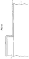
- FIG. 1 is a cross-sectional diagram of the completed phase-shifting mask according to the present invention.
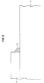
- FIG. 2 is a graph of phase-shift vs. normalized position along the phase-shifting spacer.
- FIGS. 3A-3E are cross-sectional diagrams of the process steps to fabricate the mask of the present invention.
- FIGS. 4A-4B are cross-sectional diagrams of a second embodiment of the invention.
- FIG. 5 is a cross-sectional diagram of a third embodiment of the invention.
- FIG. 6 is a cross-sectional diagram of a fourth embodiment of the invention.
- Referring to FIG. 1, a cross-sectional diagram of a section of the completed phase-shifting mask is shown.
Transparent layer 11 serves as a substrate for the patternedopaque layer 13 and self-aligned phase-shiftingspacers 15. Thetransparent layer 11 is chosen to transmit the wavelength of radiation used to expose a photoresist covered substrate (not shown), typically a semiconductor wafer. For visible and ultraviolet wavelengths, fused quartz is a preferredtransparent substrate 11 which is prevalently used in the industry. Fused silica is another substrate which is commonly used in optical mask design. The choice of substrate is based on the wavelength spectrum for which the substrate material must have excellent optical transmittance in the clear areas. The quartz substrate typically runs in the range of 4 to 10 mm (millimeters) in thickness. - The
opaque masking material 13 is chosen to absorb or reflect the exposing radiation, thus preventing exposure of the corresponding areas of the photoresist. Chrome is the industry standard for optical and ultraviolet masks. Chrome is used as an absorber based on its compatibility with the substrate, quartz, and the processes used for fabricating the mask, as well as other characteristics such as E-beam back scattering properties. Although chrome is a typical opaque absorber material, the invention is adaptable to other opaque materials. Preferably, the opaque material provides an etch stop for the blanket etch back of the phase-shifting material. A typical thickness of thechrome layer 13 is 0.1 µm (micro-meters), however, to accomodate the teachings of the invention it may be thicker depending on the respective refractive indices of thetransparent substrate 11 and thespacers 15. - In the preferred embodiment, the
spacers 15 are quarter-cylinders in cross-section and are approximately as thick and wide as the chrome layer is thick. A list of a few suitable materials for the phase-shifting spacers and their respective refractive indices are listed in Table I. While the table is not exhaustive, the desirable phase-shifting material should have excellent transmittance in the wavelength of the exposing radiation. Further, the phase-shifting material should optimally have an index of refraction of refraction in the region of 2.0 to 3.0 to avoid significantly increasing the thickness of the chrome layer from the 0.1 µm (micrometer) industry standard practice.TABLE I Material Index of Refraction (n) Transmittance g-line i-line Silicon Nitride (Si₃N₄) 2.10 2.04 > 90% Magnesium Fluoride (MgF₂) 1.39 1.38 > 90% Thorium Fluoride (ThF₄) 1.53 1.53 > 70% - To achieve a phase-shift of 180 degrees while maintaining the industry standard chrome thickness of 0.1 µm (micrometers) would require a material with an index of refraction of about 3.2, for g-line radiation according to the equation in the background.
- To achieve a phase-shift of 120 degrees while maintaining 0.1 µm (micrometers) thickness for g-line radiation would require a material with refractive index of about 2.5, referring to the same equation. That implies that all of the materials in Table 1 will require an increase in the chrome thickness.
- Typical wavelengths for the exposing radiation presently practiced are in the ultraviolet range of 0.436-0.365 µm (micrometers). In the future, it is expected that shorter wavelengths will be used. If silicon nitride were used as the material for the
spacers 15, thicknesses in the range of 0.12 to 0.2 µm (micrometers) would cause phase-shifts of 120 to 180 degrees for the ultraviolet range above. Thus, using silicon nitride, the chrome will be in same range, but possibly somewhat thicker than industry standards. - A series of calculations for g-line (0.436 µm (micron) wavelength) and i-line (0.365 µm (micron) wavelength) exposing radiation, for silicon nitride as the spacer material, with the following results are shown in Table II:


- From the above, the following can be concluded: a) for g-line with 120 degree phase-shifting, the required thickness increase over standard chrome is about 33%, while 180 degree phase-shifting the thickness is about doubled; b) for i-line and 120 degree phase-shifting, the increase over standard chrome is only 18% while 180 degree phase-shifting requires a 75% thickness increase; c) recognizing that the present and future trend of wavelength usage in the industry is toward i-line, an increase in chrome mask absorber material of 18-75% will be typically required.
- FIG. 2 depicts the phase-shift caused by the idealized phase-shifting spacer of FIG. 1 at various points along the spacer. The spacer is sufficiently thick at the chrome-spacer interface to create a 180 degree phase-shift and is a perfect quarter cylinder in cross-section. As can be seen, the phase-shift varies continuously from 180 degrees to zero degrees. The intensity distribution between light and dark areas is improved if the phase-shift varies gradually from 180 degrees to zero degrees. Thus, the present invention is a distinct improvement over the single-step phase-shifters of the prior art.
- The process steps to fabricate the phase-shifting mask of FIG. 1 are described with reference to FIGS. 3A-3E. In FIG. 3A, a layer of
opaque material 13 is shown deposited on thetransparent substrate 11. Evaporation is typically used for the chrome masking layer disposition followed by resist coating and patterning. The fabrication process for the underlying chrome-quartz mask is well known in the art. One of the objects of the invention is to produce a phase-shifting mask with processes which are as compatible with the conventional industry standards as possible. In the preferred embodiment, the thickness of theopaque layer 13 should equal the desired thickness of the spacer in the completed mask. Patternedphotoresist layer 17 is then formed, typically using conventional electron-beam lithography techniques. After the opaque material is etched, conventional inspection and repair procedures are carried out. The remaining resist 17 is stripped off resulting in the structure shown in FIG. 3B, a conventional optical photomask. - After the
opaque mask 13 is formed as shown in FIG. 3B, a conformal deposition of the phase-shiftingmaterial 15 is performed as shown in FIG. 3C. It is preferred that the coating be as conformal as possible to simplify spacer formation during etch with a minimum of substrate and opaque mask removal. Well known deposition techniques such as low pressure chemical vapor deposition (LPCVD), plasma enhanced chemical vapor deposition (PECVD), atmospheric pressure chemical vapor deposition (APCVD) or sputtering can be used for the deposition depending on the phase-shifting material. In the preferred embodiment, the phase-shifting material should be deposited at least as thick as the eventual spacer thickness. The silicon nitride deposition is typically a noncrystaline film prepared by high-temperature, low-pressure pyrolytic decomposition of a mixture of silane (SiH4) and ammonia (NH3), to achieve a conformal coating with nearly ideal stochiometry. The process may be plasma assisted as required. - Next, an anisotropic etch is performed in a RIE reactor represented by the arrows in FIG. 3D. As is well known in the art, an anisotropic etch etches predominantly in the vertical direction, having little to no horizontal undercut. It is preferred that the etch process be highly selective to the
spacer material 15, leaving thetransparent substrate 11 andopaque material 13 relatively unetched. The blanket etch process for silicon nitride typically would be carried out with carbon tetrafluoride (CF4) with 10% hydrogen (H2) at low pressure (less than 50 milliTorr) in a plasma etch tool operating in reactive ion etch (RIE) mode, to produce an anisotropic (vertical) etching result with minimum etch bias. The large expanses of thechrome 13 andquartz 11 relative to the spacer size as shown in FIG. 3E provide a very clear endpoint for the etch process. However, if the etch process was not highly selective to the phase-shiftingmaterial 15 versus thesubstrate 11, some overetch is easily tolerated as the substrate is very thick relative to the spacer material which is only a few hundred nanometers thick. As the thickness of the spacer material immediately adjacent to the edge of theopaque pattern 13 is greater than on the large expanse ofquartz 11 andchrome 13,spacers 15 remain at etch endpoint. - Other spacer shapes and sizes are encompassed by the present invention. By the nomenclature of the present description, all of these shapes are considered to be roughly quarter-cylindrical in cross-section. For example, in FIGS. 4A and 4B, a second embodiment of the invention is shown. In FIG. 4A, a thinner layer of the phase-shifting
material 15 is deposited over thechrome 13 andquartz 11. After etching the phase-shift material, thespacer 15 formed as shown in FIG. 4B is much thinner than it is tall. A thinner spacer may have advantages in tightly packed areas. Also, the variation in height, and therefore, in the phase-shift experienced by the exposing radiation is less over the width of the spacer. - In fact, with the proper choice of phase-shifting
material 15, the deposited thickness of the phase-shifting material and thickness of theopaque mask material 13, it is possible, albeit less preferred, to eliminate the etch step. As the coating of thespacer material 15 is conformal, the areas immediately adjacent to the opaque material have a height greater than in the field areas some distance from the opaque pattern. Although all the exposing radiation will be phase-shifted to some degree, it is possible to adjust the thicknesses of materials such that the exposing radiation which goes through the spacer areas is phase-shifted in the range of 0.67 pi to pi radians from the exposing radiation which passes through the thinner thickness of phase-shiftingmaterial 15 in the field areas. Due to attenuation in the field areas, however, it is preferred to perform the etch step to remove the excess phase-shiftingmaterial 15. - In FIG. 5, the effects of an overetch of the
spacer 15 shown in FIG. 3E is depicted. The spacer is thinner than theopaque mask 13, but still could be of the requisite thickness to accomplish the phase-shift. Rather than adjusting the chrome thickness as shown above in Table II, an over-etch is another way of tailoring the spacer height rather than changing the height for the desired phase-shift. - In FIG. 6, yet another embodiment of the invention is shown. A thin layer of phase-shifting material is left over the clear areas of the
transparent substrate 11 and theopaque masking areas 13 due to underetch. The phase-shiftingmaterial 15 over theopaque area 13 has no effect as the exposing radiation is absorbed or reflected in these areas. As discussed above, the phase-shift material in the transparent field areas is not desirable as it reduces the exposure energy to the resist. However, so long as the phase-shift due to the thick spacer area and the phase-shift due to the thin layer are 120 to 180 degrees out of phase, the current invention should work. - The phase-shifting masks of the present invention can be put to other uses besides semiconductor wafer fabrication. In X-ray lithography, a "mother" optical mask is used to fabricate a "daughter" X-ray mask. Through the use of the present invention, the resolution possible for X-ray lithography is also extended. The present invention is a simple means of converting a conventional optical mask into a self-aligned phase-shifting mask thus, improving the resolution possible with a minimum of extra cost.
Claims (10)
- A method for fabricating a self-aligned pase-shifting mask comprising the steps of:
providing a pattern of material (13) opaque to exposing radiation of a selected wavelength on selected areas of a horizontal surface of a substrate (11) which is transparent to the exposing radiation, the opaque pattern (13) having a horizontal surface and a vertical edge; and,
forming a spacer (15) of phase-shifting material on the vertical edge of the opaque pattern (13) by depositing phase-shifting material on the vertical edge and the horizontal surfaces of the opaque pattern (13) and the transparent substrate (11), the spacer (15) having a thickness at the vertical edge such that exposing radiation passing through the spacer (15) is phase-shifted in the range of 0.67 pi to pi radians with respect to exposing radiation passing through other areas of the mask. - A method of converting an optical lithography mask comprised of a patterned opaque material (13) on selected areas of a horizontal surface of a substrate (11) which is transparent to the exposing radiation, the opaque pattern (13) having a horizontal surface and a vertical edge into a self-aligned phase shifting mask comprising the step of:
forming a spacer (15) of phase-shifting material on the vertical edge of the opaque pattern (13) by depositing phase-shifting material on the vertical edge and the horizontal surfaces of the opaque pattern (13) and the transparent substrate (11), the spacer (15) having a thickness at the vertical edge such that exposing radiation passing through the spacer (15) is phase-shifted in the range of 0.67 pi to pi radians with respect to exposing radiation passing through other areas of the mask. - The method as recited in claim 1 or 2 wherein the forming step further comprises the step of etching the phase-shifting material to substantially remove it from the horizontal surfaces.
- The method as recited in one or more of the preceding claims 1 to 3 wherein the thickness of the spacer (15) at the vertical edge is substantially equal or similar to a thickness of the opaque pattern (13).
- The method as recited in one or more of the preceding claims 1 to 4 wherein a cross-sectional shape of the spacer (15) is a quarter-cylinder with its greatest thickness at the vertical edge of the opaque pattern (13) so that the greatest phase-shift of the exposing radiation is created at the edge or at the vertical edge of the opaque pattern (13).
- A self-aligned phase-shifting mask comprising:
a substrate (11) which is transparent to a selected wavelength of exposing radiation, having a horizontal surface;
a pattern of material (13) opaque to the selected wavelength of exposing radiation disposed on selected areas of the transparent substrate (11), the opaque pattern (13) having a vertical edge and a horizontal surface; and,
a self-aligned pattern of spacers (15) of phase-shifting material formed on the vertical edge of the opaque pattern (13) and the horizontal surface of the transparent substrate (11) of a thickness to cause a phase-shift in the exposing radiation passing through the spacers of 0.67 pi to pi radians with respect to the exposing radiation which passes through other areas of the mask. - The mask as recited in claim 6 wherein the thickness of the psacers (15) at the vertical edge is substantially similar to a thickness of the opaque pattern (13).
- The mask as recited in claim 6 or 7 wherein the phase-shifting material (15) is substantially removed from the horizontal surfaces of opaque pattern (13) and the transparent substrate (11).
- The mask as recited in one or more of the preceding claims 6 to 8 wherein a cross-sectional shape of the spacers (15) is a quarter-cylinder with a greatest thickness at the vertical edge of the opaque pattern (13) so that the greatest phase-shift of the exposing radiation is created at the vertical edge of the opaque pattern (13).
- The method or the mask as recited in one or more of the preceding claims 1 to 9 wherein the transparent substrate (11) is quartz and the opaque material (13) is chrome.
Applications Claiming Priority (2)
| Application Number | Priority Date | Filing Date | Title |
|---|---|---|---|
| US821385 | 1986-01-21 | ||
| US07/821,385 US5382483A (en) | 1992-01-13 | 1992-01-13 | Self-aligned phase-shifting mask |
Publications (1)
| Publication Number | Publication Date |
|---|---|
| EP0551621A1 true EP0551621A1 (en) | 1993-07-21 |
Family
ID=25233252
Family Applications (1)
| Application Number | Title | Priority Date | Filing Date |
|---|---|---|---|
| EP92121249A Withdrawn EP0551621A1 (en) | 1992-01-13 | 1992-12-14 | Self-aligned phase-shifting mask |
Country Status (5)
| Country | Link |
|---|---|
| US (1) | US5382483A (en) |
| EP (1) | EP0551621A1 (en) |
| JP (1) | JPH05265186A (en) |
| BR (1) | BR9205013A (en) |
| CA (1) | CA2082869A1 (en) |
Cited By (3)
| Publication number | Priority date | Publication date | Assignee | Title |
|---|---|---|---|---|
| EP0660185A2 (en) * | 1993-12-23 | 1995-06-28 | International Business Machines Corporation | Simplified fabrication methods for rim phase-shift masks |
| EP0666503A1 (en) * | 1994-02-07 | 1995-08-09 | Samsung Electronics Co., Ltd. | Photo mask and method for manufacturing the same |
| TWI423432B (en) * | 2008-09-12 | 2014-01-11 | Hon Hai Prec Ind Co Ltd | Spacer array and method for making same |
Families Citing this family (18)
| Publication number | Priority date | Publication date | Assignee | Title |
|---|---|---|---|---|
| KR0135149B1 (en) * | 1994-06-21 | 1998-04-25 | 문정환 | Fabrication method of phase shift mask |
| US5538833A (en) * | 1994-08-03 | 1996-07-23 | International Business Machines Corporation | High resolution phase edge lithography without the need for a trim mask |
| US5591549A (en) * | 1994-09-16 | 1997-01-07 | United Microelectronics Corporation | Self aligning fabrication method for sub-resolution phase shift mask |
| JP2972528B2 (en) * | 1994-10-14 | 1999-11-08 | 日本電気株式会社 | Exposure method |
| US5766829A (en) * | 1995-05-30 | 1998-06-16 | Micron Technology, Inc. | Method of phase shift lithography |
| US5582939A (en) * | 1995-07-10 | 1996-12-10 | Micron Technology, Inc. | Method for fabricating and using defect-free phase shifting masks |
| US6066555A (en) | 1995-12-22 | 2000-05-23 | Cypress Semiconductor Corporation | Method for eliminating lateral spacer erosion on enclosed contact topographies during RF sputter cleaning |
| US5955222A (en) * | 1996-12-03 | 1999-09-21 | International Business Machines Corporation | Method of making a rim-type phase-shift mask and mask manufactured thereby |
| US5792578A (en) * | 1997-01-13 | 1998-08-11 | Taiwan Semiconductor Manufacturing Company Ltd. | Method of forming multiple layer attenuating phase shifting masks |
| TW324074B (en) * | 1997-02-14 | 1998-01-01 | United Microelectronics Corp | Manufacturing method of phase shifting mask |
| KR100546269B1 (en) * | 1998-03-03 | 2006-04-21 | 삼성전자주식회사 | Half-tone phase shift mask and manufacturing method thereof |
| US6163367A (en) * | 1998-07-16 | 2000-12-19 | International Business Machines Corporation | Apparatus and method for in-situ adjustment of light transmission in a photolithography process |
| US6203941B1 (en) | 1998-12-18 | 2001-03-20 | Eveready Battery Company, Inc. | Formed in situ separator for a battery |
| KR20020017847A (en) * | 2000-08-31 | 2002-03-07 | 박종섭 | A method for forming a phase shift mask |
| US6716362B1 (en) | 2000-10-24 | 2004-04-06 | International Business Machines Corporation | Method for thin film laser reflectance correlation for substrate etch endpoint |
| AU2002236520A1 (en) | 2000-12-01 | 2002-06-11 | Unaxis Usa Inc. | Embedded attenuated phase shift mask and method of making embedded attenuated phase shift mask |
| JP2006292840A (en) * | 2005-04-06 | 2006-10-26 | Advanced Lcd Technologies Development Center Co Ltd | Exposure method and halftone phase shift mask |
| JP6714801B2 (en) * | 2016-03-31 | 2020-07-01 | インテル・コーポレーション | High resolution photomask or reticle and manufacturing method thereof |
Citations (5)
| Publication number | Priority date | Publication date | Assignee | Title |
|---|---|---|---|---|
| EP0437376A2 (en) * | 1990-01-12 | 1991-07-17 | Sony Corporation | Phase shifting masks and methods of manufacture |
| US5045417A (en) * | 1988-11-22 | 1991-09-03 | Hitachi, Ltd. | Mask for manufacturing semiconductor device and method of manufacture thereof |
| EP0453310A1 (en) * | 1990-04-19 | 1991-10-23 | Sharp Kabushiki Kaisha | Mask for photolithography |
| EP0489540A2 (en) * | 1990-12-05 | 1992-06-10 | AT&T Corp. | Phase-shifting lithographic masks with improved resolution |
| DE4215210A1 (en) * | 1991-05-09 | 1992-11-12 | Gold Star Electronics | Optical phase shifting mask mfr. - has sidewall phase shifting layer on both sides of each phase shifting layer for spatial frequency modulation |
Family Cites Families (11)
| Publication number | Priority date | Publication date | Assignee | Title |
|---|---|---|---|---|
| FR1548401A (en) * | 1967-08-16 | 1968-12-06 | ||
| US3742229A (en) * | 1972-06-29 | 1973-06-26 | Massachusetts Inst Technology | Soft x-ray mask alignment system |
| GB2066487B (en) * | 1979-12-18 | 1983-11-23 | Philips Electronic Associated | Alignment of exposure masks |
| US4707218A (en) * | 1986-10-28 | 1987-11-17 | International Business Machines Corporation | Lithographic image size reduction |
| US4885231A (en) * | 1988-05-06 | 1989-12-05 | Bell Communications Research, Inc. | Phase-shifted gratings by selective image reversal of photoresist |
| JP2735589B2 (en) * | 1988-12-06 | 1998-04-02 | 富士通株式会社 | Manufacturing method of diffraction grating |
| JPH02211450A (en) * | 1989-02-10 | 1990-08-22 | Fujitsu Ltd | Phase shift mask and its manufacture |
| JPH02247647A (en) * | 1989-03-20 | 1990-10-03 | Fujitsu Ltd | Production of phase shift mask |
| JPH02287542A (en) * | 1989-04-28 | 1990-11-27 | Fujitsu Ltd | Phase shift mask |
| JPH0440455A (en) * | 1990-06-06 | 1992-02-10 | Sony Corp | Manufacture of phase shift mask |
| JP2965655B2 (en) * | 1990-10-08 | 1999-10-18 | 松下電器産業株式会社 | Pattern formation method |
-
1992
- 1992-01-13 US US07/821,385 patent/US5382483A/en not_active Expired - Fee Related
- 1992-11-13 CA CA002082869A patent/CA2082869A1/en not_active Abandoned
- 1992-12-14 EP EP92121249A patent/EP0551621A1/en not_active Withdrawn
- 1992-12-15 BR BR9205013A patent/BR9205013A/en not_active IP Right Cessation
- 1992-12-24 JP JP34443992A patent/JPH05265186A/en active Pending
Patent Citations (5)
| Publication number | Priority date | Publication date | Assignee | Title |
|---|---|---|---|---|
| US5045417A (en) * | 1988-11-22 | 1991-09-03 | Hitachi, Ltd. | Mask for manufacturing semiconductor device and method of manufacture thereof |
| EP0437376A2 (en) * | 1990-01-12 | 1991-07-17 | Sony Corporation | Phase shifting masks and methods of manufacture |
| EP0453310A1 (en) * | 1990-04-19 | 1991-10-23 | Sharp Kabushiki Kaisha | Mask for photolithography |
| EP0489540A2 (en) * | 1990-12-05 | 1992-06-10 | AT&T Corp. | Phase-shifting lithographic masks with improved resolution |
| DE4215210A1 (en) * | 1991-05-09 | 1992-11-12 | Gold Star Electronics | Optical phase shifting mask mfr. - has sidewall phase shifting layer on both sides of each phase shifting layer for spatial frequency modulation |
Non-Patent Citations (2)
| Title |
|---|
| PATENT ABSTRACTS OF JAPAN vol. 16, no. 216 (P-1356)21 May 1992 & JP-A-04 040455 ( SONY CORP ) 10 February 1992 * |
| PATENT ABSTRACTS OF JAPAN vol. 16, no. 423 (E-1260)7 September 1992 & JP-A-04 146617 ( MATSUSHITA ELECTRIC IND CO LTD ) 20 May 1992 * |
Cited By (4)
| Publication number | Priority date | Publication date | Assignee | Title |
|---|---|---|---|---|
| EP0660185A2 (en) * | 1993-12-23 | 1995-06-28 | International Business Machines Corporation | Simplified fabrication methods for rim phase-shift masks |
| EP0660185A3 (en) * | 1993-12-23 | 1996-07-17 | Ibm | Simplified fabrication methods for rim phase-shift masks. |
| EP0666503A1 (en) * | 1994-02-07 | 1995-08-09 | Samsung Electronics Co., Ltd. | Photo mask and method for manufacturing the same |
| TWI423432B (en) * | 2008-09-12 | 2014-01-11 | Hon Hai Prec Ind Co Ltd | Spacer array and method for making same |
Also Published As
| Publication number | Publication date |
|---|---|
| JPH05265186A (en) | 1993-10-15 |
| CA2082869A1 (en) | 1993-07-14 |
| US5382483A (en) | 1995-01-17 |
| BR9205013A (en) | 1993-09-14 |
Similar Documents
| Publication | Publication Date | Title |
|---|---|---|
| US5382483A (en) | Self-aligned phase-shifting mask | |
| US7226708B2 (en) | Multi-layer, attenuated phase-shifting mask | |
| US5881125A (en) | Attenuated phase-shifted reticle using sub-resolution pattern | |
| EP0674223B1 (en) | An attenuating phase-shift mask structure and fabrication method | |
| US5358808A (en) | Exposure mask, method of manufacturing the same, and exposure method using the same | |
| US5286581A (en) | Phase-shift mask and method for making | |
| KR940007788B1 (en) | Mask for photolithography | |
| US5437947A (en) | Phase shifting mask and method of manufacturing the same | |
| EP0475694B1 (en) | Optical mask using phase shift and method of producing the same | |
| KR0170465B1 (en) | Photomask | |
| US5695896A (en) | Process for fabricating a phase shifting mask | |
| US5268244A (en) | Self-aligned phase shifter formation | |
| KR100399444B1 (en) | Edge reinforced phase reversal mask and its manufacturing method | |
| US6183915B1 (en) | Method of forming a phase shifting reticle | |
| US5591549A (en) | Self aligning fabrication method for sub-resolution phase shift mask | |
| US5744268A (en) | Phase shift mask, method of manufacturing a phase shift mask and method of forming a pattern with phase shift mask | |
| US5294506A (en) | Photomask | |
| US6348288B1 (en) | Resolution enhancement method for deep quarter micron technology | |
| CN115981094B (en) | Photomask, method for manufacturing photomask, and pattern forming method using photomask | |
| KR940008360B1 (en) | Manufacturing method of lens type mask | |
| KR0146243B1 (en) | Exposure mask and the manufacturing method thereof | |
| JPH05281702A (en) | Production of phase shift mask | |
| KR20020063960A (en) | Method for manufacturing mask | |
| KR20010019170A (en) | Method for fabricating photomask and structure thereof | |
| JPH05313349A (en) | Reticule for stepper |
Legal Events
| Date | Code | Title | Description |
|---|---|---|---|
| PUAI | Public reference made under article 153(3) epc to a published international application that has entered the european phase |
Free format text: ORIGINAL CODE: 0009012 |
|
| AK | Designated contracting states |
Kind code of ref document: A1 Designated state(s): BE CH DE ES FR GB IT LI NL SE |
|
| 17P | Request for examination filed |
Effective date: 19931119 |
|
| 17Q | First examination report despatched |
Effective date: 19961223 |
|
| STAA | Information on the status of an ep patent application or granted ep patent |
Free format text: STATUS: THE APPLICATION IS DEEMED TO BE WITHDRAWN |
|
| 18D | Application deemed to be withdrawn |
Effective date: 19970503 |