EP0560550B1 - Shielded back plane connector - Google Patents
Shielded back plane connector Download PDFInfo
- Publication number
- EP0560550B1 EP0560550B1 EP93301725A EP93301725A EP0560550B1 EP 0560550 B1 EP0560550 B1 EP 0560550B1 EP 93301725 A EP93301725 A EP 93301725A EP 93301725 A EP93301725 A EP 93301725A EP 0560550 B1 EP0560550 B1 EP 0560550B1
- Authority
- EP
- European Patent Office
- Prior art keywords
- shield
- electrical connector
- connector
- web
- contact
- Prior art date
- Legal status (The legal status is an assumption and is not a legal conclusion. Google has not performed a legal analysis and makes no representation as to the accuracy of the status listed.)
- Expired - Lifetime
Links
Images
Classifications
-
- H—ELECTRICITY
- H01—ELECTRIC ELEMENTS
- H01R—ELECTRICALLY-CONDUCTIVE CONNECTIONS; STRUCTURAL ASSOCIATIONS OF A PLURALITY OF MUTUALLY-INSULATED ELECTRICAL CONNECTING ELEMENTS; COUPLING DEVICES; CURRENT COLLECTORS
- H01R13/00—Details of coupling devices of the kinds covered by groups H01R12/70 or H01R24/00 - H01R33/00
- H01R13/648—Protective earth or shield arrangements on coupling devices, e.g. anti-static shielding
- H01R13/658—High frequency shielding arrangements, e.g. against EMI [Electro-Magnetic Interference] or EMP [Electro-Magnetic Pulse]
- H01R13/6581—Shield structure
- H01R13/6585—Shielding material individually surrounding or interposed between mutually spaced contacts
- H01R13/6586—Shielding material individually surrounding or interposed between mutually spaced contacts for separating multiple connector modules
- H01R13/6587—Shielding material individually surrounding or interposed between mutually spaced contacts for separating multiple connector modules for mounting on PCBs
-
- H—ELECTRICITY
- H01—ELECTRIC ELEMENTS
- H01R—ELECTRICALLY-CONDUCTIVE CONNECTIONS; STRUCTURAL ASSOCIATIONS OF A PLURALITY OF MUTUALLY-INSULATED ELECTRICAL CONNECTING ELEMENTS; COUPLING DEVICES; CURRENT COLLECTORS
- H01R12/00—Structural associations of a plurality of mutually-insulated electrical connecting elements, specially adapted for printed circuits, e.g. printed circuit boards [PCB], flat or ribbon cables, or like generally planar structures, e.g. terminal strips, terminal blocks; Coupling devices specially adapted for printed circuits, flat or ribbon cables, or like generally planar structures; Terminals specially adapted for contact with, or insertion into, printed circuits, flat or ribbon cables, or like generally planar structures
- H01R12/70—Coupling devices
- H01R12/71—Coupling devices for rigid printing circuits or like structures
- H01R12/72—Coupling devices for rigid printing circuits or like structures coupling with the edge of the rigid printed circuits or like structures
- H01R12/722—Coupling devices for rigid printing circuits or like structures coupling with the edge of the rigid printed circuits or like structures coupling devices mounted on the edge of the printed circuits
- H01R12/724—Coupling devices for rigid printing circuits or like structures coupling with the edge of the rigid printed circuits or like structures coupling devices mounted on the edge of the printed circuits containing contact members forming a right angle
-
- H—ELECTRICITY
- H01—ELECTRIC ELEMENTS
- H01R—ELECTRICALLY-CONDUCTIVE CONNECTIONS; STRUCTURAL ASSOCIATIONS OF A PLURALITY OF MUTUALLY-INSULATED ELECTRICAL CONNECTING ELEMENTS; COUPLING DEVICES; CURRENT COLLECTORS
- H01R12/00—Structural associations of a plurality of mutually-insulated electrical connecting elements, specially adapted for printed circuits, e.g. printed circuit boards [PCB], flat or ribbon cables, or like generally planar structures, e.g. terminal strips, terminal blocks; Coupling devices specially adapted for printed circuits, flat or ribbon cables, or like generally planar structures; Terminals specially adapted for contact with, or insertion into, printed circuits, flat or ribbon cables, or like generally planar structures
- H01R12/70—Coupling devices
- H01R12/71—Coupling devices for rigid printing circuits or like structures
- H01R12/72—Coupling devices for rigid printing circuits or like structures coupling with the edge of the rigid printed circuits or like structures
- H01R12/722—Coupling devices for rigid printing circuits or like structures coupling with the edge of the rigid printed circuits or like structures coupling devices mounted on the edge of the printed circuits
- H01R12/727—Coupling devices presenting arrays of contacts
-
- H—ELECTRICITY
- H01—ELECTRIC ELEMENTS
- H01R—ELECTRICALLY-CONDUCTIVE CONNECTIONS; STRUCTURAL ASSOCIATIONS OF A PLURALITY OF MUTUALLY-INSULATED ELECTRICAL CONNECTING ELEMENTS; COUPLING DEVICES; CURRENT COLLECTORS
- H01R31/00—Coupling parts supported only by co-operation with counterpart
Definitions
- the present invention relates to a shielded back plane connector which can be mounted to a back plane, which receives a shielded daughter card connector.
- a header connector having a plurality of male pins is mounted to a mother board connector.
- a daughter board connector is mounted to a daughter card and is profiled for receipt within the header connector, the daughter board connector having a plurality of receptacle sockets for electrical connection with the male pins in the header.
- a further object of the invention is to provide for a shielded back plane assembly having overall reduced dimensions, without compromising on other characteristics such as EMI/RFI, signal speed, and the like.
- a further object of the invention is to substantially eliminate the cross-talk between adjacent terminals.
- a high density shielded back plane connector comprising a front housing portion and a plurality of terminal sub assemblies fixed to the front housing, the terminal sub assemblies comprising front mating contact portions positioned in the front housing portion, an intermediate portion moulded in an insulative web of material and a rear contact portion extending from the web of material and adapted for mating with further conductors.
- a shield portion is positioned intermediate each of the plastic webs where the web includes a reduced thickness of a reduced thickness section in the web on both sides thereof the reduced thickness portion forms a thin membrane over a substantial portion of the intermediate portions thereby increasing the impedance along the intermediate portions interiorly of the shields.
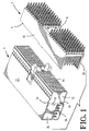
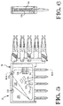
- FIG. 1 is an isometric view of a header connector shown generally at 2 and a shielded daughter card connector shown generally at 4.
- the header assembly 2 is generally comprised of an insulating housing 6 having a lower surface 8 for mounting to a mother board and side walls 10 upstanding from the floor portion 8.
- the daughter board connector 4 is generally comprised of a forward housing portion 12 having a front mating face 14 side surfaces 16 and a rear surface 18.
- a plurality of terminal sub-assemblies 20 are shown assembled to the housing 12 and encapsulated in upper and lower shield members 22, 24 respectively.
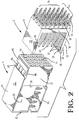
- the header housing 6 has side walls 10 comprised of thin side wall sections 26 having end strengthening ribs 28 and 30. Along the interior length of the thin side wall section 26, a plurality of strengthening ribs 32 are positioned integral with the sidewall 10 to rigidify these thin side wall sections.
- the header assembly 2 further comprises a plurality of signal contacts 36 having compliant pin portions 38 extending outwardly from the floor 8 and further include male pin portions 40 positioned within the header intermediate the side walls 10.
- the header assembly 2 further comprises a plurality of grounding contacts 44 having compliant pin portions 46 and a grounding pin portion 48 positioned between strengthening ribs 32.
- Housing 12 includes a plurality of signal pin contact receiving openings shown at 50 leading into a terminal receiving passageway 52, the passageway 52 extending rearwardly to a face 54.
- a plurality of terminal subassemblies 20 are positioned against the housing 12 where each subassembly includes a plurality of electrical terminals 56 encapsulated in an overmoulded web of plastic material 58.
- Each contact 56 includes a receptacle portion 60 for mating contact with one of the male signal pins 40 and further comprises an intermediate portion 62, which interconnects the receptacle portions to and compliant pin portions 64.
- the upper shield member 22 includes an upper plate portion 70 for positioning above the housing portion 12 and above the terminal subassemblies 20.
- the upper shield member 22 further includes a rear plate portion 72 for positioning behind the terminal subassemblies 20, the rear plate portion 72 including a plurality of integral compliant pin sections 74 for mechanical and electrical connection to a printed circuit board 75, as shown in Figure 3.
- the upper shield member 22 further includes a thin plate portion 78 ( Figure 3) formed by a premilling operation to reduce the thickness of the shield portion over the housing 20 to reduce the overall width dimension of the shielded data board connection.
- the upper shield 22 is kinked adjacent to the front mating face 14 to form projections 82 extending above the plane formed by the upper plate portion 70.
- a plurality of windows 84 are stamped from the upper plate portion 70 whereby the windows are laterally positioned to receive the strengthening ribs 32 therein, while the projections 82 form shield contacts, which span the strengthening ribs 32, for mating with the ground pins 48.
- a strengthening strap 85 extends transversely of the shields contacts 82 and is held to the housing by a folded front edge 86 positioned in a laterally extending groove 88 ( Figure 3).
- a laterally extending channel 90 is positioned below the shield contacts 82.
- the lower shield member 24 is similar to the upper shield portion including a plate portion 95 having a thin wall section 96, shield contacts at 98, and compliant portions 99 for interconnection to the printed circuit board.
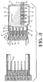
- the above mentioned daughter board connector 4 can alternatively be used with an additional shield placed intermediate the plurality of terminal sub-assemblies 20 to reduce the cross talk between the adjacent terminal strips.
- a cross talk shield 100 can be positioned between each adjacent stacked terminal sub-assembly 20.
- the cross talk shield 100 contacts the center terminal 56C leaving terminals 56A, 56B and 56D, 56E for signal contacts thereby forming a modified strip line connector.
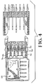
- the shielded sub-assembly 20 will be described in greater detail for use with the cross talk shield.
- the terminal sub-assembly 20 has an overmoulded web of material 58 having a recessed pocket at 102 and a recessed surface 104.
- a window is formed at 106 exposing a portion of the central terminal 56C for contacting with the cross talk shield 100.
- two apertures are formed through the insulating web 58 at 110 and a lower slot 112 is formed by two upstanding ribs 114 having a thickness equal to the raised portion 104 with the intermediate portion between the slot being recessed to the surface 102.
- the cross talk shield 100 has a flat plate portion 120 including two lower contact arms 122 for contact with a trace on a printed circuit board, and further comprises an upper contact arm shown at 124.
- the cross talk shield 100 further comprises locking tabs 126 at an upper edge thereof, and locking tab 128 at a lower edge thereof.
- the cross talk shield is formed with the contact arm 124 bent around an upper edge of the flat plate portion 122, and the end of the contact arm 124 is formed with a radius section thereby forming a contact surface 127 for contacting the central contact 56C.
- Figure 10 also shows cross-talk shield positioned on the surface 104, with the cooperation between the tabs 126 within the openings 110, and shows the tab 128 frictionally held between the two upstanding ribs 114 in the slot thereof.
- a plurality of cross talk shields 100 can be placed against the terminal sub-assemblies 20 to reduce the cross talk between adjacent terminal sub-assemblies.
- the cross-talk shields can be added without increasing the stack thickness of the terminal sub-assemblies and the shields 100, as the shields are positioned against the recessed surface 104.
- the impedance has been increased by the formation of the recessed surface 102, thereby providing a pocket of air adjacent to the terminals.
- the ground signal path has been reduced by providing two contact arms 122 adjacent to the daughter board and by providing the contact to the centre terminal 56C.
- the modules 20 can be stacked one against the other with the shield member therebetween. Due to the recessed area 104, which is profiled to receive the shield 100, the stacking thickness of the modules 20, remains the same, with or without the shields 100 therebetween.
- the connector system described above can be used without the cross talk shields 100, without having to change the contact modules 20.
Description
- The present invention relates to a shielded back plane connector which can be mounted to a back plane, which receives a shielded daughter card connector.
- It is common in electronic architecture to provide for a header connector having a plurality of male pins to be mounted to a mother board connector. A daughter board connector is mounted to a daughter card and is profiled for receipt within the header connector, the daughter board connector having a plurality of receptacle sockets for electrical connection with the male pins in the header.
- It is known to provide a shield between the vertical rows of terminals to prevent cross-talk between the vertical columns. For example, as shown in German patent application, DE-A-40 40 551, a cross-talk shield is placed intermediate the terminal subassemblies which form the connector. One of the drawbacks to the above-mentioned design is that a different terminal subassembly is necessary due to the thickness of the shield itself.
- It is an object of the invention then to provide a backplane connector having a cross-talk shield.
- A further object of the invention is to provide for a shielded back plane assembly having overall reduced dimensions, without compromising on other characteristics such as EMI/RFI, signal speed, and the like.
- A further object of the invention is to substantially eliminate the cross-talk between adjacent terminals.
- The objects were accomplished by providing an electrical connector as defined in claim 1. There is disclosed herein a high density shielded back plane connector comprising a front housing portion and a plurality of terminal sub assemblies fixed to the front housing, the terminal sub assemblies comprising front mating contact portions positioned in the front housing portion, an intermediate portion moulded in an insulative web of material and a rear contact portion extending from the web of material and adapted for mating with further conductors. A shield portion is positioned intermediate each of the plastic webs where the web includes a reduced thickness of a reduced thickness section in the web on both sides thereof the reduced thickness portion forms a thin membrane over a substantial portion of the intermediate portions thereby increasing the impedance along the intermediate portions interiorly of the shields.
- Embodiments of the present invention will now be described by way of example with reference to the accompanying drawings in which:
- Figure 1 is an isometric view of the shielded daughter board connector exploded from the complementary header;
- Figure 2 is an isometric view of an enlarged section of the connectors shown in Figure 1;
- Figure 3 is a cross-sectional view through the connector of Figure 1 or 2 showing the internal structure thereof;
- Figure 4 is a cross-sectional view similar to that of Figure 3 showing an alternative embodiment having a cross talk shield;
- Figure 5 is a side plan view of the terminal sub-assembly for use in the embodiment of Figure 4;
- Figure 6 is a cross-sectional view through lines 6-6 of Figure 5;
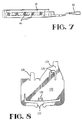
- Figure 7 is a lower plan view of the terminal sub-assembly shown in Figure 5;
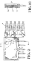
- Figure 8 is a plan view of the cross talk shield in a stamped blank form;
- Figure 9 is a side plan view showing the cross talk shield in place on the terminal sub-assembly;
- Figure 10 shows a cross-sectional view of the terminal sub-assembly through lines 10-10; and
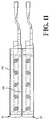
- Figure 11 shows a lower plan view of two of the sub-assemblies stacked together with the cross talk shield in place.
- Figure 1 is an isometric view of a header connector shown generally at 2 and a shielded daughter card connector shown generally at 4. The
header assembly 2 is generally comprised of aninsulating housing 6 having alower surface 8 for mounting to a mother board andside walls 10 upstanding from thefloor portion 8. With reference still to Figure 1, thedaughter board connector 4 is generally comprised of aforward housing portion 12 having afront mating face 14side surfaces 16 and arear surface 18. A plurality ofterminal sub-assemblies 20 are shown assembled to thehousing 12 and encapsulated in upper andlower shield members - With reference now to Figure 2, the
header assembly 2 and daughter board assembly will be described in greater detail, where Figure 2 is an enlarged section of the assemblies shown in Figure 1. As shown in Figure 2, theheader housing 6 hasside walls 10 comprised of thinside wall sections 26 havingend strengthening ribs side wall section 26, a plurality of strengtheningribs 32 are positioned integral with thesidewall 10 to rigidify these thin side wall sections. Theheader assembly 2 further comprises a plurality ofsignal contacts 36 havingcompliant pin portions 38 extending outwardly from thefloor 8 and further includemale pin portions 40 positioned within the header intermediate theside walls 10. Theheader assembly 2 further comprises a plurality ofgrounding contacts 44 havingcompliant pin portions 46 and agrounding pin portion 48 positioned between strengtheningribs 32. - With reference now to Figures 2 and 3, the
daughter board connector 4 will be described in greater detail.Housing 12 includes a plurality of signal pin contact receiving openings shown at 50 leading into aterminal receiving passageway 52, thepassageway 52 extending rearwardly to aface 54. A plurality ofterminal subassemblies 20 are positioned against thehousing 12 where each subassembly includes a plurality ofelectrical terminals 56 encapsulated in an overmoulded web ofplastic material 58. Eachcontact 56 includes areceptacle portion 60 for mating contact with one of themale signal pins 40 and further comprises anintermediate portion 62, which interconnects the receptacle portions to andcompliant pin portions 64. - With reference again to Figure 2, the
upper shield member 22 includes anupper plate portion 70 for positioning above thehousing portion 12 and above theterminal subassemblies 20. Theupper shield member 22 further includes arear plate portion 72 for positioning behind theterminal subassemblies 20, therear plate portion 72 including a plurality of integralcompliant pin sections 74 for mechanical and electrical connection to a printedcircuit board 75, as shown in Figure 3. Theupper shield member 22 further includes a thin plate portion 78 (Figure 3) formed by a premilling operation to reduce the thickness of the shield portion over thehousing 20 to reduce the overall width dimension of the shielded data board connection. As shown in Figure 2, theupper shield 22 is kinked adjacent to thefront mating face 14 to formprojections 82 extending above the plane formed by theupper plate portion 70. A plurality ofwindows 84 are stamped from theupper plate portion 70 whereby the windows are laterally positioned to receive the strengtheningribs 32 therein, while theprojections 82 form shield contacts, which span the strengtheningribs 32, for mating with theground pins 48. To rigidify the plurality of shield contacts 82 a strengtheningstrap 85 extends transversely of theshields contacts 82 and is held to the housing by a foldedfront edge 86 positioned in a laterally extending groove 88 (Figure 3). To improve the resiliency of the shield contacts 82 a laterally extendingchannel 90 is positioned below theshield contacts 82. Thelower shield member 24 is similar to the upper shield portion including aplate portion 95 having athin wall section 96, shield contacts at 98, andcompliant portions 99 for interconnection to the printed circuit board. - With reference now to Figure 4, the above mentioned
daughter board connector 4 can alternatively be used with an additional shield placed intermediate the plurality ofterminal sub-assemblies 20 to reduce the cross talk between the adjacent terminal strips. For this purpose, across talk shield 100 can be positioned between each adjacent stackedterminal sub-assembly 20. In the preferred embodiment of the invention thecross talk shield 100 contacts the center terminal 56C leaving terminals 56A, 56B and 56D, 56E for signal contacts thereby forming a modified strip line connector. - With reference now to Figure 5, the shielded
sub-assembly 20 will be described in greater detail for use with the cross talk shield. As mentioned above, theterminal sub-assembly 20 has an overmoulded web ofmaterial 58 having a recessed pocket at 102 and arecessed surface 104. As shown in Figures 5 and 6, a window is formed at 106 exposing a portion of the central terminal 56C for contacting with thecross talk shield 100. With reference again to Figure 5, two apertures are formed through theinsulating web 58 at 110 and alower slot 112 is formed by twoupstanding ribs 114 having a thickness equal to the raisedportion 104 with the intermediate portion between the slot being recessed to thesurface 102. With reference now to Figure 8, thecross talk shield 100 has aflat plate portion 120 including twolower contact arms 122 for contact with a trace on a printed circuit board, and further comprises an upper contact arm shown at 124. Thecross talk shield 100 further compriseslocking tabs 126 at an upper edge thereof, and lockingtab 128 at a lower edge thereof. As shown in Figure 10, the cross talk shield is formed with thecontact arm 124 bent around an upper edge of theflat plate portion 122, and the end of thecontact arm 124 is formed with a radius section thereby forming acontact surface 127 for contacting the central contact 56C. Figure 10 also shows cross-talk shield positioned on thesurface 104, with the cooperation between thetabs 126 within theopenings 110, and shows thetab 128 frictionally held between the twoupstanding ribs 114 in the slot thereof. As shown in Figures 10 and 11, a plurality ofcross talk shields 100 can be placed against theterminal sub-assemblies 20 to reduce the cross talk between adjacent terminal sub-assemblies. The cross-talk shields can be added without increasing the stack thickness of the terminal sub-assemblies and theshields 100, as the shields are positioned against therecessed surface 104. - Advantageously then, as the center line distance between adjacent terminals in
adjacent terminal sub-assemblies 20 has been reduced by half, by the addition of thecross talk shield 100, the impedance has been increased by the formation of therecessed surface 102, thereby providing a pocket of air adjacent to the terminals. Furthermore the ground signal path has been reduced by providing twocontact arms 122 adjacent to the daughter board and by providing the contact to the centre terminal 56C. Moreover, as shown in Figure 11, themodules 20 can be stacked one against the other with the shield member therebetween. Due to therecessed area 104, which is profiled to receive theshield 100, the stacking thickness of themodules 20, remains the same, with or without theshields 100 therebetween. Thus, the connector system described above can be used without thecross talk shields 100, without having to change thecontact modules 20.
Claims (10)
- An electrical connector (4) having a front housing portion (12) and a plurality of side by side terminal subassemblies (20) fixed to said front housing portion (12), the terminal subassemblies (20) comprising a front mating contact portion (60) positioned in said front housing portion (12), an intermediate portion (62) moulded in an insulative web (58) of material, and a rear contact portion (64) extending from said web of material (58) and adapted for mating with further conductors, and a shield portion (100) positioned intermediate each pair of adjacent webs (38), said connector (4) being characterized in that each web (58) includes a pocket (102) on both sides of said intermediate portions (62), said pocket (102) forming a thin membrane of said insulative material over a substantial portion of said intermediate portions (62) with the shield portion (100) positioned, thereby forming a pocket of air between said intermediate portions (62) and said shield portion (100), thereby increasing the impedance along the intermediate portions (62), interiorly of said shield portions (100).
- An electrical connector (4) according to claim 1, characterized in that, said web (58) includes a window (106) therethrough exposing one of said intermediate portions (62) of one select terminal (56c), and said shield portion (100) includes a resilient contact portion (126) for contacting said selected intermediate portion (62).
- An electrical connector (4) according to claim 1, characterized in that said resilient contact portion (126) is formed from a reversely bent contact leg (124) which extends integrally from said shield portion (100).
- An electrical connector (4) according to claims 2 or 3, characterized in that the resilient contact portion (126) is formed by a portion extending from one edge thereof.
- An electrical connector (4) according to any one of claims 1 to 4, characterized in that said connector includes five electrical terminals (56) positioned in said subassemblies (20).
- An electrical connector (4) according to any one of claims 1 to 5, characterized in that said terminals (56) are arranged in two pairs of signal contacts with the intermediate contact (56c) being said selected one, to ground said shield portion (100).
- An electrical connector (4) according to any one of claims 1 to 6, characterized in that said connector (4) is profiled as a right angled connector where said rear mating contact portions (64) extend from said web (58) at a substantial right angle relative to said front mating contact portions (60), said webs (58) including a lower edge profiled for receiving a printed circuit board thereagainst.
- An electrical connector (4) according to claim 7, characterized in that said shield portion (100) includes a second resilient contact portion (122) extending below said web lower edge, for contacting a ground plate on said printed circuit board.
- An electrical connector (4) according to any one of claims 1 to 8, characterized in that said shield portion (100) includes two resilient contact arms (122) extending from a lower edge thereof, profiled to contact a grounding pad on a printed circuit board.
- An electrical connector (4) according to any one of claims 1 to 9, characterized in that said web (58) includes a recess (104)about each pocket (102), profiled for receiving the shield portion (100) thereagainst, such that the stacking thickness of the subassemblies (20) remains constant whether the shield portion (100) is present or not.
Priority Applications (1)
| Application Number | Priority Date | Filing Date | Title |
|---|---|---|---|
| EP96201938A EP0746060B1 (en) | 1992-03-09 | 1993-03-08 | Shielded back plane connector |
Applications Claiming Priority (2)
| Application Number | Priority Date | Filing Date | Title |
|---|---|---|---|
| GB929205088A GB9205088D0 (en) | 1992-03-09 | 1992-03-09 | Shielded back plane connector |
| GB9205088 | 1992-03-09 |
Related Child Applications (2)
| Application Number | Title | Priority Date | Filing Date |
|---|---|---|---|
| EP96201938A Division EP0746060B1 (en) | 1992-03-09 | 1993-03-08 | Shielded back plane connector |
| EP96201938.6 Division-Into | 1996-07-10 |
Publications (3)
| Publication Number | Publication Date |
|---|---|
| EP0560550A2 EP0560550A2 (en) | 1993-09-15 |
| EP0560550A3 EP0560550A3 (en) | 1994-03-09 |
| EP0560550B1 true EP0560550B1 (en) | 1997-07-16 |
Family
ID=10711764
Family Applications (2)
| Application Number | Title | Priority Date | Filing Date |
|---|---|---|---|
| EP96201938A Expired - Lifetime EP0746060B1 (en) | 1992-03-09 | 1993-03-08 | Shielded back plane connector |
| EP93301725A Expired - Lifetime EP0560550B1 (en) | 1992-03-09 | 1993-03-08 | Shielded back plane connector |
Family Applications Before (1)
| Application Number | Title | Priority Date | Filing Date |
|---|---|---|---|
| EP96201938A Expired - Lifetime EP0746060B1 (en) | 1992-03-09 | 1993-03-08 | Shielded back plane connector |
Country Status (6)
| Country | Link |
|---|---|
| US (1) | US5342211A (en) |
| EP (2) | EP0746060B1 (en) |
| JP (1) | JP3410501B2 (en) |
| DE (2) | DE69327881T2 (en) |
| ES (1) | ES2104052T3 (en) |
| GB (1) | GB9205088D0 (en) |
Cited By (13)
| Publication number | Priority date | Publication date | Assignee | Title |
|---|---|---|---|---|
| DE19938782A1 (en) * | 1999-08-16 | 2001-03-22 | Tyco Electronics Logistics Ag | Shielded electrical connector |
| US8231415B2 (en) | 2009-07-10 | 2012-07-31 | Fci Americas Technology Llc | High speed backplane connector with impedance modification and skew correction |
| US8366485B2 (en) | 2009-03-19 | 2013-02-05 | Fci Americas Technology Llc | Electrical connector having ribbed ground plate |
| USD718253S1 (en) | 2012-04-13 | 2014-11-25 | Fci Americas Technology Llc | Electrical cable connector |
| US8905651B2 (en) | 2012-01-31 | 2014-12-09 | Fci | Dismountable optical coupling device |
| USD720698S1 (en) | 2013-03-15 | 2015-01-06 | Fci Americas Technology Llc | Electrical cable connector |
| US8944831B2 (en) | 2012-04-13 | 2015-02-03 | Fci Americas Technology Llc | Electrical connector having ribbed ground plate with engagement members |
| USD727268S1 (en) | 2012-04-13 | 2015-04-21 | Fci Americas Technology Llc | Vertical electrical connector |
| USD727852S1 (en) | 2012-04-13 | 2015-04-28 | Fci Americas Technology Llc | Ground shield for a right angle electrical connector |
| USD733662S1 (en) | 2013-01-25 | 2015-07-07 | Fci Americas Technology Llc | Connector housing for electrical connector |
| USD746236S1 (en) | 2012-07-11 | 2015-12-29 | Fci Americas Technology Llc | Electrical connector housing |
| US9257778B2 (en) | 2012-04-13 | 2016-02-09 | Fci Americas Technology | High speed electrical connector |
| US9543703B2 (en) | 2012-07-11 | 2017-01-10 | Fci Americas Technology Llc | Electrical connector with reduced stack height |
Families Citing this family (119)
| Publication number | Priority date | Publication date | Assignee | Title |
|---|---|---|---|---|
| GB9307127D0 (en) * | 1993-04-06 | 1993-05-26 | Amp Holland | Prestressed shielding plates for electrical connectors |
| ATE181463T1 (en) * | 1994-12-22 | 1999-07-15 | Siemens Ag | ELECTRICAL CONNECTOR ARRANGEMENT |
| US5564949A (en) * | 1995-01-05 | 1996-10-15 | Thomas & Betts Corporation | Shielded compact data connector |
| US6939173B1 (en) | 1995-06-12 | 2005-09-06 | Fci Americas Technology, Inc. | Low cross talk and impedance controlled electrical connector with solder masses |
| US5664968A (en) * | 1996-03-29 | 1997-09-09 | The Whitaker Corporation | Connector assembly with shielded modules |
| US5882214A (en) * | 1996-06-28 | 1999-03-16 | The Whitaker Corporation | Electrical connector with contact assembly |
| US6024584A (en) * | 1996-10-10 | 2000-02-15 | Berg Technology, Inc. | High density connector |
| GB9615495D0 (en) * | 1996-07-24 | 1996-09-04 | Amp Holland | Shielded electrical connector assembly |
| DE69718948T2 (en) | 1996-08-20 | 2003-12-24 | Framatome Connectors Int | HIGH FREQUENCY MODULAR ELECTRICAL CONNECTOR |
| US5795191A (en) * | 1996-09-11 | 1998-08-18 | Preputnick; George | Connector assembly with shielded modules and method of making same |
| DE19640847B4 (en) * | 1996-10-03 | 2007-03-08 | Amp-Holland B.V. | Right Angle Shielded Electrical Connector |
| TW406454B (en) | 1996-10-10 | 2000-09-21 | Berg Tech Inc | High density connector and method of manufacture |
| US5980321A (en) * | 1997-02-07 | 1999-11-09 | Teradyne, Inc. | High speed, high density electrical connector |
| US5993259A (en) | 1997-02-07 | 1999-11-30 | Teradyne, Inc. | High speed, high density electrical connector |
| AU8030998A (en) * | 1997-07-10 | 1999-02-08 | Whitaker Corporation, The | Apparatus for forming a connection through a board |
| DE69809438T2 (en) | 1997-08-20 | 2003-07-10 | Berg Electronics Mfg | ELECTRICAL, MODULAR CONNECTORS FOR HIGH TRANSMISSION SPEEDS AND RELATED RECEIVING PART |
| US6494734B1 (en) * | 1997-09-30 | 2002-12-17 | Fci Americas Technology, Inc. | High density electrical connector assembly |
| US5975921A (en) * | 1997-10-10 | 1999-11-02 | Berg Technology, Inc. | High density connector system |
| US5961355A (en) * | 1997-12-17 | 1999-10-05 | Berg Technology, Inc. | High density interstitial connector system |
| NL1009529C2 (en) * | 1998-06-30 | 2000-01-04 | Framatome Connectors Belgium | Connector. |
| US6231391B1 (en) | 1999-08-12 | 2001-05-15 | Robinson Nugent, Inc. | Connector apparatus |
| AU5481599A (en) * | 1998-08-12 | 2000-03-06 | Robinson Nugent, Inc. | Connector apparatus |
| US6471547B1 (en) | 1999-06-01 | 2002-10-29 | John T. Venaleck | Electrical connector for high density signal interconnections and method of making the same |
| US6565387B2 (en) | 1999-06-30 | 2003-05-20 | Teradyne, Inc. | Modular electrical connector and connector system |
| DE19939584A1 (en) | 1999-08-20 | 2001-04-05 | Tyco Electronics Logistics Ag | Component designed for mounting on a printed circuit board |
| US6375506B1 (en) | 1999-10-19 | 2002-04-23 | Tyco Electronics Logistics A.G. | High-density high-speed input/output connector |
| NL1013740C2 (en) | 1999-12-03 | 2001-06-06 | Fci S Hertogenbosch B V | Shielded connector. |
| NL1013741C2 (en) * | 1999-12-03 | 2001-06-06 | Fci S Hertogenbosch B V | Shielded connector assembly. |
| DK174367B1 (en) * | 1999-12-30 | 2003-01-13 | Lk As | Electric circuit board as well as multi connectors |
| EP1295363B1 (en) | 2000-06-29 | 2005-04-13 | 3M Innovative Properties Company | High speed connector |
| US6979202B2 (en) | 2001-01-12 | 2005-12-27 | Litton Systems, Inc. | High-speed electrical connector |
| US6910897B2 (en) | 2001-01-12 | 2005-06-28 | Litton Systems, Inc. | Interconnection system |
| US6843657B2 (en) | 2001-01-12 | 2005-01-18 | Litton Systems Inc. | High speed, high density interconnect system for differential and single-ended transmission applications |
| WO2002061894A1 (en) | 2001-01-29 | 2002-08-08 | Tyco Electronics Corporation | High-density receptacle connector |
| US6468091B2 (en) * | 2001-03-09 | 2002-10-22 | Delphi Technologies, Inc. | Electrical distribution center |
| US6629853B2 (en) | 2001-05-17 | 2003-10-07 | Tyco Electronics Corporation | Self-aligning power connector system |
| US6739884B2 (en) | 2001-05-23 | 2004-05-25 | Samtec, Inc. | Electrical connector having a ground plane with independently configurable contacts |
| US7165994B2 (en) * | 2001-05-23 | 2007-01-23 | Samtec, Inc. | Electrical connector having a ground plane with independently configurable contacts |
| DE10152439B4 (en) * | 2001-10-26 | 2014-11-27 | Erni Electronics Gmbh | Connector with offset |
| US6608762B2 (en) | 2001-06-01 | 2003-08-19 | Hyperchip Inc. | Midplane for data processing apparatus |
| US6612857B2 (en) | 2001-07-05 | 2003-09-02 | Bernard R. Tolmie | Electrical connector system and method having optical and/or cooling capability |
| US6869292B2 (en) * | 2001-07-31 | 2005-03-22 | Fci Americas Technology, Inc. | Modular mezzanine connector |
| US6636428B2 (en) | 2001-11-02 | 2003-10-21 | Sun Microsystems, Inc. | Mechanical carrier plate |
| US7390200B2 (en) * | 2001-11-14 | 2008-06-24 | Fci Americas Technology, Inc. | High speed differential transmission structures without grounds |
| US6994569B2 (en) * | 2001-11-14 | 2006-02-07 | Fci America Technology, Inc. | Electrical connectors having contacts that may be selectively designated as either signal or ground contacts |
| US6981883B2 (en) * | 2001-11-14 | 2006-01-03 | Fci Americas Technology, Inc. | Impedance control in electrical connectors |
| JP4373215B2 (en) * | 2001-11-14 | 2009-11-25 | エフシーアイ | Crosstalk reduction for electrical connectors |
| US20050196987A1 (en) * | 2001-11-14 | 2005-09-08 | Shuey Joseph B. | High density, low noise, high speed mezzanine connector |
| US20050170700A1 (en) * | 2001-11-14 | 2005-08-04 | Shuey Joseph B. | High speed electrical connector without ground contacts |
| US7156690B2 (en) * | 2002-01-07 | 2007-01-02 | Bernard R Tolmie | Extruded connector without channel insulating layer |
| US6821146B2 (en) * | 2002-01-07 | 2004-11-23 | Bernard R. Tolmie | Hybrid connector system and method |
| US6843686B2 (en) * | 2002-04-26 | 2005-01-18 | Honda Tsushin Kogyo Co., Ltd. | High-frequency electric connector having no ground terminals |
| EP1504502B1 (en) * | 2002-05-06 | 2009-03-18 | Molex Incorporated | Differential signal connectors with esd protection |
| US6638111B1 (en) | 2002-07-11 | 2003-10-28 | Molex Incorporated | Board mounted electrical connector with improved ground terminals |
| US6905367B2 (en) * | 2002-07-16 | 2005-06-14 | Silicon Bandwidth, Inc. | Modular coaxial electrical interconnect system having a modular frame and electrically shielded signal paths and a method of making the same |
| US7537461B2 (en) * | 2003-07-16 | 2009-05-26 | Gryphics, Inc. | Fine pitch electrical interconnect assembly |
| WO2005011060A2 (en) * | 2003-07-16 | 2005-02-03 | Gryphics, Inc. | Electrical interconnect assembly with interlocking contact system |
| US7297003B2 (en) * | 2003-07-16 | 2007-11-20 | Gryphics, Inc. | Fine pitch electrical interconnect assembly |
| TWM251308U (en) * | 2003-09-19 | 2004-11-21 | Hon Hai Prec Ind Co Ltd | Electrical connector assembly |
| US7524209B2 (en) | 2003-09-26 | 2009-04-28 | Fci Americas Technology, Inc. | Impedance mating interface for electrical connectors |
| WO2005031922A2 (en) * | 2003-09-26 | 2005-04-07 | Fci Americas Technology, Inc. | Improved impedance mating interface for electrical connectors |
| WO2005053102A2 (en) * | 2003-11-21 | 2005-06-09 | Ohio Associated Enterprises Llc | Cable assembly and method of making |
| US7285018B2 (en) | 2004-06-23 | 2007-10-23 | Amphenol Corporation | Electrical connector incorporating passive circuit elements |
| US20050283974A1 (en) * | 2004-06-23 | 2005-12-29 | Richard Robert A | Methods of manufacturing an electrical connector incorporating passive circuit elements |
| WO2006004812A1 (en) * | 2004-06-30 | 2006-01-12 | Molex Incorporated | Terminal assembly for small form factor connector |
| US7281950B2 (en) | 2004-09-29 | 2007-10-16 | Fci Americas Technology, Inc. | High speed connectors that minimize signal skew and crosstalk |
| US20060245137A1 (en) * | 2005-04-29 | 2006-11-02 | Fci Americas Technology, Inc. | Backplane connectors |
| GB2428907A (en) * | 2005-08-05 | 2007-02-07 | Eds Developments Ltd | Shielded socket assembly |
| US7326082B2 (en) * | 2005-11-21 | 2008-02-05 | Tyco Electronics Corporation | Electrical connector |
| US7384311B2 (en) * | 2006-02-27 | 2008-06-10 | Tyco Electronics Corporation | Electrical connector having contact modules with terminal exposing slots |
| KR101353650B1 (en) | 2006-03-20 | 2014-02-07 | 알앤디 소켓, 인코포레이티드 | Composite contact for fine pitch electrical interconnect assembly |
| GB2436897A (en) * | 2006-04-03 | 2007-10-10 | Brand Rex Ltd | Stepped electrical connector |
| US7316585B2 (en) * | 2006-05-30 | 2008-01-08 | Fci Americas Technology, Inc. | Reducing suck-out insertion loss |
| US7462924B2 (en) * | 2006-06-27 | 2008-12-09 | Fci Americas Technology, Inc. | Electrical connector with elongated ground contacts |
| US7670196B2 (en) | 2006-08-02 | 2010-03-02 | Tyco Electronics Corporation | Electrical terminal having tactile feedback tip and electrical connector for use therewith |
| US8142236B2 (en) | 2006-08-02 | 2012-03-27 | Tyco Electronics Corporation | Electrical connector having improved density and routing characteristics and related methods |
| US7591655B2 (en) | 2006-08-02 | 2009-09-22 | Tyco Electronics Corporation | Electrical connector having improved electrical characteristics |
| US7753742B2 (en) | 2006-08-02 | 2010-07-13 | Tyco Electronics Corporation | Electrical terminal having improved insertion characteristics and electrical connector for use therewith |
| US7413484B2 (en) * | 2006-08-02 | 2008-08-19 | Tyco Electronics Corporation | Electrical terminal having a compliant retention section |
| US7549897B2 (en) | 2006-08-02 | 2009-06-23 | Tyco Electronics Corporation | Electrical connector having improved terminal configuration |
| US7500871B2 (en) | 2006-08-21 | 2009-03-10 | Fci Americas Technology, Inc. | Electrical connector system with jogged contact tails |
| US7713088B2 (en) | 2006-10-05 | 2010-05-11 | Fci | Broadside-coupled signal pair configurations for electrical connectors |
| US7708569B2 (en) | 2006-10-30 | 2010-05-04 | Fci Americas Technology, Inc. | Broadside-coupled signal pair configurations for electrical connectors |
| US7484989B2 (en) * | 2006-11-29 | 2009-02-03 | Ohio Associated Enterprises, Llc | Low friction cable assembly latch |
| US7497736B2 (en) | 2006-12-19 | 2009-03-03 | Fci Americas Technology, Inc. | Shieldless, high-speed, low-cross-talk electrical connector |
| US7458274B2 (en) * | 2007-02-20 | 2008-12-02 | Honeywell International Inc. | Pressure sensor incorporating a compliant pin |
| US7422444B1 (en) * | 2007-02-28 | 2008-09-09 | Fci Americas Technology, Inc. | Orthogonal header |
| US7811100B2 (en) | 2007-07-13 | 2010-10-12 | Fci Americas Technology, Inc. | Electrical connector system having a continuous ground at the mating interface thereof |
| DE202007012719U1 (en) * | 2007-09-11 | 2007-11-22 | Rosenberger Hochfrequenztechnik Gmbh & Co. Kg | Multiple micro-HF-contact arrangement |
| US8764464B2 (en) | 2008-02-29 | 2014-07-01 | Fci Americas Technology Llc | Cross talk reduction for high speed electrical connectors |
| US8221162B2 (en) | 2008-07-24 | 2012-07-17 | 3M Innovative Properties Company | Electrical connector |
| CN102282731B (en) | 2008-11-14 | 2015-10-21 | 莫列斯公司 | resonance modifying connector |
| US8540525B2 (en) | 2008-12-12 | 2013-09-24 | Molex Incorporated | Resonance modifying connector |
| US9277649B2 (en) | 2009-02-26 | 2016-03-01 | Fci Americas Technology Llc | Cross talk reduction for high-speed electrical connectors |
| US8608510B2 (en) * | 2009-07-24 | 2013-12-17 | Fci Americas Technology Llc | Dual impedance electrical connector |
| US8267721B2 (en) | 2009-10-28 | 2012-09-18 | Fci Americas Technology Llc | Electrical connector having ground plates and ground coupling bar |
| US8616919B2 (en) | 2009-11-13 | 2013-12-31 | Fci Americas Technology Llc | Attachment system for electrical connector |
| CN102725919B (en) | 2009-12-30 | 2015-07-08 | Fci公司 | Electrical connector having impedence tuning ribs |
| US8475177B2 (en) * | 2010-01-20 | 2013-07-02 | Ohio Associated Enterprises, Llc | Backplane cable interconnection |
| US8382524B2 (en) | 2010-05-21 | 2013-02-26 | Amphenol Corporation | Electrical connector having thick film layers |
| US20110287663A1 (en) | 2010-05-21 | 2011-11-24 | Gailus Mark W | Electrical connector incorporating circuit elements |
| US9136634B2 (en) | 2010-09-03 | 2015-09-15 | Fci Americas Technology Llc | Low-cross-talk electrical connector |
| EP2541696A1 (en) | 2011-06-29 | 2013-01-02 | Tyco Electronics Belgium EC BVBA | Electrical connector |
| US8591257B2 (en) | 2011-11-17 | 2013-11-26 | Amphenol Corporation | Electrical connector having impedance matched intermediate connection points |
| US8556657B1 (en) * | 2012-05-25 | 2013-10-15 | Tyco Electronics Corporation | Electrical connector having split footprint |
| WO2015080997A1 (en) * | 2013-11-27 | 2015-06-04 | Fci Asia Pte. Ltd | Electrical connector including guide member |
| EP3101739B1 (en) * | 2015-06-05 | 2022-05-11 | ODU GmbH & Co. KG | Electrical connector with plug and socket |
| CN105305119A (en) * | 2015-09-29 | 2016-02-03 | 凡甲电子(苏州)有限公司 | Electric connector |
| CN115241696A (en) | 2016-05-31 | 2022-10-25 | 安费诺有限公司 | High-performance cable termination device |
| TWI790268B (en) * | 2017-08-03 | 2023-01-21 | 美商安芬諾股份有限公司 | Connector for low loss interconnection system and electronic system comprising the same |
| CN112514175B (en) | 2018-04-02 | 2022-09-09 | 安达概念股份有限公司 | Controlled impedance compliant cable termination |
| CN117175250A (en) | 2019-01-25 | 2023-12-05 | 富加宜(美国)有限责任公司 | I/O connector configured for cable connection to midplane |
| CN116247455A (en) | 2019-01-25 | 2023-06-09 | 富加宜(美国)有限责任公司 | Electric connector |
| CN110994284B (en) * | 2019-06-06 | 2021-06-18 | 富鼎精密工业(郑州)有限公司 | Electrical connector |
| US11081841B2 (en) | 2019-06-06 | 2021-08-03 | Fu Ding Precision Industrial (Zhengzhou) Co., Ltd. | Electrical connector haiving contact wafer equipped with transverse grounding bar |
| TW202114301A (en) | 2019-09-19 | 2021-04-01 | 美商安芬諾股份有限公司 | High speed electronic system with midboard cable connector |
| CN113258325A (en) | 2020-01-28 | 2021-08-13 | 富加宜(美国)有限责任公司 | High-frequency middle plate connector |
| CN111682369B (en) * | 2020-06-19 | 2021-08-03 | 东莞立讯技术有限公司 | Back panel connector |
| CN111711031A (en) * | 2020-06-29 | 2020-09-25 | 上海航天科工电器研究院有限公司 | Grounding shielding structure for high-speed electric connector |
Family Cites Families (9)
| Publication number | Priority date | Publication date | Assignee | Title |
|---|---|---|---|---|
| EP0107288B1 (en) * | 1982-09-07 | 1986-03-19 | AMP INCORPORATED (a New Jersey corporation) | Electrical connector assembly for terminating flat shielded electrical cable |
| GB2163305B (en) * | 1984-08-17 | 1988-11-02 | Teradyne Inc | Backplane connector |
| DE3605316A1 (en) * | 1986-02-19 | 1987-08-20 | Siemens Ag | Multipole plug connector |
| US4836791A (en) * | 1987-11-16 | 1989-06-06 | Amp Incorporated | High density coax connector |
| US4846727A (en) * | 1988-04-11 | 1989-07-11 | Amp Incorporated | Reference conductor for improving signal integrity in electrical connectors |
| US4975084A (en) * | 1988-10-17 | 1990-12-04 | Amp Incorporated | Electrical connector system |
| US5066236A (en) * | 1989-10-10 | 1991-11-19 | Amp Incorporated | Impedance matched backplane connector |
| GB8928777D0 (en) * | 1989-12-20 | 1990-02-28 | Amp Holland | Sheilded backplane connector |
| US5046960A (en) * | 1990-12-20 | 1991-09-10 | Amp Incorporated | High density connector system |
-
1992
- 1992-03-09 GB GB929205088A patent/GB9205088D0/en active Pending
-
1993
- 1993-03-03 JP JP06768093A patent/JP3410501B2/en not_active Expired - Lifetime
- 1993-03-08 EP EP96201938A patent/EP0746060B1/en not_active Expired - Lifetime
- 1993-03-08 DE DE69327881T patent/DE69327881T2/en not_active Expired - Lifetime
- 1993-03-08 ES ES93301725T patent/ES2104052T3/en not_active Expired - Lifetime
- 1993-03-08 EP EP93301725A patent/EP0560550B1/en not_active Expired - Lifetime
- 1993-03-08 DE DE69312128T patent/DE69312128T2/en not_active Expired - Lifetime
- 1993-03-08 US US08/028,035 patent/US5342211A/en not_active Expired - Lifetime
Cited By (24)
| Publication number | Priority date | Publication date | Assignee | Title |
|---|---|---|---|---|
| DE19938782A1 (en) * | 1999-08-16 | 2001-03-22 | Tyco Electronics Logistics Ag | Shielded electrical connector |
| US9048583B2 (en) | 2009-03-19 | 2015-06-02 | Fci Americas Technology Llc | Electrical connector having ribbed ground plate |
| US8366485B2 (en) | 2009-03-19 | 2013-02-05 | Fci Americas Technology Llc | Electrical connector having ribbed ground plate |
| US9461410B2 (en) | 2009-03-19 | 2016-10-04 | Fci Americas Technology Llc | Electrical connector having ribbed ground plate |
| US8231415B2 (en) | 2009-07-10 | 2012-07-31 | Fci Americas Technology Llc | High speed backplane connector with impedance modification and skew correction |
| US8905651B2 (en) | 2012-01-31 | 2014-12-09 | Fci | Dismountable optical coupling device |
| US8944831B2 (en) | 2012-04-13 | 2015-02-03 | Fci Americas Technology Llc | Electrical connector having ribbed ground plate with engagement members |
| USD727268S1 (en) | 2012-04-13 | 2015-04-21 | Fci Americas Technology Llc | Vertical electrical connector |
| USD727852S1 (en) | 2012-04-13 | 2015-04-28 | Fci Americas Technology Llc | Ground shield for a right angle electrical connector |
| USD816044S1 (en) | 2012-04-13 | 2018-04-24 | Fci Americas Technology Llc | Electrical cable connector |
| USD790471S1 (en) | 2012-04-13 | 2017-06-27 | Fci Americas Technology Llc | Vertical electrical connector |
| USD750025S1 (en) | 2012-04-13 | 2016-02-23 | Fci Americas Technology Llc | Vertical electrical connector |
| USD718253S1 (en) | 2012-04-13 | 2014-11-25 | Fci Americas Technology Llc | Electrical cable connector |
| USD748063S1 (en) | 2012-04-13 | 2016-01-26 | Fci Americas Technology Llc | Electrical ground shield |
| US9257778B2 (en) | 2012-04-13 | 2016-02-09 | Fci Americas Technology | High speed electrical connector |
| USD750030S1 (en) | 2012-04-13 | 2016-02-23 | Fci Americas Technology Llc | Electrical cable connector |
| USD746236S1 (en) | 2012-07-11 | 2015-12-29 | Fci Americas Technology Llc | Electrical connector housing |
| USD751507S1 (en) | 2012-07-11 | 2016-03-15 | Fci Americas Technology Llc | Electrical connector |
| US9543703B2 (en) | 2012-07-11 | 2017-01-10 | Fci Americas Technology Llc | Electrical connector with reduced stack height |
| USD766832S1 (en) | 2013-01-25 | 2016-09-20 | Fci Americas Technology Llc | Electrical connector |
| USD745852S1 (en) | 2013-01-25 | 2015-12-22 | Fci Americas Technology Llc | Electrical connector |
| USD772168S1 (en) | 2013-01-25 | 2016-11-22 | Fci Americas Technology Llc | Connector housing for electrical connector |
| USD733662S1 (en) | 2013-01-25 | 2015-07-07 | Fci Americas Technology Llc | Connector housing for electrical connector |
| USD720698S1 (en) | 2013-03-15 | 2015-01-06 | Fci Americas Technology Llc | Electrical cable connector |
Also Published As
| Publication number | Publication date |
|---|---|
| DE69327881T2 (en) | 2000-07-27 |
| ES2104052T3 (en) | 1997-10-01 |
| EP0746060B1 (en) | 2000-02-16 |
| US5342211A (en) | 1994-08-30 |
| EP0746060A2 (en) | 1996-12-04 |
| JP3410501B2 (en) | 2003-05-26 |
| DE69312128D1 (en) | 1997-08-21 |
| DE69312128T2 (en) | 1997-11-06 |
| JPH0629060A (en) | 1994-02-04 |
| EP0560550A3 (en) | 1994-03-09 |
| DE69327881D1 (en) | 2000-03-23 |
| EP0746060A3 (en) | 1997-01-08 |
| EP0560550A2 (en) | 1993-09-15 |
| GB9205088D0 (en) | 1992-04-22 |
Similar Documents
| Publication | Publication Date | Title |
|---|---|---|
| EP0560550B1 (en) | Shielded back plane connector | |
| EP0560551B1 (en) | Shielded back plane connector | |
| US4975084A (en) | Electrical connector system | |
| US5104341A (en) | Shielded backplane connector | |
| US4846727A (en) | Reference conductor for improving signal integrity in electrical connectors | |
| US5161987A (en) | Connector with one piece ground bus | |
| US6551140B2 (en) | Electrical connector having differential pair terminals with equal length | |
| US6371773B1 (en) | High density interconnect system and method | |
| US5531612A (en) | Multi-port modular jack assembly | |
| CA2166670C (en) | Shielded compact data connector | |
| US7108554B2 (en) | Electrical connector with shielding member | |
| US5344327A (en) | Electrical connectors | |
| US7018239B2 (en) | Shielded electrical connector | |
| US7086901B2 (en) | Shielded electrical connector | |
| JPH04272676A (en) | Electric connector | |
| US20020146938A1 (en) | High-density receptacle connector | |
| EP0365179B1 (en) | Electrical connector system | |
| US7416449B2 (en) | Electrical connector assembly with improved covers | |
| US6296518B1 (en) | Stacked electrical connector assembly | |
| US7976321B2 (en) | Electrical connector with a ground terminal | |
| US6645009B1 (en) | High density electrical connector with lead-in device | |
| US6634908B1 (en) | High density electrical connector with improved grounding bus | |
| JPH0748384B2 (en) | Surface mount electrical connector for printed circuit boards |
Legal Events
| Date | Code | Title | Description |
|---|---|---|---|
| PUAI | Public reference made under article 153(3) epc to a published international application that has entered the european phase |
Free format text: ORIGINAL CODE: 0009012 |
|
| AK | Designated contracting states |
Kind code of ref document: A2 Designated state(s): DE ES FR GB IT NL SE |
|
| PUAL | Search report despatched |
Free format text: ORIGINAL CODE: 0009013 |
|
| AK | Designated contracting states |
Kind code of ref document: A3 Designated state(s): DE ES FR GB IT NL SE |
|
| 17P | Request for examination filed |
Effective date: 19940822 |
|
| 17Q | First examination report despatched |
Effective date: 19960307 |
|
| GRAG | Despatch of communication of intention to grant |
Free format text: ORIGINAL CODE: EPIDOS AGRA |
|
| GRAH | Despatch of communication of intention to grant a patent |
Free format text: ORIGINAL CODE: EPIDOS IGRA |
|
| GRAH | Despatch of communication of intention to grant a patent |
Free format text: ORIGINAL CODE: EPIDOS IGRA |
|
| GRAA | (expected) grant |
Free format text: ORIGINAL CODE: 0009210 |
|
| AK | Designated contracting states |
Kind code of ref document: B1 Designated state(s): DE ES FR GB IT NL SE |
|
| DX | Miscellaneous (deleted) | ||
| ET | Fr: translation filed | ||
| REF | Corresponds to: |
Ref document number: 69312128 Country of ref document: DE Date of ref document: 19970821 |
|
| REG | Reference to a national code |
Ref country code: ES Ref legal event code: FG2A Ref document number: 2104052 Country of ref document: ES Kind code of ref document: T3 |
|
| PLBE | No opposition filed within time limit |
Free format text: ORIGINAL CODE: 0009261 |
|
| STAA | Information on the status of an ep patent application or granted ep patent |
Free format text: STATUS: NO OPPOSITION FILED WITHIN TIME LIMIT |
|
| 26N | No opposition filed | ||
| REG | Reference to a national code |
Ref country code: GB Ref legal event code: IF02 |
|
| PG25 | Lapsed in a contracting state [announced via postgrant information from national office to epo] |
Ref country code: IT Free format text: LAPSE BECAUSE OF NON-PAYMENT OF DUE FEES;WARNING: LAPSES OF ITALIAN PATENTS WITH EFFECTIVE DATE BEFORE 2007 MAY HAVE OCCURRED AT ANY TIME BEFORE 2007. THE CORRECT EFFECTIVE DATE MAY BE DIFFERENT FROM THE ONE RECORDED. Effective date: 20050308 |
|
| PGFP | Annual fee paid to national office [announced via postgrant information from national office to epo] |
Ref country code: FR Payment date: 20120406 Year of fee payment: 20 |
|
| PGFP | Annual fee paid to national office [announced via postgrant information from national office to epo] |
Ref country code: SE Payment date: 20120328 Year of fee payment: 20 Ref country code: GB Payment date: 20120326 Year of fee payment: 20 |
|
| PGFP | Annual fee paid to national office [announced via postgrant information from national office to epo] |
Ref country code: DE Payment date: 20120328 Year of fee payment: 20 Ref country code: NL Payment date: 20120329 Year of fee payment: 20 |
|
| REG | Reference to a national code |
Ref country code: DE Ref legal event code: R071 Ref document number: 69312128 Country of ref document: DE |
|
| REG | Reference to a national code |
Ref country code: NL Ref legal event code: V4 Effective date: 20130308 |
|
| REG | Reference to a national code |
Ref country code: GB Ref legal event code: PE20 Expiry date: 20130307 |
|
| PG25 | Lapsed in a contracting state [announced via postgrant information from national office to epo] |
Ref country code: GB Free format text: LAPSE BECAUSE OF EXPIRATION OF PROTECTION Effective date: 20130307 Ref country code: DE Free format text: LAPSE BECAUSE OF EXPIRATION OF PROTECTION Effective date: 20130309 |
|
| REG | Reference to a national code |
Ref country code: SE Ref legal event code: EUG |
|
| PGFP | Annual fee paid to national office [announced via postgrant information from national office to epo] |
Ref country code: ES Payment date: 20120326 Year of fee payment: 20 |
|
| REG | Reference to a national code |
Ref country code: ES Ref legal event code: FD2A Effective date: 20130718 |
|
| PG25 | Lapsed in a contracting state [announced via postgrant information from national office to epo] |
Ref country code: ES Free format text: LAPSE BECAUSE OF EXPIRATION OF PROTECTION Effective date: 20130309 |