EP0566838A2 - Manufacturing method of thin film transistor - Google Patents
Manufacturing method of thin film transistor Download PDFInfo
- Publication number
- EP0566838A2 EP0566838A2 EP93102520A EP93102520A EP0566838A2 EP 0566838 A2 EP0566838 A2 EP 0566838A2 EP 93102520 A EP93102520 A EP 93102520A EP 93102520 A EP93102520 A EP 93102520A EP 0566838 A2 EP0566838 A2 EP 0566838A2
- Authority
- EP
- European Patent Office
- Prior art keywords
- thin film
- ions
- forming
- source
- drain regions
- Prior art date
- Legal status (The legal status is an assumption and is not a legal conclusion. Google has not performed a legal analysis and makes no representation as to the accuracy of the status listed.)
- Withdrawn
Links
- 239000010409 thin film Substances 0.000 title claims abstract description 84
- 238000004519 manufacturing process Methods 0.000 title claims abstract description 23
- 150000002500 ions Chemical class 0.000 claims abstract description 70
- 239000012535 impurity Substances 0.000 claims abstract description 64
- 239000012212 insulator Substances 0.000 claims abstract description 41
- 238000000034 method Methods 0.000 claims abstract description 40
- 239000000758 substrate Substances 0.000 claims abstract description 22
- 230000001133 acceleration Effects 0.000 claims abstract description 19
- 239000004065 semiconductor Substances 0.000 claims abstract description 18
- 229910052796 boron Inorganic materials 0.000 claims description 23
- ZOXJGFHDIHLPTG-UHFFFAOYSA-N Boron Chemical compound [B] ZOXJGFHDIHLPTG-UHFFFAOYSA-N 0.000 claims description 18
- 229910021420 polycrystalline silicon Inorganic materials 0.000 claims description 18
- VYPSYNLAJGMNEJ-UHFFFAOYSA-N Silicium dioxide Chemical compound O=[Si]=O VYPSYNLAJGMNEJ-UHFFFAOYSA-N 0.000 claims description 11
- 229910052814 silicon oxide Inorganic materials 0.000 claims description 9
- 239000010408 film Substances 0.000 claims description 7
- OAICVXFJPJFONN-UHFFFAOYSA-N Phosphorus Chemical compound [P] OAICVXFJPJFONN-UHFFFAOYSA-N 0.000 claims description 4
- 239000000463 material Substances 0.000 claims description 2
- 239000010410 layer Substances 0.000 description 47
- 238000009826 distribution Methods 0.000 description 9
- 239000007789 gas Substances 0.000 description 9
- -1 hydrogen ions Chemical class 0.000 description 8
- 238000000926 separation method Methods 0.000 description 8
- 238000000137 annealing Methods 0.000 description 7
- 238000005468 ion implantation Methods 0.000 description 7
- 230000004913 activation Effects 0.000 description 6
- 230000008569 process Effects 0.000 description 6
- 230000008901 benefit Effects 0.000 description 5
- 238000010884 ion-beam technique Methods 0.000 description 5
- 238000002161 passivation Methods 0.000 description 5
- 239000011521 glass Substances 0.000 description 4
- 239000001257 hydrogen Substances 0.000 description 4
- 229910052739 hydrogen Inorganic materials 0.000 description 4
- 239000004973 liquid crystal related substance Substances 0.000 description 4
- VYZAMTAEIAYCRO-UHFFFAOYSA-N Chromium Chemical compound [Cr] VYZAMTAEIAYCRO-UHFFFAOYSA-N 0.000 description 3
- UFHFLCQGNIYNRP-UHFFFAOYSA-N Hydrogen Chemical compound [H][H] UFHFLCQGNIYNRP-UHFFFAOYSA-N 0.000 description 3
- 229910052581 Si3N4 Inorganic materials 0.000 description 3
- 229910052804 chromium Inorganic materials 0.000 description 3
- 239000011651 chromium Substances 0.000 description 3
- 238000002513 implantation Methods 0.000 description 3
- 238000009832 plasma treatment Methods 0.000 description 3
- HQVNEWCFYHHQES-UHFFFAOYSA-N silicon nitride Chemical compound N12[Si]34N5[Si]62N3[Si]51N64 HQVNEWCFYHHQES-UHFFFAOYSA-N 0.000 description 3
- 230000003213 activating effect Effects 0.000 description 2
- 229910021417 amorphous silicon Inorganic materials 0.000 description 2
- 238000005229 chemical vapour deposition Methods 0.000 description 2
- 238000002425 crystallisation Methods 0.000 description 2
- 230000008025 crystallization Effects 0.000 description 2
- 230000003247 decreasing effect Effects 0.000 description 2
- 230000004048 modification Effects 0.000 description 2
- 238000012986 modification Methods 0.000 description 2
- 238000004151 rapid thermal annealing Methods 0.000 description 2
- 238000010420 art technique Methods 0.000 description 1
- UORVGPXVDQYIDP-UHFFFAOYSA-N borane Chemical class B UORVGPXVDQYIDP-UHFFFAOYSA-N 0.000 description 1
- 230000008859 change Effects 0.000 description 1
- 239000000470 constituent Substances 0.000 description 1
- 238000000354 decomposition reaction Methods 0.000 description 1
- 230000006872 improvement Effects 0.000 description 1
- 239000011229 interlayer Substances 0.000 description 1
- 238000005224 laser annealing Methods 0.000 description 1
- 239000011159 matrix material Substances 0.000 description 1
- 229910021421 monocrystalline silicon Inorganic materials 0.000 description 1
- 230000002093 peripheral effect Effects 0.000 description 1
- 229920002120 photoresistant polymer Polymers 0.000 description 1
- 230000009467 reduction Effects 0.000 description 1
- 239000000377 silicon dioxide Substances 0.000 description 1
Images


Classifications
-
- H—ELECTRICITY
- H01—ELECTRIC ELEMENTS
- H01L—SEMICONDUCTOR DEVICES NOT COVERED BY CLASS H10
- H01L29/00—Semiconductor devices adapted for rectifying, amplifying, oscillating or switching, or capacitors or resistors with at least one potential-jump barrier or surface barrier, e.g. PN junction depletion layer or carrier concentration layer; Details of semiconductor bodies or of electrodes thereof ; Multistep manufacturing processes therefor
- H01L29/66—Types of semiconductor device ; Multistep manufacturing processes therefor
- H01L29/66007—Multistep manufacturing processes
- H01L29/66075—Multistep manufacturing processes of devices having semiconductor bodies comprising group 14 or group 13/15 materials
- H01L29/66227—Multistep manufacturing processes of devices having semiconductor bodies comprising group 14 or group 13/15 materials the devices being controllable only by the electric current supplied or the electric potential applied, to an electrode which does not carry the current to be rectified, amplified or switched, e.g. three-terminal devices
- H01L29/66409—Unipolar field-effect transistors
- H01L29/66477—Unipolar field-effect transistors with an insulated gate, i.e. MISFET
- H01L29/66742—Thin film unipolar transistors
- H01L29/6675—Amorphous silicon or polysilicon transistors
- H01L29/66757—Lateral single gate single channel transistors with non-inverted structure, i.e. the channel layer is formed before the gate
-
- H—ELECTRICITY
- H01—ELECTRIC ELEMENTS
- H01L—SEMICONDUCTOR DEVICES NOT COVERED BY CLASS H10
- H01L21/00—Processes or apparatus adapted for the manufacture or treatment of semiconductor or solid state devices or of parts thereof
- H01L21/02—Manufacture or treatment of semiconductor devices or of parts thereof
- H01L21/04—Manufacture or treatment of semiconductor devices or of parts thereof the devices having at least one potential-jump barrier or surface barrier, e.g. PN junction, depletion layer or carrier concentration layer
- H01L21/18—Manufacture or treatment of semiconductor devices or of parts thereof the devices having at least one potential-jump barrier or surface barrier, e.g. PN junction, depletion layer or carrier concentration layer the devices having semiconductor bodies comprising elements of Group IV of the Periodic System or AIIIBV compounds with or without impurities, e.g. doping materials
- H01L21/30—Treatment of semiconductor bodies using processes or apparatus not provided for in groups H01L21/20 - H01L21/26
- H01L21/31—Treatment of semiconductor bodies using processes or apparatus not provided for in groups H01L21/20 - H01L21/26 to form insulating layers thereon, e.g. for masking or by using photolithographic techniques; After treatment of these layers; Selection of materials for these layers
- H01L21/3205—Deposition of non-insulating-, e.g. conductive- or resistive-, layers on insulating layers; After-treatment of these layers
- H01L21/321—After treatment
- H01L21/3215—Doping the layers
- H01L21/32155—Doping polycristalline - or amorphous silicon layers
-
- H—ELECTRICITY
- H01—ELECTRIC ELEMENTS
- H01L—SEMICONDUCTOR DEVICES NOT COVERED BY CLASS H10
- H01L29/00—Semiconductor devices adapted for rectifying, amplifying, oscillating or switching, or capacitors or resistors with at least one potential-jump barrier or surface barrier, e.g. PN junction depletion layer or carrier concentration layer; Details of semiconductor bodies or of electrodes thereof ; Multistep manufacturing processes therefor
- H01L29/66—Types of semiconductor device ; Multistep manufacturing processes therefor
- H01L29/66007—Multistep manufacturing processes
- H01L29/66075—Multistep manufacturing processes of devices having semiconductor bodies comprising group 14 or group 13/15 materials
- H01L29/66227—Multistep manufacturing processes of devices having semiconductor bodies comprising group 14 or group 13/15 materials the devices being controllable only by the electric current supplied or the electric potential applied, to an electrode which does not carry the current to be rectified, amplified or switched, e.g. three-terminal devices
- H01L29/66409—Unipolar field-effect transistors
- H01L29/66477—Unipolar field-effect transistors with an insulated gate, i.e. MISFET
- H01L29/66742—Thin film unipolar transistors
- H01L29/6675—Amorphous silicon or polysilicon transistors
- H01L29/66765—Lateral single gate single channel transistors with inverted structure, i.e. the channel layer is formed after the gate
-
- H—ELECTRICITY
- H01—ELECTRIC ELEMENTS
- H01L—SEMICONDUCTOR DEVICES NOT COVERED BY CLASS H10
- H01L29/00—Semiconductor devices adapted for rectifying, amplifying, oscillating or switching, or capacitors or resistors with at least one potential-jump barrier or surface barrier, e.g. PN junction depletion layer or carrier concentration layer; Details of semiconductor bodies or of electrodes thereof ; Multistep manufacturing processes therefor
- H01L29/66—Types of semiconductor device ; Multistep manufacturing processes therefor
- H01L29/68—Types of semiconductor device ; Multistep manufacturing processes therefor controllable by only the electric current supplied, or only the electric potential applied, to an electrode which does not carry the current to be rectified, amplified or switched
- H01L29/76—Unipolar devices, e.g. field effect transistors
- H01L29/772—Field effect transistors
- H01L29/78—Field effect transistors with field effect produced by an insulated gate
- H01L29/786—Thin film transistors, i.e. transistors with a channel being at least partly a thin film
- H01L29/78651—Silicon transistors
- H01L29/7866—Non-monocrystalline silicon transistors
- H01L29/78672—Polycrystalline or microcrystalline silicon transistor
- H01L29/78675—Polycrystalline or microcrystalline silicon transistor with normal-type structure, e.g. with top gate
-
- H—ELECTRICITY
- H01—ELECTRIC ELEMENTS
- H01L—SEMICONDUCTOR DEVICES NOT COVERED BY CLASS H10
- H01L29/00—Semiconductor devices adapted for rectifying, amplifying, oscillating or switching, or capacitors or resistors with at least one potential-jump barrier or surface barrier, e.g. PN junction depletion layer or carrier concentration layer; Details of semiconductor bodies or of electrodes thereof ; Multistep manufacturing processes therefor
- H01L29/66—Types of semiconductor device ; Multistep manufacturing processes therefor
- H01L29/68—Types of semiconductor device ; Multistep manufacturing processes therefor controllable by only the electric current supplied, or only the electric potential applied, to an electrode which does not carry the current to be rectified, amplified or switched
- H01L29/76—Unipolar devices, e.g. field effect transistors
- H01L29/772—Field effect transistors
- H01L29/78—Field effect transistors with field effect produced by an insulated gate
- H01L29/786—Thin film transistors, i.e. transistors with a channel being at least partly a thin film
- H01L29/78651—Silicon transistors
- H01L29/7866—Non-monocrystalline silicon transistors
- H01L29/78672—Polycrystalline or microcrystalline silicon transistor
- H01L29/78678—Polycrystalline or microcrystalline silicon transistor with inverted-type structure, e.g. with bottom gate
-
- Y—GENERAL TAGGING OF NEW TECHNOLOGICAL DEVELOPMENTS; GENERAL TAGGING OF CROSS-SECTIONAL TECHNOLOGIES SPANNING OVER SEVERAL SECTIONS OF THE IPC; TECHNICAL SUBJECTS COVERED BY FORMER USPC CROSS-REFERENCE ART COLLECTIONS [XRACs] AND DIGESTS
- Y10—TECHNICAL SUBJECTS COVERED BY FORMER USPC
- Y10S—TECHNICAL SUBJECTS COVERED BY FORMER USPC CROSS-REFERENCE ART COLLECTIONS [XRACs] AND DIGESTS
- Y10S148/00—Metal treatment
- Y10S148/15—Silicon on sapphire SOS
Definitions
- the present invention relates to a method for manufacturing a thin film transistor and semiconductor devices such as a liquid crystal display, an image sensor and a memory including thin film transistors.
- the control of the threshold voltage of the thin film transistor is important. Especially for an active-matrix type liquid crystal display which includes peripheral circuits, it is necessary to control the threshold voltages of p- and n-channel thin film transistors in the periphery circuits for decreasing the dissipation of electric power and for driving at a faster rate.
- the threshold voltage is mainly controlled by the state at the interface between the semiconductor active layer and the gate insulator layer in the thin film transistor, and it is not easy to control the threshold voltage in a wide range.
- channel doping technique is used for controlling the threshold voltage of thin film transistor.
- the ion implantation process is used to introduce a very small amount of impurities into a semiconductor active layer.
- the size of the ion beam is small in the prior art technique.
- the ion beam has to scan over the large substrate, and this limits the area to be processed and the throughput of the processing. Therefore, it is difficult to adopt the ion implantation for manufacturing thin film transistors on a large substrate.
- the ion implantation is carried out on an insulator substrate such as a silica or glass plate, a charge up phenomenon occurs or the substrate is charged due to the implanted ions, and this lowers the precision of the implantation. Therefore, it is needed to introduce impurities while preventing the charge up of the substrate.
- An object of the present invention is to provide a method for controlling the threshold level of thin film transistor at a desired level.
- a manufacturing method of thin film transistor when impurity ions are introduced in the channel region between the source and drain regions, first an insulator layer is formed on a non-monocrystalline thin film of semiconductor material. Then, impurity ions generated on high frequency discharge are introduced through the insulator layer into the semiconductor layer under a specified acceleration voltage. Then, the introduction depth of impurities and the amount of the impurities to be introduced in the channel region can be controlled or the threshold voltage of the thin film transistor can be controlled. That is, the impurities are introduced without using mass separation of the ions.
- the acceleration voltage on the introduction into the non-monocrystalline thin film is preferably 80 kV or less or the dose of the impurity ions for controlling the valence electrons is preferably 5*1015 ion/cm2 or less.
- An advantage of the present invention is that ions can be introduced into the channel region of the thin film transistor on a large substrate.
- a technique called as ion doping or ion shower doping is adopted in the present invention (refer IEEE Electron Devices Letters, Vol. 9, No. 2, 1988, 90 - 93 on the technique).
- a gas including impurities to be introduced as constituent elements thereof is ionized by using high frequency discharge, and the ionized impurities to be introduced in a sample are all accelerated at a specified acceleration voltage.
- generated ions are all introduced into a sample without using mass separation of the generated ions as in the prior art ion implantation. Because mass production is not needed, the size of ion beam can be increased as large as the size of the ion generator. Thus, the ion beam size can be increased remarkably larger than that in the prior art, and the impurities can be introduced over a large substrate at a fast rate.
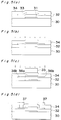
- Figs. 1(a) - (d) illustrate a manufacturing method of a top gate type n-channel thin film transistor of an embodiment according to the present invention.
- a polycrystalline silicon thin film 12 of 100 nm thickness is formed first on a transparent substrate (glass substrate) 11.
- the polycrystalline silicon 12 is etched to form an island as shown in Fig. 1(b), and a silicon oxide thin film 13 of 200 nm thickness is formed as a gate insulator layer.
- boron is introduced in the polycrystalline silicon thin film 12 for the channel region near the interface between the insulator layer 13 and the polycrystalline silicon thin film 12 with the ion doping technique wherein ions are generated by decomposing B2H6 gas on the high frequency discharge without using mass separation of generated ions.
- ions of boron hydrides such as BH x and B2H x and hydrogen ions are generated as well as boron ions, and they are introduced in the sample.
- the acceleration voltage is 30 kV
- the total dose of boron is 1*1014 ions/cm2.
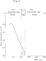
- Fig. 2 shows two examples of the distribution of boron density in the depth direction after boron is introduced in a monocrystalline silicon substrate with the ion doping technique and with the ion implantation technique (comparison example) in conditions of 40 kV of acceleration voltage and 5*1015 ions/cm2 of dose of boron.
- the abscissa represents the depth from the surface of the substrate, while the ordinate represents the boron (impurity) concentration.
- B2H x ions can be generated mainly from B2H6 gas, and a sharp impurity concentration distribution can be realized.
- the impurity concentration to be introduced in the channel region is 1*1018 ions/cm3 of boron
- an insulator layer of 210 nm thickness (refer point A in Fig. 2) is needed to hinder the impurities in the ion doping technique
- that of 350 nm thickness (refer point B in Fig. 2) is needed in the ion implantation technique.
- the thickness of an insulator layer (the gate insulator layer 22 in the present embodiment) needed for the introduction of impurities can be decreased when the same concentration of impurities is introduced, and the characteristics of a device including the thin film transistor can be improved.
- a gate electrode 14 of chromium of 100 nm thickness is formed on the gate insulator layer 13.
- phosphor ions are generated by decomposing PH3 gas by using the high frequency discharge, and they are introduced with use of the gate electrode 14 as a mask into the source and drain regions 14b in the polycrystalline silicon thin film 12 at a high concentration, in the conditions of the acceleration voltage of 80 kV and the dose of the total amount of the impurity ions of 3*1015 ions/cm2.
- the source and drain regions 14b are formed with self-alignment.
- a region between the source and drain regions 14b becomes a channel region 14a eventually.
- the impurity activation annealing of the source and drain regions 14b are performed.
- an inter-layer insulator layer 15 is formed, and contact holes for the source and drain regions 14b are opened.
- hydrogen plasma treatment is carried out to deactivate dangling bonds in the polycrystalline silicon thin film 12 to form the source and drain regions 14b.
- source and drain electrodes 16 are formed through the openings, to complete a thin film transistor.
- a characteristic of the present embodiment is that the impurities are introduced into the channel region 14a for the control of the threshold voltage of the thin film transistor during the manufacturing process, as shown in Fig. 1(c).
- the threshold voltage can be controlled at a desired value by changing the channel doping conditions (acceleration voltage or the total dose of impurities to be introduced).
- the threshold voltage can be changed by 5 V in the ion doping conditions of the acceleration voltage of 35 kV and the dose of boron of 1*1014 ions/cm2.
- the channel doping step is performed after forming the gate insulator layer 13 as shown in Fig. 1(b) in the present embodiment, the sequence of the steps is not limited at the above-mentioned one, and a similar advantage can be obtained when the channel doping step is included during the manufacturing process of thin film transistor.
- the threshold voltage of thin film transistor can be controlled without using the channel doping step if the film thickness of the gate electrode 14 is so thin as to reduce the hinderance of the gate electrode 14 against the ions on forming the source and drain regions 14b, and ions are introduced in the channel region between the source and drain regions 14b to change the concentration difference between the source and drain regions 14b.
- a p-channel thin film transistor can also be manufactured by using appropriate species of impurities.
- the ion beam size is determined only by the size of the ion source, and the introduction to a substrate of wide area becomes easy by enlarging the size of the ion source. Further, the cost of manufacturing can be reduced by the reduction of the cost of the apparatus and the improvement of the throughput.
- a gate electrode 21 made of chromium of 100 nm thickness is formed first on a transparent substrate (glass substrate) 20, and a gate insulator layer 22 of silicon nitride of 400 nm thickness and an amorphous silicon thin film of 50 nm thickness are formed successively on the gate electrode 21 in vacuum with a plasma chemical vapor deposition process (PCVD). Then, the amorphous silicon thin film is crystallized by using the thermal annealing at about 600 °C to form a polycrystalline silicon thin film 23 as a semiconductor active layer.
- PCVD plasma chemical vapor deposition process
- ions of impurities are introduced into source and drain regions in the polycrystalline silicon thin film 23 with an ion doping apparatus. That is, PH3 gas is decomposed on high frequency discharge to generate phosphor ions, and the generated ions are introduced in the source and drain regions 24a, without mass separation, as shown in Fig 3(b).
- the conditions for forming the source and drain regions 24a are as follows: 20 kV of acceleration voltage, and 1*1015 ions/cm2 of total dose of phosphor. Impurities are not introduced into a channel region 24b below the mask 24 between the source and drain regions 24a.
- the polycrystalline silicon is etched to form an island pattern, then the source and drain electrodes 25, 26 are formed on the source and drain regions, as shown in Fig. 3(b).
- a passivation layer 27 of silicon oxide of 200 nm thickness is formed.
- boron is introduced for the control of the threshold voltage from above the passivation layer 27 of insulator into the semiconductor active layer 23 to form a channel region 24b between the source and drain regions 24a.
- the introduced boron is activated in the conditions of 400 °C for 60 minutes, and a thin film transistor is completed.
- An ion doping apparatus is used to introduce boron ions for the control of the threshold voltage, and B2H6 gas is decomposed on high frequency discharge and the generated ions are introduced in the sample without mass separation.
- the conditions for the control of the threshold voltage is as follows: 35 kV of acceleration voltage, and 1*1014/cm2 of dose. Thus, a thin film transistor is completed.
- Fig. 4 shows an example of the impurity distribution after boron is introduced for the control of the threshold voltage along the A-B line displayed in Fig. 3(c). Because the impurities are introduced through the silicon oxide layer 27, most of the impurities remain in the inactive state in the silicon oxide layer 27, and only a very small amount at the tail of the impurity distribution is introduced into the active layer 23 (refer the hatched area in Fig. 4). Thus, the above-mentioned method makes it possible to control the very small amount of impurities beyond the control limit of the ion doping apparatus.
- the damages at the interface between the polycrystalline silicon 23 and the silicon nitride (gate insulator layer) 22 caused by the ion implantation in the prior art method can be suppressed and the characteristics of thin film transistor can be improved.
- the amount of impurities to be introduced in the active layer 23 can be controlled at a desired level by controlling the acceleration voltage and the film thickness of the insulator layer 27. It is found that silicon oxide film is the best as the insulator layer for the control of threshold voltage.
- the threshold voltage of thin film transistor of bottom gate structure can be controlled by changing the introduction conditions of boron. Further, most of the impurities are deactivated in the silicon oxide thin film, and only a tail portion of the impurity distribution is introduced into the active layer. Therefore, the implantation depth into the active layer can be controlled at a desired value by the acceleration voltage on the ion doping and the thickness of the insulator layer on the thin film transistor. In the channel doping conditions according to the example, the threshold voltage varies by about 5 volts.
- thermal annealing is used for crystallizing and for activating the introduced impurities.
- PTA process laser anneal or rapid thermal annealing
- a p-channel thin film transistor can also be manufactured similarly.
- a gate electrode 31 made of chromium of 100 nm thickness is formed first on a transparent substrate (glass substrate) 30, and a gate insulator layer 32 of silicon nitride of 400 nm thickness and a polycrystalline silicon thin film of 50 nm thickness as a semiconductor active layer 33 are formed successively on the gate electrode 31 in vacuum with a plasma chemical vapor deposition process (PCVD). Then, after an island of the polycrystalline silicon thin film is formed, a passivation insulator layer 34 of silicon oxide of 200 nm thickness is formed.
- PCVD plasma chemical vapor deposition process
- boron ions are introduced through the passivation insulator layer 34 into the semiconductor active layer 33 to control the threshold voltage.
- the ions of impurities for the control of the threshold voltage is introduced with an ion doping apparatus. That is, B2H6 gas is decomposed on high frequency discharge to generate boron ions, and the generated ions are introduced in the sample, without mass separation of the generated ions.
- the conditions for the threshold voltage control are as follows: 35 kV of acceleration voltage, and 1 * 1014 ions/cm2 of dose.
- a doping mask 35 is formed with a photoresist, and impurities (boron) are introduced into the source and drain regions 36b.
- impurities boron
- the region between the source and drain regions 36b becomes a channel region 36a eventually.
- the ion doping apparatus is used to introduce the boron ions, and B2H6 gas is decomposed on high frequency discharge and the generated ions are introduced into the source and drain regions 36b without mass separation.
- the conditions for forming the source and drain regions are as follows: 60 kV of acceleration voltage, and 5*1015 ions/cm2 of total dose of impurities. By using the above-mentioned conditions, the threshold voltage can be changed by 5 volts.
- contact holes are formed in the passivation layer 34.
- the plasma treatment is performed to deactivate the dangling bonds in the polycrystalline silicon thin film in the hydrogen plasma, and the source and drain electrodes 37 are formed in the contact holes as shown in Fig. 5(d), to complete a thin film transistor.
- thermal annealing is used for crystallizing and for activating the implanted impurities.
- laser annealing or rapid thermal annealing PTA process
- PTA process rapid thermal annealing
- a p-channel thin film transistor can be manufactured similarly.
- the order of the steps in the example can be changed. For example, similar advantages can be obtained if the steps shown in Figs. 5(b) and (c) are exchanged. Further, similar advantages can be obtained even if the step shown in Fig. 5(b) is omitted and impurities can be introduced after the step shown in Fig. 5(d) by using the conditions mentioned with reference to Fig. 5(b).
- the threshold voltage of the thin film transistor can be controlled at a desired value according to the present invention. Because the ion doping process needs no mass separation of generated ions, the cost of the apparatus is reduced. Further, because it can be applied to a wide area and a high throughput is possible, the manufacturing cost can be reduced.
- the thickness of the insulator layer above the active layer of the thin film transistor suitably, doping of very sharp distribution can be realized without damaging the interface between the channel region and gate insulator layer. Because most of the introduced ions is inactive in the insulator layer and only a very small amount of the implanted ions arrive to the active layer, the implantation at a dose much larger than realized previously becomes possible, and the controllability of the threshold voltage can be improved. The cost of the apparatus is reduced by sharing the apparatus commonly in the steps for introducing impurity ions.
- the present invention by introducing a very small amount of ionized impurities from above the insulator layer into the semiconductor layer to control the threshold voltage, most of the implanted impurities lose an energy in the insulator layer to stop and to be deactivated electrically. Thus, only a portion of the impurities at the tail of the impurity profile is introduced into the semiconductor active layer. Further, the film thickness of the insulator layer can be changed. Then, the depth of the impurity distribution and the amount of the impurities can be controlled at desired values.
Abstract
In a manufacturing method of thin film transistor, when impurity ions are introduced in a channel region between source and drain regions in a semiconductor layer, an insulator layer is formed on the semiconductor layer first. Then, impurity ions generated on high frequency discharge are introduced through the insulator layer into the semiconductor layer under a specified acceleration voltage. Then, the introduction depth of impurities and the amount of the impurities to be introduced in the channel region can be controlled or the threshold voltage of the thin film transistor can be controlled. This method can be applied to a large substrate.
Description
- The present invention relates to a method for manufacturing a thin film transistor and semiconductor devices such as a liquid crystal display, an image sensor and a memory including thin film transistors.
- In a semiconductor device such as a liquid crystal display or an image sensor with use of thin film transistors, the control of the threshold voltage of the thin film transistor is important. Especially for an active-matrix type liquid crystal display which includes peripheral circuits, it is necessary to control the threshold voltages of p- and n-channel thin film transistors in the periphery circuits for decreasing the dissipation of electric power and for driving at a faster rate. The threshold voltage is mainly controlled by the state at the interface between the semiconductor active layer and the gate insulator layer in the thin film transistor, and it is not easy to control the threshold voltage in a wide range.
- Previously, channel doping technique is used for controlling the threshold voltage of thin film transistor. In the channel doping technique, the ion implantation process is used to introduce a very small amount of impurities into a semiconductor active layer. However, the size of the ion beam is small in the prior art technique. When impurities are introduced to a substrate of large area as used for a liquid crystal display or the like, the ion beam has to scan over the large substrate, and this limits the area to be processed and the throughput of the processing. Therefore, it is difficult to adopt the ion implantation for manufacturing thin film transistors on a large substrate. Further, if the ion implantation is carried out on an insulator substrate such as a silica or glass plate, a charge up phenomenon occurs or the substrate is charged due to the implanted ions, and this lowers the precision of the implantation. Therefore, it is needed to introduce impurities while preventing the charge up of the substrate.
- An object of the present invention is to provide a method for controlling the threshold level of thin film transistor at a desired level.
- In a manufacturing method of thin film transistor, when impurity ions are introduced in the channel region between the source and drain regions, first an insulator layer is formed on a non-monocrystalline thin film of semiconductor material. Then, impurity ions generated on high frequency discharge are introduced through the insulator layer into the semiconductor layer under a specified acceleration voltage. Then, the introduction depth of impurities and the amount of the impurities to be introduced in the channel region can be controlled or the threshold voltage of the thin film transistor can be controlled. That is, the impurities are introduced without using mass separation of the ions. In order to improve the controllability of the threshold voltage, the acceleration voltage on the introduction into the non-monocrystalline thin film is preferably 80 kV or less or the dose of the impurity ions for controlling the valence electrons is preferably 5*10¹⁵ ion/cm² or less.
- An advantage of the present invention is that ions can be introduced into the channel region of the thin film transistor on a large substrate.
- These and other objects and features of the present invention will become clear from the following description taken in conjunction with the preferred embodiments thereof with reference to the accompanying drawings, and in which:
- Figs. 1(a) - (d) are sectional views for illustrating an example of a first embodiment a manufacturing method of a top gate type thin film transistor;
- Fig. 2 is a graph of the distribution of the implanted ions;
- Figs. 3(a) - (c) are sectional views for illustrating a manufacturing method of a first example of a second embodiment of a bottom gate type thin film transistor;
- Fig. 4 is a graph of the distribution of the boron density along A-B line in Fig. 3(c); and
- Figs. 5(a) - (d) are sectional views for illustrating a manufacturing method of a second example of the second embodiment of a bottom gate type thin film transistor.
- Referring now to the drawings, wherein like reference characters designate like or corresponding parts throughout the several views, embodiments of the present invention are explained below.
- In order to solve the above-mentioned problems, a technique called as ion doping or ion shower doping is adopted in the present invention (refer IEEE Electron Devices Letters, Vol. 9, No. 2, 1988, 90 - 93 on the technique). A gas including impurities to be introduced as constituent elements thereof is ionized by using high frequency discharge, and the ionized impurities to be introduced in a sample are all accelerated at a specified acceleration voltage. In the present invention, generated ions are all introduced into a sample without using mass separation of the generated ions as in the prior art ion implantation. Because mass production is not needed, the size of ion beam can be increased as large as the size of the ion generator. Thus, the ion beam size can be increased remarkably larger than that in the prior art, and the impurities can be introduced over a large substrate at a fast rate.
- Figs. 1(a) - (d) illustrate a manufacturing method of a top gate type n-channel thin film transistor of an embodiment according to the present invention. As shown in Fig. 1(a), a polycrystalline silicon
thin film 12 of 100 nm thickness is formed first on a transparent substrate (glass substrate) 11. Next, thepolycrystalline silicon 12 is etched to form an island as shown in Fig. 1(b), and a silicon oxidethin film 13 of 200 nm thickness is formed as a gate insulator layer. Then, boron is introduced in the polycrystalline siliconthin film 12 for the channel region near the interface between theinsulator layer 13 and the polycrystalline siliconthin film 12 with the ion doping technique wherein ions are generated by decomposing B₂H₆ gas on the high frequency discharge without using mass separation of generated ions. At the decomposition of the B₂H₆ gas, ions of boron hydrides such as BHx and B₂Hx and hydrogen ions are generated as well as boron ions, and they are introduced in the sample. On introducing boron in the polycrystalline siliconthin film 12, the acceleration voltage is 30 kV, and the total dose of boron is 1*10¹⁴ ions/cm². - Fig. 2 shows two examples of the distribution of boron density in the depth direction after boron is introduced in a monocrystalline silicon substrate with the ion doping technique and with the ion implantation technique (comparison example) in conditions of 40 kV of acceleration voltage and 5*10¹⁵ ions/cm² of dose of boron. The abscissa represents the depth from the surface of the substrate, while the ordinate represents the boron (impurity) concentration. In case of ion doping, B₂Hx ions can be generated mainly from B₂H₆ gas, and a sharp impurity concentration distribution can be realized. For example, if the impurity concentration to be introduced in the channel region is 1*10¹⁸ ions/cm³ of boron, an insulator layer of 210 nm thickness (refer point A in Fig. 2) is needed to hinder the impurities in the ion doping technique, whereas that of 350 nm thickness (refer point B in Fig. 2) is needed in the ion implantation technique. Thus, by using the ion doping technique, the thickness of an insulator layer (the
gate insulator layer 22 in the present embodiment) needed for the introduction of impurities can be decreased when the same concentration of impurities is introduced, and the characteristics of a device including the thin film transistor can be improved. - As shown in Fig. 1(c), after the activation annealing of the introduced boron is performed at 400 °C for 60 minutes, a
gate electrode 14 of chromium of 100 nm thickness is formed on thegate insulator layer 13. Next, phosphor ions are generated by decomposing PH₃ gas by using the high frequency discharge, and they are introduced with use of thegate electrode 14 as a mask into the source anddrain regions 14b in the polycrystalline siliconthin film 12 at a high concentration, in the conditions of the acceleration voltage of 80 kV and the dose of the total amount of the impurity ions of 3*10¹⁵ ions/cm². The source anddrain regions 14b are formed with self-alignment. Thus, a region between the source anddrain regions 14b becomes a channel region 14a eventually. Next, the impurity activation annealing of the source anddrain regions 14b are performed. Then, as shown in Fig. 1(d), aninter-layer insulator layer 15 is formed, and contact holes for the source anddrain regions 14b are opened. Next, hydrogen plasma treatment is carried out to deactivate dangling bonds in the polycrystalline siliconthin film 12 to form the source anddrain regions 14b. Finally, source anddrain electrodes 16 are formed through the openings, to complete a thin film transistor. - A characteristic of the present embodiment is that the impurities are introduced into the channel region 14a for the control of the threshold voltage of the thin film transistor during the manufacturing process, as shown in Fig. 1(c). The threshold voltage can be controlled at a desired value by changing the channel doping conditions (acceleration voltage or the total dose of impurities to be introduced). In the present embodiment, the threshold voltage can be changed by 5 V in the ion doping conditions of the acceleration voltage of 35 kV and the dose of boron of 1*10¹⁴ ions/cm².
- Though the channel doping step is performed after forming the
gate insulator layer 13 as shown in Fig. 1(b) in the present embodiment, the sequence of the steps is not limited at the above-mentioned one, and a similar advantage can be obtained when the channel doping step is included during the manufacturing process of thin film transistor. Further, the threshold voltage of thin film transistor can be controlled without using the channel doping step if the film thickness of thegate electrode 14 is so thin as to reduce the hinderance of thegate electrode 14 against the ions on forming the source anddrain regions 14b, and ions are introduced in the channel region between the source anddrain regions 14b to change the concentration difference between the source anddrain regions 14b. - Though an n-channel thin film transistor is manufactured in the above-mentioned embodiment, a p-channel thin film transistor can also be manufactured by using appropriate species of impurities.
- By using the ion source, the ion beam size is determined only by the size of the ion source, and the introduction to a substrate of wide area becomes easy by enlarging the size of the ion source. Further, the cost of manufacturing can be reduced by the reduction of the cost of the apparatus and the improvement of the throughput.
- Next, an example of a second embodiment of a manufacturing method of a bottom gate type thin film transistor is explained below with reference to Figs. 3(a) - (c). As shown in Fig. 3(a), a
gate electrode 21 made of chromium of 100 nm thickness is formed first on a transparent substrate (glass substrate) 20, and agate insulator layer 22 of silicon nitride of 400 nm thickness and an amorphous silicon thin film of 50 nm thickness are formed successively on thegate electrode 21 in vacuum with a plasma chemical vapor deposition process (PCVD). Then, the amorphous silicon thin film is crystallized by using the thermal annealing at about 600 °C to form a polycrystalline silicon thin film 23 as a semiconductor active layer. Then, after adoping mask 24 is formed on the polycrystalline silicon thin film 23, ions of impurities (phosphor in this case) are introduced into source and drain regions in the polycrystalline silicon thin film 23 with an ion doping apparatus. That is, PH₃ gas is decomposed on high frequency discharge to generate phosphor ions, and the generated ions are introduced in the source anddrain regions 24a, without mass separation, as shown in Fig 3(b). The conditions for forming the source anddrain regions 24a are as follows: 20 kV of acceleration voltage, and 1*10¹⁵ ions/cm² of total dose of phosphor. Impurities are not introduced into achannel region 24b below themask 24 between the source anddrain regions 24a. After the activation annealing of the implanted impurities, the polycrystalline silicon is etched to form an island pattern, then the source and drainelectrodes - Next, as shown in Fig. 3(c), a
passivation layer 27 of silicon oxide of 200 nm thickness is formed. After the plasma treatment in the hydrogen plasma to deactivate the dangling bonds in the polycrystalline silicon thin film 23, boron is introduced for the control of the threshold voltage from above thepassivation layer 27 of insulator into the semiconductor active layer 23 to form achannel region 24b between the source anddrain regions 24a. The introduced boron is activated in the conditions of 400 °C for 60 minutes, and a thin film transistor is completed. An ion doping apparatus is used to introduce boron ions for the control of the threshold voltage, and B₂H₆ gas is decomposed on high frequency discharge and the generated ions are introduced in the sample without mass separation. The conditions for the control of the threshold voltage is as follows: 35 kV of acceleration voltage, and 1*10¹⁴/cm² of dose. Thus, a thin film transistor is completed. - Fig. 4 shows an example of the impurity distribution after boron is introduced for the control of the threshold voltage along the A-B line displayed in Fig. 3(c). Because the impurities are introduced through the
silicon oxide layer 27, most of the impurities remain in the inactive state in thesilicon oxide layer 27, and only a very small amount at the tail of the impurity distribution is introduced into the active layer 23 (refer the hatched area in Fig. 4). Thus, the above-mentioned method makes it possible to control the very small amount of impurities beyond the control limit of the ion doping apparatus. Further, the damages at the interface between the polycrystalline silicon 23 and the silicon nitride (gate insulator layer) 22 caused by the ion implantation in the prior art method can be suppressed and the characteristics of thin film transistor can be improved. It is to be noted that the amount of impurities to be introduced in the active layer 23 can be controlled at a desired level by controlling the acceleration voltage and the film thickness of theinsulator layer 27. It is found that silicon oxide film is the best as the insulator layer for the control of threshold voltage. - By using the above-mentioned manufacturing method, the threshold voltage of thin film transistor of bottom gate structure can be controlled by changing the introduction conditions of boron. Further, most of the impurities are deactivated in the silicon oxide thin film, and only a tail portion of the impurity distribution is introduced into the active layer. Therefore, the implantation depth into the active layer can be controlled at a desired value by the acceleration voltage on the ion doping and the thickness of the insulator layer on the thin film transistor. In the channel doping conditions according to the example, the threshold voltage varies by about 5 volts.
- Further, in the example shown in Figs. 3(a) - (c), thermal annealing is used for crystallizing and for activating the introduced impurities. However, similar advantages can be realized with laser anneal or rapid thermal annealing (PTA process). When a laser is used, after the impurities are introduced into the source and drain regions, the crystallization of the semiconductor active layer can be performed at the same time as the activation of the impurities in the source and drain regions. Thus, the manufacturing process can be simplified.
- Though the manufacturing method of n-channel thin film transistor is explained above, a p-channel thin film transistor can also be manufactured similarly.
- Next, a second example of the second embodiment of the manufacturing method of bottom gate type thin film transistor is explained below with reference to Figs. 5(a) - (d). As shown in Fig. 5(a), a
gate electrode 31 made of chromium of 100 nm thickness is formed first on a transparent substrate (glass substrate) 30, and agate insulator layer 32 of silicon nitride of 400 nm thickness and a polycrystalline silicon thin film of 50 nm thickness as a semiconductoractive layer 33 are formed successively on thegate electrode 31 in vacuum with a plasma chemical vapor deposition process (PCVD). Then, after an island of the polycrystalline silicon thin film is formed, apassivation insulator layer 34 of silicon oxide of 200 nm thickness is formed. Next, as shown in Fig. 5(b), boron ions are introduced through thepassivation insulator layer 34 into the semiconductoractive layer 33 to control the threshold voltage. The ions of impurities for the control of the threshold voltage is introduced with an ion doping apparatus. That is, B₂H₆ gas is decomposed on high frequency discharge to generate boron ions, and the generated ions are introduced in the sample, without mass separation of the generated ions. The conditions for the threshold voltage control are as follows: 35 kV of acceleration voltage, and 1 * 10¹⁴ ions/cm² of dose. - Next, as shown in Fig. 5(c), a doping mask 35 is formed with a photoresist, and impurities (boron) are introduced into the source and drain
regions 36b. The region between the source and drainregions 36b becomes achannel region 36a eventually. The ion doping apparatus is used to introduce the boron ions, and B₂H₆ gas is decomposed on high frequency discharge and the generated ions are introduced into the source and drainregions 36b without mass separation. The conditions for forming the source and drain regions are as follows: 60 kV of acceleration voltage, and 5*10¹⁵ ions/cm² of total dose of impurities. By using the above-mentioned conditions, the threshold voltage can be changed by 5 volts. - After the activation annealing of the impurities at 400 °C for 60 minutes, contact holes are formed in the
passivation layer 34. Then, the plasma treatment is performed to deactivate the dangling bonds in the polycrystalline silicon thin film in the hydrogen plasma, and the source and drainelectrodes 37 are formed in the contact holes as shown in Fig. 5(d), to complete a thin film transistor. - Further, in the second example explained above, thermal annealing is used for crystallizing and for activating the implanted impurities. However, laser annealing or rapid thermal annealing (PTA process) can also be used. When a laser is used, after the impurities are introduced into the source and drain regions, the crystallization of the semiconductor active layer can be performed at the same time as the activation of the impurities in the source and drain regions. Thus, the manufacturing process can be simplified.
- Though the manufacturing method of n-channel thin film transistor is explained above, a p-channel thin film transistor can be manufactured similarly. The order of the steps in the example can be changed. For example, similar advantages can be obtained if the steps shown in Figs. 5(b) and (c) are exchanged. Further, similar advantages can be obtained even if the step shown in Fig. 5(b) is omitted and impurities can be introduced after the step shown in Fig. 5(d) by using the conditions mentioned with reference to Fig. 5(b).
- The threshold voltage of the thin film transistor can be controlled at a desired value according to the present invention. Because the ion doping process needs no mass separation of generated ions, the cost of the apparatus is reduced. Further, because it can be applied to a wide area and a high throughput is possible, the manufacturing cost can be reduced.
- By setting the thickness of the insulator layer above the active layer of the thin film transistor suitably, doping of very sharp distribution can be realized without damaging the interface between the channel region and gate insulator layer. Because most of the introduced ions is inactive in the insulator layer and only a very small amount of the implanted ions arrive to the active layer, the implantation at a dose much larger than realized previously becomes possible, and the controllability of the threshold voltage can be improved. The cost of the apparatus is reduced by sharing the apparatus commonly in the steps for introducing impurity ions.
- In the present invention, by introducing a very small amount of ionized impurities from above the insulator layer into the semiconductor layer to control the threshold voltage, most of the implanted impurities lose an energy in the insulator layer to stop and to be deactivated electrically. Thus, only a portion of the impurities at the tail of the impurity profile is introduced into the semiconductor active layer. Further, the film thickness of the insulator layer can be changed. Then, the depth of the impurity distribution and the amount of the impurities can be controlled at desired values.
- Although the present invention has been fully described in connection with the preferred embodiments thereof with reference to the accompanying drawings, it is to be noted that various changes and modifications are apparent to those skilled in the art. Such changes and modifications are to be understood as included within the scope of the present invention as defined by the appended claims unless they depart therefrom.
Claims (19)
- A method for manufacturing a thin film transistor, comprising the steps of:
forming a non-monocrystalline thin film of a semiconductor material on a substrate;
forming a first insulator layer on the non-monocrystalline film and the substrate;
introducing ions of impurities through the first insulator layer into the non-monocrystalline thin film under a specified acceleration voltage whereby the ions introduced in the non-monocrystalline thin film control the threshold voltage of the thin film transistor;
forming a gate electrode on the first insulator layer;
forming source and drain regions in the non-monocrystalline thin film by introducing impurities for the source and drain regions;
forming a second insulator film on the gate electrode and the first insulator film; and
forming source and drain electrodes connected electrically to the source and drain regions. - The method according to Claim 1, wherein said source and drain regions are introduced into said non-monocrystalline thin film through said first insulator layer by using said gate electrode as a mask.
- The method according to Claim 1, wherein said second insulator layer formed on said non-monocrystalline thin film is made of silicon oxide.
- The method according to Claim 1, wherein the ions to be introduced into said non-monocrystalline thin film are generated by decomposing a gas with high frequency discharge.
- The method according to Claim 4, wherein said gas includes boron.
- The method according to Claim 4, wherein said gas includes phosphor.
- The method according to Claim 1, wherein said acceleration voltage is 80 kV or less.
- The method according to Claim 1, wherein the dose of the impurity ions for said non-monocrystalline thin film is 5*10¹⁵ ions/cm² or less.
- The method according to Claim 1, wherein said non-monocrystalline thin film is made of polycrystalline silicon.
- A method for manufacturing a thin film transistor comprising the steps of:
forming a gate electrode on a substrate;
forming a first insulator layer on the gate electrode and the substrate;
forming a non-monocrystalline thin film on a first insulator layer above the gate electrode;
forming source and drain regions in the non-monocrystalline thin film by introducing impurities for the source and drain regions;
forming a second insulator layer on the non-monocrystalline thin film; and
introducing ions of impurities for forming a channel region between the source and drain regions in the non-monocrystalline thin film through the second insulator layer into the non-monocrystalline thin film under a specified acceleration voltage whereby the ions introduced in the non-monocrystalline thin film control the threshold voltage of the thin film transistor. - The method according to Claim 10, wherein said ions of impurities for forming said source and drain regions are introduced by using a mask formed on said non-monocrystalline thin film, wherein the source and drain regions are formed in a self-alignment condition by using the mask, and said ions of impurities for forming said channel region are introduced after the mask is removed.
- The method according to Claim 10, wherein said step of forming said source and drain regions is performed by using a mask formed on said non-monocrystalline thin film above said gate electrode after said ions for forming said channel region are introduced into the thin film transistor.
- The method according to Claim 10, wherein said second insulator layer formed on said non-monocrystalline thin film is made of silicon oxide.
- The method according to Claim 10, wherein the ions to be introduced into said non-monocrystalline thin film are generated by decomposing a gas with high frequency discharge.
- The method according to Claim 14, wherein said gas includes boron.
- The method according to Claim 14, wherein said gas includes phosphor.
- The method according to Claim 10, wherein said acceleration voltage is 80 kV or less.
- The method according to Claim 10, wherein the dose of the impurity ions for said channel region is 5*10¹⁵ ions/cm² or less.
- The method according to Claim 10, wherein said non-monocrystalline thin film is made of polycrystalline silicon.
Applications Claiming Priority (4)
| Application Number | Priority Date | Filing Date | Title |
|---|---|---|---|
| JP34660/92 | 1992-02-21 | ||
| JP3466092A JP2970176B2 (en) | 1992-02-21 | 1992-02-21 | Method of manufacturing thin film transistor and liquid crystal display device using the thin film transistor |
| JP20583692A JPH0653507A (en) | 1992-08-03 | 1992-08-03 | Fabrication of thin film transistor and semiconductor device employing thin film transistor |
| JP205836/92 | 1992-08-03 |
Publications (2)
| Publication Number | Publication Date |
|---|---|
| EP0566838A2 true EP0566838A2 (en) | 1993-10-27 |
| EP0566838A3 EP0566838A3 (en) | 1996-07-31 |
Family
ID=26373491
Family Applications (1)
| Application Number | Title | Priority Date | Filing Date |
|---|---|---|---|
| EP93102520A Withdrawn EP0566838A3 (en) | 1992-02-21 | 1993-02-18 | Manufacturing method of thin film transistor |
Country Status (2)
| Country | Link |
|---|---|
| US (1) | US5397718A (en) |
| EP (1) | EP0566838A3 (en) |
Cited By (7)
| Publication number | Priority date | Publication date | Assignee | Title |
|---|---|---|---|---|
| FR2747237A1 (en) * | 1996-04-09 | 1997-10-10 | Lg Electronics Inc | LIQUID CRYSTAL DISPLAY DEVICE AND METHOD FOR MANUFACTURING THE SAME |
| EP0989614A2 (en) | 1998-09-04 | 2000-03-29 | Sel Semiconductor Energy Laboratory Co., Ltd. | TFT with an LDD structure and its manufacturing method |
| EP1017108A2 (en) * | 1998-12-25 | 2000-07-05 | Semiconductor Energy Laboratory Co., Ltd. | Semiconductor devices and methods of manufacturing the same |
| CN1103117C (en) * | 1997-02-06 | 2003-03-12 | 日本电气株式会社 | Manufacturing engineering for field effect transistor capable of changing its threshold voltage by hydrion |
| WO2003067666A1 (en) * | 2002-02-07 | 2003-08-14 | Matsushita Electric Industrial Co., Ltd. | Semiconductor device and method for fabricating the same |
| US6891236B1 (en) | 1999-01-14 | 2005-05-10 | Semiconductor Energy Laboratory Co., Ltd. | Semiconductor device and method of fabricating the same |
| CN100334743C (en) * | 1994-08-19 | 2007-08-29 | 株式会社半导体能源研究所 | Semiconductor device and its manufacture |
Families Citing this family (21)
| Publication number | Priority date | Publication date | Assignee | Title |
|---|---|---|---|---|
| US6964890B1 (en) | 1992-03-17 | 2005-11-15 | Semiconductor Energy Laboratory Co., Ltd. | Semiconductor device and method for forming the same |
| JP2912506B2 (en) * | 1992-10-21 | 1999-06-28 | シャープ株式会社 | Method for forming transparent conductive film |
| US5403762A (en) * | 1993-06-30 | 1995-04-04 | Semiconductor Energy Laboratory Co., Ltd. | Method of fabricating a TFT |
| US6323071B1 (en) * | 1992-12-04 | 2001-11-27 | Semiconductor Energy Laboratory Co., Ltd. | Method for forming a semiconductor device |
| US5543335A (en) * | 1993-05-05 | 1996-08-06 | Ixys Corporation | Advanced power device process for low drop |
| US5477073A (en) * | 1993-08-20 | 1995-12-19 | Casio Computer Co., Ltd. | Thin film semiconductor device including a driver and a matrix circuit |
| JPH07142743A (en) * | 1993-09-22 | 1995-06-02 | Sharp Corp | Manufacture of thin-film transistor |
| KR100319332B1 (en) * | 1993-12-22 | 2002-04-22 | 야마자끼 순페이 | Semiconductor device and electro-optical device |
| US5976919A (en) * | 1994-06-10 | 1999-11-02 | Matsushita Electric Industrial Co., Ltd. | Apparatus and method of manufacturing semiconductor element |
| JP3176527B2 (en) * | 1995-03-30 | 2001-06-18 | シャープ株式会社 | Method for manufacturing semiconductor device |
| US6933182B1 (en) * | 1995-04-20 | 2005-08-23 | Semiconductor Energy Laboratory Co., Ltd. | Method of manufacturing a semiconductor device and manufacturing system thereof |
| US5721163A (en) * | 1996-06-10 | 1998-02-24 | Chartered Semiconductor Manufacturing Pte, Ltd. | Method of manufacture of thin film transistor SRAM device with a titanium nitride or silicide gate |
| JP3323889B2 (en) * | 1996-10-28 | 2002-09-09 | 三菱電機株式会社 | Method for manufacturing thin film transistor |
| US6197624B1 (en) * | 1997-08-29 | 2001-03-06 | Semiconductor Energy Laboratory Co., Ltd. | Method of adjusting the threshold voltage in an SOI CMOS |
| JPH11112002A (en) * | 1997-10-07 | 1999-04-23 | Semiconductor Energy Lab Co Ltd | Semiconductor device and manufacture therefor |
| JP3968484B2 (en) * | 1998-02-18 | 2007-08-29 | ソニー株式会社 | Thin film transistor manufacturing method |
| JP4869509B2 (en) * | 2001-07-17 | 2012-02-08 | 株式会社半導体エネルギー研究所 | Method for manufacturing semiconductor device |
| KR100682893B1 (en) * | 2004-10-13 | 2007-02-15 | 삼성전자주식회사 | Thin film transistor and method of manufacturing the same |
| KR100749010B1 (en) * | 2005-12-26 | 2007-08-13 | (주)포인트엔지니어링 | POLY CRYSTALLINE Si THIN FILM FABRICATION METHOD AND APPARATUS USING TRANSPARENT SUBSTRATE |
| TWI305682B (en) * | 2006-08-14 | 2009-01-21 | Au Optronics Corp | Bottom substrate for liquid crystal display device and the method of making the same |
| US8354674B2 (en) * | 2007-06-29 | 2013-01-15 | Semiconductor Energy Laboratory Co., Ltd. | Semiconductor device wherein a property of a first semiconductor layer is different from a property of a second semiconductor layer |
Citations (8)
| Publication number | Priority date | Publication date | Assignee | Title |
|---|---|---|---|---|
| JPS5830123A (en) * | 1981-08-18 | 1983-02-22 | Toshiba Corp | Manufacture of semiconductor device |
| JPS62219574A (en) * | 1986-03-19 | 1987-09-26 | Sharp Corp | Semiconductor device |
| JPS6329978A (en) * | 1986-07-23 | 1988-02-08 | Sharp Corp | Manufacture of thin-film transistor |
| JPH01276768A (en) * | 1988-04-28 | 1989-11-07 | Fujitsu Ltd | Manufacture of thin film transistor |
| EP0361609A2 (en) * | 1988-09-30 | 1990-04-04 | Philips Electronics Uk Limited | Thin-film transistors, their method of manufacture, and display device using such transistors |
| JPH02123743A (en) * | 1988-11-02 | 1990-05-11 | Fujitsu Ltd | Manufacture of thin film transistor |
| EP0383230A2 (en) * | 1989-02-14 | 1990-08-22 | Seiko Epson Corporation | Manufacturing Method of a Semiconductor Device |
| JPH0439967A (en) * | 1990-06-05 | 1992-02-10 | Matsushita Electric Ind Co Ltd | Manufacture of thin-film transistor |
Family Cites Families (17)
| Publication number | Priority date | Publication date | Assignee | Title |
|---|---|---|---|---|
| JPS5421180A (en) * | 1977-07-19 | 1979-02-17 | Fujitsu Ltd | Semiconductor device |
| US4312680A (en) * | 1980-03-31 | 1982-01-26 | Rca Corporation | Method of manufacturing submicron channel transistors |
| JPS5856409A (en) * | 1981-09-30 | 1983-04-04 | Toshiba Corp | Production of semiconductor device |
| JPS58206121A (en) * | 1982-05-27 | 1983-12-01 | Toshiba Corp | Manufacture of thin-film semiconductor device |
| JPS59159563A (en) * | 1983-03-02 | 1984-09-10 | Toshiba Corp | Manufacture of semiconductor device |
| JPS60128668A (en) * | 1983-12-15 | 1985-07-09 | Toshiba Corp | Manufacture of semiconductor device |
| JPS6148979A (en) * | 1984-08-17 | 1986-03-10 | Seiko Epson Corp | Manufacture of polycrystalline silicon thin-film transistor |
| JPS63283068A (en) * | 1987-05-14 | 1988-11-18 | Sharp Corp | Manufacture of thin-film transistor |
| US4992838A (en) * | 1988-02-29 | 1991-02-12 | Texas Instruments Incorporated | Vertical MOS transistor with threshold voltage adjustment |
| US4951113A (en) * | 1988-11-07 | 1990-08-21 | Xerox Corporation | Simultaneously deposited thin film CMOS TFTs and their method of fabrication |
| US5116771A (en) * | 1989-03-20 | 1992-05-26 | Massachusetts Institute Of Technology | Thick contacts for ultra-thin silicon on insulator films |
| JPH03276765A (en) * | 1990-03-27 | 1991-12-06 | Nec Corp | Manufacture of semiconductor integrated circuit |
| US5198379A (en) * | 1990-04-27 | 1993-03-30 | Sharp Kabushiki Kaisha | Method of making a MOS thin film transistor with self-aligned asymmetrical structure |
| JPH0494133A (en) * | 1990-08-10 | 1992-03-26 | Fuji Xerox Co Ltd | Manufacture of thin film semiconductor device |
| US5064775A (en) * | 1990-09-04 | 1991-11-12 | Industrial Technology Research Institute | Method of fabricating an improved polycrystalline silicon thin film transistor |
| JPH04134831A (en) * | 1990-09-27 | 1992-05-08 | Oki Electric Ind Co Ltd | Manufacture of mos semiconductor device |
| US5252502A (en) * | 1992-08-03 | 1993-10-12 | Texas Instruments Incorporated | Method of making MOS VLSI semiconductor device with metal gate |
-
1993
- 1993-02-18 EP EP93102520A patent/EP0566838A3/en not_active Withdrawn
- 1993-02-19 US US08/019,682 patent/US5397718A/en not_active Expired - Lifetime
Patent Citations (8)
| Publication number | Priority date | Publication date | Assignee | Title |
|---|---|---|---|---|
| JPS5830123A (en) * | 1981-08-18 | 1983-02-22 | Toshiba Corp | Manufacture of semiconductor device |
| JPS62219574A (en) * | 1986-03-19 | 1987-09-26 | Sharp Corp | Semiconductor device |
| JPS6329978A (en) * | 1986-07-23 | 1988-02-08 | Sharp Corp | Manufacture of thin-film transistor |
| JPH01276768A (en) * | 1988-04-28 | 1989-11-07 | Fujitsu Ltd | Manufacture of thin film transistor |
| EP0361609A2 (en) * | 1988-09-30 | 1990-04-04 | Philips Electronics Uk Limited | Thin-film transistors, their method of manufacture, and display device using such transistors |
| JPH02123743A (en) * | 1988-11-02 | 1990-05-11 | Fujitsu Ltd | Manufacture of thin film transistor |
| EP0383230A2 (en) * | 1989-02-14 | 1990-08-22 | Seiko Epson Corporation | Manufacturing Method of a Semiconductor Device |
| JPH0439967A (en) * | 1990-06-05 | 1992-02-10 | Matsushita Electric Ind Co Ltd | Manufacture of thin-film transistor |
Non-Patent Citations (9)
| Title |
|---|
| ELECTRONICS & COMMUNICATIONS IN JAPAN, PART II - ELECTRONICS, vol. 71, no. 10, PART 2, pages 40-45, XP000043970 HIRANO R ET AL: "FABRICATION OF POLYCRYSTALLINE SILICON THIN-FILM TRANSISTORS BY ION SHOWER DOPING TECHNIQUE" * |
| JAPANESE JOURNAL OF APPLIED PHYSICS, vol. 29, no. 12 PART 01, 1 December 1990, pages 2705-2710, XP000263386 KIKUO ONO ET AL: "EFFECT OF CHANNEL IMPLANTATION ON THE DEVICE PERFORMANCE OF LOW TEMPERATURE PROCESSED POLYCRYSTALLINE SILICON THIN FILM TRANSISTORS" * |
| PATENT ABSTRACTS OF JAPAN vol. 007, no. 107 (E-174), 11 May 1983 & JP-A-58 030123 (TOKYO SHIBAURA DENKI KK), 22 February 1983, * |
| PATENT ABSTRACTS OF JAPAN vol. 012, no. 080 (E-590), 12 March 1988 & JP-A-62 219574 (SHARP CORP), 26 September 1987, * |
| PATENT ABSTRACTS OF JAPAN vol. 012, no. 239 (E-630), 7 July 1988 & JP-A-63 029978 (SHARP CORP), 8 February 1988, * |
| PATENT ABSTRACTS OF JAPAN vol. 014, no. 045 (E-0880), 26 January 1990 & JP-A-01 276768 (FUJITSU LTD), 7 November 1989, * |
| PATENT ABSTRACTS OF JAPAN vol. 014, no. 354 (E-0958), 31 July 1990 & JP-A-02 123743 (FUJITSU LTD), 11 May 1990, * |
| PATENT ABSTRACTS OF JAPAN vol. 016, no. 224 (E-1206), 25 May 1992 & JP-A-04 039967 (MATSUSHITA ELECTRIC IND CO LTD), 10 February 1992, & US-A-5 141 885 25 August 1992 * |
| PROCEEDINGS OF THE INTERNATIONAL ELECTRON DEVICES MEETING, WASHINGTON,, 8 - 11 December 1991, INSTITUTE OF ELECTRICAL AND ELECTRONICS ENGINEERS, pages 555-558, XP000342189 SATOSHI INOUE ET AL: "LOW TEMPERATURE CMOS SELF-ALIGNED POLY-SI TFTS AND CIRCUIT SCHEME UTILIZING NEW ION DOPING AND MASKING TECHNIQUE" * |
Cited By (10)
| Publication number | Priority date | Publication date | Assignee | Title |
|---|---|---|---|---|
| CN100334743C (en) * | 1994-08-19 | 2007-08-29 | 株式会社半导体能源研究所 | Semiconductor device and its manufacture |
| FR2747237A1 (en) * | 1996-04-09 | 1997-10-10 | Lg Electronics Inc | LIQUID CRYSTAL DISPLAY DEVICE AND METHOD FOR MANUFACTURING THE SAME |
| CN1103117C (en) * | 1997-02-06 | 2003-03-12 | 日本电气株式会社 | Manufacturing engineering for field effect transistor capable of changing its threshold voltage by hydrion |
| EP0989614A2 (en) | 1998-09-04 | 2000-03-29 | Sel Semiconductor Energy Laboratory Co., Ltd. | TFT with an LDD structure and its manufacturing method |
| EP0989614A3 (en) * | 1998-09-04 | 2009-06-10 | Sel Semiconductor Energy Laboratory Co., Ltd. | TFT with an LDD structure and its manufacturing method |
| EP1017108A2 (en) * | 1998-12-25 | 2000-07-05 | Semiconductor Energy Laboratory Co., Ltd. | Semiconductor devices and methods of manufacturing the same |
| EP1017108A3 (en) * | 1998-12-25 | 2001-01-24 | Semiconductor Energy Laboratory Co., Ltd. | Semiconductor devices and methods of manufacturing the same |
| US6891236B1 (en) | 1999-01-14 | 2005-05-10 | Semiconductor Energy Laboratory Co., Ltd. | Semiconductor device and method of fabricating the same |
| US7491655B2 (en) | 1999-01-14 | 2009-02-17 | Semiconductor Energy Laboratory Co., Ltd. | Semiconductor device and method of fabricating the same |
| WO2003067666A1 (en) * | 2002-02-07 | 2003-08-14 | Matsushita Electric Industrial Co., Ltd. | Semiconductor device and method for fabricating the same |
Also Published As
| Publication number | Publication date |
|---|---|
| US5397718A (en) | 1995-03-14 |
| EP0566838A3 (en) | 1996-07-31 |
Similar Documents
| Publication | Publication Date | Title |
|---|---|---|
| US5397718A (en) | Method of manufacturing thin film transistor | |
| US5373803A (en) | Method of epitaxial growth of semiconductor | |
| US5180690A (en) | Method of forming a layer of doped crystalline semiconductor alloy material | |
| JP2796175B2 (en) | Method for manufacturing thin film transistor | |
| EP0494628A2 (en) | Multigato SOI-type thin film transistor and manufacturing method therefor | |
| JP4634569B2 (en) | Ion implantation apparatus and thin film semiconductor device | |
| JPH0864549A (en) | Ion doping method and device | |
| EP0544470A1 (en) | Thin film transistor, method of fabricating the same and ion implantation method used in the fabrication | |
| JP3210568B2 (en) | Method of manufacturing thin film transistor, method of manufacturing thin film transistor array, and method of manufacturing liquid crystal display device | |
| JPH0653507A (en) | Fabrication of thin film transistor and semiconductor device employing thin film transistor | |
| JPH04275437A (en) | Thin film transistor and its manufacture | |
| JP3428143B2 (en) | Method of activating impurities and method of manufacturing thin film transistor | |
| JPH11154482A (en) | Manufacture of semiconductor device | |
| JP3331642B2 (en) | Method for manufacturing thin film transistor | |
| JP3219501B2 (en) | Method for manufacturing thin film transistor | |
| JP3413704B2 (en) | Method for manufacturing thin film semiconductor device | |
| JP3357038B2 (en) | Method of manufacturing thin film transistor and method of manufacturing liquid crystal display device | |
| JPH07142739A (en) | Manufacture of polycrystal line silicon thin-film transistor | |
| JPH05243270A (en) | Manufacture of thin-film transistor | |
| JPH09237898A (en) | Polycrystal semiconductor tft, manufacture thereof and tft substrate | |
| JPH11329334A (en) | Manufacture for semiconductor device | |
| JPH0758053A (en) | Anti-static countermeasure during ion implantation | |
| JP2716035B2 (en) | Thin film field effect transistor | |
| JP2000277743A (en) | Manufacture of thin-film transistor | |
| JP2004104146A (en) | Inverter circuit, ring oscillator, transfer gate, and analog switch element using thin film transistor |
Legal Events
| Date | Code | Title | Description |
|---|---|---|---|
| PUAI | Public reference made under article 153(3) epc to a published international application that has entered the european phase |
Free format text: ORIGINAL CODE: 0009012 |
|
| 17P | Request for examination filed |
Effective date: 19930218 |
|
| AK | Designated contracting states |
Kind code of ref document: A2 Designated state(s): DE GB |
|
| PUAL | Search report despatched |
Free format text: ORIGINAL CODE: 0009013 |
|
| AK | Designated contracting states |
Kind code of ref document: A3 Designated state(s): DE GB |
|
| 17Q | First examination report despatched |
Effective date: 19990225 |
|
| STAA | Information on the status of an ep patent application or granted ep patent |
Free format text: STATUS: THE APPLICATION IS DEEMED TO BE WITHDRAWN |
|
| 18D | Application deemed to be withdrawn |
Effective date: 20020808 |