EP0567007A2 - Electrical connector for surface mouting - Google Patents
Electrical connector for surface mouting Download PDFInfo
- Publication number
- EP0567007A2 EP0567007A2 EP19930106205 EP93106205A EP0567007A2 EP 0567007 A2 EP0567007 A2 EP 0567007A2 EP 19930106205 EP19930106205 EP 19930106205 EP 93106205 A EP93106205 A EP 93106205A EP 0567007 A2 EP0567007 A2 EP 0567007A2
- Authority
- EP
- European Patent Office
- Prior art keywords
- housing
- cavities
- terminals
- terminal
- extending
- Prior art date
- Legal status (The legal status is an assumption and is not a legal conclusion. Google has not performed a legal analysis and makes no representation as to the accuracy of the status listed.)
- Granted
Links
Images


Classifications
-
- H—ELECTRICITY
- H01—ELECTRIC ELEMENTS
- H01R—ELECTRICALLY-CONDUCTIVE CONNECTIONS; STRUCTURAL ASSOCIATIONS OF A PLURALITY OF MUTUALLY-INSULATED ELECTRICAL CONNECTING ELEMENTS; COUPLING DEVICES; CURRENT COLLECTORS
- H01R12/00—Structural associations of a plurality of mutually-insulated electrical connecting elements, specially adapted for printed circuits, e.g. printed circuit boards [PCB], flat or ribbon cables, or like generally planar structures, e.g. terminal strips, terminal blocks; Coupling devices specially adapted for printed circuits, flat or ribbon cables, or like generally planar structures; Terminals specially adapted for contact with, or insertion into, printed circuits, flat or ribbon cables, or like generally planar structures
- H01R12/50—Fixed connections
- H01R12/51—Fixed connections for rigid printed circuits or like structures
- H01R12/55—Fixed connections for rigid printed circuits or like structures characterised by the terminals
- H01R12/57—Fixed connections for rigid printed circuits or like structures characterised by the terminals surface mounting terminals
-
- H—ELECTRICITY
- H01—ELECTRIC ELEMENTS
- H01R—ELECTRICALLY-CONDUCTIVE CONNECTIONS; STRUCTURAL ASSOCIATIONS OF A PLURALITY OF MUTUALLY-INSULATED ELECTRICAL CONNECTING ELEMENTS; COUPLING DEVICES; CURRENT COLLECTORS
- H01R12/00—Structural associations of a plurality of mutually-insulated electrical connecting elements, specially adapted for printed circuits, e.g. printed circuit boards [PCB], flat or ribbon cables, or like generally planar structures, e.g. terminal strips, terminal blocks; Coupling devices specially adapted for printed circuits, flat or ribbon cables, or like generally planar structures; Terminals specially adapted for contact with, or insertion into, printed circuits, flat or ribbon cables, or like generally planar structures
- H01R12/70—Coupling devices
- H01R12/71—Coupling devices for rigid printing circuits or like structures
- H01R12/712—Coupling devices for rigid printing circuits or like structures co-operating with the surface of the printed circuit or with a coupling device exclusively provided on the surface of the printed circuit
- H01R12/716—Coupling device provided on the PCB
-
- H—ELECTRICITY
- H01—ELECTRIC ELEMENTS
- H01R—ELECTRICALLY-CONDUCTIVE CONNECTIONS; STRUCTURAL ASSOCIATIONS OF A PLURALITY OF MUTUALLY-INSULATED ELECTRICAL CONNECTING ELEMENTS; COUPLING DEVICES; CURRENT COLLECTORS
- H01R12/00—Structural associations of a plurality of mutually-insulated electrical connecting elements, specially adapted for printed circuits, e.g. printed circuit boards [PCB], flat or ribbon cables, or like generally planar structures, e.g. terminal strips, terminal blocks; Coupling devices specially adapted for printed circuits, flat or ribbon cables, or like generally planar structures; Terminals specially adapted for contact with, or insertion into, printed circuits, flat or ribbon cables, or like generally planar structures
- H01R12/70—Coupling devices
- H01R12/7005—Guiding, mounting, polarizing or locking means; Extractors
Definitions
- One object of the present invention is to provide a surface mounted electric connector structure which permits the required space to be reduced yet still maintaining a sufficiently stiff housing and permit the terminal tails to be fully exposed to infrared rays or heated air to provide good soldering.
- a thin, surface mounted electric connector comprising a housing and a plurality of terminals fixed to said housing.
- Each terminal has a solder tail extending outward under the bottom of the housing to be put on a selected conductor of a printed circuit board for subjecting to automatic soldering.
- an improvement according to the present invention is that the distance N between the tail end of each terminal attached to the front side of said housing and the tail end of each terminal attached to the rear side of said housing is shorter than the maximum lateral size L of said housing and the edges of the tails remain within the maximum lateral size L of said housing.
- each of the front and rear sides of said housing has a chamfer along its lower longitudinal part, thus permitting the bending of the tail end of each terminal.
- the chamfer may be formed by partly removing the lower edge of each of the front and rear sides in the form of a triangle to provide a slanted surface along the lower longitudinal part of each side.
- the chamfer may be formed by partly removing the lower edge of each of the front and rear sides in the form of a rectangle to provide a rectilinear recess along the lower longitudinal part of each side.
- the chamfer 13 is formed between the lower part of the rear side 6 and the plane 3 by partly removing the lower edge of the rear side 5 in the same manner to provide a steeply slanted surface 16 and a more gently slanted surface 14b along the lower longitudinal part of the rear side 5. These slanted surfaces of the bottom end of each opposite side facilitate the bending of the solder tails 8 and 11 of the terminals.
- the female part 17 of the electrical connector is placed on a printed circuit board with its front and rear terminal tails 8 and 11 on selected conductors in the printed circuit board, and the printed circuit board along with the female part of the electric connector are put in a soldering vessel in which solder applied beneath the front and rear terminal tails 8 and 11 is exposed to heated air or infrared rays to be melted on selected conductors of the printed circuit board to solder the front and rear terminals of the female part of the electric connector to the selected conductors in the printed circuit board.
- the spaces between the terminal tails 8 and 11 and the slanted surfaces permit the passage of sufficient amount of heated air or infrared rays to assure good soldering on each tail.
- the terminal tails are positioned within the maximum lateral size N of the connector housing, thus requiring no extra space in mounting the connector housing to a printed circuit board. Such a design still assures that the solder tails are exposed to a sufficient amount of heat to cause the melting of the solder applied thereon and to provide a good solder joint to each terminal.
Abstract
Description
- the present invention relates to an improvement in surface mounted electric connectors and particularly to a connector comprising a housing and a plurality of terminals fixed to said housing, each terminal having a soldering tail extending outward under the bottom of said housing to be put on a selected conductor in a printed circuit board for soldering thereto.
- Description of Prior Art:
- As is well known, surface mounted electric connectors have been widely used. When such an electric connector is used, the soldering tails of the terminals thereof are put on selected conductors of a printed circuit board, and solder applied beneath such soldering tails is heated and melted by exposing to infrared rays or heated air so that the selected conductors on the circuit board may be soldered to the terminals of the electric connector.
- The solder tails of such surface mount connectors typically extend a substantial distance beyond the opposite sides of the housing, thereby assuring that solder applied to the terminal tails is fully exposed to infrared rays or heated air and that solder is completely melted to provide good soldering. The substantial extension of the solder tails out of the opposite sides of the connector housing requires extra space on the printed circuit board, and this is contradictory to the trend of reduction of the printed circuit board size.
- In an attempt to meet the demand of size reduction it has been proposed that the lateral size of the connector housing be reduced. This approach, however, may cause the buckling of the connector housing when applied to the printed board if the lateral size of the connector housing should be reduced too far.
- One object of the present invention is to provide a surface mounted electric connector structure which permits the required space to be reduced yet still maintaining a sufficiently stiff housing and permit the terminal tails to be fully exposed to infrared rays or heated air to provide good soldering.
- To attain this object, a thin, surface mounted electric connector comprising a housing and a plurality of terminals fixed to said housing is disclosed. Each terminal has a solder tail extending outward under the bottom of the housing to be put on a selected conductor of a printed circuit board for subjecting to automatic soldering. Generally stated an improvement according to the present invention is that the distance N between the tail end of each terminal attached to the front side of said housing and the tail end of each terminal attached to the rear side of said housing is shorter than the maximum lateral size L of said housing and the edges of the tails remain within the maximum lateral size L of said housing.
- In addition, each of the front and rear sides of said housing has a chamfer along its lower longitudinal part, thus permitting the bending of the tail end of each terminal. The chamfer may be formed by partly removing the lower edge of each of the front and rear sides in the form of a triangle to provide a slanted surface along the lower longitudinal part of each side. Alternatively, the chamfer may be formed by partly removing the lower edge of each of the front and rear sides in the form of a rectangle to provide a rectilinear recess along the lower longitudinal part of each side.
- With this arrangement, no terminal tails extend beyond the opposite sides of the housing, and thus require no extra space to mount the electrical connector to a printed circuit board. The terminal tails are still exposed to heated air or infrared rays so that solder applied to the terminal tails may be melted in order to permit the soldering of the terminal tails to selected conductors on the printed board.
- Other objects and advantages of the present invention will be understood from the following description of thin, applied-to-surface type of electric connectors according to preferred embodiments of the present invention, which are shown in accompanying drawings:
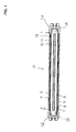
- Fig. 1 is a plan view of the female part of a thin, applied-to-surface type of electric connector according to a first embodiment of the present invention;
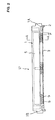
- Fig. 2 is a front view of the female part of the electric connector of the first embodiment of the present invention;
- Fig. 3 is a bottom view of the female part of the electric connector of the first embodiment of the present invention;
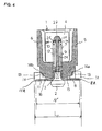
- Fig. 4 is a cross-section of the female part of the electric connector, taken along the line A-A in Fig. 2;
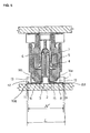
- Fig. 5 is a cross-section of the male and female parts of the electric connector when mated together;
- Fig. 6 is a perspective view of the female part of a thin, applied-to-surface type of electric connector according to a second embodiment of the present invention; and
- Fig. 7 is a cross-section of the female part of the electric connector of Fig. 6, taken along the line B-B in Fig. 6.
- Figs. 1 to 5 show the female part of a thin, applied-to-surface (surface mounted) type of electric connector according to a first embodiment of the present invention. It comprises a
housing 1 and a plurality ofterminals housing 1 hasposts 2 projecting downward from the opposite ends of itsbottom 3, as best seen from Fig. 2. Thehousing 1 has alongitudinal slot 4 formed in its top to receive the male part of the electric connector, which is attached to a counter printed circuit board. Thelongitudinal slot 4 runs between the front andrear sides housing 1. - An
elongate projection 23 extends into and lengthwise alongslot 4. The projection includes aportion 24 of theterminal receiving cavities 22 in opposite sides thereof. Eachportion 24 of the cavities within the projection ends in aslanted section 25 that slants away from the center of theprojection 23 downward towardsbottom 3 ofhousing 1. - Numerous terminals are arranged and fixed to the
housing body 1 in two parallel lines. Eachfront terminal 9 has acontact 7 and asoldering tail 8 at its opposite ends whereas eachrear terminal 12 has acontact 10 and asoldering tail 11 at its opposite ends. Thesesoldering tails rear sides tips 7A and 10A of the terminals adjacent thecontacts slanted section 25 of thehousing projection 23 so that thetips 7A and 10A cannot lift out of their respective cavity. - The structure described so far is similar to a conventional thin, surface mounted electric connector. The central feature of a thin, surface mounted electric connector according to the present invention is described below.
- As best seen in Figure 4, the distance N between the
tail end 8A of eachterminal 9 attached to thefront side 5 of thehousing 1 and thetail end 11 A of eachterminal 12 attached to therear side 6 of thehousing 1 is shorter than the maximum lateral size L of thehousing 1 thus remaining within the maximum lateral size L of thehousing 1. The lateral size or width of the housing is defined by the width between stabilizingprojections projections housing 1 lie. It can be seen that the width of the housing between the stabilizing projections is less than the width L at the stabilizing projections. - In addition, each of the front and
rear sides housing 1 has achamfer 13 along its lower longitudinal part or edge, thus permitting the bending of the tail end of each terminal. Specifically, thechamfer 13 is formed between the lower part of thefront side 5 and theplane 3 in which a printed circuit board is to be laid by partly removing the lower edge of thefront side 5 in a generallytriangular shape 13 to provide a steeplyslanted surface 15 and a more gentlyslanted surface 14a along the lower longitudinal part of thefront side 5. Likewise, thechamfer 13 is formed between the lower part of therear side 6 and theplane 3 by partly removing the lower edge of therear side 5 in the same manner to provide a steeplyslanted surface 16 and a more gentlyslanted surface 14b along the lower longitudinal part of therear side 5. These slanted surfaces of the bottom end of each opposite side facilitate the bending of thesolder tails - In use, a plurality of front and
rear terminals housing 1, and then these terminals are bent around the slanted surfaces of the bottom ends of the front andrear sides female part 17 of the electrical connector is placed on a printed circuit board with its front andrear terminal tails rear terminal tails terminal tails - Figs. 6 and 7 show a second embodiment of the present invention. As best seen from Fig. 7, the chamfer is formed by partly removing the lower edge of each of the front and
rear sides rectilinear recess 13 along the lower longitudinal part of each side. Thus, longitudinalrecessed walls rear sides housing 1. A plurality of front andrear terminals housing 1. There remain clearances between thesoldering tails rear terminals bottom ends rear sides housing 1 has no posts at its opposite ends to hold itself to a printed circuit board. - As may be understood from the above, the terminal tails are positioned within the maximum lateral size N of the connector housing, thus requiring no extra space in mounting the connector housing to a printed circuit board. Such a design still assures that the solder tails are exposed to a sufficient amount of heat to cause the melting of the solder applied thereon and to provide a good solder joint to each terminal.
Claims (7)
Applications Claiming Priority (2)
| Application Number | Priority Date | Filing Date | Title |
|---|---|---|---|
| JP32745/92U | 1992-04-18 | ||
| JP032745U JPH0584045U (en) | 1992-04-18 | 1992-04-18 | Thin surface mount electrical connector |
Publications (3)
| Publication Number | Publication Date |
|---|---|
| EP0567007A2 true EP0567007A2 (en) | 1993-10-27 |
| EP0567007A3 EP0567007A3 (en) | 1994-06-15 |
| EP0567007B1 EP0567007B1 (en) | 1996-08-21 |
Family
ID=12367384
Family Applications (1)
| Application Number | Title | Priority Date | Filing Date |
|---|---|---|---|
| EP93106205A Expired - Lifetime EP0567007B1 (en) | 1992-04-18 | 1993-04-16 | Electrical connector for surface mouting |
Country Status (7)
| Country | Link |
|---|---|
| US (1) | US5277597A (en) |
| EP (1) | EP0567007B1 (en) |
| JP (1) | JPH0584045U (en) |
| KR (1) | KR970002446B1 (en) |
| DE (1) | DE69304115T2 (en) |
| MY (1) | MY108951A (en) |
| SG (1) | SG43044A1 (en) |
Cited By (10)
| Publication number | Priority date | Publication date | Assignee | Title |
|---|---|---|---|---|
| EP0658951A1 (en) * | 1993-12-14 | 1995-06-21 | Molex Incorporated | Electrical connector for use in coupling two printed boards |
| EP0693804A3 (en) * | 1994-05-25 | 1996-10-30 | Molex Inc | Board to board connector |
| WO1997008780A1 (en) * | 1995-08-25 | 1997-03-06 | The Whitaker Corporation | Method for making surface mountable connectors |
| WO1997045896A1 (en) * | 1996-05-30 | 1997-12-04 | The Whitaker Corporation | Surface mountable electrical connector |
| EP0817324A2 (en) * | 1996-06-28 | 1998-01-07 | Berg Electronics Manufacturing B.V. | Electrical connector for use in miniaturized high density and high pin count applications and method of manufacture |
| US5772474A (en) * | 1995-09-07 | 1998-06-30 | Molex Incorporated | Electrical connector with embedded terminals |
| EP0881718A2 (en) * | 1997-05-30 | 1998-12-02 | Fujitsu Takamisawa Component Limited | High density connector |
| EP0907987A1 (en) * | 1996-06-28 | 1999-04-14 | Berg Technology, Inc. | Electrical connector |
| US6247970B1 (en) | 1998-08-24 | 2001-06-19 | Fujitsu Takamisawa Component Limited | Plug connector, jack connector and connector assembly |
| CN110676620A (en) * | 2018-07-03 | 2020-01-10 | 莫列斯有限公司 | Connector and connector assembly |
Families Citing this family (36)
| Publication number | Priority date | Publication date | Assignee | Title |
|---|---|---|---|---|
| JP3189480B2 (en) * | 1993-04-02 | 2001-07-16 | 富士電機株式会社 | Organic thin film light emitting device |
| JPH06291162A (en) * | 1993-04-02 | 1994-10-18 | Fuji Electric Co Ltd | Semiconductor integrated circuit chip |
| US5496180A (en) * | 1994-04-06 | 1996-03-05 | The Whitaker Corporation | Surface mountable card edge connector |
| US5525072A (en) * | 1995-01-10 | 1996-06-11 | Molex Incorporated | Electrical connector assembly for interconnecting a flat cable to a circuit board |
| US5713755A (en) * | 1995-09-11 | 1998-02-03 | Samtec, Inc. | Surface mount connectors having staked alignment pins |
| US5742481A (en) * | 1995-10-04 | 1998-04-21 | Advanced Interconnections Corporation | Removable terminal support member for integrated circuit socket/adapter assemblies |
| TW330739U (en) * | 1995-10-11 | 1998-04-21 | Hon Hai Prec Ind Co Ltd | Board-to-board connector assembly (I) |
| US5803752A (en) * | 1995-12-04 | 1998-09-08 | Hon Hai Precision Industry Co., Ltd. | Board-to-board connector |
| US5876217A (en) * | 1996-03-14 | 1999-03-02 | Molex Incorporated | Electric connector assembly with improved retention characteristics |
| US5873742A (en) * | 1996-06-18 | 1999-02-23 | Hon Hai Precision Ind. Co., Ltd. | Board-to-board connector assembly |
| US5885092A (en) * | 1996-06-21 | 1999-03-23 | Molex Incorporated | Electric connector assembly with improved registration characteristics |
| US6135781A (en) * | 1996-07-17 | 2000-10-24 | Minnesota Mining And Manufacturing Company | Electrical interconnection system and device |
| US5931705A (en) * | 1996-09-11 | 1999-08-03 | Thomas & Betts International | Surface mount wire connector |
| US6036504A (en) * | 1996-12-27 | 2000-03-14 | Hon Hai Precision Ind. Co., Ltd. | Board-to-board connector assembly |
| JPH10335000A (en) * | 1997-05-30 | 1998-12-18 | Molex Inc | Electrical connector assembly |
| US6048213A (en) * | 1998-02-11 | 2000-04-11 | Hon Hai Precision Ind. Co., Ltd. | Electrical connector assembly |
| USD429219S (en) * | 1998-07-23 | 2000-08-08 | Hon Hai Precision Ind. Co., Ltd. | Electrical connector |
| US6290547B2 (en) * | 1998-12-31 | 2001-09-18 | Berg Technologies, Inc. | Receptacle for an electrical connector |
| DE19939580C2 (en) * | 1999-08-20 | 2003-11-27 | Tyco Electronics Logistics Ag | Electrical connector |
| TW430188U (en) * | 1999-10-21 | 2001-04-11 | Hon Hai Prec Ind Co Ltd | Electrical connector |
| JP4381560B2 (en) * | 2000-04-13 | 2009-12-09 | 日本圧着端子製造株式会社 | Receptacle type connector and plug type connector |
| US6638106B1 (en) * | 2002-09-27 | 2003-10-28 | Hon Hai Precision Ind. Co., Ltd. | Multi-port electrical connector having improved board locks |
| JP2005190818A (en) * | 2003-12-25 | 2005-07-14 | Tyco Electronics Amp Kk | Electric connector and electric connector assembly |
| JP2005196975A (en) * | 2003-12-26 | 2005-07-21 | Jst Mfg Co Ltd | Connector |
| US7144277B2 (en) * | 2004-09-09 | 2006-12-05 | Hon Hai Precision Ind. Co., Ltd. | Electrical connector with guidance face |
| US7371129B2 (en) * | 2005-04-27 | 2008-05-13 | Samtec, Inc. | Elevated height electrical connector |
| US20070117268A1 (en) * | 2005-11-23 | 2007-05-24 | Baker Hughes, Inc. | Ball grid attachment |
| USD640637S1 (en) | 2009-01-16 | 2011-06-28 | Fci Americas Technology Llc | Vertical electrical connector |
| USD606497S1 (en) | 2009-01-16 | 2009-12-22 | Fci Americas Technology, Inc. | Vertical electrical connector |
| USD664096S1 (en) | 2009-01-16 | 2012-07-24 | Fci Americas Technology Llc | Vertical electrical connector |
| USD608293S1 (en) | 2009-01-16 | 2010-01-19 | Fci Americas Technology, Inc. | Vertical electrical connector |
| USD610548S1 (en) | 2009-01-16 | 2010-02-23 | Fci Americas Technology, Inc. | Right-angle electrical connector |
| CN201608386U (en) * | 2009-09-04 | 2010-10-13 | 富士康(昆山)电脑接插件有限公司 | Electric connector |
| JP5049361B2 (en) * | 2010-02-10 | 2012-10-17 | パナソニック株式会社 | Sockets and connectors |
| TWI479742B (en) * | 2012-05-11 | 2015-04-01 | Giga Byte Tech Co Ltd | Connector |
| JP7435366B2 (en) * | 2020-08-27 | 2024-02-21 | 住友電装株式会社 | board connector |
Citations (3)
| Publication number | Priority date | Publication date | Assignee | Title |
|---|---|---|---|---|
| FR2566590A1 (en) * | 1984-06-21 | 1985-12-27 | Oki Electric Ind Co Ltd | CONNECTOR FOR INTERCONNECTING PRINTED CIRCUIT BOARDS |
| US4795374A (en) * | 1987-05-04 | 1989-01-03 | Molex Incorporated | Double sided edge connector |
| EP0459680A2 (en) * | 1990-05-29 | 1991-12-04 | Molex Incorporated | Board-to-board electric connector having male and female terminals at reduced pitch |
Family Cites Families (5)
| Publication number | Priority date | Publication date | Assignee | Title |
|---|---|---|---|---|
| US4655518A (en) * | 1984-08-17 | 1987-04-07 | Teradyne, Inc. | Backplane connector |
| US4678250A (en) * | 1985-01-08 | 1987-07-07 | Methode Electronics, Inc. | Multi-pin electrical header |
| US4695106A (en) * | 1985-05-13 | 1987-09-22 | Amp Incorporated | Surface mount, miniature connector |
| JPH0638382Y2 (en) * | 1990-09-10 | 1994-10-05 | モレックス インコーポレーテッド | Surface mount connector for connecting boards |
| US5161985A (en) * | 1991-08-08 | 1992-11-10 | Robinson Nugent, Inc. | Board to board interconnect |
-
1992
- 1992-04-18 JP JP032745U patent/JPH0584045U/en active Pending
-
1993
- 1993-03-10 US US08/029,197 patent/US5277597A/en not_active Expired - Lifetime
- 1993-03-19 MY MYPI93000483A patent/MY108951A/en unknown
- 1993-04-16 SG SG1996002962A patent/SG43044A1/en unknown
- 1993-04-16 EP EP93106205A patent/EP0567007B1/en not_active Expired - Lifetime
- 1993-04-16 DE DE69304115T patent/DE69304115T2/en not_active Expired - Fee Related
- 1993-04-17 KR KR1019930006506A patent/KR970002446B1/en not_active IP Right Cessation
Patent Citations (3)
| Publication number | Priority date | Publication date | Assignee | Title |
|---|---|---|---|---|
| FR2566590A1 (en) * | 1984-06-21 | 1985-12-27 | Oki Electric Ind Co Ltd | CONNECTOR FOR INTERCONNECTING PRINTED CIRCUIT BOARDS |
| US4795374A (en) * | 1987-05-04 | 1989-01-03 | Molex Incorporated | Double sided edge connector |
| EP0459680A2 (en) * | 1990-05-29 | 1991-12-04 | Molex Incorporated | Board-to-board electric connector having male and female terminals at reduced pitch |
Cited By (25)
| Publication number | Priority date | Publication date | Assignee | Title |
|---|---|---|---|---|
| US5639248A (en) * | 1993-12-14 | 1997-06-17 | Molex Incorporated | Electric connector assembly for use in couplings two printed boards |
| US5641290A (en) * | 1993-12-14 | 1997-06-24 | Molex Incorporated | Electric connector assembly for use in coupling two printed boards |
| EP0658951A1 (en) * | 1993-12-14 | 1995-06-21 | Molex Incorporated | Electrical connector for use in coupling two printed boards |
| EP0693804A3 (en) * | 1994-05-25 | 1996-10-30 | Molex Inc | Board to board connector |
| WO1997008780A1 (en) * | 1995-08-25 | 1997-03-06 | The Whitaker Corporation | Method for making surface mountable connectors |
| US5772474A (en) * | 1995-09-07 | 1998-06-30 | Molex Incorporated | Electrical connector with embedded terminals |
| WO1997045896A1 (en) * | 1996-05-30 | 1997-12-04 | The Whitaker Corporation | Surface mountable electrical connector |
| US6048482A (en) * | 1996-06-28 | 2000-04-11 | Berg Technology, Inc. | Method for manufacturing an electrical connector |
| US6065951A (en) * | 1996-06-28 | 2000-05-23 | Berg Technology, Inc. | Mold for use in manufacturing an electrical connector |
| EP0907987A1 (en) * | 1996-06-28 | 1999-04-14 | Berg Technology, Inc. | Electrical connector |
| EP0907987A4 (en) * | 1996-06-28 | 2000-08-09 | Berg Tech Inc | Electrical connector |
| EP0817324A3 (en) * | 1996-06-28 | 1999-10-20 | Berg Electronics Manufacturing B.V. | Electrical connector for use in miniaturized high density and high pin count applications and method of manufacture |
| EP0817324A2 (en) * | 1996-06-28 | 1998-01-07 | Berg Electronics Manufacturing B.V. | Electrical connector for use in miniaturized high density and high pin count applications and method of manufacture |
| EP2273628A1 (en) * | 1997-05-30 | 2011-01-12 | Fujitsu Component Limited | High density connector |
| EP0881718A3 (en) * | 1997-05-30 | 1999-08-11 | Fujitsu Takamisawa Component Limited | High density connector |
| US6439928B1 (en) | 1997-05-30 | 2002-08-27 | Fujitsu Takamisawa Component Limited | High density connector for balanced transmission lines |
| US6533614B1 (en) | 1997-05-30 | 2003-03-18 | Fujitsu Takamisawa Component Limited | High density connector for balanced transmission lines |
| US6805586B2 (en) | 1997-05-30 | 2004-10-19 | Fujitsu Takamisawa Component Limited | High density connector for balanced transmission lines |
| EP0881718A2 (en) * | 1997-05-30 | 1998-12-02 | Fujitsu Takamisawa Component Limited | High density connector |
| EP2290761A1 (en) * | 1997-05-30 | 2011-03-02 | Fujitsu Component Limited | High density connector |
| US6247970B1 (en) | 1998-08-24 | 2001-06-19 | Fujitsu Takamisawa Component Limited | Plug connector, jack connector and connector assembly |
| US6368121B1 (en) | 1998-08-24 | 2002-04-09 | Fujitsu Takamisawa Component Limited | Plug connector, jack connector and connector assembly |
| CN110676620A (en) * | 2018-07-03 | 2020-01-10 | 莫列斯有限公司 | Connector and connector assembly |
| CN110676620B (en) * | 2018-07-03 | 2021-08-20 | 莫列斯有限公司 | Connector and connector assembly |
| US11509094B2 (en) | 2018-07-03 | 2022-11-22 | Molex, Llc | Connector and connector assembly |
Also Published As
| Publication number | Publication date |
|---|---|
| EP0567007B1 (en) | 1996-08-21 |
| KR930022635A (en) | 1993-11-24 |
| EP0567007A3 (en) | 1994-06-15 |
| DE69304115T2 (en) | 1997-01-16 |
| JPH0584045U (en) | 1993-11-12 |
| US5277597A (en) | 1994-01-11 |
| MY108951A (en) | 1996-11-30 |
| KR970002446B1 (en) | 1997-03-05 |
| SG43044A1 (en) | 1997-10-17 |
| DE69304115D1 (en) | 1996-09-26 |
Similar Documents
| Publication | Publication Date | Title |
|---|---|---|
| US5277597A (en) | Thin, applied-to-surface type of electric connector | |
| EP0569893B1 (en) | Low profile electrical connector | |
| KR100236435B1 (en) | Electric connector with improved terminal-receiving passage means | |
| US5498167A (en) | Board to board electrical connectors | |
| US4708415A (en) | Electrical connectors | |
| EP0543278B1 (en) | Low profile electrical connector | |
| EP0459680B1 (en) | Board-to-board electric connector having male and female terminals at reduced pitch | |
| EP0969570A1 (en) | Connector shield termination | |
| EP0555963A1 (en) | Connector with one piece ground bus | |
| EP0724313A2 (en) | Printed circuit board mounted electrical connector | |
| US5695354A (en) | Printed circuit board connector | |
| US5919051A (en) | Flat back card connector | |
| EP0448382A1 (en) | Improved female terminal for an electrical connector | |
| EP0774808B1 (en) | Right-angle board to board connector with anti-wicking characteristics and terminal for same | |
| US4708416A (en) | Electrical connecting terminal for a connector | |
| EP0487866A2 (en) | Electrical connector assembly for mounting on a printed circuit board | |
| US5378175A (en) | Electrical connector for mounting on a printed circuit board | |
| US20010014548A1 (en) | Electrical connector | |
| EP0932226A2 (en) | Card connector | |
| JP3082088B2 (en) | Terminal holding mechanism | |
| US6109981A (en) | Socket contact | |
| US6338633B1 (en) | Electrical connector with improved contacts | |
| EP0702425B1 (en) | Improved solder tail and electric connector incorporating same | |
| US4681391A (en) | Electric connector | |
| EP0762559A2 (en) | Electric connector terminal having a round soldering tail |
Legal Events
| Date | Code | Title | Description |
|---|---|---|---|
| PUAI | Public reference made under article 153(3) epc to a published international application that has entered the european phase |
Free format text: ORIGINAL CODE: 0009012 |
|
| AK | Designated contracting states |
Kind code of ref document: A2 Designated state(s): DE ES FR GB IT NL |
|
| RIN1 | Information on inventor provided before grant (corrected) |
Inventor name: MIYAZAWA, JUNICHI Inventor name: SASAO, MASAMI |
|
| PUAL | Search report despatched |
Free format text: ORIGINAL CODE: 0009013 |
|
| AK | Designated contracting states |
Kind code of ref document: A3 Designated state(s): DE ES FR GB IT NL |
|
| 17P | Request for examination filed |
Effective date: 19941201 |
|
| 17Q | First examination report despatched |
Effective date: 19950510 |
|
| GRAG | Despatch of communication of intention to grant |
Free format text: ORIGINAL CODE: EPIDOS AGRA |
|
| GRAH | Despatch of communication of intention to grant a patent |
Free format text: ORIGINAL CODE: EPIDOS IGRA |
|
| GRAH | Despatch of communication of intention to grant a patent |
Free format text: ORIGINAL CODE: EPIDOS IGRA |
|
| ITF | It: translation for a ep patent filed |
Owner name: DE DOMINICIS & MAYER S.R.L. |
|
| GRAA | (expected) grant |
Free format text: ORIGINAL CODE: 0009210 |
|
| AK | Designated contracting states |
Kind code of ref document: B1 Designated state(s): DE ES FR GB IT NL |
|
| REF | Corresponds to: |
Ref document number: 69304115 Country of ref document: DE Date of ref document: 19960926 |
|
| ET | Fr: translation filed | ||
| PG25 | Lapsed in a contracting state [announced via postgrant information from national office to epo] |
Ref country code: ES Free format text: LAPSE BECAUSE OF FAILURE TO SUBMIT A TRANSLATION OF THE DESCRIPTION OR TO PAY THE FEE WITHIN THE PRESCRIBED TIME-LIMIT Effective date: 19961202 |
|
| PGFP | Annual fee paid to national office [announced via postgrant information from national office to epo] |
Ref country code: ES Payment date: 19970424 Year of fee payment: 5 |
|
| PLBE | No opposition filed within time limit |
Free format text: ORIGINAL CODE: 0009261 |
|
| STAA | Information on the status of an ep patent application or granted ep patent |
Free format text: STATUS: NO OPPOSITION FILED WITHIN TIME LIMIT |
|
| 26N | No opposition filed | ||
| PGFP | Annual fee paid to national office [announced via postgrant information from national office to epo] |
Ref country code: GB Payment date: 20010313 Year of fee payment: 9 |
|
| PGFP | Annual fee paid to national office [announced via postgrant information from national office to epo] |
Ref country code: NL Payment date: 20010319 Year of fee payment: 9 |
|
| REG | Reference to a national code |
Ref country code: GB Ref legal event code: IF02 |
|
| PGFP | Annual fee paid to national office [announced via postgrant information from national office to epo] |
Ref country code: FR Payment date: 20020404 Year of fee payment: 10 |
|
| PG25 | Lapsed in a contracting state [announced via postgrant information from national office to epo] |
Ref country code: GB Free format text: LAPSE BECAUSE OF NON-PAYMENT OF DUE FEES Effective date: 20020416 |
|
| PGFP | Annual fee paid to national office [announced via postgrant information from national office to epo] |
Ref country code: DE Payment date: 20020430 Year of fee payment: 10 |
|
| PG25 | Lapsed in a contracting state [announced via postgrant information from national office to epo] |
Ref country code: NL Free format text: LAPSE BECAUSE OF NON-PAYMENT OF DUE FEES Effective date: 20021101 |
|
| GBPC | Gb: european patent ceased through non-payment of renewal fee |
Effective date: 20020416 |
|
| NLV4 | Nl: lapsed or anulled due to non-payment of the annual fee |
Effective date: 20021101 |
|
| PG25 | Lapsed in a contracting state [announced via postgrant information from national office to epo] |
Ref country code: DE Free format text: LAPSE BECAUSE OF NON-PAYMENT OF DUE FEES Effective date: 20031101 |
|
| PG25 | Lapsed in a contracting state [announced via postgrant information from national office to epo] |
Ref country code: FR Free format text: LAPSE BECAUSE OF NON-PAYMENT OF DUE FEES Effective date: 20031231 |
|
| REG | Reference to a national code |
Ref country code: FR Ref legal event code: ST |
|
| PG25 | Lapsed in a contracting state [announced via postgrant information from national office to epo] |
Ref country code: IT Free format text: LAPSE BECAUSE OF NON-PAYMENT OF DUE FEES;WARNING: LAPSES OF ITALIAN PATENTS WITH EFFECTIVE DATE BEFORE 2007 MAY HAVE OCCURRED AT ANY TIME BEFORE 2007. THE CORRECT EFFECTIVE DATE MAY BE DIFFERENT FROM THE ONE RECORDED. Effective date: 20050416 |