EP0569090A1 - Image sensor - Google Patents
Image sensor Download PDFInfo
- Publication number
- EP0569090A1 EP0569090A1 EP93201253A EP93201253A EP0569090A1 EP 0569090 A1 EP0569090 A1 EP 0569090A1 EP 93201253 A EP93201253 A EP 93201253A EP 93201253 A EP93201253 A EP 93201253A EP 0569090 A1 EP0569090 A1 EP 0569090A1
- Authority
- EP
- European Patent Office
- Prior art keywords
- photosensitive
- image sensor
- switching
- elements
- conductors
- Prior art date
- Legal status (The legal status is an assumption and is not a legal conclusion. Google has not performed a legal analysis and makes no representation as to the accuracy of the status listed.)
- Granted
Links
- 239000004020 conductor Substances 0.000 claims abstract description 102
- 239000003990 capacitor Substances 0.000 claims abstract description 47
- 239000000758 substrate Substances 0.000 claims abstract description 26
- 239000011159 matrix material Substances 0.000 claims description 13
- 239000003086 colorant Substances 0.000 claims description 8
- 238000005286 illumination Methods 0.000 claims description 7
- 238000000034 method Methods 0.000 claims description 6
- 239000002131 composite material Substances 0.000 claims description 4
- 230000005669 field effect Effects 0.000 claims description 4
- 230000003213 activating effect Effects 0.000 claims description 2
- 230000035945 sensitivity Effects 0.000 abstract description 2
- 239000010410 layer Substances 0.000 description 26
- 239000004973 liquid crystal related substance Substances 0.000 description 18
- 239000000463 material Substances 0.000 description 12
- 239000011295 pitch Substances 0.000 description 7
- VYPSYNLAJGMNEJ-UHFFFAOYSA-N Silicium dioxide Chemical compound O=[Si]=O VYPSYNLAJGMNEJ-UHFFFAOYSA-N 0.000 description 6
- AMGQUBHHOARCQH-UHFFFAOYSA-N indium;oxotin Chemical compound [In].[Sn]=O AMGQUBHHOARCQH-UHFFFAOYSA-N 0.000 description 6
- VYZAMTAEIAYCRO-UHFFFAOYSA-N Chromium Chemical compound [Cr] VYZAMTAEIAYCRO-UHFFFAOYSA-N 0.000 description 4
- 229910052581 Si3N4 Inorganic materials 0.000 description 4
- 238000012986 modification Methods 0.000 description 4
- 230000004048 modification Effects 0.000 description 4
- 238000000059 patterning Methods 0.000 description 4
- 238000012545 processing Methods 0.000 description 4
- HQVNEWCFYHHQES-UHFFFAOYSA-N silicon nitride Chemical compound N12[Si]34N5[Si]62N3[Si]51N64 HQVNEWCFYHHQES-UHFFFAOYSA-N 0.000 description 4
- 229910021417 amorphous silicon Inorganic materials 0.000 description 3
- 229910052804 chromium Inorganic materials 0.000 description 3
- 239000011651 chromium Substances 0.000 description 3
- 238000000151 deposition Methods 0.000 description 3
- 230000001681 protective effect Effects 0.000 description 3
- 239000004065 semiconductor Substances 0.000 description 3
- 239000010409 thin film Substances 0.000 description 3
- 239000004642 Polyimide Substances 0.000 description 2
- 230000000295 complement effect Effects 0.000 description 2
- 238000001514 detection method Methods 0.000 description 2
- 230000005670 electromagnetic radiation Effects 0.000 description 2
- 239000011521 glass Substances 0.000 description 2
- 238000003384 imaging method Methods 0.000 description 2
- 230000002452 interceptive effect Effects 0.000 description 2
- 238000001465 metallisation Methods 0.000 description 2
- 239000004033 plastic Substances 0.000 description 2
- 229920003023 plastic Polymers 0.000 description 2
- 229920001721 polyimide Polymers 0.000 description 2
- 235000012239 silicon dioxide Nutrition 0.000 description 2
- 239000000377 silicon dioxide Substances 0.000 description 2
- 229910052814 silicon oxide Inorganic materials 0.000 description 2
- 239000004988 Nematic liquid crystal Substances 0.000 description 1
- 206010034972 Photosensitivity reaction Diseases 0.000 description 1
- 239000000853 adhesive Substances 0.000 description 1
- 230000001070 adhesive effect Effects 0.000 description 1
- 229910052782 aluminium Inorganic materials 0.000 description 1
- XAGFODPZIPBFFR-UHFFFAOYSA-N aluminium Chemical compound [Al] XAGFODPZIPBFFR-UHFFFAOYSA-N 0.000 description 1
- 239000004411 aluminium Substances 0.000 description 1
- 230000015572 biosynthetic process Effects 0.000 description 1
- 230000007547 defect Effects 0.000 description 1
- 230000001419 dependent effect Effects 0.000 description 1
- 239000003822 epoxy resin Substances 0.000 description 1
- 238000010348 incorporation Methods 0.000 description 1
- 238000003780 insertion Methods 0.000 description 1
- 230000037431 insertion Effects 0.000 description 1
- 239000011810 insulating material Substances 0.000 description 1
- 238000012015 optical character recognition Methods 0.000 description 1
- 230000036211 photosensitivity Effects 0.000 description 1
- 229910021420 polycrystalline silicon Inorganic materials 0.000 description 1
- 229920000647 polyepoxide Polymers 0.000 description 1
- 239000002861 polymer material Substances 0.000 description 1
- 239000011241 protective layer Substances 0.000 description 1
- 238000000926 separation method Methods 0.000 description 1
- 238000012546 transfer Methods 0.000 description 1
- 230000000007 visual effect Effects 0.000 description 1
Images


Classifications
-
- H—ELECTRICITY
- H01—ELECTRIC ELEMENTS
- H01L—SEMICONDUCTOR DEVICES NOT COVERED BY CLASS H10
- H01L27/00—Devices consisting of a plurality of semiconductor or other solid-state components formed in or on a common substrate
- H01L27/14—Devices consisting of a plurality of semiconductor or other solid-state components formed in or on a common substrate including semiconductor components sensitive to infrared radiation, light, electromagnetic radiation of shorter wavelength or corpuscular radiation and specially adapted either for the conversion of the energy of such radiation into electrical energy or for the control of electrical energy by such radiation
- H01L27/144—Devices controlled by radiation
- H01L27/146—Imager structures
- H01L27/14601—Structural or functional details thereof
- H01L27/14609—Pixel-elements with integrated switching, control, storage or amplification elements
-
- H—ELECTRICITY
- H01—ELECTRIC ELEMENTS
- H01L—SEMICONDUCTOR DEVICES NOT COVERED BY CLASS H10
- H01L27/00—Devices consisting of a plurality of semiconductor or other solid-state components formed in or on a common substrate
- H01L27/02—Devices consisting of a plurality of semiconductor or other solid-state components formed in or on a common substrate including semiconductor components specially adapted for rectifying, oscillating, amplifying or switching and having at least one potential-jump barrier or surface barrier; including integrated passive circuit elements with at least one potential-jump barrier or surface barrier
- H01L27/12—Devices consisting of a plurality of semiconductor or other solid-state components formed in or on a common substrate including semiconductor components specially adapted for rectifying, oscillating, amplifying or switching and having at least one potential-jump barrier or surface barrier; including integrated passive circuit elements with at least one potential-jump barrier or surface barrier the substrate being other than a semiconductor body, e.g. an insulating body
-
- H—ELECTRICITY
- H01—ELECTRIC ELEMENTS
- H01L—SEMICONDUCTOR DEVICES NOT COVERED BY CLASS H10
- H01L27/00—Devices consisting of a plurality of semiconductor or other solid-state components formed in or on a common substrate
- H01L27/14—Devices consisting of a plurality of semiconductor or other solid-state components formed in or on a common substrate including semiconductor components sensitive to infrared radiation, light, electromagnetic radiation of shorter wavelength or corpuscular radiation and specially adapted either for the conversion of the energy of such radiation into electrical energy or for the control of electrical energy by such radiation
- H01L27/144—Devices controlled by radiation
- H01L27/146—Imager structures
- H01L27/14643—Photodiode arrays; MOS imagers
Definitions
- This invention relates to an image sensor comprising a transparent substrate supporting a two dimensional array of photosensitive and switching elements and switching signal conductors and data signal conductors connected to the photosensitive and switching elements for enabling individual photosensitive elements to be accessed, the photosensitive and switching elements and conductors being arranged such that at least half of the area of the image sensor is transparent during operation.
- Such an image sensor is described in EP-A-378593 (International Publication No. WO 89/09960).
- the image sensor described in that document has a matrix array of photosensitive diodes connected back to back with switching diodes between row and column conductors. Each photosensitive diode may be formed on top of the associated switching diode.
- the image sensor is designed to be placed on top of, for example, an electro-optic display which requires the image sensor to be sufficiently transparent that the image produced by the display is still identifiable when viewed through the image sensor.
- the photosensitive diodes are designed to occupy equal to or less than 50% of the surface area of the image sensor.
- the light collection efficiency of the photosensitive diodes reduces with area. It is accordingly necessary to accept a compromise between the dynamic range (that is the detection limit or number of gray scale levels which can be detected under a given illumination level) of the image sensor and the degree of obscuration of the display device.
- an image sensor comprising a transparent substrate supporting a two dimensional array of photosensitive and switching elements with switching signal conductors and data signal conductors connected to the photosensitive and switching elements for enabling individual photosensitive elements to be accessed, the photosensitive and switching elements and conductors being arranged such that at least half of the area of the image sensor is transparent during operation, characterised in that each photosensitive element is electrically coupled to a respective capacitor for storing charge generated as a result of light being incident on the photosensitive element, the capacitors being formed so as to be transparent and so as to occupy a significant part of the entire area of the array.
- the term 'light' normal means electromagnetic radiation visible to the human eye but could be applied, by the use of appropriate materials to form the photosensitive elements, to electromagnetic radiation in, for example, the near infra-red and the term 'transparent' means that the material concerned absorbs very little, for example less than about 20%, of the light incident thereon.
- the transparent capacitors act effectively to increase the dynamic range of the photosensitive elements by enabling a high quantity of charge to be stored in response to light incident on the photosensitive elements.
- the light capturing area of the photosensitive elements can therefore be quite small while still providing sufficient signal to enable high accuracy in the sensing of an image.
- the array may be, for example, up to about 90% transparent enabling it to be provided over, probably in contact with, a display device (which may be a cathode ray tube or other form of electro-optic display device such as a liquid crystal display device) without the image sensor unduly interfering with the image projected by the display device during its normal use.
- the photosensitive elements may be shielded from the transparent substrate by the switching signal conductors.
- the photosensitive elements may be provided on top of the opaque switching signal conductors which reduces the area of the image sensor occupied by non-transparent components while shielding the photosensitive elements from light directed at the substrate for example from an electro-optic display on which the image sensor is mounted.
- Two or more photosensitive elements may be associated with the same pair of switching signal and data signal conductors and arranged to have different switching signal thresholds, for example by being associated with switching elements with different switching thresholds, so that the two or more photosensitive elements can be accessed separately by applying different threshold switching signals to the switching signal conductor.
- the present invention provides an image sensor comprising a transparent substrate supporting a two dimensional array of photosensitive and switching elements and switching signal conductors and data signal conductors connected to the photosensitive and switching elements for enabling individual photosensitive elements to be accessed, the photosensitive and switching elements and conductors being arranged such that a substantial part for example at least about half, of the area of the image sensor is transparent, the switching signal conductors being opaque and the photosensitive and switching elements being provided on the switching signal conductors so as to be shielded from the transparent substrate characterised in that two or more photosensitive elements are associated with the same pair of switching signal and data signal conductors and are arranged to have different switching signal thresholds so that the two or more photosensitive elements can be accessed separately by applying different threshold switching signals to the switching signal conductor.
- the image sensor is to be provided on top of an active matrix-addressed electro-optic display this should enable the image sensor to have the same number of switching signal and data conductors as the display, so allowing the switching signal and data conductors of the image sensor to be aligned with the corresponding conductors of the display device and in particular with any mask used to shield the display switching elements from incident light. This should allow minimum, if any,obscuration of the display image by the image sensor while allowing the image sensor to have a higher resolution than the display. This should enable the image sensor to be able to sense or read text and should allow for optical character recognition with appropriate circuitry and software.
- Each switching element may comprise a diode or a number of series-connected diodes.
- each switching element may comprise an insulated gate field effect transistor and the transistors associated with different ones of the two or more photosensitive elements may have different threshold voltages by, for example, providing a respective voltage-adjusting element between the gate electrode of the transistor and the switching signal conductor.
- the present invention also provides a method of forming a colour image sensor which method comprises providing an image sensor in accordance with the first aspect of the invention on a colour display device, for example a liquid crystal display device, activating the colour display device so as to illuminate an image being sensed by the image sensor sequentially with three different colours of light, reading out sets of signals from the image sensor representing the image as sensed under each different colour illumination and combining the three sets of signals to produce a set of composite signals representing the full colour image.
- a colour display device for example a liquid crystal display device
- any suitable three 'colours' of light may be used for example the three primary (red, green and blue) or the three complementary (cyan, magenta and yellow) may be used.
- one of the colours of light may be white light and the other two may be any selected two of the complementary colours).
- the image sensor 1a,1b,1c or 1d comprises a transparent substrate 2 supporting a two dimensional array 3 of photosensitive and switching elements 4 with switching signal conductors 5 and data signal conductors 6 connected to the photosensitive and switching elements 4 for enabling individual photosensitive elements to be accessed, the photosensitive and switching elements 4 and the conductors 5 and 6 being arranged such that at least half of the area of the image sensor is transparent during operation.
- each photosensitive element is electrically coupled to a respective capacitor 7 for storing charge generated as a result of light being incident on the photosensitive element, the capacitors 7 being formed so as to be transparent and so as to occupy a significant part of the entire area of the array 3, where the term 'significant part' should be understood to mean at least 10% and preferably 50% or more of the area not occupied by the switching signal and data signal conductors 5 and 6.
- the transparent capacitors act effectively to increase the sensitivity of the photosensitive elements by enabling a high quantity of charge to be stored in response to light incident on the photosensitive elements.
- the array may be, for example, up to about 90% transparent enabling it to be provided over, probably in contact with, a display device which may be a cathode ray tube or other form of electrooptic display device such as a liquid crystal display device, without the image sensor unduly interfering with the image projected by the display device during its normal use.
- Such an image sensor may be used, for example, to enable a contact image to be obtained merely by placing the document to be imaged onto the top of the combined display and image sensor. The image of the document may then be displayed by use of conventional electronic and video circuitry to transfer the stored image directly to the display device.
- the image sensor may be used to enable a light pen or similar device to be used to 'write' onto the display of a conventional cathode ray tube or liquid crystal display device.
- Figure 1 is a schematic circuit layout of one example of an image sensor 1a in accordance with the invention.
- the array 3 may have an overall size of up to 400 by 400mm with a pitch between adjacent photosensitive and switching elements of about 200 ⁇ m.
- Each photosensitive element may be a diode, generally a p-i-n diode, which may also form the switching element. This diode is given the reference numeral 4 in Figure 1.
- each photosensitive and switching element 4a is connected in series with the capacitor 7 between a switching signal or row conductor 5 and a data signal or column conductor 6 so that each photosensitive and switching element 4a is associated with a unique pairing of row and column conductors 5 and 6 enabling each photosensitive element 4 to be accessed individually.
- the row and column conductors 5 and 6 are arranged in a matrix of 1-m rows and 1-n columns (only three rows and columns being shown).
- the row conductors 5 are connected to a row driver or decoder/addressing circuit 8 while the column conductors 6 are connected including a charge-sensitive read-out amplifier arrangement 9 which may be of conventional type.
- a read-out arrangement of the type described in EP-A-440282 could also be used.
- the matrix array of row and column conductors 5 and 6 defines a grid of image areas 10 each of which is bounded by two adjacent pairs of intersecting row and column conductors 5 and 6.
- each image area 10 is associated with a single photosensitive and switching element 4a.
- each photosensitive and switching element 4a is reverse-biassed by appropriate switching signals on the row conductors 5 in order to enable sensing of an image so as to allow charge to be stored on the associated capacitor 7.
- Each photosensitive and switching element 4a may then be forward-biassed in succession to enable the charge stored in the associated capacitor 7 to be read-out.
- Systems for addressing individual photosensitive elements and reading the charge (data) stored thereat are well known to the image sensing art (see for example EP-A-233104, EP-A-234968) and have derived, for example, from the active matrix addressing systems used for electro-optic, in particular LCD, displays. Accordingly, the details of the addressing and reading systems will not be given.
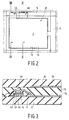
- Figure 2 illustrates very schematically a plan view of the top conductive levels of an image area 10 of the image sensor 1a together with at least parts of the row and column conductors 5 and 6 bounding the image area.
- the area of the photosensitive and switch element is indicated by the appropriate reference numeral in Figure 3 which is a cross-section along the line III-III of the image area 10 shown in Figure 2.
- the transparent substrate 2 is formed of glass, although other materials even flexible materials such as suitable plastics materials could be used.
- the image sensor 1a is formed upon the transparent substrate 2 using conventional thin film processing techniques.
- the row conductors 5 are first formed by depositing and patterning a layer of a suitable opaque electrically conductive material, in this example chrome.
- the photosensitive and switching elements 4a are then formed as, preferably, n-i-p (with the p conductivity layer adjacent the chromium row conductors 5) diodes, although p-i-n diodes could be used, by depositing and then patterning appropriately doped layers 40,41 and 42 of, in this example, amorphous silicon.
- An insulating layer 11, for example of silicon oxide or silicon nitride is then deposited and patterned to form a window to enable contact to be made to the diodes 4a.
- a layer of a transparent electrically conductive material is then deposited and patterned to define the top contacts 12 to the diodes 4.
- the top contact 12 of each diode 4 is formed integrally with the bottom transparent electrode 7a of the associated capacitor 7.
- a layer 13 of a transparent insulating material, such as silicon oxide or silicon nitride, is then deposited to form the capacitor dielectric followed by a layer of a transparent electrically conductive material, again generally indium tin oxide, which is patterned to define the top electrodes 7b of the capacitors 7 and the column conductors 6.
- the conductivity of the column conductors 6 may, if necessary, be increased by depositing and patterning, for example, an aluminium layer so as to provide a composite structure for the column electrodes 6.
- the completed structure is generally be covered by a protective transparent insulating layer 14 such as a layer of polyimide.
- the transparent capacitors 7 occupy a significant part of the image areas 10.
- the capacitors may have a capacitance in the range of from about 0.1 to about 5pF (picofarads).
- the actual proportion of each image area 10 occupied by the capacitor 7 will generally be most dependent on the pixel pitch (that is the distance between the centres of adjacent image areas 10) because it is likely that similar capacitances will be required even if the pixel pitches are different.
- the capacitor 7 might occupy between 50% and 100% of the area 10 not occupied by the conductors 5 and 6, while where the pixel pitch is about 0.2mm then the part of the area 10 occupied by the capacitors 7 may fall to 10% to 20% for a similar capacitance although, of course, larger capacitances could be used.
- the use of extremely large area, may be advantageous in further increasing the dynamic range, even materials such as indium tin oxide (ITO) absorb a small amount of light and thus reduce the transparency of the device.
- ITO indium tin oxide
- the photosensitive and switching elements 4a are provided on top of the opaque row conductors 5 which has the advantages of automatically shielding the photosensitive and switching elements 4a from light transmitted through the substrate 2 towards the photosensitive and switching elements 4a and in addition means that the photosensitive element (which of course must absorb the light to be sensed and cannot therefore be transparent) is provided on an area of the image sensor 1a which is already opaque. Accordingly, the amount of the image sensor 1a area which is opaque need not in any way affected by the presence of the photosensitive and switching elements 4a. Typically, as much as 90% of the entire area of the image sensor 1a may be transparent.
- Figure 4 is a circuit layout of one image area 10 for illustrating a modification of the circuit shown in Figure 1 which enables an even greater proportion of the area of the image sensor to be transparent.
- threshold adjusting devices 14 are provided so that a different level of switching signal is required on the row conductor 5 to access different ones of the photosensitive elements associated with the same pair of row and column conductors 5 and 6.
- the threshold adjusting devices 14 are in the form of additional diodes connected in series with the diodes forming the photosensitive and switching elements 4a.
- three photosensitive and switching element diodes 4a are associated with the same pair of row and column conductors 5 and 6, although as indicated by the broken lines, more (or fewer) photosensitive and switching elements 5 and 6 could be associated with each image area 10.
- the number of series-connected additional diodes 14 used to adjust the threshold voltage at which a given photosensitive diode 4a can be accessed will of course depend on the characteristics of the threshold adjusting diodes 14 and the switching signal voltage levels which are available.
- the threshold adjusting diodes 14 may be formed on the opaque row conductors 5 in a similar manner to the photosensitive diodes 4a.
- the threshold adjusting diodes 14 need of course to be shielded from the light to be detected by the photosensitive diodes 4a. This may be achieved by forming the respective photosensitive diode 4 on top of the associated threshold adjusting diode or diode stack 14 or by providing an opaque (generally chromium) top contact for the threshold adjusting diodes 14.
- the separate capacitors 7', 7'' and 7''' in the example shown in Figure 4 may be formed quite simply by patterning of the indium tin oxide layers in appropriate manner to define, in this case, three discrete capacitors of any desired geometry in each image area 10.
- the separate capacitors 7', 7'' and 7''' may all be of the same or similar size so that each provides a similar value signal, thereby simplifying processing.
- the separate capacitors 7', 7'' and 7''' may have significantly different areas (and thus capacitances) which may facilitate identification of the particular capacitor supplying a signal, at the expense of further processing circuitry.
- the capacitor 7' may be smaller than the capacitor 7'' which may in turn be smaller than the capacitor 7'''. This may assist in ensuring that, when its signal is readout, each capacitor is fully discharged before the signal is read from the next higher threshold subsidiary pixel.
- An image sensor 1b having image areas 10 with the structure shown in Figure 4 has the additional advantage that, as a unique pair of row and column conductors 5 and 6 is not necessary for each photosensitive and switching element the same degree of image resolution (pixel pitch) can be achieved with less, or more widely separated, row and column conductors 5 and 6, thereby reducing the amount of the area of the image sensor 1b taken up by the opaque conductors 5 and 6 and so allowing a larger area of the image sensor 1b to be transparent.
- the photosensitive and switching elements are provided by a single photosensitive diode 4a.
- the photosensitive elements may be separated from the switching elements.
- the photosensitive elements do not need to have a switching capability and could be for example photosensitive resistors.
- FIGs 1 and 4 illustrate in phantom lines the use of a separate photosensitive element 4b.
- the photosensitive element is a photosensitive diode 4b arranged in parallel with the associated capacitor 7.
- This photosensitive diode 4b is indicated by dashed lines in Figure 4.
- Figure 5 illustrates a possible structure for such a photosensitive diode 4b.
- the photosensitive diode 4b has a similar structure to that shown in Figure 3 for the combined photosensitive and switching diode 4a except that, of course, the photosensitive diode 4b is electrically isolated from the opaque row conductor 5 by an insulating layer 15 and the indium tin oxide layers providing the bottom and top electrodes 7a and 7b of the capacitor 7 are patterned so as to define the bottom and top electrodes 4'b and 4''b, respectively, of the photosensitive diode 4b.
- the other diode labelled 4a in Figures 1 and 4 is not intended to be photosensitive and should be shielded from the light incident on the image sensor in a manner similar to that described above in relation to the threshold adjusting diodes 14.
- switching element and threshold adjusting diodes 4a and 14 have been described above as being p-i-n diodes, other types of diodes, for example thin-film Schottky diodes or other non-linear switching elements such as MIM devices may be used. Where such devices can be made to have sufficient photosensitivity they could also be used as the photosensitive elements, either as the separate photosensitive elements 4b (shown in dashed lines in Figures 1 and 4) or as the combined photosensitive and switching elements 4a described above.
- the photosensitive and switching elements may be formed on the opaque row conductors 5 so as to leave a maximum amount of each image area 10 free to be occupied by the transparent capacitor or capacitors 7.
- FIG. 6 illustrates another example of an image sensor 1c in which three-terminal switching elements, as shown thin film insulated gate field effect transistors (TFTs), 4c may be used in place of the two-terminal switching elements described above.
- TFTs thin film insulated gate field effect transistors
- the control or gate electrode of each TFT 4c is connected to a row conductor 5 while one of the main electrodes (in this case the source electrode) is connected to a column conductor 6.
- the other (drain) electrode of each TFT 4c is connected to the parallel arrangement of the photosensitive element 4b and capacitor 7.
- the photosensitive element 4b may, as shown, be a diode although other photosensitive elements such as a photosensitive resistor or diode-connected photosensitive TFT may be used.
- the anode of the photosensitive diode 4b is connected to a common line 16 which is connected to a reference potential.
- FIG 7 is a schematic plan view of the electrode layout of the image sensor 1c.
- the region of the TFT 4c is indicated generally by an arrowed line as is the region of the photosensitive diode 4b
- Figure 8 is a cross-sectional view of such an image area 10 to show the structure of a TFT 4c.
- the TFT 4c may be formed on top of the row conductor 5 which forms the gate line connecting all the gates of a row of TFTs 4c.
- the TFT 4c shown in Figure 8 is an inverted type B TFT having a generally chromium gate electrode 17a which may be provided directly on top of the row conductor 5.
- Each TFT 4c has a gate insulating region 17b, generally formed of silicon dioxide or silicon nitride, covered by a channel-forming intrinsic semiconductor region 18, for example an amorphous or polycrystalline silicon region.
- Doped semiconductor regions 19 may be provided to define source and drain contact regions between the channel-forming region 18 and source and drain electrodes 20 and 21.
- a protective insulating layer 22 may be provided over the channel region.
- a transparent insulating layer 23 generally of silicon dioxide or silicon nitride is provided over the surface of the structure and patterned to define windows to enable contact to be made to the source and drain electrodes 20 and 21.
- Metallisation is then deposited and patterned to define the opaque column conductors 6 connecting the source electrodes of each TFT 4c in a column of TFTs and transparent, generally indium tin oxide (ITO), drain conductors which extend to form the bottom electrodes 7a of the capacitors 7.
- ITO indium tin oxide
- a further transparent insulating layer 13 is provided over the structure followed by a further transparent, generally ITO, layer which provides, as an integral metallisation, the top electrodes 7b of the capacitors 7 and the common line 16. This is followed by a protective transparent passivating layer 14 which is generally a polyimide layer.
- the photosensitive diodes 4b may be formed with the TFTs 4c or separately using appropriate masks to enable the respective device characteristics to be optimised.
- the photosensitive diodes 4b may have a structure similar to that shown in Figure 5 where, of course, in this example the top electrode 7b of the capacitor also forms the common electrode 16.
- each image area 10 which can be occupied by the transparent capacitor 7, or may be free of components and thus transparent, can be increased by as described above providing the photosensitive and switching elements 4b and 4c on the row conductors 5.
- FIG 9 illustrates an image area 10 of a modified version 1d of the image sensor 1c.
- the image sensor 1d is related to the image sensor 1c in a similar manner as the image sensor 10 of Figure 1 is related to the image sensor 1b of Figure 4.
- each unique pair of row and column conductors 5 and 6 defining an image area 10 is associated with a number of photosensitive elements 4b each with its own switching element 4c.
- the threshold adjusting means necessary to enable access, as described above in relation to Figure 4, of individual photosensitive elements 4b adjusts the gate voltage necessary to turn on a particular TFT 4c.
- the image sensor 1d is similar to the image sensor 1c.
- the image sensor 1d enables access of individual photosensitive elements 4b in a manner similar to that described above with reference to Figure 4.
- each image area 10 is associated with a number of photosensitive elements 4 then these may be made sensitive to different wavelengths, for example by the incorporation of colour filters in a manner similar to that known for electro-optic displays such as liquid crystal displays, so as to enable colour image sensing.
- the image sensors described above may be used, for example, to form an image of a document placed directly upon the transparent protective layer 14.
- charge stored on the capacitors 7 representing an image sensed by the photosensitive elements 4b is read out via the read-out amplifier 9 by accessing each photosensitive element 4b and the associated capacitor 7 individually as described above.
- the image signal data thus obtained may be supplied, for example, to a frame store for subsequent display on a display device such as a cathode ray tube or other electrooptic display device for example a liquid crystal display device.
- the image signal data may be stored on an appropriate medium, WORM, RAM etc. for later use or may be subject to computer processing before storage or display.
- an image sensor in accordance with the invention can be made very transparent, potentially in the region of 70 to 80% transparent. This enables the image sensor to be placed over or mounted on top of a display device whilst still enabling the display to be viewed.
- a display may be, for example, a cathode ray tube (CRT), a liquid crystal (LCD) or other electro-optic display or any other form of visual display (such as an instrumentation display panels using the image sensor as a convenient way of inputting data).
- the transparent substrate 2 of the image sensor can be made of a flexible, for example plastics, material and enable the entire image sensor to have some degree of flexibility it may be possible to apply image sensor in accordance with the invention to a conventional CRT or other display having a curved surface. Also, with appropriate electronic circuitry of conventional type it may be possible to allow the data to be input to the display via, for example, a light pen or directly from a document placed on the image sensor.
- An image sensor in accordance with the present invention may have particular applications in relation to LCD or similar active matrix addressed displays.
- the usual form of a liquid crystal display device is well known and will not be described in detail here.
- the circuit layout of an active matrix addressed LCD display will be similar to that of the image sensor shown in Figure 1 or Figure 6 with of course several important differences.
- the photosensitive elements will generally be omitted and the capacitors, while present, will be those provided by the liquid crystal material and associated electrodes.
- the switching elements represented as diodes in Figure 1 may in the case of an LCD display be any suitable form of non-linear switching device such as p-i-n diodes, MIMs etc.
- Figure 10 is a cross-sectional view through one pixel 31 of a liquid crystal display device 30 having a TFT switching element based active matrix array.
- the circuit layout in this case will be similar to that shown for the image sensor in Figure 6 except that, again, the photosensitive elements will generally be omitted and the capacitors represent the capacitances of the liquid crystal display elements.
- the liquid crystal display 30 has two spaced-apart transparent, normally glass, substrates 32 and 33 defining therebetween a gap in which twisted nematic liquid crystal material 34 is disposed. Although not shown, polarising layers are normally provided on the outer surfaces of the substrates 32 and 33.
- the upper substrate 33 carries a transparent, generally ITO, electrode which forms the common electrode 34 of the picture elements 31.
- the lower substrate 32 carries the switching elements 35 which in this example are of similar structure to that described above with reference to Figure 8 and will not be described further.
- the same reference numerals have been used in Figure 10 as in Figure 8. In this case, however, the ITO drain electrode of each TFT 35 extends to form a lower electrode 36 of the picture element and the passivating insulating layer 13 is covered by an orientation layer 37 of a polymer material.
- the transparent common electrode 34 carries a light shield in the form of a matrix of light shielding areas 38 of insulative material which act to shield the switching elements 35 from scattered light or light incident on the upper substrate 32.
- the common electrode 34 may also carry a colour filter layer 39 which defines a matrix of adjacent filter regions of red, green and blue filter material arranged in known manner so that the outputs from the corresponding group of three picture elements can combine to produce a colour image.
- a further orientation layer 40 is provided between the liquid crystal material and the light shielding areas 38.
- each picture element 31 may be divided into subsidiary picture elements accessible by respective switching elements with some appropriate form of threshold adjusting device being provided to enable different subsidiary picture elements associated with the same pair of row and column conductors to be accessed individually by the use of different switching signals so as to improve the grey scale (or colour resolution) of the image which can be produced by the display.
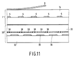
- FIG. 11 illustrates schematically and in only the brief outline necessary for comprehension a cross-section through such a combined display and image sensor.
- the substrate 2 of an image sensor 1 (for example any of the ones described above with reference to Figures 1 to 9) in accordance with the invention is mounted directly on top of the upper substrate 33 of the LCD display 30 so that the LCD display has to be viewed through the image sensor 1.
- the substrates 2 and 33 may, if desired, be secured together by means of a suitable transparent adhesive or the image sensor 1 may be removably mounted on top of the display device 30.
- Figure 11 shows a document D to be sensed being placed on top of the image sensor 1.
- the two device structures can be formed so that their row and column conductors are aligned and coincident.
- the opaque row conductors 5 of the image sensor 1 can be aligned with the light shield areas 38 of the LCD display.
- the display 30 may be secured to the image sensor 1 by means of, for example, a UV (ultra violet) curable epoxy resin and alignment may be achieved by, prior to UV exposure, flood illuminating the image sensor 1 with the back light of the display 30 and moving the image sensor 1 relative to the display 30 until a maximum light output (as detected by an appropriate meter) is achieved from the image sensor 1.
- the opaque row conductors 5 do not obstruct or obscure any of the image displayed by the LCD display and because the image sensor 1a is otherwise almost completely transparent any image displayed by the LCD display can be viewed in its entirety without any difficulty.
- the fact that the photosensitive elements 4a are provided on the opaque row conductors 5 means that the photosensitive elements are automatically shielded from the back illumination light source 0 of the liquid crystal display device.
- an image sensor such as those described above with reference to Figures 4 and 9 where a number of photosensitive elements are associated with the same pair of row and column conductors has particular advantages in that it enables the image sensor to have a resolution greater than the display device 30 to enable, for example, the reading or imaging of text, without having to have an increased number of row and column conductors which would otherwise reduce the transparency of the sensor and obscure part of the display.
- the image data signals read-out from the image sensor 1 may, possibly via an appropriate store such as a frame store, be supplied to the display device. This should enable the image sensor 1 to be used to 'write' on the display or to otherwise modify a displayed image using for example a light pen.
- a colour LCD display could be used together with a 'grey scale' image sensor to enable the image sensor to sense a full colour image by for example using the display to illuminate the sensor sequentially with red, green and blue light.
- the sets of image signals sensed by the image sensor 1 under each of these different colour illuminations can then be read out sequentially via the read-out amplifiers and combined to produce a composite set of signals representing the full colour image.
- This has the advantage that the image sensor itself need not be adapted for colour sensing.
- photosensitive elements such as amorphous silicon diodes, which are sensitive over the entire visible range should be used and that weighting factors may need to be incorporated when combining the signals to take account of the variation of quantum efficiency with wavelength.
- the image sensor may, as described above with reference to Figures 10 and 11 in conjunction with Figure 4 or 9,have a higher resolution than the display because the light passing through the display is not strictly parallel but diverges and because generally the separation of the liquid crystal display plane and the imaging plane, as set by the thickness of the substrates at typically about 2mm, is much greater than the pixel pitch which may be typically 200 ⁇ m (micrometres).
- the divergence of the light emitted by the LCD display under each separate colour illumination is such that the entire area of the document or object to be imaged is illuminated although only a third of the area of the display is generating the illumination.
- colours other than red, green and blue for example white plus two primary or two secondary (cyan, megneta or yellow) colours or the three secondary colours could be generated by the display and used to provide such a full colour sensor.
Abstract

Description
- This invention relates to an image sensor comprising a transparent substrate supporting a two dimensional array of photosensitive and switching elements and switching signal conductors and data signal conductors connected to the photosensitive and switching elements for enabling individual photosensitive elements to be accessed, the photosensitive and switching elements and conductors being arranged such that at least half of the area of the image sensor is transparent during operation.
- Such an image sensor is described in EP-A-378593 (International Publication No. WO 89/09960). The image sensor described in that document has a matrix array of photosensitive diodes connected back to back with switching diodes between row and column conductors. Each photosensitive diode may be formed on top of the associated switching diode. The image sensor is designed to be placed on top of, for example, an electro-optic display which requires the image sensor to be sufficiently transparent that the image produced by the display is still identifiable when viewed through the image sensor. As indicated in the document, the photosensitive diodes are designed to occupy equal to or less than 50% of the surface area of the image sensor. Clearly, the smaller the area occupied by the photosensitive diodes the better the view of the display image which can be obtained through the image sensor. However, the light collection efficiency of the photosensitive diodes reduces with area. It is accordingly necessary to accept a compromise between the dynamic range (that is the detection limit or number of gray scale levels which can be detected under a given illumination level) of the image sensor and the degree of obscuration of the display device.
- It is an aim of the present invention to provide an image sensor which is highly transparent but which also has a good dynamic range to enable efficient image detection.
- According to a first aspect of the present invention, there is provided an image sensor comprising a transparent substrate supporting a two dimensional array of photosensitive and switching elements with switching signal conductors and data signal conductors connected to the photosensitive and switching elements for enabling individual photosensitive elements to be accessed, the photosensitive and switching elements and conductors being arranged such that at least half of the area of the image sensor is transparent during operation, characterised in that each photosensitive element is electrically coupled to a respective capacitor for storing charge generated as a result of light being incident on the photosensitive element, the capacitors being formed so as to be transparent and so as to occupy a significant part of the entire area of the array.
- As used herein the term 'light' normal means electromagnetic radiation visible to the human eye but could be applied, by the use of appropriate materials to form the photosensitive elements, to electromagnetic radiation in, for example, the near infra-red and the term 'transparent' means that the material concerned absorbs very little, for example less than about 20%, of the light incident thereon.
- Thus, by storing charge generated as a result of light being incident on the photosensitive elements, the transparent capacitors act effectively to increase the dynamic range of the photosensitive elements by enabling a high quantity of charge to be stored in response to light incident on the photosensitive elements. The light capturing area of the photosensitive elements can therefore be quite small while still providing sufficient signal to enable high accuracy in the sensing of an image. The array may be, for example, up to about 90% transparent enabling it to be provided over, probably in contact with, a display device (which may be a cathode ray tube or other form of electro-optic display device such as a liquid crystal display device) without the image sensor unduly interfering with the image projected by the display device during its normal use. Where at least the switching signal conductors are opaque, the photosensitive elements may be shielded from the transparent substrate by the switching signal conductors. Thus, the photosensitive elements may be provided on top of the opaque switching signal conductors which reduces the area of the image sensor occupied by non-transparent components while shielding the photosensitive elements from light directed at the substrate for example from an electro-optic display on which the image sensor is mounted.
- Two or more photosensitive elements may be associated with the same pair of switching signal and data signal conductors and arranged to have different switching signal thresholds, for example by being associated with switching elements with different switching thresholds, so that the two or more photosensitive elements can be accessed separately by applying different threshold switching signals to the switching signal conductor.
- In another aspect, the present invention provides an image sensor comprising a transparent substrate supporting a two dimensional array of photosensitive and switching elements and switching signal conductors and data signal conductors connected to the photosensitive and switching elements for enabling individual photosensitive elements to be accessed, the photosensitive and switching elements and conductors being arranged such that a substantial part for example at least about half, of the area of the image sensor is transparent, the switching signal conductors being opaque and the photosensitive and switching elements being provided on the switching signal conductors so as to be shielded from the transparent substrate characterised in that two or more photosensitive elements are associated with the same pair of switching signal and data signal conductors and are arranged to have different switching signal thresholds so that the two or more photosensitive elements can be accessed separately by applying different threshold switching signals to the switching signal conductor.
- This enables the number of conductors to be reduced with respect to the number of photosensitive elements which should enable a greater area of the image sensor to be transparent whilst still achieving the same or similar resolution. Where the image sensor is to be provided on top of an active matrix-addressed electro-optic display this should enable the image sensor to have the same number of switching signal and data conductors as the display, so allowing the switching signal and data conductors of the image sensor to be aligned with the corresponding conductors of the display device and in particular with any mask used to shield the display switching elements from incident light. This should allow minimum, if any,obscuration of the display image by the image sensor while allowing the image sensor to have a higher resolution than the display. This should enable the image sensor to be able to sense or read text and should allow for optical character recognition with appropriate circuitry and software.
- Each switching element may comprise a diode or a number of series-connected diodes. In another example each switching element may comprise an insulated gate field effect transistor and the transistors associated with different ones of the two or more photosensitive elements may have different threshold voltages by, for example, providing a respective voltage-adjusting element between the gate electrode of the transistor and the switching signal conductor.
- The present invention also provides a method of forming a colour image sensor which method comprises providing an image sensor in accordance with the first aspect of the invention on a colour display device, for example a liquid crystal display device, activating the colour display device so as to illuminate an image being sensed by the image sensor sequentially with three different colours of light, reading out sets of signals from the image sensor representing the image as sensed under each different colour illumination and combining the three sets of signals to produce a set of composite signals representing the full colour image.
- With such an arrangement there is no need to provide colour filters within the image sensor and the image sensor can be adapted for colour image sensing simply by combining it with a conventional colour display. Although a Cathode Ray Tube (CRT) display device could be used, the use of a colour active matrix addressed display device has advantages because such a display is flat and compact allowing for formation of an easily portable device.
- Any suitable three 'colours' of light may be used for example the three primary (red, green and blue) or the three complementary (cyan, magenta and yellow) may be used. As a possible alternative one of the colours of light may be white light and the other two may be any selected two of the complementary colours).
- Embodiments of the invention will now be described, by way of example, with reference to the accompanying drawings, in which:
- Figure 1 is a schematic circuit layout of one example of an image sensor in accordance with the invention;
- Figure 2 is a schematic plan view of part of the image sensor shown in Figure 1 but illustrating only the conductive levels so as to show the geometric relationship between various components;
- Figure 3 is a cross-sectional view of part of the image sensor shown in Figure 1 taken along line III-III in Figure 2;
- Figure 4 is a schematic circuit layout of one image area of a modified version of the image sensor shown in Figure 1;
- Figure 5 is a cross-sectional view of part of a modified version of the image sensor shown in Figure 1 taken along the line V-V in Figure 2;
- Figure 6 is a schematic circuit layout of another example of an image sensor in accordance with the invention;
- Figure 7 is a schematic plan view of part of the image sensor shown in Figure 6 but illustrating only the conductive levels so as to show the geometric relationship between various components;
- Figure 8 is a cross-sectional view of part of the image sensor shown in Figure 6 taken along the line VIII-VIII in Figure 6;
- Figure 9 is a schematic circuit layout of one image area of a modified version of the image sensor shown in Figure 6;
- Figure 10 is a cross-sectional view of a picture element area of a liquid crystal display device; and
- Figure 11 is a cross-sectional view of a combined image sensor and display device in accordance with the invention.
- It should of course be understood that the drawings are merely schematic and are not to scale, for example various dimensions, such as the thickness of layers, may have been relatively exaggerated in the interests of clarity.
- Referring now to the drawings, there are illustrated various examples of image sensors in accordance with the invention. In each case, the
image sensor transparent substrate 2 supporting a twodimensional array 3 of photosensitive and switchingelements 4 withswitching signal conductors 5 anddata signal conductors 6 connected to the photosensitive and switchingelements 4 for enabling individual photosensitive elements to be accessed, the photosensitive and switchingelements 4 and theconductors - In accordance with the invention, each photosensitive element is electrically coupled to a
respective capacitor 7 for storing charge generated as a result of light being incident on the photosensitive element, thecapacitors 7 being formed so as to be transparent and so as to occupy a significant part of the entire area of thearray 3, where the term 'significant part' should be understood to mean at least 10% and preferably 50% or more of the area not occupied by the switching signal anddata signal conductors - By storing charge generated as a result of light being incident on the
photosensitive elements 4a, the transparent capacitors act effectively to increase the sensitivity of the photosensitive elements by enabling a high quantity of charge to be stored in response to light incident on the photosensitive elements. This means that the light capturing area of thephotosensitive elements 4 can be quite small while still providing sufficient signal to enable high accuracy in the sensing of an image. The array may be, for example, up to about 90% transparent enabling it to be provided over, probably in contact with, a display device which may be a cathode ray tube or other form of electrooptic display device such as a liquid crystal display device, without the image sensor unduly interfering with the image projected by the display device during its normal use. - Such an image sensor may be used, for example, to enable a contact image to be obtained merely by placing the document to be imaged onto the top of the combined display and image sensor. The image of the document may then be displayed by use of conventional electronic and video circuitry to transfer the stored image directly to the display device. As another example, the image sensor may be used to enable a light pen or similar device to be used to 'write' onto the display of a conventional cathode ray tube or liquid crystal display device.
- Figure 1 is a schematic circuit layout of one example of an image sensor 1a in accordance with the invention.
- In the example illustrated in Figure 1, the
array 3 may have an overall size of up to 400 by 400mm with a pitch between adjacent photosensitive and switching elements of about 200µm. For convenience only part of thearray 3 is shown in full. Each photosensitive element may be a diode, generally a p-i-n diode, which may also form the switching element. This diode is given thereference numeral 4 in Figure 1. In this case each photosensitive and switchingelement 4a is connected in series with thecapacitor 7 between a switching signal orrow conductor 5 and a data signal orcolumn conductor 6 so that each photosensitive and switchingelement 4a is associated with a unique pairing of row andcolumn conductors photosensitive element 4 to be accessed individually. - As illustrated in Figure 1 the row and
column conductors row conductors 5 are connected to a row driver or decoder/addressingcircuit 8 while thecolumn conductors 6 are connected including a charge-sensitive read-out amplifier arrangement 9 which may be of conventional type. A read-out arrangement of the type described in EP-A-440282 could also be used. - The matrix array of row and
column conductors image areas 10 each of which is bounded by two adjacent pairs of intersecting row andcolumn conductors image area 10 is associated with a single photosensitive and switchingelement 4a. - In the example of Figure 1, each photosensitive and switching
element 4a is reverse-biassed by appropriate switching signals on therow conductors 5 in order to enable sensing of an image so as to allow charge to be stored on theassociated capacitor 7. Each photosensitive and switchingelement 4a may then be forward-biassed in succession to enable the charge stored in the associatedcapacitor 7 to be read-out. Systems for addressing individual photosensitive elements and reading the charge (data) stored thereat are well known to the image sensing art (see for example EP-A-233104, EP-A-234968) and have derived, for example, from the active matrix addressing systems used for electro-optic, in particular LCD, displays. Accordingly, the details of the addressing and reading systems will not be given. - Figure 2 illustrates very schematically a plan view of the top conductive levels of an
image area 10 of the image sensor 1a together with at least parts of the row andcolumn conductors image area 10 shown in Figure 2. - In this example the
transparent substrate 2 is formed of glass, although other materials even flexible materials such as suitable plastics materials could be used. The image sensor 1a is formed upon thetransparent substrate 2 using conventional thin film processing techniques. Thus, in this case, therow conductors 5 are first formed by depositing and patterning a layer of a suitable opaque electrically conductive material, in this example chrome. The photosensitive and switchingelements 4a are then formed as, preferably, n-i-p (with the p conductivity layer adjacent the chromium row conductors 5) diodes, although p-i-n diodes could be used, by depositing and then patterning appropriately dopedlayers layer 11, for example of silicon oxide or silicon nitride is then deposited and patterned to form a window to enable contact to be made to thediodes 4a. - A layer of a transparent electrically conductive material, generally indium tin oxide, is then deposited and patterned to define the top contacts 12 to the
diodes 4. The top contact 12 of eachdiode 4 is formed integrally with the bottomtransparent electrode 7a of the associatedcapacitor 7. Alayer 13 of a transparent insulating material, such as silicon oxide or silicon nitride, is then deposited to form the capacitor dielectric followed by a layer of a transparent electrically conductive material, again generally indium tin oxide, which is patterned to define thetop electrodes 7b of thecapacitors 7 and thecolumn conductors 6. The conductivity of thecolumn conductors 6 may, if necessary, be increased by depositing and patterning, for example, an aluminium layer so as to provide a composite structure for thecolumn electrodes 6. The completed structure is generally be covered by a protective transparent insulatinglayer 14 such as a layer of polyimide. - As indicated schematically in Figures 2 and 3, the
transparent capacitors 7 occupy a significant part of theimage areas 10. Depending upon the particular application, the capacitors may have a capacitance in the range of from about 0.1 to about 5pF (picofarads). The actual proportion of eachimage area 10 occupied by thecapacitor 7 will generally be most dependent on the pixel pitch (that is the distance between the centres of adjacent image areas 10) because it is likely that similar capacitances will be required even if the pixel pitches are different. Thus, for example, where the pixel pitch is about 0.1mm (millimetres) then thecapacitor 7 might occupy between 50% and 100% of thearea 10 not occupied by theconductors area 10 occupied by thecapacitors 7 may fall to 10% to 20% for a similar capacitance although, of course, larger capacitances could be used. It will be appreciated that, although the use of extremely large area, (for example occupying 80% to 100% of theimage area 10 as shown in Figures 2 and 3) may be advantageous in further increasing the dynamic range, even materials such as indium tin oxide (ITO) absorb a small amount of light and thus reduce the transparency of the device. In addition, the larger the area of the capacitors the more likely is the possibility of short-circuits due to pin-hole defects. - The photosensitive and switching
elements 4a are provided on top of theopaque row conductors 5 which has the advantages of automatically shielding the photosensitive and switchingelements 4a from light transmitted through thesubstrate 2 towards the photosensitive and switchingelements 4a and in addition means that the photosensitive element (which of course must absorb the light to be sensed and cannot therefore be transparent) is provided on an area of the image sensor 1a which is already opaque. Accordingly, the amount of the image sensor 1a area which is opaque need not in any way affected by the presence of the photosensitive and switchingelements 4a. Typically, as much as 90% of the entire area of the image sensor 1a may be transparent. - Figure 4 is a circuit layout of one
image area 10 for illustrating a modification of the circuit shown in Figure 1 which enables an even greater proportion of the area of the image sensor to be transparent. - In the
image sensor 1b illustrated by way of thesingle image area 10 in Figure 4, a number of photosensitive and switchingelements 4 are associated with the same pair of row andcolumn conductors elements 4a to be accessed,threshold adjusting devices 14 are provided so that a different level of switching signal is required on therow conductor 5 to access different ones of the photosensitive elements associated with the same pair of row andcolumn conductors threshold adjusting devices 14 are in the form of additional diodes connected in series with the diodes forming the photosensitive and switchingelements 4a. As shown in Figure 4, three photosensitive and switchingelement diodes 4a are associated with the same pair of row andcolumn conductors elements image area 10. - The number of series-connected
additional diodes 14 used to adjust the threshold voltage at which a givenphotosensitive diode 4a can be accessed will of course depend on the characteristics of thethreshold adjusting diodes 14 and the switching signal voltage levels which are available. - The
threshold adjusting diodes 14 may be formed on theopaque row conductors 5 in a similar manner to thephotosensitive diodes 4a. Thethreshold adjusting diodes 14 need of course to be shielded from the light to be detected by thephotosensitive diodes 4a. This may be achieved by forming the respectivephotosensitive diode 4 on top of the associated threshold adjusting diode ordiode stack 14 or by providing an opaque (generally chromium) top contact for thethreshold adjusting diodes 14. - The separate capacitors 7', 7'' and 7''' in the example shown in Figure 4 may be formed quite simply by patterning of the indium tin oxide layers in appropriate manner to define, in this case, three discrete capacitors of any desired geometry in each
image area 10. The separate capacitors 7', 7'' and 7''' may all be of the same or similar size so that each provides a similar value signal, thereby simplifying processing. Alternatively, the separate capacitors 7', 7'' and 7''' may have significantly different areas (and thus capacitances) which may facilitate identification of the particular capacitor supplying a signal, at the expense of further processing circuitry. In particular the capacitor 7' may be smaller than the capacitor 7'' which may in turn be smaller than the capacitor 7'''. This may assist in ensuring that, when its signal is readout, each capacitor is fully discharged before the signal is read from the next higher threshold subsidiary pixel. - An
image sensor 1b havingimage areas 10 with the structure shown in Figure 4 has the additional advantage that, as a unique pair of row andcolumn conductors column conductors image sensor 1b taken up by theopaque conductors image sensor 1b to be transparent. - In the examples described above, the photosensitive and switching elements are provided by a single
photosensitive diode 4a. However, the photosensitive elements may be separated from the switching elements. In such a case, the photosensitive elements do not need to have a switching capability and could be for example photosensitive resistors. - Figures 1 and 4 illustrate in phantom lines the use of a separate
photosensitive element 4b. As shown, the photosensitive element is aphotosensitive diode 4b arranged in parallel with the associatedcapacitor 7. Thisphotosensitive diode 4b is indicated by dashed lines in Figure 4. Figure 5 illustrates a possible structure for such aphotosensitive diode 4b. As can be seen from Figure 5, thephotosensitive diode 4b has a similar structure to that shown in Figure 3 for the combined photosensitive and switchingdiode 4a except that, of course, thephotosensitive diode 4b is electrically isolated from theopaque row conductor 5 by an insulatinglayer 15 and the indium tin oxide layers providing the bottom andtop electrodes capacitor 7 are patterned so as to define the bottom and top electrodes 4'b and 4''b, respectively, of thephotosensitive diode 4b. - In this case, the other diode labelled 4a in Figures 1 and 4 is not intended to be photosensitive and should be shielded from the light incident on the image sensor in a manner similar to that described above in relation to the
threshold adjusting diodes 14. - Although the switching element and
threshold adjusting diodes photosensitive elements 4b (shown in dashed lines in Figures 1 and 4) or as the combined photosensitive and switchingelements 4a described above. - In each of the above modifications, the photosensitive and switching elements may be formed on the
opaque row conductors 5 so as to leave a maximum amount of eachimage area 10 free to be occupied by the transparent capacitor orcapacitors 7. - It will be appreciated that other circuit arrangements and combinations of two-terminal photosensitive and switching elements may be used to form an image sensor in accordance with the invention.
- Figure 6 illustrates another example of an
image sensor 1c in which three-terminal switching elements, as shown thin film insulated gate field effect transistors (TFTs), 4c may be used in place of the two-terminal switching elements described above. In this case, the control or gate electrode of eachTFT 4c is connected to arow conductor 5 while one of the main electrodes (in this case the source electrode) is connected to acolumn conductor 6. The other (drain) electrode of eachTFT 4c is connected to the parallel arrangement of thephotosensitive element 4b andcapacitor 7. Again thephotosensitive element 4b may, as shown, be a diode although other photosensitive elements such as a photosensitive resistor or diode-connected photosensitive TFT may be used. The anode of thephotosensitive diode 4b is connected to acommon line 16 which is connected to a reference potential. - In operation of the
image sensor 1c, light incident on thephotosensitive elements 4a is stored as charge on thecapacitors 7. this charge is read-out via thecolumn conductors 6 when the associatedTFT 4c is rendered conducting by application of an appropriate switching signal to theappropriate row conductor 5. - Figure 7 is a schematic plan view of the electrode layout of the
image sensor 1c. The region of theTFT 4c is indicated generally by an arrowed line as is the region of thephotosensitive diode 4b Figure 8 is a cross-sectional view of such animage area 10 to show the structure of aTFT 4c. - As can be seen from Figures 7 and 8, in this case the
TFT 4c may be formed on top of therow conductor 5 which forms the gate line connecting all the gates of a row ofTFTs 4c. TheTFT 4c shown in Figure 8 is an inverted type B TFT having a generallychromium gate electrode 17a which may be provided directly on top of therow conductor 5. - Various layers are deposited and patterned to build up the
TFTs 4c. EachTFT 4c has agate insulating region 17b, generally formed of silicon dioxide or silicon nitride, covered by a channel-formingintrinsic semiconductor region 18, for example an amorphous or polycrystalline silicon region.Doped semiconductor regions 19 may be provided to define source and drain contact regions between the channel-formingregion 18 and source and drainelectrodes layer 22 may be provided over the channel region. - A transparent insulating
layer 23 generally of silicon dioxide or silicon nitride is provided over the surface of the structure and patterned to define windows to enable contact to be made to the source and drainelectrodes opaque column conductors 6 connecting the source electrodes of eachTFT 4c in a column of TFTs and transparent, generally indium tin oxide (ITO), drain conductors which extend to form thebottom electrodes 7a of thecapacitors 7. - A further transparent insulating
layer 13 is provided over the structure followed by a further transparent, generally ITO, layer which provides, as an integral metallisation, thetop electrodes 7b of thecapacitors 7 and thecommon line 16. This is followed by a protectivetransparent passivating layer 14 which is generally a polyimide layer. - The
photosensitive diodes 4b may be formed with theTFTs 4c or separately using appropriate masks to enable the respective device characteristics to be optimised. Thephotosensitive diodes 4b may have a structure similar to that shown in Figure 5 where, of course, in this example thetop electrode 7b of the capacitor also forms thecommon electrode 16. - Again, as in the examples described with reference to Figure 1, the proportion of each
image area 10 which can be occupied by thetransparent capacitor 7, or may be free of components and thus transparent, can be increased by as described above providing the photosensitive and switchingelements row conductors 5. - Figure 9 illustrates an
image area 10 of a modified version 1d of theimage sensor 1c. The image sensor 1d is related to theimage sensor 1c in a similar manner as theimage sensor 10 of Figure 1 is related to theimage sensor 1b of Figure 4. Thus, in the image sensor 1d, each unique pair of row andcolumn conductors image area 10 is associated with a number ofphotosensitive elements 4b each with itsown switching element 4c. In this case the threshold adjusting means necessary to enable access, as described above in relation to Figure 4, of individualphotosensitive elements 4b adjusts the gate voltage necessary to turn on aparticular TFT 4c. This may be achieved by using TFTs with different gate threshold voltages, by for example adjusting the gate insulating region thickness, or by the insertion between the gate electrode 17 and therow conductor 5 of a threshold adjusting device for example a capacitor 24 (shown in phantom lines in Figure 9) or a diode or similar device. In other respects the image sensor 1d is similar to theimage sensor 1c. The image sensor 1d enables access of individualphotosensitive elements 4b in a manner similar to that described above with reference to Figure 4. - It will of course be appreciated that various different circuit configurations, be they diode switching or TFT switching arrangements, may be used. Moreover, the photosensitive and switching elements need not necessarily be provided on top of the
row conductors 5 although this would necessarily reduce somewhat the proportion of eachimage area 10 which could be made transparent. - When each
image area 10 is associated with a number ofphotosensitive elements 4 then these may be made sensitive to different wavelengths, for example by the incorporation of colour filters in a manner similar to that known for electro-optic displays such as liquid crystal displays, so as to enable colour image sensing. - The image sensors described above may be used, for example, to form an image of a document placed directly upon the transparent
protective layer 14. - In each of the examples described above, charge stored on the
capacitors 7 representing an image sensed by thephotosensitive elements 4b is read out via the read-outamplifier 9 by accessing eachphotosensitive element 4b and the associatedcapacitor 7 individually as described above. The image signal data thus obtained may be supplied, for example, to a frame store for subsequent display on a display device such as a cathode ray tube or other electrooptic display device for example a liquid crystal display device. Alternatively the image signal data may be stored on an appropriate medium, WORM, RAM etc. for later use or may be subject to computer processing before storage or display. - As described above, an image sensor in accordance with the invention can be made very transparent, potentially in the region of 70 to 80% transparent. This enables the image sensor to be placed over or mounted on top of a display device whilst still enabling the display to be viewed. Such a display may be, for example, a cathode ray tube (CRT), a liquid crystal (LCD) or other electro-optic display or any other form of visual display (such as an instrumentation display panels using the image sensor as a convenient way of inputting data). If the
transparent substrate 2 of the image sensor can be made of a flexible, for example plastics, material and enable the entire image sensor to have some degree of flexibility it may be possible to apply image sensor in accordance with the invention to a conventional CRT or other display having a curved surface. Also, with appropriate electronic circuitry of conventional type it may be possible to allow the data to be input to the display via, for example, a light pen or directly from a document placed on the image sensor. - An image sensor in accordance with the present invention may have particular applications in relation to LCD or similar active matrix addressed displays. The usual form of a liquid crystal display device is well known and will not be described in detail here. Generally speaking the circuit layout of an active matrix addressed LCD display will be similar to that of the image sensor shown in Figure 1 or Figure 6 with of course several important differences. In particular, the photosensitive elements will generally be omitted and the capacitors, while present, will be those provided by the liquid crystal material and associated electrodes. The switching elements represented as diodes in Figure 1 may in the case of an LCD display be any suitable form of non-linear switching device such as p-i-n diodes, MIMs etc.
- In the case of a liquid crystal display the respective areas, corresponding to the
image areas 10, bounded by the row and column conductors, are normally known as picture elements or pixels. - Figure 10 is a cross-sectional view through one
pixel 31 of a liquidcrystal display device 30 having a TFT switching element based active matrix array. Generally, the circuit layout in this case will be similar to that shown for the image sensor in Figure 6 except that, again, the photosensitive elements will generally be omitted and the capacitors represent the capacitances of the liquid crystal display elements. - For more detailed information on LCD displays reference made be made to, for example, US Patent No. 3862360 or a paper entitled 'Liquid Crystal Matrix Displays' by Lechner et al published in the Proceedings of the IEEE Vol. 59, No. 11, November 1971 at pages 1566-1579 or any readily available standard text.
- The
liquid crystal display 30 has two spaced-apart transparent, normally glass,substrates liquid crystal material 34 is disposed. Although not shown, polarising layers are normally provided on the outer surfaces of thesubstrates - The
upper substrate 33 carries a transparent, generally ITO, electrode which forms thecommon electrode 34 of thepicture elements 31. Thelower substrate 32 carries theswitching elements 35 which in this example are of similar structure to that described above with reference to Figure 8 and will not be described further. The same reference numerals have been used in Figure 10 as in Figure 8. In this case, however, the ITO drain electrode of eachTFT 35 extends to form alower electrode 36 of the picture element and the passivating insulatinglayer 13 is covered by anorientation layer 37 of a polymer material. - The transparent
common electrode 34 carries a light shield in the form of a matrix oflight shielding areas 38 of insulative material which act to shield the switchingelements 35 from scattered light or light incident on theupper substrate 32. Thecommon electrode 34 may also carry acolour filter layer 39 which defines a matrix of adjacent filter regions of red, green and blue filter material arranged in known manner so that the outputs from the corresponding group of three picture elements can combine to produce a colour image. Afurther orientation layer 40 is provided between the liquid crystal material and thelight shielding areas 38. - As described in, for example, GB-A-2198969 or EP-A-271960, each
picture element 31 may be divided into subsidiary picture elements accessible by respective switching elements with some appropriate form of threshold adjusting device being provided to enable different subsidiary picture elements associated with the same pair of row and column conductors to be accessed individually by the use of different switching signals so as to improve the grey scale (or colour resolution) of the image which can be produced by the display. - An image sensor in accordance with the invention may be combined with an LCD display of the type described above. Figure 11 illustrates schematically and in only the brief outline necessary for comprehension a cross-section through such a combined display and image sensor.
- As shown in Figure 11, the
substrate 2 of an image sensor 1 (for example any of the ones described above with reference to Figures 1 to 9) in accordance with the invention is mounted directly on top of theupper substrate 33 of theLCD display 30 so that the LCD display has to be viewed through theimage sensor 1. Thesubstrates image sensor 1 may be removably mounted on top of thedisplay device 30. Figure 11 shows a document D to be sensed being placed on top of theimage sensor 1. - Because the
LCD display 30 andimage sensor 1 have similar active matrix addressing arrangements, the two device structures can be formed so that their row and column conductors are aligned and coincident. In particular, theopaque row conductors 5 of theimage sensor 1 can be aligned with thelight shield areas 38 of the LCD display. Thedisplay 30 may be secured to theimage sensor 1 by means of, for example, a UV (ultra violet) curable epoxy resin and alignment may be achieved by, prior to UV exposure, flood illuminating theimage sensor 1 with the back light of thedisplay 30 and moving theimage sensor 1 relative to thedisplay 30 until a maximum light output (as detected by an appropriate meter) is achieved from theimage sensor 1. This means that theopaque row conductors 5 do not obstruct or obscure any of the image displayed by the LCD display and because the image sensor 1a is otherwise almost completely transparent any image displayed by the LCD display can be viewed in its entirety without any difficulty. The fact that thephotosensitive elements 4a are provided on theopaque row conductors 5 means that the photosensitive elements are automatically shielded from the back illumination light source 0 of the liquid crystal display device. - The use of an image sensor such as those described above with reference to Figures 4 and 9 where a number of photosensitive elements are associated with the same pair of row and column conductors has particular advantages in that it enables the image sensor to have a resolution greater than the
display device 30 to enable, for example, the reading or imaging of text, without having to have an increased number of row and column conductors which would otherwise reduce the transparency of the sensor and obscure part of the display. - With appropriate conventionally available circuitry the image data signals read-out from the
image sensor 1 may, possibly via an appropriate store such as a frame store, be supplied to the display device. This should enable theimage sensor 1 to be used to 'write' on the display or to otherwise modify a displayed image using for example a light pen. - As indicated above it may be possible to make the image sensor sensitive to colour so enabling writing in full colour on a colour LCD display.
- Alternatively, a colour LCD display could be used together with a 'grey scale' image sensor to enable the image sensor to sense a full colour image by for example using the display to illuminate the sensor sequentially with red, green and blue light. The sets of image signals sensed by the
image sensor 1 under each of these different colour illuminations can then be read out sequentially via the read-out amplifiers and combined to produce a composite set of signals representing the full colour image. This has the advantage that the image sensor itself need not be adapted for colour sensing. It will of course be appreciated that photosensitive elements, such as amorphous silicon diodes, which are sensitive over the entire visible range should be used and that weighting factors may need to be incorporated when combining the signals to take account of the variation of quantum efficiency with wavelength. The image sensor may, as described above with reference to Figures 10 and 11 in conjunction with Figure 4 or 9,have a higher resolution than the display because the light passing through the display is not strictly parallel but diverges and because generally the separation of the liquid crystal display plane and the imaging plane, as set by the thickness of the substrates at typically about 2mm, is much greater than the pixel pitch which may be typically 200µm (micrometres). This means that the divergence of the light emitted by the LCD display under each separate colour illumination is such that the entire area of the document or object to be imaged is illuminated although only a third of the area of the display is generating the illumination. - Of course colours other than red, green and blue (for example white plus two primary or two secondary (cyan, megneta or yellow) colours or the three secondary colours could be generated by the display and used to provide such a full colour sensor.
- From reading the present disclosure, other modifications and variations will be apparent to persons skilled in the art. Such modifications and variations may involve other features which are already known in the semiconductor art and which may be used instead of or in addition to features already described herein. Although claims have been formulated in this application to particular combinations of features, it should be understood that the scope of the disclosure of the present application also includes any novel feature or any novel combination of features disclosed herein either explicitly or implicitly, whether or not it relates to the same invention as presently claimed in any claim and whether or not it mitigates any or all of the same technical problems as does the present invention. The applicants hereby give notice that new claims may be formulated to such features and/or combinations of such features during the prosecution of the present application or of any further application derived therefrom.
Claims (14)
- An image sensor comprising a transparent substrate supporting a two dimensional array of photosensitive and switching elements with switching signal conductors and data signal conductors connected to the photosensitive and switching elements for enabling individual photosensitive elements to be accessed, the photosensitive and switching elements and conductors being arranged such that at least half of the area of the image sensor is transparent during operation, characterised in that each photosensitive element is electrically coupled to a respective capacitor for storing charge generated as a result of light being incident on the photosensitive element, the capacitors being formed so as to be transparent and so as to occupy a significant part of the entire area of the array.
- An image sensor according to Claim 1, wherein at least the switching signal conductors are opaque and the photosensitive elements are provided on the switching signal conductors so as to be shielded from the transparent substrate by the switching signal conductors.
- An image sensor according to Claim 1 or 2, wherein two or more photosensitive elements are associated with the same pair of switching signal and data signal conductors and are arranged to have different switching signal thresholds so that the two or more photosensitive elements can be accessed separately by applying different threshold switching signals to the switching signal conductor.
- An image sensor comprising a transparent substrate supporting a two dimensional array of photosensitive and switching elements and switching signal conductors and data signal conductors connected to the photosensitive and switching elements for enabling individual photosensitive elements to be accessed, the photosensitive and switching elements and conductors being arranged such that a substantial part of the area of the image sensor is transparent, the switching signal conductors being opaque and the photosensitive and switching elements being provided on the switching signal conductors so as to be shielded from the transparent substrate characterised in that two or more photosensitive elements are associated with the same pair of switching signal and data signal conductors and are arranged to have different switching signal thresholds so that the two or more photosensitive elements can be accessed separately by applying different threshold switching signals to the switching signal conductor.
- An image sensor according to Claim 3 or 4, wherein the different switching signal thresholds are provided by connecting each of the two or more photosensitive elements to the associated switching signal conductor by separate switching elements having different switching thresholds.
- An image sensor according to Claim 5, wherein each switching element comprises a diode or a number of series-connected diodes.
- An image sensor according to Claim 5, wherein each switching element comprises an insulated gate field effect transistor and the transistors associated with difference ones of the two or more photosensitive elements have different threshold voltages.
- An image sensor according to Claim 5, wherein each switching element comprises an insulated gate field effect transistor and a respective voltage-adjusting element is provided between the gate electrode of the transistor and the switching signal conductor.
- The combination of an electro-optic display device with an image sensor in accordance with any one of the preceding claims, wherein the image sensor is mounted to the display surface of the display device so that an image provided by the display device is viewed through the image sensor.
- The combination according to Claim 9, wherein the electro-optic display device comprises an active matrix display device having a transparent substrate supporting a two-dimensional array of picture elements and signal conductors and data signal conductors for enabling individual picture elements to be accessed via associated switching elements and wherein the display device conductors are aligned with the corresponding conductors of the image sensor.
- The combination according to Claim 10, wherein the display device carries a mask for shielding the switching elements from incident light and the switching signal conductors of the image sensor are aligned with the mask.
- The combination according to Claim 9,10 or 11, wherein the electro-optic display device is a colour display device.
- A method of forming a colour image sensor which method comprises providing an image sensor in accordance with any one of Claims 1 to 8 on a colour display device, activating the colour display device so as to illuminate an image being sensed by the image sensor sequentially with three different colours of light, reading out sets of signals from the image sensor representing the image as sensed under each different colour illumination and combining the three sets of signals to produce a set of composite signals representing the full colour image.
- A method according to Claim 13, which further comprises illuminating the image with red, green and blue light in any desired sequence.
Priority Applications (1)
| Application Number | Priority Date | Filing Date | Title |
|---|---|---|---|
| EP96200193A EP0710987A1 (en) | 1992-05-06 | 1993-05-03 | An image sensor |
Applications Claiming Priority (2)
| Application Number | Priority Date | Filing Date | Title |
|---|---|---|---|
| GB929209734A GB9209734D0 (en) | 1992-05-06 | 1992-05-06 | An image sensor |
| GB9209734 | 1992-05-06 |
Related Child Applications (2)
| Application Number | Title | Priority Date | Filing Date |
|---|---|---|---|
| EP96200193.9 Division-Into | 1993-05-03 | ||
| EP96200193A Division EP0710987A1 (en) | 1992-05-06 | 1993-05-03 | An image sensor |
Publications (2)
| Publication Number | Publication Date |
|---|---|
| EP0569090A1 true EP0569090A1 (en) | 1993-11-10 |
| EP0569090B1 EP0569090B1 (en) | 1998-01-14 |
Family
ID=10715058
Family Applications (2)
| Application Number | Title | Priority Date | Filing Date |
|---|---|---|---|
| EP93201253A Expired - Lifetime EP0569090B1 (en) | 1992-05-06 | 1993-05-03 | Image sensor |
| EP96200193A Ceased EP0710987A1 (en) | 1992-05-06 | 1993-05-03 | An image sensor |
Family Applications After (1)
| Application Number | Title | Priority Date | Filing Date |
|---|---|---|---|
| EP96200193A Ceased EP0710987A1 (en) | 1992-05-06 | 1993-05-03 | An image sensor |
Country Status (5)
| Country | Link |
|---|---|
| US (1) | US5349174A (en) |
| EP (2) | EP0569090B1 (en) |
| JP (1) | JP3955887B2 (en) |
| DE (1) | DE69316261T2 (en) |
| GB (1) | GB9209734D0 (en) |
Cited By (4)
| Publication number | Priority date | Publication date | Assignee | Title |
|---|---|---|---|---|
| EP1122792A2 (en) * | 2000-01-31 | 2001-08-08 | Semiconductor Energy Laboratory Co., Ltd. | Contact type area sensor and display device having contact type area sensor |
| US6703994B2 (en) | 2000-06-10 | 2004-03-09 | Koninklijke Philips Electronics N.V. | Active matrix array devices |
| US7123232B1 (en) | 1999-07-29 | 2006-10-17 | Koninklijke Philips Electronics N.V. | Active matrix array devices |
| EP2485261A3 (en) * | 2011-02-07 | 2013-12-11 | Samsung Electronics Co., Ltd. | Radiation detector and method for manufacturing the same |
Families Citing this family (61)
| Publication number | Priority date | Publication date | Assignee | Title |
|---|---|---|---|---|
| US5742709A (en) * | 1993-05-14 | 1998-04-21 | Fuji Xerox Co., Ltd. | Display panel for use with an image reading device |
| US6100951A (en) * | 1996-09-30 | 2000-08-08 | U.S. Philips Corporation | Thin-film switching elements for electronic devices and a method of manufacturing the same |
| US6011531A (en) * | 1996-10-21 | 2000-01-04 | Xerox Corporation | Methods and applications of combining pixels to the gate and data lines for 2-D imaging and display arrays |
| GB9710301D0 (en) * | 1997-05-21 | 1997-07-16 | Philips Electronics Nv | Image sensor and its manufacture |
| US5994713A (en) * | 1997-06-25 | 1999-11-30 | Quantum Imaging Corp. | Filmless photon imaging apparatus |
| JP4027465B2 (en) * | 1997-07-01 | 2007-12-26 | 株式会社半導体エネルギー研究所 | Active matrix display device and manufacturing method thereof |
| US6627305B1 (en) | 1997-07-16 | 2003-09-30 | Koninklijke Philips Electronics N.V. | Substrates for large area electronic devices |
| JP3838393B2 (en) * | 1997-09-02 | 2006-10-25 | 株式会社半導体エネルギー研究所 | Display device with built-in image sensor |
| JP4271268B2 (en) | 1997-09-20 | 2009-06-03 | 株式会社半導体エネルギー研究所 | Image sensor and image sensor integrated active matrix display device |
| US6207842B1 (en) * | 1997-10-09 | 2001-03-27 | Mars Incorporated | Process for preparing procyanidin(4-6 or 4-8) oligomers and their derivatives |
| JP4044187B2 (en) * | 1997-10-20 | 2008-02-06 | 株式会社半導体エネルギー研究所 | Active matrix display device and manufacturing method thereof |
| GB9725571D0 (en) * | 1997-12-04 | 1998-02-04 | Philips Electronics Nv | Electronic apparatus comprising fingerprint sensing devices |
| JPH11326954A (en) | 1998-05-15 | 1999-11-26 | Semiconductor Energy Lab Co Ltd | Semiconductor device |
| US6188056B1 (en) * | 1998-06-24 | 2001-02-13 | Stmicroelectronics, Inc. | Solid state optical imaging pixel with resistive load |
| US6690076B1 (en) | 1999-03-10 | 2004-02-10 | Micron Technology, Inc. | Stitched circuits larger than the maximum reticle size in sub-micron process |
| US6989916B2 (en) * | 2000-12-18 | 2006-01-24 | Hewlett-Packard Development Company, L.P. | Scanner screen using computer monitor as external light source |
| US7230597B2 (en) * | 2001-07-13 | 2007-06-12 | Tpo Hong Kong Holding Limited | Active matrix array devices |
| KR100432490B1 (en) | 2001-09-17 | 2004-05-22 | (주)니트 젠 | Optical fingerprint acquisition apparatus |
| US7023503B2 (en) * | 2002-02-20 | 2006-04-04 | Planar Systems, Inc. | Image sensor with photosensitive thin film transistors |
| US7009663B2 (en) | 2003-12-17 | 2006-03-07 | Planar Systems, Inc. | Integrated optical light sensitive active matrix liquid crystal display |
| WO2003073159A1 (en) | 2002-02-20 | 2003-09-04 | Planar Systems, Inc. | Light sensitive display |
| US7053967B2 (en) | 2002-05-23 | 2006-05-30 | Planar Systems, Inc. | Light sensitive display |
| US6740884B2 (en) * | 2002-04-03 | 2004-05-25 | General Electric Company | Imaging array and methods for fabricating same |
| US6777685B2 (en) * | 2002-04-03 | 2004-08-17 | General Electric Company | Imaging array and methods for fabricating same |
| US20060034492A1 (en) * | 2002-10-30 | 2006-02-16 | Roy Siegel | Hand recognition system |
| US20080084374A1 (en) | 2003-02-20 | 2008-04-10 | Planar Systems, Inc. | Light sensitive display |
| US20040246355A1 (en) * | 2003-06-06 | 2004-12-09 | Ji Ung Lee | Storage capacitor array for a solid state radiation imager |
| US6933191B2 (en) * | 2003-09-18 | 2005-08-23 | International Business Machines Corporation | Two-mask process for metal-insulator-metal capacitors and single mask process for thin film resistors |
| US20050134749A1 (en) * | 2003-12-19 | 2005-06-23 | Adiel Abileah | Reflection resistant display |
| US7773139B2 (en) | 2004-04-16 | 2010-08-10 | Apple Inc. | Image sensor with photosensitive thin film transistors |
| TWI250783B (en) * | 2004-12-17 | 2006-03-01 | Primax Electronics Ltd | Image scanning device |
| US7873356B2 (en) * | 2005-09-16 | 2011-01-18 | Microsoft Corporation | Search interface for mobile devices |
| US7933632B2 (en) | 2005-09-16 | 2011-04-26 | Microsoft Corporation | Tile space user interface for mobile devices |
| US20070067726A1 (en) * | 2005-09-16 | 2007-03-22 | Microsoft Corporation | Content sharing user interface for mobile devices |
| JP2009010075A (en) * | 2007-06-27 | 2009-01-15 | Fujifilm Corp | Radiation image detector |
| US7697131B2 (en) * | 2008-04-16 | 2010-04-13 | Fluke Corporation | Automated display quality measurement device |
| CN101609855B (en) * | 2008-06-20 | 2013-09-18 | 群康科技(深圳)有限公司 | Photosensitive capacitor, photosensitive circuit, substrate, manufacturing process thereof and display device |
| TWI547845B (en) * | 2009-07-02 | 2016-09-01 | 半導體能源研究所股份有限公司 | Touch panel and driving method thereof |
| US20110235156A1 (en) * | 2010-03-26 | 2011-09-29 | Qualcomm Mems Technologies, Inc. | Methods and devices for pressure detection |
| DE102010030108B4 (en) | 2010-06-15 | 2014-12-04 | Fraunhofer-Gesellschaft zur Förderung der angewandten Forschung e.V. | Color sensor |
| US9310923B2 (en) | 2010-12-03 | 2016-04-12 | Apple Inc. | Input device for touch sensitive devices |
| US8928635B2 (en) | 2011-06-22 | 2015-01-06 | Apple Inc. | Active stylus |
| US9329703B2 (en) | 2011-06-22 | 2016-05-03 | Apple Inc. | Intelligent stylus |
| US8638320B2 (en) | 2011-06-22 | 2014-01-28 | Apple Inc. | Stylus orientation detection |
| US9437132B2 (en) * | 2011-11-30 | 2016-09-06 | Apple Inc. | Devices and methods for providing access to internal component |
| US9176604B2 (en) | 2012-07-27 | 2015-11-03 | Apple Inc. | Stylus device |
| US9652090B2 (en) | 2012-07-27 | 2017-05-16 | Apple Inc. | Device for digital communication through capacitive coupling |
| US9557845B2 (en) | 2012-07-27 | 2017-01-31 | Apple Inc. | Input device for and method of communication with capacitive devices through frequency variation |
| JP6265655B2 (en) * | 2012-10-09 | 2018-01-24 | キヤノン株式会社 | Detection device and detection system |
| US10048775B2 (en) | 2013-03-14 | 2018-08-14 | Apple Inc. | Stylus detection and demodulation |
| JP6383516B2 (en) | 2013-04-19 | 2018-08-29 | ライトスピン テクノロジーズ、インク. | Integrated avalanche photodiode array |
| US10845901B2 (en) | 2013-07-31 | 2020-11-24 | Apple Inc. | Touch controller architecture |
| US9431453B2 (en) * | 2013-10-23 | 2016-08-30 | Avago Technologies General Ip (Singapore) Pte. Ltd. | Fill factor opto-sensitive device |
| US9582127B2 (en) | 2014-04-04 | 2017-02-28 | Synaptics Incorporated | Large feature biometrics using capacitive touchscreens |
| US10061450B2 (en) | 2014-12-04 | 2018-08-28 | Apple Inc. | Coarse scan and targeted active mode scan for touch |
| WO2016178678A1 (en) * | 2015-05-06 | 2016-11-10 | Lightspin Technologies, Inc. | Integrated avalanche photodiode arrays |
| US10437329B2 (en) | 2015-08-03 | 2019-10-08 | Fundació Institut De Ciències Fotòniques | Gaze tracking apparatus |
| ES2682097T3 (en) | 2015-08-03 | 2018-09-18 | Fundació Institut De Ciències Fotòniques | Image sensor with non-local reading circuit and optoelectronic device comprising said image sensor |
| KR20180112837A (en) * | 2016-02-12 | 2018-10-12 | 사빅 글로벌 테크놀러지스 비.브이. | Photosensitive laminate, manufacturing method and image sensor device |
| US10474277B2 (en) | 2016-05-31 | 2019-11-12 | Apple Inc. | Position-based stylus communication |
| US10529884B2 (en) | 2017-11-09 | 2020-01-07 | LightSpin Technologies Inc. | Virtual negative bevel and methods of isolating adjacent devices |
Citations (6)
| Publication number | Priority date | Publication date | Assignee | Title |
|---|---|---|---|---|
| GB2156133A (en) * | 1984-03-15 | 1985-10-02 | Int Standard Electric Corp | Reproducing graphical presentations on a display screen |
| EP0260824A2 (en) * | 1986-09-16 | 1988-03-23 | OIS Optical Imaging Systems, Inc. | Circuit for a photosensitive pixel with exposed blocking element |
| EP0271960A2 (en) * | 1986-12-19 | 1988-06-22 | Philips Electronics Uk Limited | Matrix display devices |
| EP0287228A2 (en) * | 1987-04-17 | 1988-10-19 | OIS Optical Imaging Systems, Inc. | Photoresponsive array |
| EP0319403A1 (en) * | 1987-12-04 | 1989-06-07 | Thomson-Csf | Matrix of photosensitive elements each comprising a diode or a diode and a memory capacitor |
| WO1989009960A1 (en) * | 1988-04-11 | 1989-10-19 | Thomson-Csf | Display and writing device |
Family Cites Families (7)
| Publication number | Priority date | Publication date | Assignee | Title |
|---|---|---|---|---|
| US3862360A (en) * | 1973-04-18 | 1975-01-21 | Hughes Aircraft Co | Liquid crystal display system with integrated signal storage circuitry |
| US4448491A (en) * | 1979-08-08 | 1984-05-15 | Canon Kabushiki Kaisha | Image display apparatus |
| US4388532A (en) * | 1981-04-27 | 1983-06-14 | Eastman Kodak Company | Solid state image sensor with image sensing elements having charge coupled photocapacitors and a floating gate amplifier |
| JPH0645753B2 (en) * | 1985-02-21 | 1994-06-15 | 三井石油化学工業株式会社 | Polyamide composition |
| FR2593319B1 (en) * | 1986-01-17 | 1988-03-25 | Thomson Csf | METHOD FOR READING PHOTOSENSITIVE ELEMENT CONSISTING OF PHOTODIODE AND CAPACITY |
| FR2593343B1 (en) * | 1986-01-20 | 1988-03-25 | Thomson Csf | MATRIX OF PHOTOSENSITIVE ELEMENTS AND ITS MANUFACTURING METHOD, READING METHOD THEREOF, AND APPLICATION OF THIS MATRIX TO IMAGE TAKING |
| GB2219682A (en) * | 1988-06-10 | 1989-12-13 | Philips Electronic Associated | Matrix display device |
-
1992
- 1992-05-06 GB GB929209734A patent/GB9209734D0/en active Pending
-
1993
- 1993-04-12 US US08/046,415 patent/US5349174A/en not_active Expired - Lifetime
- 1993-05-03 EP EP93201253A patent/EP0569090B1/en not_active Expired - Lifetime
- 1993-05-03 DE DE69316261T patent/DE69316261T2/en not_active Expired - Lifetime
- 1993-05-03 EP EP96200193A patent/EP0710987A1/en not_active Ceased
- 1993-05-06 JP JP10541593A patent/JP3955887B2/en not_active Expired - Lifetime
Patent Citations (6)
| Publication number | Priority date | Publication date | Assignee | Title |
|---|---|---|---|---|
| GB2156133A (en) * | 1984-03-15 | 1985-10-02 | Int Standard Electric Corp | Reproducing graphical presentations on a display screen |
| EP0260824A2 (en) * | 1986-09-16 | 1988-03-23 | OIS Optical Imaging Systems, Inc. | Circuit for a photosensitive pixel with exposed blocking element |
| EP0271960A2 (en) * | 1986-12-19 | 1988-06-22 | Philips Electronics Uk Limited | Matrix display devices |
| EP0287228A2 (en) * | 1987-04-17 | 1988-10-19 | OIS Optical Imaging Systems, Inc. | Photoresponsive array |
| EP0319403A1 (en) * | 1987-12-04 | 1989-06-07 | Thomson-Csf | Matrix of photosensitive elements each comprising a diode or a diode and a memory capacitor |
| WO1989009960A1 (en) * | 1988-04-11 | 1989-10-19 | Thomson-Csf | Display and writing device |
Non-Patent Citations (2)
| Title |
|---|
| PATENT ABSTRACTS OF JAPAN vol. 13, no. 92 (E-722)3 March 1989 & JP-A-63 269 569 ( SEIKO EPSON CORP ) * |
| PATENT ABSTRACTS OF JAPAN vol. 6, no. 238 (E-144)26 November 1982 & JP-A-57 139 973 ( RICOH KK ) * |
Cited By (8)
| Publication number | Priority date | Publication date | Assignee | Title |
|---|---|---|---|---|
| US7123232B1 (en) | 1999-07-29 | 2006-10-17 | Koninklijke Philips Electronics N.V. | Active matrix array devices |
| EP1122792A2 (en) * | 2000-01-31 | 2001-08-08 | Semiconductor Energy Laboratory Co., Ltd. | Contact type area sensor and display device having contact type area sensor |
| EP1122792A3 (en) * | 2000-01-31 | 2005-11-23 | Semiconductor Energy Laboratory Co., Ltd. | Contact type area sensor and display device having contact type area sensor |
| US7525523B2 (en) | 2000-01-31 | 2009-04-28 | Semiconductor Energy Laboratory Co., Ltd. | Semiconductor device comprising pixel having light receiving portion and display portion |
| US8456459B2 (en) | 2000-01-31 | 2013-06-04 | Semiconductor Energy Laboratory Co., Ltd. | Adhesion type area sensor and display device having adhesion type area sensor |
| US8830217B2 (en) | 2000-01-31 | 2014-09-09 | Semiconductor Energy Laboratory Co., Ltd. | Adhesion type area sensor and display device having adhesion type area sensor |
| US6703994B2 (en) | 2000-06-10 | 2004-03-09 | Koninklijke Philips Electronics N.V. | Active matrix array devices |
| EP2485261A3 (en) * | 2011-02-07 | 2013-12-11 | Samsung Electronics Co., Ltd. | Radiation detector and method for manufacturing the same |
Also Published As
| Publication number | Publication date |
|---|---|
| US5349174A (en) | 1994-09-20 |
| DE69316261D1 (en) | 1998-02-19 |
| EP0710987A1 (en) | 1996-05-08 |
| GB9209734D0 (en) | 1992-06-17 |
| JP3955887B2 (en) | 2007-08-08 |
| JPH07273303A (en) | 1995-10-20 |
| EP0569090B1 (en) | 1998-01-14 |
| DE69316261T2 (en) | 1998-07-16 |
Similar Documents
| Publication | Publication Date | Title |
|---|---|---|
| EP0569090B1 (en) | Image sensor | |
| US5483263A (en) | Electro-optic device | |
| US5446564A (en) | Liquid crystal display device having photosensor at each pixel | |
| KR100961072B1 (en) | Liquid Crystal Display Device Having Image Sensing Function And Method For Fabricating Thereof And Image Sensing Method Using The Same | |
| TWI496042B (en) | Touch panel and driving method thereof | |
| JP5014971B2 (en) | Display device | |
| CN105786268B (en) | Show equipment and its driving method | |
| KR101133753B1 (en) | Liquid crystal display including sensing element | |
| RU2457550C1 (en) | Display device | |
| KR101090254B1 (en) | Display device including sensing element | |
| KR101122233B1 (en) | Display device including sensing element | |
| CN101606245A (en) | Light sensing system | |
| TWI514874B (en) | Semiconductor device, display device, and a driving method of the semiconductor device | |
| CN102097488A (en) | Semiconductor device and display device | |
| CN101093293A (en) | Touch control faceplate, and fabricating method | |
| US5426292A (en) | Image sensor having a two dimensional array of imaging elements with opposite polarity leakage currents | |
| US20240071127A1 (en) | Optical Sensor Array Substrate and Optical Fingerprint Reader | |
| JPH08272529A (en) | Picture input display device | |
| WO2010097984A1 (en) | Optical sensor and display device provided with same | |
| JP4831456B2 (en) | Image reading device | |
| WO2003071342A1 (en) | Lcd panel with image acquisition part and method of manufacturing same | |
| KR20060129876A (en) | Liquid crystal display device having image sensing function | |
| JP2975528B2 (en) | Display-integrated liquid crystal image reading device | |
| KR20010060052A (en) | Method of Driving Apparatus for Taking X-Ray Image |
Legal Events
| Date | Code | Title | Description |
|---|---|---|---|
| PUAI | Public reference made under article 153(3) epc to a published international application that has entered the european phase |
Free format text: ORIGINAL CODE: 0009012 |
|
| AK | Designated contracting states |
Kind code of ref document: A1 Designated state(s): DE FR GB IT NL |
|
| 17P | Request for examination filed |
Effective date: 19940509 |
|
| RAP1 | Party data changed (applicant data changed or rights of an application transferred) |
Owner name: N.V. PHILIPS' GLOEILAMPENFABRIEKEN Owner name: PHILIPS ELECTRONICS UK LIMITED |
|
| 17Q | First examination report despatched |
Effective date: 19950426 |
|
| GRAG | Despatch of communication of intention to grant |
Free format text: ORIGINAL CODE: EPIDOS AGRA |
|
| GRAH | Despatch of communication of intention to grant a patent |
Free format text: ORIGINAL CODE: EPIDOS IGRA |
|
| GRAH | Despatch of communication of intention to grant a patent |
Free format text: ORIGINAL CODE: EPIDOS IGRA |
|
| GRAA | (expected) grant |
Free format text: ORIGINAL CODE: 0009210 |
|
| DX | Miscellaneous (deleted) | ||
| AK | Designated contracting states |
Kind code of ref document: B1 Designated state(s): DE FR GB IT NL |
|
| PG25 | Lapsed in a contracting state [announced via postgrant information from national office to epo] |
Ref country code: NL Free format text: LAPSE BECAUSE OF FAILURE TO SUBMIT A TRANSLATION OF THE DESCRIPTION OR TO PAY THE FEE WITHIN THE PRESCRIBED TIME-LIMIT Effective date: 19980114 Ref country code: IT Free format text: LAPSE BECAUSE OF FAILURE TO SUBMIT A TRANSLATION OF THE DESCRIPTION OR TO PAY THE FEE WITHIN THE PRESCRIBED TIME-LIMIT;WARNING: LAPSES OF ITALIAN PATENTS WITH EFFECTIVE DATE BEFORE 2007 MAY HAVE OCCURRED AT ANY TIME BEFORE 2007. THE CORRECT EFFECTIVE DATE MAY BE DIFFERENT FROM THE ONE RECORDED. Effective date: 19980114 |
|
| REF | Corresponds to: |
Ref document number: 69316261 Country of ref document: DE Date of ref document: 19980219 |
|
| ET | Fr: translation filed | ||
| NLV1 | Nl: lapsed or annulled due to failure to fulfill the requirements of art. 29p and 29m of the patents act | ||
| RAP4 | Party data changed (patent owner data changed or rights of a patent transferred) |
Owner name: KONINKLIJKE PHILIPS ELECTRONICS N.V. Owner name: PHILIPS ELECTRONICS UK LIMITED |
|
| REG | Reference to a national code |
Ref country code: FR Ref legal event code: CD |
|
| PLBE | No opposition filed within time limit |
Free format text: ORIGINAL CODE: 0009261 |
|
| STAA | Information on the status of an ep patent application or granted ep patent |
Free format text: STATUS: NO OPPOSITION FILED WITHIN TIME LIMIT |
|
| 26N | No opposition filed | ||
| REG | Reference to a national code |
Ref country code: GB Ref legal event code: IF02 |
|
| REG | Reference to a national code |
Ref country code: FR Ref legal event code: D6 |
|
| REG | Reference to a national code |
Ref country code: GB Ref legal event code: 746 Effective date: 20021107 |
|
| REG | Reference to a national code |
Ref country code: FR Ref legal event code: TP |
|
| PGFP | Annual fee paid to national office [announced via postgrant information from national office to epo] |
Ref country code: DE Payment date: 20120529 Year of fee payment: 20 |
|
| PGFP | Annual fee paid to national office [announced via postgrant information from national office to epo] |
Ref country code: FR Payment date: 20120607 Year of fee payment: 20 Ref country code: GB Payment date: 20120525 Year of fee payment: 20 |
|
| REG | Reference to a national code |
Ref country code: DE Ref legal event code: R071 Ref document number: 69316261 Country of ref document: DE |
|
| REG | Reference to a national code |
Ref country code: GB Ref legal event code: PE20 Expiry date: 20130502 |
|
| PG25 | Lapsed in a contracting state [announced via postgrant information from national office to epo] |
Ref country code: GB Free format text: LAPSE BECAUSE OF EXPIRATION OF PROTECTION Effective date: 20130502 Ref country code: DE Free format text: LAPSE BECAUSE OF EXPIRATION OF PROTECTION Effective date: 20130504 |