EP0573736A2 - Switch for serial or parallel communication networks - Google Patents
Switch for serial or parallel communication networks Download PDFInfo
- Publication number
- EP0573736A2 EP0573736A2 EP93101940A EP93101940A EP0573736A2 EP 0573736 A2 EP0573736 A2 EP 0573736A2 EP 93101940 A EP93101940 A EP 93101940A EP 93101940 A EP93101940 A EP 93101940A EP 0573736 A2 EP0573736 A2 EP 0573736A2
- Authority
- EP
- European Patent Office
- Prior art keywords
- switch
- data
- communications
- processor
- communication
- Prior art date
- Legal status (The legal status is an assumption and is not a legal conclusion. Google has not performed a legal analysis and makes no representation as to the accuracy of the status listed.)
- Withdrawn
Links
- 238000004891 communication Methods 0.000 title claims abstract description 245
- 238000012545 processing Methods 0.000 claims abstract description 55
- 238000000034 method Methods 0.000 claims abstract description 14
- 230000005540 biological transmission Effects 0.000 claims description 49
- 230000008878 coupling Effects 0.000 claims description 25
- 238000010168 coupling process Methods 0.000 claims description 25
- 238000005859 coupling reaction Methods 0.000 claims description 25
- 230000000694 effects Effects 0.000 claims description 6
- 230000006870 function Effects 0.000 claims description 6
- 230000004044 response Effects 0.000 claims description 4
- 230000001419 dependent effect Effects 0.000 claims 1
- 239000000872 buffer Substances 0.000 description 51
- 238000010586 diagram Methods 0.000 description 15
- 238000013459 approach Methods 0.000 description 9
- 230000015556 catabolic process Effects 0.000 description 9
- 238000006731 degradation reaction Methods 0.000 description 9
- 238000012546 transfer Methods 0.000 description 7
- 238000013500 data storage Methods 0.000 description 6
- 238000009826 distribution Methods 0.000 description 5
- RYGMFSIKBFXOCR-UHFFFAOYSA-N Copper Chemical compound [Cu] RYGMFSIKBFXOCR-UHFFFAOYSA-N 0.000 description 4
- 230000003321 amplification Effects 0.000 description 4
- 238000006243 chemical reaction Methods 0.000 description 4
- 238000013461 design Methods 0.000 description 4
- 238000003199 nucleic acid amplification method Methods 0.000 description 4
- 230000003139 buffering effect Effects 0.000 description 3
- 239000000835 fiber Substances 0.000 description 3
- 229910052802 copper Inorganic materials 0.000 description 2
- 239000010949 copper Substances 0.000 description 2
- 230000033001 locomotion Effects 0.000 description 2
- 238000007726 management method Methods 0.000 description 2
- 238000012986 modification Methods 0.000 description 2
- 230000004048 modification Effects 0.000 description 2
- 230000008707 rearrangement Effects 0.000 description 2
- 230000003068 static effect Effects 0.000 description 2
- 238000003860 storage Methods 0.000 description 2
- 238000006467 substitution reaction Methods 0.000 description 2
- 238000012360 testing method Methods 0.000 description 2
- 230000003466 anti-cipated effect Effects 0.000 description 1
- 230000001427 coherent effect Effects 0.000 description 1
- 239000012141 concentrate Substances 0.000 description 1
- 238000013523 data management Methods 0.000 description 1
- 230000009977 dual effect Effects 0.000 description 1
- 238000005516 engineering process Methods 0.000 description 1
- 238000002474 experimental method Methods 0.000 description 1
- 230000003993 interaction Effects 0.000 description 1
- 238000004519 manufacturing process Methods 0.000 description 1
- 230000003287 optical effect Effects 0.000 description 1
- 239000013307 optical fiber Substances 0.000 description 1
- 238000003909 pattern recognition Methods 0.000 description 1
- 238000012805 post-processing Methods 0.000 description 1
- 230000005855 radiation Effects 0.000 description 1
- 230000009467 reduction Effects 0.000 description 1
- 238000011160 research Methods 0.000 description 1
- 238000000926 separation method Methods 0.000 description 1
- 230000008054 signal transmission Effects 0.000 description 1
- 238000004088 simulation Methods 0.000 description 1
- 238000012876 topography Methods 0.000 description 1
Images


Classifications
-
- G—PHYSICS
- G06—COMPUTING; CALCULATING OR COUNTING
- G06F—ELECTRIC DIGITAL DATA PROCESSING
- G06F15/00—Digital computers in general; Data processing equipment in general
- G06F15/16—Combinations of two or more digital computers each having at least an arithmetic unit, a program unit and a register, e.g. for a simultaneous processing of several programs
- G06F15/163—Interprocessor communication
- G06F15/173—Interprocessor communication using an interconnection network, e.g. matrix, shuffle, pyramid, star, snowflake
- G06F15/17356—Indirect interconnection networks
- G06F15/17368—Indirect interconnection networks non hierarchical topologies
- G06F15/17375—One dimensional, e.g. linear array, ring
-
- G—PHYSICS
- G06—COMPUTING; CALCULATING OR COUNTING
- G06F—ELECTRIC DIGITAL DATA PROCESSING
- G06F15/00—Digital computers in general; Data processing equipment in general
- G06F15/16—Combinations of two or more digital computers each having at least an arithmetic unit, a program unit and a register, e.g. for a simultaneous processing of several programs
- G06F15/163—Interprocessor communication
- G06F15/173—Interprocessor communication using an interconnection network, e.g. matrix, shuffle, pyramid, star, snowflake
- G06F15/17337—Direct connection machines, e.g. completely connected computers, point to point communication networks
- G06F15/17343—Direct connection machines, e.g. completely connected computers, point to point communication networks wherein the interconnection is dynamically configurable, e.g. having loosely coupled nearest neighbor architecture
Definitions
- the present invention relates in general to a high speed switch for either serial, parallel or hybrid networks with minimal protocol required to effectuate random burst transmissions of high density data.
- it relates to path control and amplification of signals by communication switches for messages being routed in a serial, parallel or hybrid communication network in the context of multi-processor systems or parallel processing systems with discrete data acquisition, data processing, and data exchange phases of operation.
- Prior art solutions called for a large software processing overhead to parse and interpret communication protocol and message routing at each node of the communication network. These prior art solutions have tended to trade speed in favor of flexibility. Examples of such prior art include the Scalable Coherent Interface (SCI), High Performance Parallel Interface (HIPPI), and Fiber Distributed Data Interface (FDDI).
- SCI Scalable Coherent Interface
- HIPPI High Performance Parallel Interface
- FDDI Fiber Distributed Data Interface
- the SCI approach transfers communication control words, destination addresses and source address, in addition to data in each 80 word communication packet. This imposes a burden of approximately 25% of the available packet space to communication protocol overhead (16 words), and time is spent parsing and interpreting every transmission.
- the HIPPI is a simplex high performance communication interface which can transmit 800-1600 Megabits per second over a distance of 25 meters using copper cables.
- control lines are combined with data lines limiting the network topography to a static communication network configuration, making the HIPPI approach suitable only for parallel and distributed processing systems which have a static distribution of tasks.
- the FDDI is a local area network based on token ring protocol. Information is transferred at the rate of 100 Megabits per second on the FDDI ring in frames that are variable in length.
- the FDDI provides a bridge between conventional high speed ethernet and high speed fiber optic link. It works such that a backbone FDDI ring connects a local island of ethernet work-group to a similar island located in another part of the network.
- the FDDI approach requires that control lines, source address, destination addresses, and data travel on the same physical line, thereby imposing burdens similar to the message space and processing time dedicated to communication protocol by the SCI approach and the limitation of a fixed communication network configuration as in the HIPPI approach.
- Crossbar switches have also been commercially available for interconnecting general purpose processing nodes.
- Crossbar switches have a fixed number of input/output ports.
- a crossbar switch may be programmed such that a message transmitted through the crossbar switch may be coupled from any input port to any specified output port.
- the limited number of nodes attachable to a single crossbar switch results in a high cost per channel when crossbar switches are applied to a geographically extensive multi-processor system consisting of a large number of parallel processors.
- the communication network should also preferably provide intrinsic flexibility to use any combination of the following: (a) multi drop, flat ribbon cable type communication link for short distances, (b) conventional copper (or similar) cable links with intermediary signal filter/amplifiers between start and end points of data transmission as required to prevent signal degradation and distortion if operating over long distances or in a high electromagnetic noise environment, (c) fiber optic links, (d) segmented point to point communication with the capability to concurrently transfer different data in different communication segments within the system, (e) serial data links, (f) parallel data links, or (g) a combination of any of the above approaches applied to individual communication network subsets within the multi-processor system communication network.
- the communication network provide the highest possible ratio of data transferred to transmission protocol overhead. It is preferred that the communication network facilitate SCI, HIPPI and FDDI interfaces, to other systems. The communication network should also preferably facilitate designer selection of the best type of connection and length for each segment within the communication network and interface(s) with other processing systems in accordance with the requirements of the specific application.
- prior art communication schemes do not satisfactory provide for a high speed, minimal protocol overhead means for efficiently communicating a random burst of high density data within a geographically extensive multi-processor system during data acquisition/exchange modes of operation.
- a communication system design is needed which maximizes data routing speed while maintaining data integrity.
- the present invention includes a processor controlled switching device that simplifies node access in a reconfigurable multi-processor system. It provides for efficient data transfer over the communication network with software protocol handled directly by processors over a separate communication network in support of the multi-processor system.
- a complex multi-processor system supported by a communication network may include the following elements or any combination thereof: sensors, data storage or management devices, actuators, robots, remotely controlled instruments, processing nodes, communication processors, RISC processors, digital signal processors (DSP), transputers, computers, vector processors, or other devices.
- sensors data storage or management devices, actuators, robots, remotely controlled instruments, processing nodes, communication processors, RISC processors, digital signal processors (DSP), transputers, computers, vector processors, or other devices.
- DSP digital signal processors
- transputers computers, vector processors, or other devices.
- Such a system may operate in the following modes: initialization, data acquisition, data processing and data exchange.
- each element in the system responds to control messages initiated by the master processor of the multi-processor system transmitted either directly or through subsequent re-transmission or interpretation by intermediary elements.
- each target processing node or data storage device is dedicated to the assimilation of the input data stream originating at the sensors or other data source as tasked by the master processor.
- each processing node is dedicated to the execution of its processing task as assigned by the master processor.
- processing nodes send data to or receive data from other nodes in the parallel processing system for post-processing. Where a data processing system requires that the data acquired during a Data Acquisition Phase be reorganized (redistributed) within the system, a Data Exchange Phase may precede a Data Processing Phase.
- a switching device maximizes data routing speed while maintaining data integrity in a geographically extensive communication network.
- the invention accomplishes this through the reduction of communication protocol overhead and the amplification of signals which would otherwise be lost due to signal degradation when transmitted long distances over copper wire cables.
- the communication switch is comprised of several unidirectional parallel connectors, a receiver, a transmitter, and several routing switches.
- the connectors directly link the communication switch to its immediate neighbors in the communication network, which may comprise any of the system elements listed in the above example multi-processor system.
- a processor node includes a processor of some type suitable for the particular application of a processing system (e.g., computer, transputer, RISC, DSP, vector processor).
- a processor node may also include any of various types of memory, data storage/retrieval devices, display terminals or other devices common to scientific or business data processing applications.
- Sensor suites may originate the raw input data streams which drive the processing system.
- the sensor suites may be geographically fixed or associated with mobile robots controlled by actuators.
- the sensor types, if any, would be selected in accordance with the particular application (e.g., photo multiplier, photo triode, wire chamber, drift chamber, heat sensors, motion sensors, pattern recognition sensors, voice sensors, radiowave sensors, microwave sensors, radiation sensors, and so forth).
- Data storage devices are dedicated mass storage devices or data base storage and management systems which may act as global data storage devices for the multi-processor system.
- Actuators, robots or other remotely controlled instruments which may form part of the system are treated in a manner analogous to both data storage devices and sensors combined in that they must be able to receive command data from the processor nodes and may have to report findings to one or more processor nodes.
- the position of the internal routing switches of each communication switch is under the control of its host processor node.
- the host processing node sets the internal routing switches of the communication switch in accordance with the current operating phase of the processing system (data acquisition, data processing, or data exchange).
- the internal routing switches of each communication switch may be set to achieve any one of the following routing configurations: to allow a processor node to receive an input data stream from its associated sensor or equivalent input data stream generator, to allow broadcast of the input data stream originating at one sensor suite to all processor nodes in the processing system, to allow broadcast of the input data stream originating at one sensor suite to selected processor nodes in the processing system, to allow concurrent transmission of the input data stream from each sensor suite to its host processing node, to allow transmission of pre-processed data from one processor node to an adjacent processor node, to allow transmission of pre-processed data from one processor node to a non-adjacent processor node (s), to allow pass through of data not intended for receipt by the host processor, or to allow transmission of pre-processed
- the receiver and transmitter pair in each communication switch act to refresh each signal being transmitted over the communication network.
- the integrity of the signal (data transmission) which might otherwise have been lost or become unreliable due to signal transmission degradation over some limiting distance, is preserved in the network through amplification of the signal as it passes through each communication switch.
- the receiver and transmitter pair may be omitted if there is no anticipated signal degradation because the transmission is being effected over optical line or the distance actually traversed by the signal does not exceed the limit if the cable medium (eg., 25 meters for copper wire).
- a communication switch according to the present invention is, for example, ideally suited for use in a high energy physics experiment test bed which requires simultaneous data acquisition from all sensors for processing by parallel processors in the test bed.
- a switch according to the invention is also suited for use in systems exchanging large amounts of data between system elements in real-time, such as in real-time robotic applications and real-time image processing applications.
- a communication switch according to the present invention is suited for use in complex real-time simulations and replays such as war games where terrain, atmospheric conditions, resource deployment and movements, countermeasures, engagements, communication nets, and several other theater elements are simultaneously varied through the application of multiple input data streams and human interaction.
- the present invention relates to a method and apparatus for path control and amplification of signals being routed in a serial or a parallel communication network.
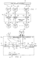
- FIGURE 1 shows a multi-processor system supported by a communication network utilizing communication switches in accordance with the present invention.
- Processor nodes 100, 200, 204 are linked to the communication network 70 via communication links 30, 20, 60 which are directly connected to their associated communication switch 700, 702, 704 respectively.
- Sensor suites 82, 84, 86 are also linked to the communication network 70 via communication links 81, 83, 85 which are directly connected to their associated communication switch 700, 702, 704.
- the communication switches 700, 702, 704 are connected to each other in one-directional, closed loop by communication links 701, 703, 705, 706.
- the communication links may be serial, parallel or a combination of serial and parallel data buses.
- Each communication switch is under the direct control of its associated processor node.
- the first communication switch 700 is controlled by the first processor node 100.
- any processor node can be attributed the task of "master processor" for a given time or application.
- the master processor node controls the distribution of tasks among the other processor nodes (slaves) and monitors and directs their progress throughout each phase of operation.
- the control of the communication switch 700, 702, 704 by its associated (host) processor node 100, 200, 204 is responsive to the overall requirement of the system in its then current phase of operation (data acquisition, data processing, or data exchange).
- an individual communication switch is directly controlled by its associated processor node, it is also ultimately controlled by the master processor node which controls the associated (slave) processor node.
- This indirect means of controlling the communication switches by the master processor node allows the orchestration of data communication among nodes without collision problems.
- a token ring communication protocol may be used during implementation during the data exchange phase.
- the invention also contemplates bi-directional data communication between nodes.
- a segmented network through point to point communication with the capability to concurrently transfer different data in different communication segments within the system is suitable for all phases of operation.
- each processor node communicates directly with other processor nodes over serial links which are primarily used for handling communication protocol.
- the transfer of large volumes of data from one processor node to one or more other processor nodes is done over a fast parallel hardware channel.
- the fast parallel hardware channel is essentially a flat ribbon cable with connectors configured in multi-drop mode.
- the processor nodes 100, 200, 204 in Figure 1 are shown linked to a serial link cross bar switch 75 via serial communication links 11, 13, 17 respectively. This illustrates the option of incorporating independent serial control of transmissions over the communication network 70 utilizing the communication switch 700, 702, 704 which is the subject of this invention.
- FIGURE 2 is a block diagram of a preferred embodiment of the communication switch in accordance with the present invention for use in a geographically extensive parallel communication network where signal degradation may be a concern.
- This communication switch is comprised of a plurality of one directional parallel connectors 710, 722, 728, 729, 731; a differential line receiver with common mode output 718; a line driver with common enable 725 and a plurality of analog multiplexer/demultiplexer switches 713, 714, 720, 723.
- the differential line receiver 718 is suitable for use in balanced and unbalanced digital data transmission and permits connection directly to a bus-organized communication network.
- the line receiver 718 depicted in Fig. 2 is preferably a quadruple differential line receiver such as an MC3450 by Texas Instruments which has a three-state common mode output.
- a line driver with common enable is used as the transmitter 725.
- the transmitter 725 depicted in Fig. 2 is preferably a quadruple line driver such as an MC3453 by Texas Instruments.
- the routing switches 713, 714, 720 and 723 depicted in Fig. 2 are preferably dual four-channel analog multiplexer/demultiplexer switches such as CD4052BM/CD4052BC by Texas Instruments.
- This device is a 4-channel multiplexer having two binary control inputs, A and B and an inhibit input.
- the two binary input signals select 1 or 4 pairs of channel to be turned on and connect the differential analog inputs to the differential outputs.
- the preferred embodiment illustrated in Fig. 2 operates within a parallel communication network as described below.
- the communication switch 702 at the direction of its host processor node 200 sets routing switch pair 713 and 714 to position "B" and routing switch 720 to a closed position. If the input data stream 83 originating at the associated sensor suite is to be simultaneously transmitted to other nodes in the processing system, the host processor node 200 will also set routing switch 723 to position "A".
- input data stream 83 is passed by the one directional 32 bit parallel connector 731 to 32-bit parallel data busses 732 and 733, through switch pair 713 and 714, then on 32-bit parallel data busses 715, 716 to the differential input terminals of the receiver 718.
- the differential line receiver 718 converts the differential voltage input to a common-mode output signal which then continues to the host processor node 200 via 32-bit parallel data bus 719, routing switch 720, 32-bit parallel data bus 721 and through one directional output connector 722 and finally 32-bit parallel data bus 20A. No conversion occurs at the input connector 731 and the incoming data stream 83 is also in the form of a differential voltage transmission.
- the host processor node 200 pre-sets routing switch 723 to position "A". This enables the signal on 32-bit parallel data bus to pass through routing switch 723 and 32-bit parallel data bus 724 to line driver 725.
- the line driver 725 amplifies the signal and converts it from common mode input to differential voltage output carried on 32 bit data busses 726 and 727 through the one directional output connector 728 and on 32-bit parallel data line 703 to the up-link communication switch and beyond as required by the processing system application. No conversion occurs at the output connector 728, and the outgoing differential voltage signal carried by 726 and 727 is carried in the same form by 703.
- routing switch pair 713 and 714 to position "A" at the direction of its host processor node 200. If the host processor node 200 is to receive the data being transmitted from an up-link source, routing switch 720 is set to closed position. If the data is to be transmitted to other nodes in the processing system, the host processor node 200 will also set routing switch 723 to position "A".
- data transmitted on 32-bit parallel data bus 701 is passed by the one directional 32 bit parallel connector 710 to 32-bit parallel data busses 711 and 712, through switch pair 713 and 714, then on 32-bit parallel data busses 715, 716 to the differential input terminals of the receiver 718.
- the differential line receiver 718 converts the differential voltage input to a common-mode output signal which then continues to the host processor node 200 via 32-bit parallel data bus 719, routing switch 720, 32-bit parallel data bus 721.
- the signal passes through one directional output connector 722 to 32-bit parallel data bus 20A. No conversion occurs at the input connector 710, and the data transmission signal on 701 is also in the form of a differential voltage transmission.
- the host processor node 200 pre-sets routing switch 723 to position "A".
- the common mode signal on 32-bit parallel data bus 719 then passes through routing switch 723 and 32-bit parallel data bus 724 to line driver 725.
- the line driver 725 amplifies the signal and converts it from common mode input to differential voltage output.
- This output is then carried on 32-bit data busses 726 and 727 as differential voltages through the one directional output connector 728 and on 32-bit parallel data line 703 to the up-link communication switch and beyond as required by the processing system application. No conversion occurs at the output connector 728, and the outgoing differential voltage signal carried by 726 and 727 is carried in the same form by 703.
- the host processor node 200 will set routing switch 723 to position "B" to allow distribution of the data to the adjacent communication switch down link and beyond as required by the application.
- routing switches are disabled or set to "open" position.
- the communication switch design allows a host processor node to receive data while transmitting its own data simultaneously provided that the incoming data is destined only for the host processor node.
- the diagram in Figure 3 illustrates another preferred embodiment of the communication switch for use in a geographically extensive parallel communication network operating in an environment where there is neither concern of signal distortion nor concern of signal degradation over distances between communication switches.
- An example is a communication network operating in a very low noise environment and very short total distance from source to terminal for a given transmission or in a geographically extensive communication network applying optical fiber technology.
- This communication switch is comprised of a plurality of one directional parallel connectors 710, 722, 728, 729, 731 and a plurality of analog multiplexer/demultiplexer switches 713, 714, 720, 723.
- the communication switch of Fig. 3 operates in a manner analogous to that described for the communication switch illustrated in Fig. 2 except that there is neither concern of signal distortion nor concern of signal degradation over distances between communication switches. Therefore, the switch design dispenses with the receiver/driver pair and concentrates on controlling the data paths through the communication switch by setting the routing switches as described above.
- FIGS. 4, 5 and 6 represent the various possible logical settings of the communication switch of the present invention during each phase of the operation of a multi-processor system as described here. Any combination of logical settings may be used as required by a particular application during a given phase of operation.
- any processor node can be attributed the task of "master processor" for a given time or application.
- the master processor node controls the distribution of tasks among the other processor nodes (slaves) and monitors and directs their progress throughout each phase of operation.
- the control of the communication switch 700, 702, 704 by its associated (host) processor node 100, 200, 204 is responsive to the overall requirement of the system in its then current phase of operation (data acquisition, data processing, or data exchange).
- data acquisition, data processing, or data exchange data acquisition, data processing, or data exchange.
- FIGURE 2 shows dashed control lines 1,2,3,4 from a controlling processor to each internal routing switch 713,714,720,723.
- the controlling processor may be a master processor of the multi-processor system, a host node processor associated with that switch, or a processor assigned the task of communication management within the multi-processor system.
- networks utilizing the communication switch transmit within an orchestrated overall system communication plan. When not in use, routing switches are disabled or set to "open" position.
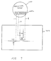
- FIGURE 7 shows another preferred embodiment of the communication switch of the present invention in which a host processor node 200 controls the communication switch 702 through the use of a memory location or register 200a directly connected via control lines 1,2,3 to the internal switches 713, 720, 723 of the communication switch 702. Details of the switch which are not essential to the illustration of the control means are eliminated for simplicity. The illustration of only a few internal switches and the simplified nature of the illustration depicted in FIGURE 7 does not limit the complexity of the communication switch nor its relationship to a processor.
- a preferred method of implementing processor control of the communication switch illustrated in FIGURE 7 is as follows. First, determine the current phase of operation and the need of the host processor node to receive or transmit data. Second, use a look up table or function expression to create a control word. Third, cause the control word to be written to a pre-determined memory location which might be a register which directly controls the control lines of the switches. Finally, effect the functions encoded in the control word via the control lines connected from the register to the switches.
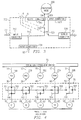
- FIG. 4 a block diagram of the switch of the present invention illustrates the various possible logical settings for the communication switch during the data acquisition phase of the operation of a multi-processor system.
- Figure 4 illustrates the possible variations, it does not limit the sequence nor require use of every logical configuration of the switch.
- communication switch 700 depicts data flowing from the sensor suite exclusively to its host processor node through the communication switch.
- Communication switch 700 is set such that an input data stream 81 from the first sensor suite 82 (or equivalent data stream generator) can flow only to the first processor node 100.
- Communication switch 702 is set such that data originating at second sensor suite 84 may flow to both its associated processor node 200 and other down-link destinations within the multi-processor system.
- Communication switch 708 is set such that data originating at third sensor suite 88 does not flow to its host processor node 202 but rather to other down link destinations within the multi-processor system.
- Communication switch 704 illustrates the situation where the associated sensor suite 86 for the receiving host processor node 204 is either disabled or non-existent and the data to be processed by processor node 204 originated somewhere up-link. Communication switch 704 is set such that data originating up-link is allowed to flow only to processor node 204.
- communication switch 710 is set to allow data originating up-link to flow to both processor node 206 and to other down-link destinations within the multi-processor system. It is also possible to omit data flow to processor node 206 and provide a pass through uplink to downlink coupling.
- FIGURE 5 is a block diagram representing the only logical setting allowed for a communication switch 700, 702, 708, 704 during the discrete data processing phase of the operation of a multi-processor system. Communication flow is disabled in all directions during this phase of operation.
- FIGURE 6 is a block diagram illustrating the various possible logical settings for a communication switch during the data exchange phase of the operation of a multi-processor system.
- Figure 6 illustrates the possible variations but does not limit the sequence nor require use of every logical configuration of the switch.
- Communication switch 700 is set to allow data originating up-link to flow to both processor node 100 and to other down link destinations within the multi-processor system.
- the communication switch design allows a host processor node 100 to receive data from an up-link source while simultaneously transmitting data originating at the host processor node 100 to other down-link destinations within the multi-processor system. This last variation is possible if and only if the incoming data from an up-link source is destined only for the host processor 100 and is not to be passed on to other down-link destinations.
- Communication switch 702 is set such that data originating at its host processor node 702 will flow to destinations down-link.
- Communication switch 708 is set such that data originating at an up-link source is passed through to down-link destinations within the multi-processor system, without being received by the host processor node 202.
- Communication switch 704 is set such that data originating at an up-link source is received only by the host processor node 204.
- FIGURE 8 depicts another preferred embodiment of the communication switch of the present invention coupled with a remotely controlled device.
- a message originating at host processor node 200 is coupled with actuators 744, 745, 746 in a robot device 743 over link 20B to input connector 729.
- the message flows from the connector 729 over data bus 730 through switch 723 set to the "B" position.
- the message then travels over data bus 724 through switch 740 set to the "B" position over data bus 742 through output connector 748 over link 749 which couples to actuators 744, 745, 746.
- Resulting data, if any, are coupled with the input data stream 83 and handled as described in the FIGURE 2 discussion.
- a message originating at an uplink processor node is coupled with the actuators 744, 745, 746 in a robot device 743 over link 701 to input connector 710.
- the message then travels over data buses 711,712 through switches 713, 714 set to the "A" position over data busses 715, 716 through line receiver 718. It continues over data bus 719 through switch 723 set to position "A”.
- the message goes over data bus 724 through switch 740 set to the "B" position over data bus 742 through output connector 748 and over link 749 which couples to actuators 744, 745, 746 with commands.
- Resulting data, if any, are coupled with the input data stream 83 and handled as described in the FIGURE 2 discussion.
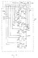
- a buffer/transceiver circuit receives, buffers and retransmits digital data.
- the buffer/transceiver circuits in switch 702 are under control of register 200b in processor node 200.
- the register stores a word or words that determine logic levels of signals on control lines 501, 501a, 502, 502a, 503, 504, 505, 505a, 506, 506a, 507 and 508, which in turn control the buffer/transceiver circuits.
- the width of all control lines are a single bit.
- Each control line is associated with one bit of a word written to register 200b and assumes the value of that bit.
- the control lines are permitted to be multiple bits wide to accommodate, if necessary, circuits chosen to handle the functions of the buffer/transceiver circuits. In this case, the register would then store multiple words for controlling the state of the switch.
- Each buffer/transceiver circuit includes and Enable port (EN) for enabling receiving, buffering and transmission of digital data, as well as a Direction (DIR) port for determining the direction of transmission of the digital data.
- EN Enable port
- DIR Direction
- a buffer/transceiver circuit is enabled for receiving, buffering and transmitting a digital data by presentation of a signal having a predetermined logic level (an enable signal) to its Enable port.
- Control lines 501, 502, 503, 504, 505, 506 and 508 are connected to Enable ports of buffer/transceiver circuits 560, 550, 540, 530, 520, 510 and 570, respectively, and carry Enable signals.
- the direction of transmission is determined by the logic level of a Direction signal on a Direction port: a logic high signal causes the buffer/transceiver circuit to transmit in a first direction; and a logic low signal causes the buffer/transceiver circuit to transmit in a second direction.
- Direction signals are delivered to Direction ports on buffer/transceiver circuits 510, 520, 550, 560 and 570 on, control lines 506a, 505a, 502a, 501a and 507.
- Buffer/transceiver circuits 530 and 540 transmit in only one direction as they handle data flow to and from, respectively, a host processing node.
- the Direction port for buffer/transceiver circuit 530 is tied to a logic high voltage (5 volts), and the Direction port for buffer/transceiver circuit 540 is tied to ground. Because of the control of transmission direction provided by buffer/transceiver circuits, the embodiment of the switch 702 differs from embodiments shown in Figures 1-8 in that it is bi-directional.
- Buffer/transceiver circuits 510 and 520 when enabled, act to receive and transmit data signals outside switch 702, depending on the direction of transmission.
- Buffer/transceiver circuit 510 is coupled to data line 701 and to internal data line 580. In a first direction, it receives data on data line 701 from an uplink source, buffers it and then transmits it, via data line 511, to internal data line 580. In the other direction, it receives and buffers data on internal data line 580 and transmits it to an uplink destination.
- buffer/transceiver circuit 520 receives and buffers data from a sensor suite 84 (Fig.
- Buffer/transceiver circuit 530 when enabled by an appropriate signal on control line 504, acts to transmit data signals outside the switch 702 on line 20a to a host processor (not shown). Through data line 531, buffer/transceiver circuit 530 receives and buffers data carried by signals on internal data line 580. Only one of the two buffer/transceiver circuits 510 and 520 is enabled at time to transmit on internal data line 580, while the remaining two buffer/transceivers on internal data line 580 receive data if they are enabled and their transmission direction is on a data line outside of the switch 702.
- Buffer/transceiver circuit 540 acts to receive data from a host processor node with signals on data line 20b. It then buffers the data and transmits, via data line 541, on internal data line 590.
- Buffer/transceiver circuits 550 and 560 are coupled by, respectively, internal data lines 551 and 561 to internal data line 590.
- the buffer/transceiver circuits 550 and 560 are also coupled to external data lines 749 and 703, respectively.
- buffer/transceiver circuit 550 receives and buffers data on internal data line 590 and transmits it on line 749 to an actuator. In the other direction, data is transmitted from the actuator on data line 749 and transmits it on internal data bus 590.
- buffer/transceiver circuit 560 receives and buffers data on internal data line 590 and transmits it to a downlink destination on line 703 in the first direction. In the other direction, it receives data from the downlink source on line 703 and transmits on internal data line 590. Only one of the buffer/transceiver circuits 540, 550 and 560 is permitted or enabled to transmit on the internal data line 590 at any given time. The other two may receive and buffer data on internal data line 590 and transmit it to an external data line.
- Internal data lines 580 and 590 are coupled through buffer/transceiver circuit 570.
- the buffer/transceiver circuit 570 When enabled by an enabling signal on control line 508, the buffer/transceiver circuit 570 receives and buffers data on one of the two internal data lines 580 and 550 and transmits it on the other of the two lines. The direction of transmission is determined by the logic level of the signal on the Direction port of the buffer/transceiver circuit, as indicated in the figure.
- buffer/transceiver 570 is not enabled, a host processor node on data line 20a is permitted to receive data from an uplink source on data line 701 or from a sensor on line 83 through internal data line 580, and to transmit to a robot on line 749 or to a downlink destination on line 703 through internal data line 590.
- buffer/transceiver circuit 570 When buffer/transceiver circuit 570 is enabled, only one of the buffer/transceiver circuits 510, 520, 540, 550 and 560 is enabled for transmitting data on internal data line 580 or 590.
- data from an uplink source on data line 701 or from a sensor on data line 83 may be transmitted through the other buffer/transceiver circuits, to one or more of the following: downlink destination on data line 703; a robot or actuator on line 749; to an uplink destination on line 701 (if data is originating from a sensor on data line 83), to a sensor on line 83 (if data is originating from an uplink source on line 701) or a host processor on data line 20a.
- Reversing direction of transmission of buffer/transceiver circuit 570 allows data received from an actuator on data line 740 or from a downlink source on line 703 to be transmitted to on or more of the following: an uplink destination on line 701; a sensor on data line 83; a host processor on data line 20a; an actuator on data line 740 (if originating from a downlink source); or a downlink destination data line 703 (if originating from an actuator on data line 740.
- the host processor it is also possible for the host processor to transmit data to the switch on line 20b and to receive that data on line 20a for diagnostic purposes.
- Each buffer/transceiver circuit is preferably implemented using commercially available integrated circuits in order to reduce cost and improve ease of manufacture and service.
- An example of a suitable integrated buffer/transceiver circuit is designated 74ALS245 and manufactured by Texas Instruments, Inc. of Dallas, Texas. Each integrated circuit is 8-bits wide and has an operational frequency of 250 MHz. Data lines 511, 521, 531, 541, 551, 561, 580, 590, 701, 83, 703, 20a, 20b and 749 are 32 bit parallel data buses. Consequently, four 74ALS245 chips are required to implement each buffer/transceiver circuit 510, 520, 530, 540, 550, 560 and 570. The system is not limited, however, to any particular bandwidth.
- Suitable integrated buffer/transceiver circuits are 74F245 (operating at 250 MHz) and 74ABT245 (operating at 344 MHz) manufactured by Signetics/Phillips of Sunnyvale, California. Furthermore, it is permissible though not desirable to have the functions of the integrated buffer/transceiver circuits handled by discrete receiving, buffering and transmitting circuits.
Abstract
Description
- This invention was made with Government support under contract No. DE-AC02-89ER40486 between Universities Research Association, Inc. and the Department of Energy. The Government has certain rights in this invention.
- The present invention relates in general to a high speed switch for either serial, parallel or hybrid networks with minimal protocol required to effectuate random burst transmissions of high density data. In particular, it relates to path control and amplification of signals by communication switches for messages being routed in a serial, parallel or hybrid communication network in the context of multi-processor systems or parallel processing systems with discrete data acquisition, data processing, and data exchange phases of operation.
- Large data processing applications are often partitioned such that they may be carried out by concurrently operating (parallel) processors, each of which handles a different portion of the problem. Independent of the complexity of the processing application, some data communication networks are challenging due to extensive geographic distribution of the elements supported by that communication network and the density of the data transmitted. In either of these two situations or their combination, efficient communication depends on the ability of the communication network to quickly route data from or to elements supported by the communication network. Speed must be maximized, especially in multi-processing systems having heavy traffic due to data acquisition and exchange, while data integrity and simplicity of transmission to any node, from the user's point of view, are maintained.
- Prior art solutions called for a large software processing overhead to parse and interpret communication protocol and message routing at each node of the communication network. These prior art solutions have tended to trade speed in favor of flexibility. Examples of such prior art include the Scalable Coherent Interface (SCI), High Performance Parallel Interface (HIPPI), and Fiber Distributed Data Interface (FDDI).
- The SCI approach transfers communication control words, destination addresses and source address, in addition to data in each 80 word communication packet. This imposes a burden of approximately 25% of the available packet space to communication protocol overhead (16 words), and time is spent parsing and interpreting every transmission.
- The HIPPI is a simplex high performance communication interface which can transmit 800-1600 Megabits per second over a distance of 25 meters using copper cables. In the HIPPI approach, control lines are combined with data lines limiting the network topography to a static communication network configuration, making the HIPPI approach suitable only for parallel and distributed processing systems which have a static distribution of tasks.
- The FDDI is a local area network based on token ring protocol. Information is transferred at the rate of 100 Megabits per second on the FDDI ring in frames that are variable in length. The FDDI provides a bridge between conventional high speed ethernet and high speed fiber optic link. It works such that a backbone FDDI ring connects a local island of ethernet work-group to a similar island located in another part of the network. The FDDI approach requires that control lines, source address, destination addresses, and data travel on the same physical line, thereby imposing burdens similar to the message space and processing time dedicated to communication protocol by the SCI approach and the limitation of a fixed communication network configuration as in the HIPPI approach.
- Crossbar switches have also been commercially available for interconnecting general purpose processing nodes. Crossbar switches have a fixed number of input/output ports. A crossbar switch may be programmed such that a message transmitted through the crossbar switch may be coupled from any input port to any specified output port. The limited number of nodes attachable to a single crossbar switch results in a high cost per channel when crossbar switches are applied to a geographically extensive multi-processor system consisting of a large number of parallel processors.
- These approaches are unsatisfactory for providing efficient data communication in a geographically extensive multi-processor system. It is preferable for such a system to have the following features. It is preferable that the communication network provide simple node access, from the user's perspective, in a reconfigurable multi-processor system. The communication network should also preferably provide intrinsic flexibility to use any combination of the following: (a) multi drop, flat ribbon cable type communication link for short distances, (b) conventional copper (or similar) cable links with intermediary signal filter/amplifiers between start and end points of data transmission as required to prevent signal degradation and distortion if operating over long distances or in a high electromagnetic noise environment, (c) fiber optic links, (d) segmented point to point communication with the capability to concurrently transfer different data in different communication segments within the system, (e) serial data links, (f) parallel data links, or (g) a combination of any of the above approaches applied to individual communication network subsets within the multi-processor system communication network.
- It is also preferable that the communication network provide the highest possible ratio of data transferred to transmission protocol overhead. It is preferred that the communication network facilitate SCI, HIPPI and FDDI interfaces, to other systems. The communication network should also preferably facilitate designer selection of the best type of connection and length for each segment within the communication network and interface(s) with other processing systems in accordance with the requirements of the specific application.
- In sum, prior art communication schemes do not satisfactory provide for a high speed, minimal protocol overhead means for efficiently communicating a random burst of high density data within a geographically extensive multi-processor system during data acquisition/exchange modes of operation. A communication system design is needed which maximizes data routing speed while maintaining data integrity.
- The present invention includes a processor controlled switching device that simplifies node access in a reconfigurable multi-processor system. It provides for efficient data transfer over the communication network with software protocol handled directly by processors over a separate communication network in support of the multi-processor system.
- As an example, a complex multi-processor system supported by a communication network may include the following elements or any combination thereof: sensors, data storage or management devices, actuators, robots, remotely controlled instruments, processing nodes, communication processors, RISC processors, digital signal processors (DSP), transputers, computers, vector processors, or other devices. Such a system may operate in the following modes: initialization, data acquisition, data processing and data exchange. During an "Initialization Phase" each element in the system responds to control messages initiated by the master processor of the multi-processor system transmitted either directly or through subsequent re-transmission or interpretation by intermediary elements. During a "Data Acquisition Phase" each target processing node or data storage device is dedicated to the assimilation of the input data stream originating at the sensors or other data source as tasked by the master processor. During a "Data Processing Phase" each processing node is dedicated to the execution of its processing task as assigned by the master processor. During a "Data Exchange Phase", processing nodes send data to or receive data from other nodes in the parallel processing system for post-processing. Where a data processing system requires that the data acquired during a Data Acquisition Phase be reorganized (redistributed) within the system, a Data Exchange Phase may precede a Data Processing Phase.
- A switching device according to the present invention maximizes data routing speed while maintaining data integrity in a geographically extensive communication network. The invention accomplishes this through the reduction of communication protocol overhead and the amplification of signals which would otherwise be lost due to signal degradation when transmitted long distances over copper wire cables.
- In a preferred embodiment, the communication switch is comprised of several unidirectional parallel connectors, a receiver, a transmitter, and several routing switches. The connectors directly link the communication switch to its immediate neighbors in the communication network, which may comprise any of the system elements listed in the above example multi-processor system. A processor node includes a processor of some type suitable for the particular application of a processing system (e.g., computer, transputer, RISC, DSP, vector processor). A processor node may also include any of various types of memory, data storage/retrieval devices, display terminals or other devices common to scientific or business data processing applications.
- Sensor suites, comprised of one or more sensors, may originate the raw input data streams which drive the processing system. The sensor suites may be geographically fixed or associated with mobile robots controlled by actuators. The sensor types, if any, would be selected in accordance with the particular application (e.g., photo multiplier, photo triode, wire chamber, drift chamber, heat sensors, motion sensors, pattern recognition sensors, voice sensors, radiowave sensors, microwave sensors, radiation sensors, and so forth). Data storage devices are dedicated mass storage devices or data base storage and management systems which may act as global data storage devices for the multi-processor system. Actuators, robots or other remotely controlled instruments which may form part of the system are treated in a manner analogous to both data storage devices and sensors combined in that they must be able to receive command data from the processor nodes and may have to report findings to one or more processor nodes.
- The position of the internal routing switches of each communication switch is under the control of its host processor node. The host processing node sets the internal routing switches of the communication switch in accordance with the current operating phase of the processing system (data acquisition, data processing, or data exchange). The internal routing switches of each communication switch may be set to achieve any one of the following routing configurations: to allow a processor node to receive an input data stream from its associated sensor or equivalent input data stream generator, to allow broadcast of the input data stream originating at one sensor suite to all processor nodes in the processing system, to allow broadcast of the input data stream originating at one sensor suite to selected processor nodes in the processing system, to allow concurrent transmission of the input data stream from each sensor suite to its host processing node, to allow transmission of pre-processed data from one processor node to an adjacent processor node, to allow transmission of pre-processed data from one processor node to a non-adjacent processor node (s), to allow pass through of data not intended for receipt by the host processor, or to allow transmission of pre-processed data from one processor to all other processor nodes in the processing system.
- The receiver and transmitter pair in each communication switch act to refresh each signal being transmitted over the communication network. The integrity of the signal (data transmission) which might otherwise have been lost or become unreliable due to signal transmission degradation over some limiting distance, is preserved in the network through amplification of the signal as it passes through each communication switch. The receiver and transmitter pair may be omitted if there is no anticipated signal degradation because the transmission is being effected over optical line or the distance actually traversed by the signal does not exceed the limit if the cable medium (eg., 25 meters for copper wire).
- A communication switch according to the present invention is, for example, ideally suited for use in a high energy physics experiment test bed which requires simultaneous data acquisition from all sensors for processing by parallel processors in the test bed. In addition to data acquisition, a switch according to the invention is also suited for use in systems exchanging large amounts of data between system elements in real-time, such as in real-time robotic applications and real-time image processing applications. Furthermore, a communication switch according to the present invention is suited for use in complex real-time simulations and replays such as war games where terrain, atmospheric conditions, resource deployment and movements, countermeasures, engagements, communication nets, and several other theater elements are simultaneously varied through the application of multiple input data streams and human interaction.
- For a more complete understanding of the present invention, and for further details and advantages thereof, reference is now made to the following Detailed Description taken in conjunction with the accompanying drawings, in which:
- FIGURE 1 is a block diagram of a multi-processor system supported by a communication network utilizing a preferred embodiment of communication switches according to the present invention.
- FIGURE 2 is a block diagram of a preferred embodiment of a communication switch according to the present invention for use in a communication network where signal degradation is a concern.
- FIGURE 3 is a block diagram of another preferred embodiment of a communication switch for use in a communication network where signal degradation is not a constraint.
- FIGURE 4 is a block diagram representing the various possible logical settings for the communication switch of the present invention during the Data Acquisition phase of a multi-processor system's operation.
- FIGURE 5 is a block diagram representing the various possible logical settings for the communication switch of the present invention during the Data Processing phase of the operation of a multi-processor system.
- FIGURE 6 is a block diagram representing the various possible logical settings for the communication switch during the Data Exchange phase of the operation of a multi-processor system.
- FIGURE 7 is a block diagram showing another preferred embodiment of a communication switch of the present invention under processor control.
- FIGURE 8 is a block diagram showing another preferred embodiment of the communication switch of the present invention which includes coupling with a remotely controlled device.
- FIGURE 9 is block diagram of another preferred embodiment for the communications switch depicted in Figure 8.
- The present invention relates to a method and apparatus for path control and amplification of signals being routed in a serial or a parallel communication network.
- FIGURE 1 shows a multi-processor system supported by a communication network utilizing communication switches in accordance with the present invention.
Processor nodes communication network 70 viacommunication links communication switch Sensor suites communication network 70 viacommunication links communication switch communication links - Each communication switch is under the direct control of its associated processor node. For example, the
first communication switch 700 is controlled by thefirst processor node 100. In a concurrent parallel processing system or distributed processing system with discrete phases of operation, for a given topology, any processor node can be attributed the task of "master processor" for a given time or application. The master processor node controls the distribution of tasks among the other processor nodes (slaves) and monitors and directs their progress throughout each phase of operation. The control of thecommunication switch processor node - This indirect means of controlling the communication switches by the master processor node allows the orchestration of data communication among nodes without collision problems. A token ring communication protocol may be used during implementation during the data exchange phase. However, the invention also contemplates bi-directional data communication between nodes. A segmented network through point to point communication with the capability to concurrently transfer different data in different communication segments within the system is suitable for all phases of operation.
- The speed of data transfer within the system may be further improved through the separation of data transmission packets and their control in a manner similar to that taught in U.S. patent application Serial No. 07/1856622, filed on March 24, 1992 by Crosetto entitled "Parallel Data Transfer Network Controlled by a Dynamically Re-Configurable Serial Network", which is incorporated herein by reference. In that communication arrangement, each processor node communicates directly with other processor nodes over serial links which are primarily used for handling communication protocol. The transfer of large volumes of data from one processor node to one or more other processor nodes is done over a fast parallel hardware channel. The fast parallel hardware channel is essentially a flat ribbon cable with connectors configured in multi-drop mode.
- The
processor nodes cross bar switch 75 via serial communication links 11, 13, 17 respectively. This illustrates the option of incorporating independent serial control of transmissions over thecommunication network 70 utilizing thecommunication switch - The use of short control messages over direct, transputer to transputer, serial communication links to effect communication protocol for the transmission of large volumes of data between parallel processing nodes, is made easier for the designer by the availability of an operating system such as OCCAM on a transputer. Using a serial communication network to control the transmission of large volumes of data over a parallel communication network reduces the software protocol required to parse and interpret each message and increases the "pay load" for each transmission over the parallel communication network. The above approach, when combined with this invention, will increase the flexibility of the multi-processor system with respect to dynamic topographical reconfigurability while maintaining optimal transmission speed and data integrity.
- FIGURE 2 is a block diagram of a preferred embodiment of the communication switch in accordance with the present invention for use in a geographically extensive parallel communication network where signal degradation may be a concern. This communication switch is comprised of a plurality of one directional
parallel connectors common mode output 718; a line driver with common enable 725 and a plurality of analog multiplexer/demultiplexer switches 713, 714, 720, 723. - The
differential line receiver 718 is suitable for use in balanced and unbalanced digital data transmission and permits connection directly to a bus-organized communication network. Theline receiver 718 depicted in Fig. 2 is preferably a quadruple differential line receiver such as an MC3450 by Texas Instruments which has a three-state common mode output. - A line driver with common enable is used as the
transmitter 725. When the enable input is high, a constant output current is switched between each pair of output terminals in response to the logic level at the input of that channel. When the enable is low, all channel outputs are nonconductive. This minimizes loading in part-time communication networks where a large number of drivers share the same line. Thetransmitter 725 depicted in Fig. 2 is preferably a quadruple line driver such as an MC3453 by Texas Instruments. - The routing switches 713, 714, 720 and 723 depicted in Fig. 2 are preferably dual four-channel analog multiplexer/demultiplexer switches such as CD4052BM/CD4052BC by Texas Instruments. This device is a 4-channel multiplexer having two binary control inputs, A and B and an inhibit input. The two binary input signals select 1 or 4 pairs of channel to be turned on and connect the differential analog inputs to the differential outputs. When a logical "1" is present at the inhibit input terminal all channels are "OFF". The preferred embodiment illustrated in Fig. 2 operates within a parallel communication network as described below.
- During the data acquisition phase of operation, the
communication switch 702 at the direction of itshost processor node 200 sets routingswitch pair routing switch 720 to a closed position. If theinput data stream 83 originating at the associated sensor suite is to be simultaneously transmitted to other nodes in the processing system, thehost processor node 200 will also setrouting switch 723 to position "A". - After the
communication switch 702 is prepared for the receipt and routing of data as described above,input data stream 83 is passed by the one directional 32 bitparallel connector 731 to 32-bit parallel data busses 732 and 733, throughswitch pair receiver 718. Thedifferential line receiver 718 converts the differential voltage input to a common-mode output signal which then continues to thehost processor node 200 via 32-bitparallel data bus 719, routingswitch 720, 32-bitparallel data bus 721 and through onedirectional output connector 722 and finally 32-bitparallel data bus 20A. No conversion occurs at theinput connector 731 and theincoming data stream 83 is also in the form of a differential voltage transmission. - If the
input data stream 83 originating at the associated sensor suite is to be simultaneously transmitted to other nodes in the processing system, thehost processor node 200pre-sets routing switch 723 to position "A". This enables the signal on 32-bit parallel data bus to pass throughrouting switch 723 and 32-bitparallel data bus 724 toline driver 725. Theline driver 725 amplifies the signal and converts it from common mode input to differential voltage output carried on 32 bit data busses 726 and 727 through the onedirectional output connector 728 and on 32-bitparallel data line 703 to the up-link communication switch and beyond as required by the processing system application. No conversion occurs at theoutput connector 728, and the outgoing differential voltage signal carried by 726 and 727 is carried in the same form by 703. - During the data exchange phase of operation, if the data being transmitted to the
communication switch 702 originates at an up-link source, thecommunication switch 702 will set routingswitch pair host processor node 200. If thehost processor node 200 is to receive the data being transmitted from an up-link source, routingswitch 720 is set to closed position. If the data is to be transmitted to other nodes in the processing system, thehost processor node 200 will also setrouting switch 723 to position "A". - After the
communication switch 702 is prepared for the receipt and routing of data as described above, data transmitted on 32-bitparallel data bus 701 is passed by the one directional 32 bitparallel connector 710 to 32-bit parallel data busses 711 and 712, throughswitch pair receiver 718. Thedifferential line receiver 718 converts the differential voltage input to a common-mode output signal which then continues to thehost processor node 200 via 32-bitparallel data bus 719, routingswitch 720, 32-bitparallel data bus 721. The signal passes through onedirectional output connector 722 to 32-bitparallel data bus 20A. No conversion occurs at theinput connector 710, and the data transmission signal on 701 is also in the form of a differential voltage transmission. - If the data originating at an up-link source is to be simultaneously transmitted to other nodes in the processing system, the
host processor node 200pre-sets routing switch 723 to position "A". The common mode signal on 32-bitparallel data bus 719 then passes throughrouting switch 723 and 32-bitparallel data bus 724 toline driver 725. Theline driver 725 amplifies the signal and converts it from common mode input to differential voltage output. This output is then carried on 32-bit data busses 726 and 727 as differential voltages through the onedirectional output connector 728 and on 32-bitparallel data line 703 to the up-link communication switch and beyond as required by the processing system application. No conversion occurs at theoutput connector 728, and the outgoing differential voltage signal carried by 726 and 727 is carried in the same form by 703. - If the data to be transmitted originates at the
host processor node 200, thehost processor node 200 will set routingswitch 723 to position "B" to allow distribution of the data to the adjacent communication switch down link and beyond as required by the application. - When not in use, routing switches are disabled or set to "open" position. The communication switch design allows a host processor node to receive data while transmitting its own data simultaneously provided that the incoming data is destined only for the host processor node.
- The diagram in Figure 3 illustrates another preferred embodiment of the communication switch for use in a geographically extensive parallel communication network operating in an environment where there is neither concern of signal distortion nor concern of signal degradation over distances between communication switches. An example is a communication network operating in a very low noise environment and very short total distance from source to terminal for a given transmission or in a geographically extensive communication network applying optical fiber technology. This communication switch is comprised of a plurality of one directional
parallel connectors - The communication switch of Fig. 3 operates in a manner analogous to that described for the communication switch illustrated in Fig. 2 except that there is neither concern of signal distortion nor concern of signal degradation over distances between communication switches. Therefore, the switch design dispenses with the receiver/driver pair and concentrates on controlling the data paths through the communication switch by setting the routing switches as described above.
- Note that preferred embodiments illustrated in Figures 2 and 3 lend themselves equally well to serial communication network applications with minor changes in the connectors and communication links.
- The block diagrams of Figures 4, 5 and 6 represent the various possible logical settings of the communication switch of the present invention during each phase of the operation of a multi-processor system as described here. Any combination of logical settings may be used as required by a particular application during a given phase of operation. In a concurrent parallel processing system or distributed processing system with discrete phases of operation, for a given topology, any processor node can be attributed the task of "master processor" for a given time or application. The master processor node controls the distribution of tasks among the other processor nodes (slaves) and monitors and directs their progress throughout each phase of operation. The control of the
communication switch processor node - This indirect means of controlling the communication switches by the master processor node allows the orchestration of data communication among nodes without collision problems. A processor controls the position of the internal routing switches contained in its associated communication switch. FIGURE 2 shows dashed
control lines - FIGURE 7 shows another preferred embodiment of the communication switch of the present invention in which a
host processor node 200 controls thecommunication switch 702 through the use of a memory location or register 200a directly connected viacontrol lines internal switches communication switch 702. Details of the switch which are not essential to the illustration of the control means are eliminated for simplicity. The illustration of only a few internal switches and the simplified nature of the illustration depicted in FIGURE 7 does not limit the complexity of the communication switch nor its relationship to a processor. - A preferred method of implementing processor control of the communication switch illustrated in FIGURE 7 is as follows. First, determine the current phase of operation and the need of the host processor node to receive or transmit data. Second, use a look up table or function expression to create a control word. Third, cause the control word to be written to a pre-determined memory location which might be a register which directly controls the control lines of the switches. Finally, effect the functions encoded in the control word via the control lines connected from the register to the switches.
- Referring again to Figure 4, a block diagram of the switch of the present invention illustrates the various possible logical settings for the communication switch during the data acquisition phase of the operation of a multi-processor system. Although Figure 4 illustrates the possible variations, it does not limit the sequence nor require use of every logical configuration of the switch.
- The most common of the possible logical settings for the communication switch is illustrated in by
communication switch 700 which depicts data flowing from the sensor suite exclusively to its host processor node through the communication switch.Communication switch 700 is set such that aninput data stream 81 from the first sensor suite 82 (or equivalent data stream generator) can flow only to thefirst processor node 100. -
Communication switch 702 is set such that data originating atsecond sensor suite 84 may flow to both its associatedprocessor node 200 and other down-link destinations within the multi-processor system. -
Communication switch 708 is set such that data originating atthird sensor suite 88 does not flow to itshost processor node 202 but rather to other down link destinations within the multi-processor system. -
Communication switch 704 illustrates the situation where the associatedsensor suite 86 for the receivinghost processor node 204 is either disabled or non-existent and the data to be processed byprocessor node 204 originated somewhere up-link.Communication switch 704 is set such that data originating up-link is allowed to flow only toprocessor node 204. - In a similar situation,
communication switch 710 is set to allow data originating up-link to flow to bothprocessor node 206 and to other down-link destinations within the multi-processor system. It is also possible to omit data flow toprocessor node 206 and provide a pass through uplink to downlink coupling. - FIGURE 5 is a block diagram representing the only logical setting allowed for a
communication switch - Some applications of parallel processing require iterative intermediate data processing and data exchange phases of operation prior to overall task completion. In such applications the communication switches logical state will alternate between one or more of the states depicted in Figure 6 (data exchange phase) and the state depicted in Figure 5 (data processing phase).
- FIGURE 6 is a block diagram illustrating the various possible logical settings for a communication switch during the data exchange phase of the operation of a multi-processor system. Figure 6 illustrates the possible variations but does not limit the sequence nor require use of every logical configuration of the switch.
-
Communication switch 700 is set to allow data originating up-link to flow to bothprocessor node 100 and to other down link destinations within the multi-processor system. The communication switch design allows ahost processor node 100 to receive data from an up-link source while simultaneously transmitting data originating at thehost processor node 100 to other down-link destinations within the multi-processor system. This last variation is possible if and only if the incoming data from an up-link source is destined only for thehost processor 100 and is not to be passed on to other down-link destinations. -
Communication switch 702 is set such that data originating at itshost processor node 702 will flow to destinations down-link.Communication switch 708 is set such that data originating at an up-link source is passed through to down-link destinations within the multi-processor system, without being received by thehost processor node 202.Communication switch 704 is set such that data originating at an up-link source is received only by thehost processor node 204. - FIGURE 8 depicts another preferred embodiment of the communication switch of the present invention coupled with a remotely controlled device. A message originating at
host processor node 200 is coupled withactuators robot device 743 over link 20B to inputconnector 729. The message flows from theconnector 729 overdata bus 730 throughswitch 723 set to the "B" position. The message then travels overdata bus 724 throughswitch 740 set to the "B" position over data bus 742 throughoutput connector 748 over link 749 which couples toactuators input data stream 83 and handled as described in the FIGURE 2 discussion. - A message originating at an uplink processor node is coupled with the
actuators robot device 743 overlink 701 to inputconnector 710. The message then travels over data buses 711,712 throughswitches line receiver 718. It continues overdata bus 719 throughswitch 723 set to position "A". The message goes overdata bus 724 throughswitch 740 set to the "B" position over data bus 742 throughoutput connector 748 and over link 749 which couples toactuators input data stream 83 and handled as described in the FIGURE 2 discussion. - Referring now to FIGURE 9, shown is another preferred implementation of
switch 702, using buffer/transceiver circuits switch 702 are under control of register 200b inprocessor node 200. The register stores a word or words that determine logic levels of signals oncontrol lines - Each buffer/transceiver circuit includes and Enable port (EN) for enabling receiving, buffering and transmission of digital data, as well as a Direction (DIR) port for determining the direction of transmission of the digital data. A buffer/transceiver circuit is enabled for receiving, buffering and transmitting a digital data by presentation of a signal having a predetermined logic level (an enable signal) to its Enable port.
Control lines transceiver circuits transceiver circuits 510, 520, 550, 560 and 570 on,control lines transceiver circuits transceiver circuit 530 is tied to a logic high voltage (5 volts), and the Direction port for buffer/transceiver circuit 540 is tied to ground. Because of the control of transmission direction provided by buffer/transceiver circuits, the embodiment of theswitch 702 differs from embodiments shown in Figures 1-8 in that it is bi-directional. - Buffer/
transceiver circuits 510 and 520, when enabled, act to receive and transmit data signals outsideswitch 702, depending on the direction of transmission. Buffer/transceiver circuit 510 is coupled todata line 701 and to internal data line 580. In a first direction, it receives data ondata line 701 from an uplink source, buffers it and then transmits it, via data line 511, to internal data line 580. In the other direction, it receives and buffers data on internal data line 580 and transmits it to an uplink destination. Similarly, when enabled and operating in the first direction, buffer/transceiver circuit 520 receives and buffers data from a sensor suite 84 (Fig. 1) carried by a signal ondata line 83 and transmits it, viadata line 521, to internal data line 580. In the other direction, data is transmitted to sensors vialine 83. Buffer/transceiver circuit 530, when enabled by an appropriate signal oncontrol line 504, acts to transmit data signals outside theswitch 702 on line 20a to a host processor (not shown). Throughdata line 531, buffer/transceiver circuit 530 receives and buffers data carried by signals on internal data line 580. Only one of the two buffer/transceiver circuits 510 and 520 is enabled at time to transmit on internal data line 580, while the remaining two buffer/transceivers on internal data line 580 receive data if they are enabled and their transmission direction is on a data line outside of theswitch 702. - Buffer/
transceiver circuit 540 acts to receive data from a host processor node with signals on data line 20b. It then buffers the data and transmits, viadata line 541, oninternal data line 590. Buffer/transceiver circuits 550 and 560 are coupled by, respectively,internal data lines internal data line 590. The buffer/transceiver circuits 550 and 560 are also coupled toexternal data lines 749 and 703, respectively. In a first direction, buffer/transceiver circuit 550 receives and buffers data oninternal data line 590 and transmits it on line 749 to an actuator. In the other direction, data is transmitted from the actuator on data line 749 and transmits it oninternal data bus 590. Similarly, buffer/transceiver circuit 560 receives and buffers data oninternal data line 590 and transmits it to a downlink destination online 703 in the first direction. In the other direction, it receives data from the downlink source online 703 and transmits oninternal data line 590. Only one of the buffer/transceiver circuits 540, 550 and 560 is permitted or enabled to transmit on theinternal data line 590 at any given time. The other two may receive and buffer data oninternal data line 590 and transmit it to an external data line. -
Internal data lines 580 and 590 are coupled through buffer/transceiver circuit 570. When enabled by an enabling signal oncontrol line 508, the buffer/transceiver circuit 570 receives and buffers data on one of the two internal data lines 580 and 550 and transmits it on the other of the two lines. The direction of transmission is determined by the logic level of the signal on the Direction port of the buffer/transceiver circuit, as indicated in the figure. When buffer/transceiver 570 is not enabled, a host processor node on data line 20a is permitted to receive data from an uplink source ondata line 701 or from a sensor online 83 through internal data line 580, and to transmit to a robot on line 749 or to a downlink destination online 703 throughinternal data line 590. - When buffer/transceiver circuit 570 is enabled, only one of the buffer/
transceiver circuits internal data line 580 or 590. When the logic level of the direction signal oncontrol line 507 is high, data from an uplink source ondata line 701 or from a sensor ondata line 83 may be transmitted through the other buffer/transceiver circuits, to one or more of the following: downlink destination ondata line 703; a robot or actuator on line 749; to an uplink destination on line 701 (if data is originating from a sensor on data line 83), to a sensor on line 83 (if data is originating from an uplink source on line 701) or a host processor on data line 20a. Reversing direction of transmission of buffer/transceiver circuit 570 allows data received from an actuator ondata line 740 or from a downlink source online 703 to be transmitted to on or more of the following: an uplink destination online 701; a sensor ondata line 83; a host processor on data line 20a; an actuator on data line 740 (if originating from a downlink source); or a downlink destination data line 703 (if originating from an actuator ondata line 740. In this direction, it is also possible for the host processor to transmit data to the switch on line 20b and to receive that data on line 20a for diagnostic purposes. - Each buffer/transceiver circuit is preferably implemented using commercially available integrated circuits in order to reduce cost and improve ease of manufacture and service. An example of a suitable integrated buffer/transceiver circuit is designated 74ALS245 and manufactured by Texas Instruments, Inc. of Dallas, Texas. Each integrated circuit is 8-bits wide and has an operational frequency of 250 MHz.
Data lines transceiver circuit - Although preferred embodiments of the invention have been described in the foregoing Detailed Description and illustrated in the accompanying drawings, it will be understood that the invention is not limited to the embodiments disclosed, but is capable of numerous rearrangements, modifications, and substitutions of parts and elements without departing from the spirit of the invention. Accordingly, the present invention is intended to encompass such rearrangements, modifications, and substitutions of parts and elements as fall within the scope of the invention.
Claims (28)
- A communications switch for high speed transmission of random bursts of high density data with low protocol overhead for use in a communication network supporting a geographically extensive multi-processor system and having a dynamically reconfigurable topology, comprising:
first switch means for coupling for high speed transmission of a data stream a first communication link carrying a data stream from an uplink source to a host processor node, the first switch means in response to a first control signal from the multi-processor system;
second switch means for coupling for high speed transmission of a data stream the host processor to a second communication link for carrying a data stream to a downlink destination, the second switch means responsive to a second control signal from the multi-processor system; and
third switch means for coupling for high speed transmission of a data stream the first communication link to the second communication link for carrying a data stream from an uplink source to a downlink destination, the third switch means responsive to a third control signal from the multi-processor system. - The switch of Claim 1 further comprising fourth switch means for coupling for high speed transmission of a data stream a data source associated with the communications switch to a host processor node, the fourth switch means responsive to a fourth control signal from the multi-processor system.
- The switch of Claim 1 further comprising fifth switch means for coupling for high speed transmission of a data stream a host processor to an actuator associated with the communications switch, the fifth switch means responsive to a fifth control signal from the multi-processor system.
- The switch of Claim 1 further comprising sixth switch means for coupling for high speed transmission of a data flow an uplink processor to a actuator associated with the communications switch, the sixth switch means responsive to a sixth control signal from the multi-processor system.
- The switch of Claim 1 further comprising seventh switch means for coupling for high speed transmission of data a data source associated with the communications switch to the second communication link for carrying a data flow from the data source to a downlink processor node, the seventh switch means responsive to a seventh control signal from the multi-processor system.
- The switch of Claim 1 further comprising an amplifier for refreshing a data stream coupled by the switch to a downlink destination.
- A switch for high speed transmission of random bursts of high density data with low protocol overhead in a data communication network supporting a geographically extensive multi-processor system the system having a plurality of processor nodes, a processor node being associated with a switch, the switch comprising:
first switch means, responsive to a first command signal from a processor node, for selectively coupling an input data stream from a data source associated with the switch to a processor node associated with the switch during a discrete data acquisition phase of the multi-processor system;
second switch means, responsive to a second command signal from the processor node, for selectively disabling data transmissions through the switch during a discrete data processing phase of the multi-processor system operation; and
third switch means, responsive to a third command signal from the processor node, for selectively coupling communications links to neighboring switches for coupling a flow of data from an uplink processor node to a downlink processor node within the multi-processor system during a data exchange phase of operation of the multi-processor system. - The switch of Claim 7 further comprising fourth switch means, responsive to a fourth command signal from a processor node, for selectively coupling communication links to neighboring switches for communicating an input data stream to a processor node during a discrete data acquisition phase of the multi-processor system operation.
- The switch of Claim 7 further comprising fifth switch means, responsive to a fifth command signal from a processor node, for selectively coupling a communication link coupled to a neighboring switch to an actuator means coupled to the switch for coupling a flow of data from an uplink processing node to the actuator means.
- The switch of Claim 7 wherein the first, second and third command signals are determined by a single master processor node in communication with the first, second and third switch means, wherein the master processor node determines a current phase of operation of the multi-processor system and a requirement of a processor node associated with the switch to receive, pass or transmit data.
- The switch of Claim 10 wherein the master processor node creates a control word representative of a state of the first switch means, the second switch means and the third switch means, and causes the control word to be written to a pre-determined memory location; the memory location being coupled to control lines controlling the state of the first, second and third switch means.
- Switching apparatus controlled by a host processor node for high speed transmission of random bursts of high density data with low protocol overhead for use in a communication network supporting a geographically extensive multi-processor system the system having a plurality of processor nodes, said switch apparatus comprising:
a first input connector;
a second input connector;
a third input connector;
a first output connector;
a second output connector;
a first switch means having an open position, a first closed position and a second closed position;
a second switch means having an open position, a first closed position and a second closed position;
a third switch means having an open position and a closed position; and
control lines from the host processor node to the first, second and third switch means for controlling the positions of said switch means;
wherein said first input connector is coupled to said first output connector when said first switch is in a first closed position and said third switch is in a closed position;
said first input connector is coupled to said second output connector when said first switch is in a first closed position and said second switch is in a first closed position;
said third input connector is coupled to said first output connector when said first switch is in a second closed position and said third switch is in a closed position;
said third input connector is coupled to said second output connector when said first switch is in a second closed position and said second switch is in a first closed position; and
said second input connector is coupled with said second output connector when said second switch is in a second closed position. - The switch apparatus of Claim 12 wherein the states of all said switches are determined by a single master processor in communication with all said switches wherein the master processor:(a) determines a current phase of operation of the multi-processor system and the need of the host processor node to receive, pass or transmit data;(b) uses a look up table or function expression to create a control word;(c) causes the control word to be written to a pre-determined memory location; and(d) effects the functions encoded in the control word via the control lines connected from the memory word bits to the switches causing the switch to respond by opening or closing the switch in the appropriate position.
- The switch of Claim 12 further comprising:
a line receiver and a line driver wherein the input of said line receiver is coupled to the first three-state switch output and the output of said line receiver is coupled to the two-state switch and the first position of the second three-state switch; and
the input of the said line driver is coupled to the second three-state switch and the output of said line driver is coupled to the second output connector. - A method of high speed switching of random bursts of high density data with low protocol overhead for use in a communication network supporting a geographically extensive multi-processor system and having a dynamically reconfigurable topology, the method comprising the steps of:
coupling with a communications switch for high speed transmission of a data stream a first communication link carrying a data stream from an uplink source to a host processor node using a first control signal from the multi-processor system;
coupling with the communications switch for high speed transmission of a data stream the host processor to a second communication link for carrying a data stream to a downlink destination using a second control signal from the multi-processor system; and
coupling with the communications switch for high speed transmission of a data stream the first communication link to the second communication link for carrying a data stream from an uplink source to a downlink destination using a third control signal from the multi-processor system. - The method of Claim 15 further comprising the step of coupling with a the communications switch for high speed transmission of a data flow a data source associated with the communications switch to a host processor node using a fourth control signal from the multi-processor system.
- The method of Claim 15 further comprising the step of coupling with the communications switch for high speed transmission of a data flow a host processor to a remotely controlled device associated with the communications switch using a fifth control signal from the multi-processor system.
- The method of Claim 15 further comprising the step of coupling with the communications switch for high speed transmission of a data flow an uplink processor to a remotely controlled device associated with the communications switch using a sixth control signal from the multi-processor system.
- The method of Claim 15 further comprising the step of refreshing a data stream coupled by the communications switch to a downlink destination.
- A fast data communications network for transferring random bursts of high density data with minimum software overhead in a geographically extensive, multi-processor system having a plurality of processor nodes operating in coordination, the fast data communications network comprising:
first, second and third communications switches;
a first data communications link between the first and second switches, and a second data communications link between the second and third switches;
three processing nodes, each coupled for data communication to one of the three communication switches;
each of the three communication switches adapted to independently assume one of a plurality routing positions for data flow through the switch in response to control signals from the multi-processor system; the plurality of routing positions for data flow including a first routing position for a data flow from one of the two communications link to the processor node associated with the communications switch, a second routing position for a data flow from the processor node associated with the switch to another one of the two other communications switches through one of the two communications links, and a third routing position for a data flow from the first communication link to the second communication link. - The fast data communications network of Claim 20 wherein the plurality of routing positions further includes a fourth routing position for a data flow from the data source to one of the two communications links.
- The fast data communications network of Claim 20 wherein the plurality of routing positions further includes a fifth routing position for a data flow from host processor node to an actuator associated with the host processor node and coupled to the switch, and a sixth routing position for routing a data flow from on one of the two communications links to the actuator.
- The fast data communications network of Claim 20 further including a data source coupled to one of the three communication switches; and wherein the plurality of routing positions further includes a first routing position for a data flow from the data source to the processor node associated with the switch.
- A method of transmitting random bursts of high-density data in a geographically extensive multi-processor system, the multi-processor system acquiring and exchanging data over a high speed communication network and including devices for acquiring data or actuating in response to data; the high speed communications network having a plurality of communication switches wherein each communications switch is linked to at least one neighboring communications switch and to one host processor node, and wherein each device for sensing or actuating is coupled to a communications switch; each communication switch having a the method comprising the steps of:
determining data flow requirements in the high speed communications network for supporting the multi-processor system during a discrete operational phase of the multi-processor system;
configuring with control signals from the multi-processor system each of the plurality of communications switches in the communication system for one of a plurality of data flows through the switch during the discrete phase of operation; the plurality of data flows including no data flow, data flow from one neighboring communication switch to another neighboring communication switch, and data flow from a host processor node to a neighboring communications switch, and data flow from a neighboring communication switch to the host processor node. - The method of Claim 24 wherein the plurality of data flows further includes data flow from a sensor to a host processor node.
- The method of Claim 24 wherein the plurality of data flows further includes data flow from a sensor to a neighboring communications switch.
- The method of Claim 24 wherein the plurality of data flows further includes data flow from a host processor node associated with a communications switch to an actuator coupled to the communications switch and data flow from a neighboring communication switch to an actuator coupled to a communications switch.
- A communications switch having very low software overhead for use in a data communications network supporting a multi-processor system engaged in intensive data acquisition or data exchange activities, the communications network requiring reliable transmission of random bursts of high density data, the communications switch comprising:
first interface means for coupling to a processor node associated with the communications switch, the processor node being part of the multi-processor system;
second interface means for coupling to a first network communications link coupled to a first neighboring communications switch;
third interface means for coupling to a second network communications link coupled to a second neighboring communications switch;
fourth interface means for coupling to a network device associated with the communications switch;
switch means having high data transmission rates having a plurality of positions for selectively routing data flows between the first, second, third and fourth interface means; and
control signals dependent upon a phase of operation of the multi-processor system for controlling the switch means to select one of the plurality of positions.
Applications Claiming Priority (2)
| Application Number | Priority Date | Filing Date | Title |
|---|---|---|---|
| US07/898,081 US5331315A (en) | 1992-06-12 | 1992-06-12 | Switch for serial or parallel communication networks |
| US898081 | 1992-06-12 |
Publications (2)
| Publication Number | Publication Date |
|---|---|
| EP0573736A2 true EP0573736A2 (en) | 1993-12-15 |
| EP0573736A3 EP0573736A3 (en) | 1995-08-23 |
Family
ID=25408911
Family Applications (1)
| Application Number | Title | Priority Date | Filing Date |
|---|---|---|---|
| EP93101940A Withdrawn EP0573736A3 (en) | 1992-06-12 | 1993-02-08 | Switch for serial or parallel communication networks |
Country Status (2)
| Country | Link |
|---|---|
| US (1) | US5331315A (en) |
| EP (1) | EP0573736A3 (en) |
Cited By (1)
| Publication number | Priority date | Publication date | Assignee | Title |
|---|---|---|---|---|
| WO2000077685A2 (en) * | 1999-06-15 | 2000-12-21 | Schlumberger Limited | System and method for electronic data delivery |
Families Citing this family (58)
| Publication number | Priority date | Publication date | Assignee | Title |
|---|---|---|---|---|
| US5907684A (en) * | 1994-06-17 | 1999-05-25 | International Business Machines Corporation | Independent channel coupled to be shared by multiple physical processing nodes with each node characterized as having its own memory, CPU and operating system image |
| US5619497A (en) * | 1994-12-22 | 1997-04-08 | Emc Corporation | Method and apparatus for reordering frames |
| US5825774A (en) * | 1995-07-12 | 1998-10-20 | 3Com Corporation | Packet characterization using code vectors |
| US5748633A (en) * | 1995-07-12 | 1998-05-05 | 3Com Corporation | Method and apparatus for the concurrent reception and transmission of packets in a communications internetworking device |
| US5796944A (en) * | 1995-07-12 | 1998-08-18 | 3Com Corporation | Apparatus and method for processing data frames in an internetworking device |
| US5651002A (en) * | 1995-07-12 | 1997-07-22 | 3Com Corporation | Internetworking device with enhanced packet header translation and memory |
| US5812775A (en) * | 1995-07-12 | 1998-09-22 | 3Com Corporation | Method and apparatus for internetworking buffer management |
| US5854909A (en) * | 1995-09-29 | 1998-12-29 | Intel Corporation | Test and control access architecture for an integrated circuit |
| US5781908A (en) * | 1995-12-18 | 1998-07-14 | J.D. Edwards World Source Company | File data synchronizer in a distributed data computer network |
| US5991305A (en) * | 1997-02-14 | 1999-11-23 | Advanced Micro Devices, Inc. | Integrated multiport switch having independently resettable management information base (MIB) |
| US6011781A (en) * | 1997-03-19 | 2000-01-04 | Advanced Micro Devices, Inc. | Multipoint access protocol utilizing a point-to-point methodology |
| US6985431B1 (en) * | 1999-08-27 | 2006-01-10 | International Business Machines Corporation | Network switch and components and method of operation |
| US8176296B2 (en) | 2000-10-26 | 2012-05-08 | Cypress Semiconductor Corporation | Programmable microcontroller architecture |
| US8160864B1 (en) | 2000-10-26 | 2012-04-17 | Cypress Semiconductor Corporation | In-circuit emulator and pod synchronized boot |
| US6724220B1 (en) | 2000-10-26 | 2004-04-20 | Cyress Semiconductor Corporation | Programmable microcontroller architecture (mixed analog/digital) |
| US8103496B1 (en) | 2000-10-26 | 2012-01-24 | Cypress Semicondutor Corporation | Breakpoint control in an in-circuit emulation system |
| US8149048B1 (en) | 2000-10-26 | 2012-04-03 | Cypress Semiconductor Corporation | Apparatus and method for programmable power management in a programmable analog circuit block |
| US7406674B1 (en) | 2001-10-24 | 2008-07-29 | Cypress Semiconductor Corporation | Method and apparatus for generating microcontroller configuration information |
| US8078970B1 (en) | 2001-11-09 | 2011-12-13 | Cypress Semiconductor Corporation | Graphical user interface with user-selectable list-box |
| US8042093B1 (en) | 2001-11-15 | 2011-10-18 | Cypress Semiconductor Corporation | System providing automatic source code generation for personalization and parameterization of user modules |
| US7774190B1 (en) | 2001-11-19 | 2010-08-10 | Cypress Semiconductor Corporation | Sleep and stall in an in-circuit emulation system |
| US8069405B1 (en) | 2001-11-19 | 2011-11-29 | Cypress Semiconductor Corporation | User interface for efficiently browsing an electronic document using data-driven tabs |
| US6971004B1 (en) | 2001-11-19 | 2005-11-29 | Cypress Semiconductor Corp. | System and method of dynamically reconfiguring a programmable integrated circuit |
| US7770113B1 (en) | 2001-11-19 | 2010-08-03 | Cypress Semiconductor Corporation | System and method for dynamically generating a configuration datasheet |
| US7844437B1 (en) | 2001-11-19 | 2010-11-30 | Cypress Semiconductor Corporation | System and method for performing next placements and pruning of disallowed placements for programming an integrated circuit |
| US8103497B1 (en) | 2002-03-28 | 2012-01-24 | Cypress Semiconductor Corporation | External interface for event architecture |
| US7308608B1 (en) | 2002-05-01 | 2007-12-11 | Cypress Semiconductor Corporation | Reconfigurable testing system and method |
| US7761845B1 (en) | 2002-09-09 | 2010-07-20 | Cypress Semiconductor Corporation | Method for parameterizing a user module |
| US7295049B1 (en) | 2004-03-25 | 2007-11-13 | Cypress Semiconductor Corporation | Method and circuit for rapid alignment of signals |
| US8286125B2 (en) | 2004-08-13 | 2012-10-09 | Cypress Semiconductor Corporation | Model for a hardware device-independent method of defining embedded firmware for programmable systems |
| US8069436B2 (en) | 2004-08-13 | 2011-11-29 | Cypress Semiconductor Corporation | Providing hardware independence to automate code generation of processing device firmware |
| US7332976B1 (en) | 2005-02-04 | 2008-02-19 | Cypress Semiconductor Corporation | Poly-phase frequency synthesis oscillator |
| US7400183B1 (en) | 2005-05-05 | 2008-07-15 | Cypress Semiconductor Corporation | Voltage controlled oscillator delay cell and method |
| US7685316B2 (en) * | 2005-06-16 | 2010-03-23 | Cisco Technology, Inc. | System and method for coordinated network configuration |
| US8089461B2 (en) | 2005-06-23 | 2012-01-03 | Cypress Semiconductor Corporation | Touch wake for electronic devices |
| EP1952651A4 (en) * | 2005-11-21 | 2010-06-02 | Zi Corp Canada Inc | Information delivery system and method for mobile appliances |
| US7325086B2 (en) * | 2005-12-15 | 2008-01-29 | Via Technologies, Inc. | Method and system for multiple GPU support |
| US7340557B2 (en) * | 2005-12-15 | 2008-03-04 | Via Technologies, Inc. | Switching method and system for multiple GPU support |
| US8085067B1 (en) | 2005-12-21 | 2011-12-27 | Cypress Semiconductor Corporation | Differential-to-single ended signal converter circuit and method |
| US9098641B1 (en) * | 2006-01-30 | 2015-08-04 | Cypress Semiconductor Corporation | Configurable bus |
| US8067948B2 (en) | 2006-03-27 | 2011-11-29 | Cypress Semiconductor Corporation | Input/output multiplexer bus |
| US9564902B2 (en) | 2007-04-17 | 2017-02-07 | Cypress Semiconductor Corporation | Dynamically configurable and re-configurable data path |
| US8026739B2 (en) | 2007-04-17 | 2011-09-27 | Cypress Semiconductor Corporation | System level interconnect with programmable switching |
| US7737724B2 (en) | 2007-04-17 | 2010-06-15 | Cypress Semiconductor Corporation | Universal digital block interconnection and channel routing |
| US8040266B2 (en) | 2007-04-17 | 2011-10-18 | Cypress Semiconductor Corporation | Programmable sigma-delta analog-to-digital converter |
| US8516025B2 (en) | 2007-04-17 | 2013-08-20 | Cypress Semiconductor Corporation | Clock driven dynamic datapath chaining |
| US8092083B2 (en) | 2007-04-17 | 2012-01-10 | Cypress Semiconductor Corporation | Temperature sensor with digital bandgap |
| US8130025B2 (en) | 2007-04-17 | 2012-03-06 | Cypress Semiconductor Corporation | Numerical band gap |
| US8065653B1 (en) | 2007-04-25 | 2011-11-22 | Cypress Semiconductor Corporation | Configuration of programmable IC design elements |
| US8266575B1 (en) | 2007-04-25 | 2012-09-11 | Cypress Semiconductor Corporation | Systems and methods for dynamically reconfiguring a programmable system on a chip |
| US9720805B1 (en) | 2007-04-25 | 2017-08-01 | Cypress Semiconductor Corporation | System and method for controlling a target device |
| US8049569B1 (en) | 2007-09-05 | 2011-11-01 | Cypress Semiconductor Corporation | Circuit and method for improving the accuracy of a crystal-less oscillator having dual-frequency modes |
| US8122297B2 (en) * | 2007-10-18 | 2012-02-21 | International Business Machines Corporation | Method and apparatus for parallel and serial data transfer |
| CN101539771B (en) * | 2008-03-21 | 2012-09-19 | 鸿富锦精密工业(深圳)有限公司 | System for main device to automatically address auxiliary device |
| US8300679B2 (en) * | 2008-12-29 | 2012-10-30 | Intel Corporation | Systems and methods for enhancing performance of a low-power transceiver |
| US9448964B2 (en) | 2009-05-04 | 2016-09-20 | Cypress Semiconductor Corporation | Autonomous control in a programmable system |
| US8856495B2 (en) * | 2011-07-25 | 2014-10-07 | International Business Machines Corporation | Automatically routing super-compute interconnects |
| DE202014011583U1 (en) * | 2013-04-29 | 2022-09-12 | Essilor International | Calculation system for manufacturing an ophthalmic lens |
Citations (2)
| Publication number | Priority date | Publication date | Assignee | Title |
|---|---|---|---|---|
| EP0205968A2 (en) * | 1985-06-27 | 1986-12-30 | International Business Machines Corporation | Local area network station connector |
| EP0212424A2 (en) * | 1985-08-21 | 1987-03-04 | Hitachi, Ltd. | Trunk coupling unit |
Family Cites Families (24)
| Publication number | Priority date | Publication date | Assignee | Title |
|---|---|---|---|---|
| US4042780A (en) * | 1975-07-23 | 1977-08-16 | Johnson Controls, Inc. | Multiple message frame adaptor apparatus for loop communication system |
| JPS56164464A (en) * | 1980-05-21 | 1981-12-17 | Tatsuo Nogi | Parallel processing computer |
| JPS57157661A (en) * | 1981-03-25 | 1982-09-29 | Hitachi Ltd | Transmission line switching system |
| US4539655A (en) * | 1982-03-16 | 1985-09-03 | Phoenix Digital Corporation | Microcomputer based distributed control network |
| JPS6038950A (en) * | 1983-08-11 | 1985-02-28 | Sumitomo Electric Ind Ltd | Transmission line control system |
| US4610013A (en) * | 1983-11-08 | 1986-09-02 | Avco Corporation | Remote multiplexer terminal with redundant central processor units |
| US4641238A (en) * | 1984-12-10 | 1987-02-03 | Itt Corporation | Multiprocessor system employing dynamically programmable processing elements controlled by a master processor |
| US4816993A (en) * | 1984-12-24 | 1989-03-28 | Hitachi, Ltd. | Parallel processing computer including interconnected operation units |
| CA1286031C (en) * | 1986-06-27 | 1991-07-09 | Ichiro Tamitani | Processor array comprising processors connected selectively in series or in parallel |
| GB8618943D0 (en) * | 1986-08-02 | 1986-09-10 | Int Computers Ltd | Data processing apparatus |
| GB2211638A (en) * | 1987-10-27 | 1989-07-05 | Ibm | Simd array processor |
| FR2606239A1 (en) * | 1986-10-30 | 1988-05-06 | Bull Sa | METHOD AND DEVICE FOR TRANSMITTING DIGITAL DATA |
| IT1202595B (en) * | 1987-02-27 | 1989-02-09 | Etefin Spa | DIGITAL INTERFACE DEVICES FOR POM DATA, IN PARTICULAR FOR DIGITAL TELEPHONE SYSTEMS, DATA PROCESSING OR IMAGES |
| US4891751A (en) * | 1987-03-27 | 1990-01-02 | Floating Point Systems, Inc. | Massively parallel vector processing computer |
| US4858177A (en) * | 1987-03-27 | 1989-08-15 | Smith Harry F | Minimal connectivity parallel data processing system |
| JPS6425473A (en) * | 1987-07-21 | 1989-01-27 | Nec Corp | Charge transfer device |
| DE3724729A1 (en) * | 1987-07-25 | 1989-02-02 | Ant Nachrichtentech | METHOD FOR PROCESSING A FOLDING CODE FOR TRANSMISSION AND ITS RECEIVING SIDE CONVERSION AND ARRANGEMENT THEREFOR |
| US4945534A (en) * | 1987-09-10 | 1990-07-31 | Compunetics, Inc. | Programmable conferencing module for ring arrays and switchable ring array networks |
| CA1299783C (en) * | 1987-09-30 | 1992-04-28 | Tetsuo Soejima | Programmable multiplexing/demultiplexing system |
| US5191651A (en) * | 1987-11-03 | 1993-03-02 | International Business Machines Corporation | Apparatus and method for making of interconnected processors act like a single node in a multinode communication system |
| US5005151A (en) * | 1988-05-13 | 1991-04-02 | Dallas Semiconductor Corporation | Interleaved arbitration scheme for interfacing parallel and serial ports to a parallel system port |
| US4931941A (en) * | 1988-07-25 | 1990-06-05 | Bell Communications Research, Inc. | Adaptive routing of network traffic |
| US4989202A (en) * | 1988-10-14 | 1991-01-29 | Harris Corporation | ISDN testing device and method |
| US5179548A (en) * | 1991-06-27 | 1993-01-12 | Bell Communications Research, Inc. | Self-healing bidirectional logical-ring network using crossconnects |
-
1992
- 1992-06-12 US US07/898,081 patent/US5331315A/en not_active Expired - Fee Related
-
1993
- 1993-02-08 EP EP93101940A patent/EP0573736A3/en not_active Withdrawn
Patent Citations (2)
| Publication number | Priority date | Publication date | Assignee | Title |
|---|---|---|---|---|
| EP0205968A2 (en) * | 1985-06-27 | 1986-12-30 | International Business Machines Corporation | Local area network station connector |
| EP0212424A2 (en) * | 1985-08-21 | 1987-03-04 | Hitachi, Ltd. | Trunk coupling unit |
Cited By (3)
| Publication number | Priority date | Publication date | Assignee | Title |
|---|---|---|---|---|
| WO2000077685A2 (en) * | 1999-06-15 | 2000-12-21 | Schlumberger Limited | System and method for electronic data delivery |
| WO2000077685A3 (en) * | 1999-06-15 | 2002-02-14 | Schlumberger Ltd | System and method for electronic data delivery |
| US6519568B1 (en) | 1999-06-15 | 2003-02-11 | Schlumberger Technology Corporation | System and method for electronic data delivery |
Also Published As
| Publication number | Publication date |
|---|---|
| US5331315A (en) | 1994-07-19 |
| EP0573736A3 (en) | 1995-08-23 |
Similar Documents
| Publication | Publication Date | Title |
|---|---|---|
| US5331315A (en) | Switch for serial or parallel communication networks | |
| US5469432A (en) | High-speed digital communications network | |
| US5016163A (en) | Parallel processing system including control computer for dividing an algorithm into subalgorithms and for determining network interconnections | |
| US5689661A (en) | Reconfigurable torus network having switches between all adjacent processor elements for statically or dynamically splitting the network into a plurality of subsystems | |
| EP0169208B1 (en) | Self-routing packet switching network | |
| US6504817B2 (en) | Fiber channel arbitrated loop dynamic loop sizing | |
| JP2728118B2 (en) | Communication system for load balancing and load balancing | |
| US6304568B1 (en) | Interconnection network extendable bandwidth and method of transferring data therein | |
| US6747972B1 (en) | Method and apparatus for reducing the required size of sequence numbers used in resequencing packets | |
| WO1997012494A1 (en) | An asymmetric switch architecture for use in a network switch node | |
| CZ385291A3 (en) | Communication system | |
| EP0935864B1 (en) | Configurable connection fabric for providing serial backplanes with adaptive port/module bandwidth | |
| CZ283783B6 (en) | Serially bound communication system | |
| KR20020079750A (en) | Apparatus and method for sharing memory using a single ring data bus connection configuration | |
| US5898692A (en) | Scalable bandwidth digital data switch | |
| US4845706A (en) | Switch configured network | |
| US5430725A (en) | Transmitting different size data items on a bus | |
| JPH04113444A (en) | Bidirectional ring bus device | |
| CN115441934A (en) | Constellation satellite integrated high-speed data interaction network architecture | |
| US5117419A (en) | System for controlling data transmission and reception in a network | |
| JP2976675B2 (en) | Array processor routing method | |
| EP0166193B1 (en) | Switch configured communication network | |
| JP3432252B2 (en) | High-speed grid network system | |
| US20020018460A1 (en) | Network apparatus | |
| JP2853651B2 (en) | 1: N two-way communication device with ring configuration |
Legal Events
| Date | Code | Title | Description |
|---|---|---|---|
| PUAI | Public reference made under article 153(3) epc to a published international application that has entered the european phase |
Free format text: ORIGINAL CODE: 0009012 |
|
| AK | Designated contracting states |
Kind code of ref document: A2 Designated state(s): CH DE FR GB IT LI |
|
| PUAL | Search report despatched |
Free format text: ORIGINAL CODE: 0009013 |
|
| AK | Designated contracting states |
Kind code of ref document: A3 Designated state(s): CH DE FR GB IT LI |
|
| 17P | Request for examination filed |
Effective date: 19960223 |
|
| STAA | Information on the status of an ep patent application or granted ep patent |
Free format text: STATUS: THE APPLICATION HAS BEEN WITHDRAWN |
|
| 18W | Application withdrawn |
Withdrawal date: 19960906 |
|
| 17Q | First examination report despatched |
Effective date: 19961014 |