EP0577110A2 - Dual bus local area metwork interfacing system - Google Patents
Dual bus local area metwork interfacing system Download PDFInfo
- Publication number
- EP0577110A2 EP0577110A2 EP93110469A EP93110469A EP0577110A2 EP 0577110 A2 EP0577110 A2 EP 0577110A2 EP 93110469 A EP93110469 A EP 93110469A EP 93110469 A EP93110469 A EP 93110469A EP 0577110 A2 EP0577110 A2 EP 0577110A2
- Authority
- EP
- European Patent Office
- Prior art keywords
- internal bus
- bus
- processor
- local area
- interfacing system
- Prior art date
- Legal status (The legal status is an assumption and is not a legal conclusion. Google has not performed a legal analysis and makes no representation as to the accuracy of the status listed.)
- Withdrawn
Links
Images


Classifications
-
- H—ELECTRICITY
- H04—ELECTRIC COMMUNICATION TECHNIQUE
- H04L—TRANSMISSION OF DIGITAL INFORMATION, e.g. TELEGRAPHIC COMMUNICATION
- H04L12/00—Data switching networks
- H04L12/28—Data switching networks characterised by path configuration, e.g. LAN [Local Area Networks] or WAN [Wide Area Networks]
-
- G—PHYSICS
- G06—COMPUTING; CALCULATING OR COUNTING
- G06F—ELECTRIC DIGITAL DATA PROCESSING
- G06F13/00—Interconnection of, or transfer of information or other signals between, memories, input/output devices or central processing units
- G06F13/14—Handling requests for interconnection or transfer
- G06F13/36—Handling requests for interconnection or transfer for access to common bus or bus system
Definitions
- the present invention relates to local area networks (LANs). More specifically, the present invention relates to interfacing units for use with local area networks.
- LANs local area networks
- LANs Local area networks
- Ethernet Ethernet
- Token Ring 10 Base T type local area network
- the Ethernet system is characterized by a coaxial cable which serves as a bus.
- the nodes of the system e.g., terminals, printers and other devices
- the nodes of the system are connected to the cable and assigned a unique address.
- a Token Ring LAN is a circular network similar to the Ethernet system with the exception that a token is used to control access to the network.
- the token is a packet of signals that is passed from node to node.
- the node that has the token has control of the network with respect to the transmission of data to other nodes.
- the token is released for acquisition by another node.
- the 10 Base T local area network is characterized by the use of a pair of twisted wires as a connector between nodes arranged in a star configuration around a controlling hub.
- the interface typically includes a frontplane for connection to the network and a backplane for connection to the host.
- Conventional local area network interfaces typically include a microprocessor and a single internal bus. The microprocessor typically ties up the internal bus for instruction fetch and execution operations. This precludes the use of the bus for input and output (I/O) operations thereby slowing the operation of the system.
- the need in the art is addressed by the present invention which provides an improved local area network interfacing system.
- the inventive system includes a frontplane circuit for connecting the interfacing system to a local area network and a backplane circuit for connecting the interfacing system to a host.
- a first internal bus is included for providing communication between the backplane circuit and the frontplane circuit.
- a processor is included for controlling the operation of the interfacing system.
- a second internal bus is included for providing communication between the processor and associated memory.
- An internal bus control circuit facilitates and controls communication between the first internal bus and the second internal bus.
- the dual internal busses of the interfacing system of the present invention afford high speed operation with an inexpensive processor by allowing for input and output operations to be completed without being impeded by processor operations.
- Fig. 1 is a simplified block diagram of the dual bus local area network interfacing system of the present invention.
- Fig. 2 is a detailed block diagram of the dual bus local area network interfacing system of the present invention.
- Fig. 3 is a functional block diagram of an illustrative implementation of the second midplane controller of the dual bus local area network interfacing system of the present invention.
- Fig. 4 is a state diagram of the ND ACCESS state machine of the second midplane controller of the dual bus local area network interfacing system of the present invention.
- Fig. 5 is a state diagram of the read/write state machine of the Across Bus Control Logic of the second midplane controller of the dual bus local area network interfacing system of the present invention.
- Fig. 6 is a state diagram of the WHOBUS state machine of the Across Bus Control Logic of the second midplane controller of the dual bus local area network interfacing system of the present invention.
- Fig. 7 is a state diagram of the TRANSFER state machine of the Across Bus Control Logic of the second midplane controller of the dual bus local area network interfacing system of the present invention.
- Fig. 8 is a state diagram of the LASTCYCLE state machine of the Across Bus Control Logic of the second midplane controller of the dual bus local area network interfacing system of the present invention.
- Fig. 9 is a timing diagram for an across bus read cycle of the dual bus local area network interfacing system of the present invention.
- Fig. 10 is a timing diagram for an across bus write cycle of the dual bus local area network interfacing system of the present invention.
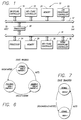
- Fig. 1 is a simplified block diagram of the dual bus local area network interfacing system 10 of the present invention.
- the system 10 includes a first internal bus 12 and a second internal bus 14.
- the first bus is a direct memory access (DMA) bus and the second bus 14 is a processor bus.
- DMA direct memory access
- a conventional backplane controller 16 first midplane controller 18, memory 20 and local area network frontplane controller 22' are attached to the DMA bus 12.
- a processor 24, memory 26, second midplane controller 30 and serial frontplane controller 32 are attached to the processor bus 14.
- communication between the DMA bus 12 and the processor bus 14 is provided by via a conventional transceiver 28 under control of the second midplane controller 30, the processor 24, memory 26 and serial frontplane controller may be of conventional design.
- the dual bus architecture of the LAN interfacing system of the present invention affords high speed operation with a simple and inexpensive architecture.
- the advantageous operation of the present invention derives from location of the bus intensive processor on a separate bus. This allows for processor operations to be executed without interference with LAN I/O operations. Communication between busses is facilitated through the transceiver 28 under the control of the second midplane controller 30, a bus arbiter as discussed more fully below.
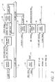
- Fig. 2 is a detailed block diagram of the dual bus local area network interfacing system 10 of the present invention.
- the backplane controller 16 is a conventional application specific integrated circuit (ASIC) that arbitrates between the DMA bus 12 and a backplane bus 17.
- the first midplane controller 18 arbitrates traffic on the DMA bus 12 in a conventional manner.
- the memory 20 includes read-only memory (ROM) 19 which stores I/O dependent identification code for the system 10, dynamic random access memory DRAM 21 which acts as a data buffer, and an electrically erasable programmable read-only memory (EEPROM) 23 which stores special parameters such as baud rate, password and etc.
- the frontplane controller 22 is a conventional LAN controller suitable for the IEEE 802.3 standard for example.
- the frontplane controller 22 is connected to the LAN by a serial interface adapter 44 (SIA), a transformer 46 and a transceiver 48 via a BNC port 49 an AUT port 47 to an external transceiver.
- SIA serial interface adapter 44
- the memory 26 is implemented with RON 29 which stores instructions for the processor 24, static random access memory (SRAM) 27, and EEPROM 29 for bug fixes, updates and etc.
- the serial frontplane controller 32 is implemented with an octart, an eight port universal asynchronous receiver-transmitter (UART) which communicates with a terminal or console through an RS-232 port 34.
- a context register 36 stores information relating to the status of the octart 32.
- Glue logic 40 provides signals for a display panel (not shown) relating to host processor activity, external controls, etc.
- Fig. 3 is a functional block diagram of an illustrative implementation of the second midplane controller 30 of the dual bus local area network interfacing system of the present invention.
- the second midplane controller 30 includes an address decoder 52, read/write control 54, a control/status register 56, an interrupt status register 58, across bus control logic 60, DTACK control 62 and reset control 64. With the exception of the across bus control logic 60, the functional elements of the second midplane controller 30 are of conventional design.
- the across bus control logic 60 is the central functional element of the second midplane controller 30.
- the across bus control logic 60 consists of two registered programmable logic array (PAL) circuits.
- the first PAL is denominated as Across Bus Controller Block and generates signals needed to allow the processor 24 to "go across” to the DMA bus 12.
- the Across Bus Controller Block includes two state machines “ND ACCESS” and “READ/WRITE”.
- Fig. 4 is a state diagram of the ND ACCESS state machine. Initially, the machine is in the idle state. In the illustrative implementation, when the highest bit of an address is a logical "1", a signal is provided that the processor 24 is attempting to access the DMA bus 12. By asserting the address strobe (NPAS) and processor address 23 (PADDR23), the processor 24 signals for across bus access. Thus, by monitoring the processor address strobe "NPAS" and the processor address line 23 "PADDR23" the state machine will know when to transition from the idle state to the ND ACCESS state. The outputs of the machine are shown within the circles. On transition from the idle state to the need access state, the NNDACC output goes from high to low to signal other state machines that this particular state machine has detected that the processor needs to access the DMA bus 12.
- NPAS address strobe
- PADDR23 processor address 23
- the ND ACCESS machine looks for NLAST, a signal from another state machine which determines if the current cycle is the last one of a current access cycle. On receipt of an NLAST signal, the machine provides a dump signal DUMP2 and resets the need access signal NNDACC and transitions to the ND DONE state. Thereafter, the ND ACCESS state machine automatically transitions back to the idle state.
- the state diagram of the read/write state machine of the first PAL of the Across Bus Control Logic of the second midplane controller is shown in Fig. 5. It controls the data transceivers and address latches between the DMA bus and the processor bus. The data bus goes from the processor side to the DMA side during a write access and vice versa during a read access. This state machine will keep controlling the DMA bus until NLAST is asserted.
- the second internal PAL of the across bus control logic 60 contains three state machines "WHOBUS”, “TRANSFER” and “LASTCYCLE".
- Figs. 6, 7, and 8 are state diagrams of the WHOBUS, TRANSFER and LASTCYCLE state machines respectively. Each state machine is clocked by a negative clock.
- a negative clock is a clock signal that triggers on the trailing edge thereof. The negative clock is used to minimize the across bus access time.
- the WHOBUS state machine determines which component has control of the DMA bus. (No component connected to the DMA bus may access the processor bus.) The WHOBUS state machine guarantees that the first midplane controller 18 will not attempt to use the DMA bus 12 when the processor 24 is transferring information across the DMA bus.
- the idle state is UPBUS for microprocessor bus. Ordinarily, the processor 24 has control of the DMA bus 12. When access to the bus is requested through the first midplane controller 18, the request is handled by the second midplane controller 30. This is illustrated in the state diagram of Fig. 6. In Fig. 6, the idle state is UPBUS for microprocessor owning the DMA bus.
- the TRANSFER state machine generates a signal (NGOX) which indicates that across bus transfers are permissible. This drives the READ/WRITE state machine and generates the signals to enable the address and data transceivers (NXDAT, NXDS, NXDATA, NXADDR).
- This state machine is designed to provide a single clock pulse signal for notifying the READ/WRITE state machine that it can start the across bus cycle.
- the LASTCYCLE state machine waits to see the DMA acknowledge data with a !NDDTAC. When this signal is true and the need access signal NNDACC signal is true, LASTCYCLE state machine transitions from the idle CLOSELAST state to the DELAST state.
- Fig. 9 is a timing diagram for an across bus read cycle of the dual bus local area network interfacing system of the present invention.
- Fig. 10 is a timing diagram for an across bus write cycle of the dual bus local area network interfacing system of the present invention.
- the processor asserts the address strobe NPAS and the data strobe NPDS when across bus read access is commanded.
- an across bus cycle may be detected by the ND-ACCESS state machine so the need access signal NNDACC is asserted.
- the NGOX signal goes low (active) and signals other state machines that across bus transfers are permissible on subsequent clock pulses as is indicated by the arrows on the diagram. That is, when data is transmitted across the bus, NXDAT is active which turns on the transceiver 28.
- NXADDR is a signal to place the address on the bus and etc. After these and other signals are presented, the slave devices should respond.
- a DMA DTAC signal (e.g., NDDTAC) is asserted which indicates that data is available on the bus for the processor.
- This signal passes through the transceiver 28 and becomes NPDTAC for the processor.
- the processor captures the data, removes the bus request and the NLAST signal is generated with detection of a DTACK signal on the DMA bus which frees the DMA bus.
- Write operations are depicted in the timing diagram of Fig. 10. Write operations are essentially the same as read operations with the exception that instead of waiting for data to come in on the data bus, data is placed on the data bus.
- the address decoder 52 decodes addresses in a conventional manner.
- the read/write controller 54 generates chip selects and provides read and write signals to the ROM and SRAM to provide control signals to memory.
- the DTACK controller is a state machine for notifying the processor when data are available from different devices with unique associated waits states.
- the remaining elements, i.e., control status register, interrupt status register and reset control are of conventional design and function.
Abstract
Description
- The present invention relates to local area networks (LANs). More specifically, the present invention relates to interfacing units for use with local area networks.
- While the present invention is described herein with reference to illustrative embodiments for particular applications, it should be understood that the invention is not limited thereto. Those having ordinary skill in the art and access to the teachings provided herein will recognize additional modifications, applications, and embodiments within the scope thereof and additional fields in which the present invention would be of significant utility.
- Local area networks (LANs) facilitate data communication between computing systems. Currently, several types of LAN systems are used widely in the art. Most systems may be classified generally as either an Ethernet, Token Ring, or 10 Base T type local area network.
- The Ethernet system is characterized by a coaxial cable which serves as a bus. The nodes of the system (e.g., terminals, printers and other devices) are connected to the cable and assigned a unique address.
- A Token Ring LAN is a circular network similar to the Ethernet system with the exception that a token is used to control access to the network. The token is a packet of signals that is passed from node to node. The node that has the token has control of the network with respect to the transmission of data to other nodes. When the node has completed a transmission, the token is released for acquisition by another node.
- The 10 Base T local area network is characterized by the use of a pair of twisted wires as a connector between nodes arranged in a star configuration around a controlling hub.
- With each system, an interface is required between the network and the host. The interface typically includes a frontplane for connection to the network and a backplane for connection to the host. Conventional local area network interfaces typically include a microprocessor and a single internal bus. The microprocessor typically ties up the internal bus for instruction fetch and execution operations. This precludes the use of the bus for input and output (I/O) operations thereby slowing the operation of the system.
- Some interfaces have been equipped with more powerful processors which tend to be less restrictive on I/O operations. However, these processors are expensive and typically require extensive, costly changes in the architecture of the interfacing system.
- Accordingly, there is a need in the art for a fast and inexpensive system for interfacing a local area network to host.
- The need in the art is addressed by the present invention which provides an improved local area network interfacing system. The inventive system includes a frontplane circuit for connecting the interfacing system to a local area network and a backplane circuit for connecting the interfacing system to a host. A first internal bus is included for providing communication between the backplane circuit and the frontplane circuit. A processor is included for controlling the operation of the interfacing system. A second internal bus is included for providing communication between the processor and associated memory. An internal bus control circuit facilitates and controls communication between the first internal bus and the second internal bus.
- The dual internal busses of the interfacing system of the present invention afford high speed operation with an inexpensive processor by allowing for input and output operations to be completed without being impeded by processor operations.
- Fig. 1 is a simplified block diagram of the dual bus local area network interfacing system of the present invention.
- Fig. 2 is a detailed block diagram of the dual bus local area network interfacing system of the present invention.
- Fig. 3 is a functional block diagram of an illustrative implementation of the second midplane controller of the dual bus local area network interfacing system of the present invention.
- Fig. 4 is a state diagram of the ND ACCESS state machine of the second midplane controller of the dual bus local area network interfacing system of the present invention.
- Fig. 5 is a state diagram of the read/write state machine of the Across Bus Control Logic of the second midplane controller of the dual bus local area network interfacing system of the present invention.
- Fig. 6 is a state diagram of the WHOBUS state machine of the Across Bus Control Logic of the second midplane controller of the dual bus local area network interfacing system of the present invention.
- Fig. 7 is a state diagram of the TRANSFER state machine of the Across Bus Control Logic of the second midplane controller of the dual bus local area network interfacing system of the present invention.
- Fig. 8 is a state diagram of the LASTCYCLE state machine of the Across Bus Control Logic of the second midplane controller of the dual bus local area network interfacing system of the present invention.
- Fig. 9 is a timing diagram for an across bus read cycle of the dual bus local area network interfacing system of the present invention.
- Fig. 10 is a timing diagram for an across bus write cycle of the dual bus local area network interfacing system of the present invention.
- Illustrative embodiments and exemplary applications will now be described with reference to the accompanying drawings to disclose the advantageous teachings of the present invention.
- Fig. 1 is a simplified block diagram of the dual bus local area
network interfacing system 10 of the present invention. Thesystem 10 includes a firstinternal bus 12 and a secondinternal bus 14. In the illustrative embodiment, the first bus is a direct memory access (DMA) bus and thesecond bus 14 is a processor bus. - A
conventional backplane controller 16,first midplane controller 18,memory 20 and local area network frontplane controller 22' are attached to theDMA bus 12. Aprocessor 24,memory 26,second midplane controller 30 andserial frontplane controller 32 are attached to theprocessor bus 14. As discussed more fully below, communication between theDMA bus 12 and theprocessor bus 14 is provided by via aconventional transceiver 28 under control of thesecond midplane controller 30, theprocessor 24,memory 26 and serial frontplane controller may be of conventional design. - As discussed more fully below, the dual bus architecture of the LAN interfacing system of the present invention affords high speed operation with a simple and inexpensive architecture. The advantageous operation of the present invention derives from location of the bus intensive processor on a separate bus. This allows for processor operations to be executed without interference with LAN I/O operations. Communication between busses is facilitated through the
transceiver 28 under the control of thesecond midplane controller 30, a bus arbiter as discussed more fully below. - Fig. 2 is a detailed block diagram of the dual bus local area
network interfacing system 10 of the present invention. Thebackplane controller 16 is a conventional application specific integrated circuit (ASIC) that arbitrates between theDMA bus 12 and abackplane bus 17. Thefirst midplane controller 18 arbitrates traffic on theDMA bus 12 in a conventional manner. Thememory 20 includes read-only memory (ROM) 19 which stores I/O dependent identification code for thesystem 10, dynamic randomaccess memory DRAM 21 which acts as a data buffer, and an electrically erasable programmable read-only memory (EEPROM) 23 which stores special parameters such as baud rate, password and etc. Thefrontplane controller 22 is a conventional LAN controller suitable for the IEEE 802.3 standard for example. Thefrontplane controller 22 is connected to the LAN by a serial interface adapter 44 (SIA), atransformer 46 and atransceiver 48 via aBNC port 49 anAUT port 47 to an external transceiver. - On the
processor bus 14, thememory 26 is implemented with RON 29 which stores instructions for theprocessor 24, static random access memory (SRAM) 27, and EEPROM 29 for bug fixes, updates and etc. Theserial frontplane controller 32 is implemented with an octart, an eight port universal asynchronous receiver-transmitter (UART) which communicates with a terminal or console through an RS-232port 34. Acontext register 36 stores information relating to the status of theoctart 32.Glue logic 40 provides signals for a display panel (not shown) relating to host processor activity, external controls, etc. - As mentioned above, communication between the internal I/O
DMA communication bus 12 and theinternal processor bus 14 is arbitrated by thesecond midplane controller 30 via thetransceiver 28. - Fig. 3 is a functional block diagram of an illustrative implementation of the
second midplane controller 30 of the dual bus local area network interfacing system of the present invention. Thesecond midplane controller 30 includes anaddress decoder 52, read/writecontrol 54, a control/status register 56, an interruptstatus register 58, acrossbus control logic 60,DTACK control 62 and resetcontrol 64. With the exception of the acrossbus control logic 60, the functional elements of thesecond midplane controller 30 are of conventional design. - The across
bus control logic 60 is the central functional element of thesecond midplane controller 30. In the illustrative embodiment, the acrossbus control logic 60 consists of two registered programmable logic array (PAL) circuits. - The first PAL is denominated as Across Bus Controller Block and generates signals needed to allow the
processor 24 to "go across" to theDMA bus 12. The Across Bus Controller Block includes two state machines "ND ACCESS" and "READ/WRITE". - Fig. 4 is a state diagram of the ND ACCESS state machine. Initially, the machine is in the idle state. In the illustrative implementation, when the highest bit of an address is a logical "1", a signal is provided that the
processor 24 is attempting to access theDMA bus 12. By asserting the address strobe (NPAS) and processor address 23 (PADDR23), theprocessor 24 signals for across bus access. Thus, by monitoring the processor address strobe "NPAS" and theprocessor address line 23 "PADDR23" the state machine will know when to transition from the idle state to the ND ACCESS state. The outputs of the machine are shown within the circles. On transition from the idle state to the need access state, the NNDACC output goes from high to low to signal other state machines that this particular state machine has detected that the processor needs to access theDMA bus 12. - In the ND ACCESS state, the ND ACCESS machine looks for NLAST, a signal from another state machine which determines if the current cycle is the last one of a current access cycle. On receipt of an NLAST signal, the machine provides a dump signal DUMP2 and resets the need access signal NNDACC and transitions to the ND DONE state. Thereafter, the ND ACCESS state machine automatically transitions back to the idle state.
- The state diagram of the read/write state machine of the first PAL of the Across Bus Control Logic of the second midplane controller is shown in Fig. 5. It controls the data transceivers and address latches between the DMA bus and the processor bus. The data bus goes from the processor side to the DMA side during a write access and vice versa during a read access. This state machine will keep controlling the DMA bus until NLAST is asserted.
- The second internal PAL of the across
bus control logic 60 contains three state machines "WHOBUS", "TRANSFER" and "LASTCYCLE". Figs. 6, 7, and 8 are state diagrams of the WHOBUS, TRANSFER and LASTCYCLE state machines respectively. Each state machine is clocked by a negative clock. A negative clock is a clock signal that triggers on the trailing edge thereof. The negative clock is used to minimize the across bus access time. - The WHOBUS state machine determines which component has control of the DMA bus. (No component connected to the DMA bus may access the processor bus.) The WHOBUS state machine guarantees that the
first midplane controller 18 will not attempt to use theDMA bus 12 when theprocessor 24 is transferring information across the DMA bus. In Fig. 6, the idle state is UPBUS for microprocessor bus. Ordinarily, theprocessor 24 has control of theDMA bus 12. When access to the bus is requested through thefirst midplane controller 18, the request is handled by thesecond midplane controller 30. This is illustrated in the state diagram of Fig. 6. In Fig. 6, the idle state is UPBUS for microprocessor owning the DMA bus. When the first midplane controller bus request signal NFBR is active and an active no data transmission signal !NXDAT is high (as indicated by an exclamation mark "!") no across bus access is taking place, the bus is placed under the control of thefirst midplane controller 18 and the machine transitions to the FULBUS state. The NFBG (bus granted) signal is set high and DUMPOUT signal is set high permitting data transfers on the DMA bus. When the first midplane controller removes the bus request, NFBR and DUMPOUT are reset and the machine transitions to the ENDBUS state and theprocessor 24 is allowed to reacquire theDMA bus 12. As illustrated in Fig.7, the TRANSFER state machine generates a signal (NGOX) which indicates that across bus transfers are permissible. This drives the READ/WRITE state machine and generates the signals to enable the address and data transceivers (NXDAT, NXDS, NXDATA, NXADDR). This state machine is designed to provide a single clock pulse signal for notifying the READ/WRITE state machine that it can start the across bus cycle. Next, as illustrated in Fig. 8, the LASTCYCLE state machine waits to see the DMA acknowledge data with a !NDDTAC. When this signal is true and the need access signal NNDACC signal is true, LASTCYCLE state machine transitions from the idle CLOSELAST state to the DELAST state. Once NDDTAC is generated, the signal NLAST is generated on the falling edge. NLAST drives the ND ACCESS state machine to de-assert NNDACC on the next rising edge clock pulse. The operation of the present invention is appreciated with the state diagrams in conjunction with Figs. 9 and 10. Fig. 9 is a timing diagram for an across bus read cycle of the dual bus local area network interfacing system of the present invention. Fig. 10 is a timing diagram for an across bus write cycle of the dual bus local area network interfacing system of the present invention. - In Fig. 9, the processor asserts the address strobe NPAS and the data strobe NPDS when across bus read access is commanded. By decoding the address lines and detecting a logical "1" at the highest address bit, an across bus cycle may be detected by the ND-ACCESS state machine so the need access signal NNDACC is asserted. Half a clock pulse later, the NGOX signal goes low (active) and signals other state machines that across bus transfers are permissible on subsequent clock pulses as is indicated by the arrows on the diagram. That is, when data is transmitted across the bus, NXDAT is active which turns on the
transceiver 28. NXADDR is a signal to place the address on the bus and etc. After these and other signals are presented, the slave devices should respond. A short time later, a DMA DTAC signal (e.g., NDDTAC) is asserted which indicates that data is available on the bus for the processor. This signal passes through thetransceiver 28 and becomes NPDTAC for the processor. The processor captures the data, removes the bus request and the NLAST signal is generated with detection of a DTACK signal on the DMA bus which frees the DMA bus. These activities are represented by the topmost state of the READ/WRITE state diagram of Fig. 5. - Write operations are depicted in the timing diagram of Fig. 10. Write operations are essentially the same as read operations with the exception that instead of waiting for data to come in on the data bus, data is placed on the data bus.
- Returning to Fig. 3, the
address decoder 52 decodes addresses in a conventional manner. The read/write controller 54 generates chip selects and provides read and write signals to the ROM and SRAM to provide control signals to memory. The DTACK controller is a state machine for notifying the processor when data are available from different devices with unique associated waits states. The remaining elements, i.e., control status register, interrupt status register and reset control are of conventional design and function. - Thus, the present invention has been described herein with reference to a particular embodiment for a particular application. Those having ordinary skill in the art and access to the present teachings will recognize additional modifications applications and embodiments within the scope thereof.
- It is therefore intended by the appended claims to cover any and all such applications, modifications and embodiments within the scope of the present invention.
- Accordingly,
Claims (8)
- A local area network interfacing system comprising:
frontplane means for connecting said interfacing system to a local area network;
backplane means for connecting said interfacing system to a host;
a first internal bus for providing communication between said backplane means and said frontplane means;
processor means for controlling the operation of said interfacing system;
a second internal bus for providing communication between said processor means and associated memory; and
internal bus control means for facilitating and controlling communication between said first internal bus and said second internal bus. - The invention of Claim 1 wherein said internal bus control means includes interbus communication logic means for controlling communication between said first internal bus and second internal bus.
- The invention of Claims 1 or 2 wherein said internal bus control means includes a data transceiver connected between said first internal bus and said second internal bus.
- The invention of any one of the preceding claims including a local area network controller connected to said first internal bus.
- The invention of any one of the preceding claims including a backplane controller connected to said first internal bus.
- The invention of any one of the preceding claims including a direct memory access control means for controlling communication on said first internal bus.
- A local area network interfacing system comprising:
frontplane means for connecting said interfacing system to a local area network;
backplane means for connecting said interfacing system to a host;
a first internal bus for providing communication between said backplane means and said frontplane means;
a local area network controller connected to said first internal bus;
a backplane controller connected to said first internal bus;
direct memory access control means for controlling communication on said first internal bus;
a processor for controlling the operation of said interfacing system;
a second internal bus for providing communication between said processor and associated memory; and
internal bus control means for facilitating and controlling communication between said first internal bus and said second internal bus, said internal bus control means including a data transceiver connected between said first internal bus and said second internal bus and interbus communication logic means for controlling communication between said first internal bus and said second internal bus via said data transceiver. - A local area network interfacing method including the steps of:a) connecting an interfacing system to a local area network;b) connecting said interfacing system to a host;c) providing communication between a backplane and a frontplane via a first internal bus;d) controlling the operation of said interfacing system with a processor;e) providing communication between said processor and associated memory with a second internal bus; andf) facilitating and controlling communication between said first internal bus and said second internal bus.
Applications Claiming Priority (2)
| Application Number | Priority Date | Filing Date | Title |
|---|---|---|---|
| US907955 | 1992-07-02 | ||
| US07/907,955 US5355452A (en) | 1992-07-02 | 1992-07-02 | Dual bus local area network interfacing system |
Publications (2)
| Publication Number | Publication Date |
|---|---|
| EP0577110A2 true EP0577110A2 (en) | 1994-01-05 |
| EP0577110A3 EP0577110A3 (en) | 1995-04-19 |
Family
ID=25424923
Family Applications (1)
| Application Number | Title | Priority Date | Filing Date |
|---|---|---|---|
| EP93110469A Withdrawn EP0577110A3 (en) | 1992-07-02 | 1993-06-30 | Dual bus local area metwork interfacing system. |
Country Status (3)
| Country | Link |
|---|---|
| US (1) | US5355452A (en) |
| EP (1) | EP0577110A3 (en) |
| JP (1) | JPH0697938A (en) |
Families Citing this family (8)
| Publication number | Priority date | Publication date | Assignee | Title |
|---|---|---|---|---|
| ATE195823T1 (en) * | 1993-07-08 | 2000-09-15 | Koninkl Kpn Nv | COMPUTER SYSTEM THAT HAS A PROCESSOR AND A MEMORY AREA THAT INCLUDES A COMPUTER INTERFACE |
| US5805927A (en) * | 1994-01-28 | 1998-09-08 | Apple Computer, Inc. | Direct memory access channel architecture and method for reception of network information |
| US5655151A (en) * | 1994-01-28 | 1997-08-05 | Apple Computer, Inc. | DMA controller having a plurality of DMA channels each having multiple register sets storing different information controlling respective data transfer |
| US5828856A (en) * | 1994-01-28 | 1998-10-27 | Apple Computer, Inc. | Dual bus concurrent multi-channel direct memory access controller and method |
| US5519641A (en) * | 1994-05-20 | 1996-05-21 | International Business Machines Corporation | Method and apparatus for configuring plural multimedia audio cards as a local area network |
| US5684956A (en) * | 1994-11-14 | 1997-11-04 | Billings; Roger E. | Data transmission system with parallel packet delivery |
| US5664152A (en) * | 1995-06-06 | 1997-09-02 | Hewlett-Packard Company | Multiple segmenting of main memory to streamline data paths in a computing system |
| US6760339B1 (en) * | 2000-05-20 | 2004-07-06 | Equipe Communications Corporation | Multi-layer network device in one telecommunications rack |
Citations (2)
| Publication number | Priority date | Publication date | Assignee | Title |
|---|---|---|---|---|
| US4771286A (en) * | 1986-07-28 | 1988-09-13 | Honeywell Bull Inc. | Lan controller having split bus design |
| US4908823A (en) * | 1988-01-29 | 1990-03-13 | Hewlett-Packard Company | Hybrid communications link adapter incorporating input/output and data communications technology |
Family Cites Families (11)
| Publication number | Priority date | Publication date | Assignee | Title |
|---|---|---|---|---|
| US4313162A (en) * | 1979-12-14 | 1982-01-26 | Burroughs Corporation | I/O Subsystem using data link processors |
| US4787082A (en) * | 1986-07-24 | 1988-11-22 | American Telephone And Telegraph Company, At&T Bell Laboratories | Data flow control arrangement for local area network |
| US4750114A (en) * | 1986-07-28 | 1988-06-07 | Honeywell Bull Inc. | Local area network control block |
| US4715030A (en) * | 1986-08-04 | 1987-12-22 | General Electric Company | Local area network bridge |
| US4672570A (en) * | 1986-09-05 | 1987-06-09 | The United States Of America As Represented By The Secretary Of The Air Force | Network interface module and method |
| US5001707A (en) * | 1989-11-02 | 1991-03-19 | Northern Telecom Limited | Method of providing reserved bandwidth in a dual bus system |
| US5226120A (en) * | 1990-05-21 | 1993-07-06 | Synoptics Communications, Inc. | Apparatus and method of monitoring the status of a local area network |
| US5206936A (en) * | 1990-08-31 | 1993-04-27 | International Business Machines Corporation | Apparatus for exchanging channel adapter status among multiple channel adapters |
| US5103446A (en) * | 1990-11-09 | 1992-04-07 | Moses Computers, Inc. | Local area network adaptive throughput control for instantaneously matching data transfer rates between personal computer nodes |
| US5235597A (en) * | 1991-03-08 | 1993-08-10 | International Business Machines Corp. | Synchronizing asynchronous protocol interactions between peer layers in different nodes of a layered communication network |
| US5239632A (en) * | 1992-04-16 | 1993-08-24 | Hewlett-Packard Company | Device to translate logical unit number communications on one SCSI bus to ID communications on a subordinate SCSI bus |
-
1992
- 1992-07-02 US US07/907,955 patent/US5355452A/en not_active Expired - Lifetime
-
1993
- 1993-06-30 EP EP93110469A patent/EP0577110A3/en not_active Withdrawn
- 1993-07-02 JP JP5190802A patent/JPH0697938A/en active Pending
Patent Citations (2)
| Publication number | Priority date | Publication date | Assignee | Title |
|---|---|---|---|---|
| US4771286A (en) * | 1986-07-28 | 1988-09-13 | Honeywell Bull Inc. | Lan controller having split bus design |
| US4908823A (en) * | 1988-01-29 | 1990-03-13 | Hewlett-Packard Company | Hybrid communications link adapter incorporating input/output and data communications technology |
Also Published As
| Publication number | Publication date |
|---|---|
| US5355452A (en) | 1994-10-11 |
| JPH0697938A (en) | 1994-04-08 |
| EP0577110A3 (en) | 1995-04-19 |
Similar Documents
| Publication | Publication Date | Title |
|---|---|---|
| JP3604398B2 (en) | High-speed parallel packetized module arbitration control and data bus | |
| US5321819A (en) | Interface for coupling a host device having a network interface to a computer network having a predetermined communications medium and a predetermined communications physical layer | |
| US6014729A (en) | Shared memory arbitration apparatus and method | |
| US5299193A (en) | Signal interface for coupling a network front end circuit to a network adapter circuit | |
| US4381542A (en) | System for interrupt arbitration | |
| KR100295968B1 (en) | Burst-broadcasting on a peripheral component interconnect bus | |
| EP0458304B1 (en) | Direct memory access transfer controller and use | |
| US6134625A (en) | Method and apparatus for providing arbitration between multiple data streams | |
| GB2264845A (en) | Local area network adaptive circuit for multiple network types | |
| JPH0690699B2 (en) | Interrupt interface circuit | |
| JPH03160545A (en) | Interface circuit | |
| JPH08255124A (en) | System and method for data processing | |
| EP0465221B1 (en) | IEEE 488 Interface | |
| US5355452A (en) | Dual bus local area network interfacing system | |
| US5748918A (en) | Method and apparatus for supporting two subtractive decode agents on the same bus in a computer system | |
| JPS58502027A (en) | Peripherals adapted to monitor low data rate serial input/output interfaces | |
| JPS6237428B2 (en) | ||
| US6012117A (en) | Methods and apparatus for arbitrating and controlling arbitration for access to a serial bus | |
| US5812878A (en) | System for DMA transfer wherein controller waits before execution of next instruction until a counter counts down from a value loaded by said controller | |
| JP2860733B2 (en) | Bus connection device | |
| EP0567342A2 (en) | Signal interface for coupling a network front end circuit to a network adapter circuit | |
| JPH10303948A (en) | Communication device and its method | |
| JPH07244633A (en) | Interface device | |
| JPH01108665A (en) | Dma transfer control system | |
| JPH05210623A (en) | Microprocessor and data processor |
Legal Events
| Date | Code | Title | Description |
|---|---|---|---|
| PUAI | Public reference made under article 153(3) epc to a published international application that has entered the european phase |
Free format text: ORIGINAL CODE: 0009012 |
|
| AK | Designated contracting states |
Kind code of ref document: A2 Designated state(s): DE FR GB |
|
| PUAL | Search report despatched |
Free format text: ORIGINAL CODE: 0009013 |
|
| AK | Designated contracting states |
Kind code of ref document: A3 Designated state(s): DE FR GB |
|
| 17P | Request for examination filed |
Effective date: 19951009 |
|
| RAP1 | Party data changed (applicant data changed or rights of an application transferred) |
Owner name: HEWLETT-PACKARD COMPANY, A DELAWARE CORPORATION |
|
| STAA | Information on the status of an ep patent application or granted ep patent |
Free format text: STATUS: THE APPLICATION IS DEEMED TO BE WITHDRAWN |
|
| 18D | Application deemed to be withdrawn |
Effective date: 20010103 |