EP0577883A1 - Convertisseur analogique-numérique - Google Patents
Convertisseur analogique-numérique Download PDFInfo
- Publication number
- EP0577883A1 EP0577883A1 EP92201595A EP92201595A EP0577883A1 EP 0577883 A1 EP0577883 A1 EP 0577883A1 EP 92201595 A EP92201595 A EP 92201595A EP 92201595 A EP92201595 A EP 92201595A EP 0577883 A1 EP0577883 A1 EP 0577883A1
- Authority
- EP
- European Patent Office
- Prior art keywords
- stage
- analog
- voltage
- digital converter
- stages
- Prior art date
- Legal status (The legal status is an assumption and is not a legal conclusion. Google has not performed a legal analysis and makes no representation as to the accuracy of the status listed.)
- Granted
Links
Images

Classifications
-
- H—ELECTRICITY
- H03—ELECTRONIC CIRCUITRY
- H03M—CODING; DECODING; CODE CONVERSION IN GENERAL
- H03M1/00—Analogue/digital conversion; Digital/analogue conversion
- H03M1/12—Analogue/digital converters
- H03M1/14—Conversion in steps with each step involving the same or a different conversion means and delivering more than one bit
- H03M1/144—Conversion in steps with each step involving the same or a different conversion means and delivering more than one bit the steps being performed sequentially in a single stage, i.e. recirculation type
-
- H—ELECTRICITY
- H03—ELECTRONIC CIRCUITRY
- H03M—CODING; DECODING; CODE CONVERSION IN GENERAL
- H03M1/00—Analogue/digital conversion; Digital/analogue conversion
- H03M1/12—Analogue/digital converters
- H03M1/14—Conversion in steps with each step involving the same or a different conversion means and delivering more than one bit
- H03M1/145—Conversion in steps with each step involving the same or a different conversion means and delivering more than one bit the steps being performed sequentially in series-connected stages
- H03M1/146—Conversion in steps with each step involving the same or a different conversion means and delivering more than one bit the steps being performed sequentially in series-connected stages all stages being simultaneous converters
- H03M1/147—Conversion in steps with each step involving the same or a different conversion means and delivering more than one bit the steps being performed sequentially in series-connected stages all stages being simultaneous converters at least two of which share a common reference generator
Definitions
- the present invention relates to an analog to digital converter for converting an analog input voltage to a digital output voltage, and which includes at least two cascaded first and second switching means controlled voltage divider stages each of which includes a plurality of series connected substages, an input control voltage applied to a said stage being subdivided therein so as to produce subdivided voltages, said input voltage of said first stage being constituted by a predetermined reference voltage, and said subdivided voltages of said stages being successively compared with said analog voltage in a logic means also included in said analog to digital converter thereby generating subsequent parts of said digital output voltage.
- Such an analog to digital converter is known in the art, and is e.g. described in "Session 1 : Data converters - WAM 1.2 : a CMOS 40 MHz 8b 105 mW Two-Step ADC" of the Proceedings of ISCC 89, February 15, 1989, pp. 14-18.
- the two stages are interlaced in such a way that they form a single network of 256 resistors of equal value.
- the subdivided voltages of the first or coarse stage are taken from the resistor network every sixteenth resistor. This gives 15 voltages which are derived from a reference voltage and compared with the analog voltage by coarse comparators. The result thereof indicates the level of the analog voltage and determines which switches of the switching means are to be closed as well as which sixteen cascaded resistors are used as resistors of the second or fine stage to supply the subdivided voltages of this fine stage.
- a disadvantage of this known converter is that the switches connecting the resistors to the comparators of the fine stage are operated at a voltage depending on the level of the analog input voltage since the choice of which cascaded resistors constitute the fine stage is dependent upon the analog input voltage. As a consequence and because the switches have a series resistance depending on the voltage they are operated at, the resistance introduced in the fine stage by the switches depends on the analog voltage, and thereby introduces linearity errors.
- An object of the invention is to provide a converter of the above type but which does not have the above mentioned drawback.
- the input voltage of said one stage is determined when the part of the switching means connecting this one stage to the prior stage is to be set.
- the resistance introduced by that part of the switching means becomes independent of the setting of the latter part, unlike the prior art where the input voltage of a stage, being the voltage applied to the part of the switching means connecting that stage to the prior stage depends on the setting of the latter part and, hence, also the series resistance introduced depends on the setting of the latter part.
- the linearity errors become lower with respect to the prior art.
- Another characteristic of the invention is that for each one of said stages, the first one excepted, said input control voltage is constituted by an output control voltage produced over a substage of the stage preceding said one stage.
- each next stage subdivides the reference voltage further with respect to the prior stage.
- a further characteristic of the invention is that for each two consecutive stages, the second stage thereof constitutes the substage of the first stage over which said output control voltage of said first stage is produced.
- Still another characteristic of the invention is that said one stage is said first stage.
- the reference voltage is applied to the first stage via the switching means, which means that the voltage applied to the part of the switching means included in the first stage is fixed and known and, hence, the voltage drop over the switching means is independent of the analog voltage.
- linearity errors are no longer present. It is to be noted that a gain error and an offset error are still present. However, such errors do not affect the linearity of the converter.
- each of said stages includes a logic part, which is part of said logic means, and an output of which is one of said subsequent parts of said digital output voltage, in that each but said first stage includes a switching part, which is part of said switching means, and in that, for each but said last stage, said output of said logic part controls said switching part of each next stage.
- each stage is an autonomous item, i.e. the stages only interchange control signals and, e.g., no analog voltages.
- the stages being less dependent upon each other, the design of the converter becomes easier.
- a further feature of the invention is that for each of said stages, said logic part is controlled by the voltages at junction points of those substages corresponding to said output substage of the prior stage, the latter substages for said first stage being constituted by all of the substages thereof.
- Each next stage so generates voltage levels, a voltage level being the voltage region in between two subdivided voltages or the reference voltage or the ground, and which constitute finer voltage regions than the voltage levels of the output substage of the prior stage. Thereby a better resolution is obtained in each subsequent stage.
- Still a further feature of the invention is that said analog input voltage is, for each considered stage, so delayed that said outputs of the respective logic parts of the respective prior stages are available when said analog input voltage is applied to said considered stage.
- each of said subsequent parts of said digital signal forthcoming from said respective stages is constituted by a predetermined number of bits.
- Each stage indeed provides a number of voltage levels, which corresponds to a predetermined number of bits.
- the number of levels provided is a power of two and as a result the conversion of the levels to bits can be done per stage instead of integrated with other stages, which again allows an easier design.
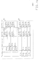
- the analog to digital converter ADC1 shown in Fig. 1a and b is adapted to convert the amplitude of an analog input voltage Vin to a 6 bit digital output voltage or digital signal Dout. It includes three switching means controlled resistive voltage divider stages B1, B2 and B3 each including a number of substages, each constituted by a resistor. Stage B3 includes four series connected resistors R31 to R34 each having the same value r and constitutes a substage of stage B2. Indeed, B3 is connected in series between two networks of three cascaded resistors R21a to R23a and R21b to R23b forming part of B2 and all having the same value 4r.
- stage B2 constitutes a substage of stage B1 and is connected in the same way as stage B3 in series between two networks of three cascaded resistors each, R11a to R13a and R11b to R13b, which all have the same value 16r and form part of B1.
- Stages B1 and B2 furthermore include switching means, constituted by switches S11a to S14a and S11b to S14b, and S21a to S24a and S21b to S24b respectively, each switch being coupled between one of two inputs of the respective stages and the junction points of the resistors thereof, as shown in Fig. 1.
- the switching means of stage B1 furthermore includes a so-called double pole double throw switch S0 via which a reference voltage 0, Vref can be applied to the input of stage B1, either normally or reversely poled. All the above switches are in fact constituted by MOSFETs, which are neither shown nor described in detail since they are well known in the art.
- Each stage furthermore includes comparators comparing the above analog input voltage Vin which is to be converted to the digital signal Dout, to voltages occurring at the junction points of the resistors of the different stages.
- Stage B1 includes comparators C10a to C13a and C10b to C13b; stage B2 includes comparators C21a to C23a and C21b to C23b; and stage B3 includes comparators C31 to C33, all comparators being connected as shown in Fig. 1.
- the outputs of the comparators of each stage are applied to a string of logic EXOR gates also included in each stage and which translate the comparator outputs into a four level output, as will be explained later.
- the outputs of the comparators of stage B1 are applied to EXORs E10a to E13a and E10b to E13b, those of stage B2 to EXORs E20a to E23a and E20b to E23b, and those of stage B3 to EXOR's E30 to E33. All the EXORs are connected as shown in Fig. 1. Again part of the EXORs of stages B1 and B2 are superfluous as will be explained later. It is also noted that EXOR inputs which on Fig. 1 are connected to outputs of comparators which are not provided since they are superfluous or since underflow or overflow control is not a wanted feature, are then connected to a fixed voltage as will be explained later.
- the outputs of the EXORs of each stage are applied to not shown buffers, the outputs of the buffers of B1 and B2 controlling the switches of the same stage.
- the outputs of the buffers are furthermore applied to an encoder ENC, including the cascade connection of a delay circuit DEL and a digital-to-digital converter circuit BIT.
- the outputs of the buffers of stage B1 are delayed over two periods, whilst those of B2 are delayed over one period, the delay period corresponding with the delay between applying a voltage to the input of a stage and obtaining the corresponding buffer outputs for controlling the switches of the next stage.
- the delayed and not delayed buffer outputs are then converted by the digital-to-digital converter BIT, which is e.g. a triple four level to two bit decoder, so obtaining the digital signal Dout.
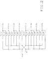
- Fig. 2 shows an alternative embodiment of the switching means included in stage B1 and shown in Fig. 1a and b.
- This embodiment includes MOSFET switches S11a' to S14a', S11a'' to S14a'', S11b' to S14b', S11b'' to S14b'' which are each coupled between one of the two inputs of stage B1 and the junction points of the resistors thereof as shown in Fig. 2 .
- the reference voltage 0, Vref can be applied to the resistor network with normal or reversed polarity but via only two switches in series, e.g. S11a' and S11b' or S11a'' and S11b'' for reversed polarity, instead of four in the case of Fig. 1 (e.g. S11a, S11b and two switches of S0).
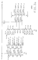
- the analog to digital converter ADC2 of Fig. 3 also includes three stages, B1', B2' and B3', each stage here operating as an independent analog to digital converter and being controlled by the output of all prior stages.
- Stage B1' is a two bit so-called flash analog to digital converter known in the art and built from cascaded resistors R1 to R4 over which the reference voltage 0, Vref is applied, the voltage at each junction point being compared with the analog input voltage Vin by comparators C0 to C4 respectively.
- the outputs of the comparators C0 to C4 are connected to the inputs of EXORs E0 to E3 respectively.
- comparators C0 and C4 merely serve to indicate overflow and underflow of the analog voltage Vin with respect to the reference voltage Vref respectively, and may be omitted.
- the EXOR inputs now connected to output of comparator C0 should then be connected to Vsat(+), which is the positive saturation voltage of the comparators, whereas the EXOR input now connected to the output of comparator C4 should then be connected to Vsat(-) which is the negative saturation voltage of the comparators.
- Stage B2' is a two stage analog to digital converter of the type shown in Fig. 1 but wherein the comparators of the first stage have been omitted. It is built up from switches S11c to S14c and S11d to S14d, resistors R11c to R13c, R11d to R13d and R21c to R24c, comparators C21c to C23c, and EXORs E20c to E23c respectively.
- the switches of stage B2' are controlled by the outputs of EXORs E0 to E3 of stage B1'.
- the analog voltage Vin is applied to the comparators via a a well known sample and hold circuit SH1, which compensates for the delay produced between the instants of applying Vin to stage B1' and operating the switches of stage B2'.
- Stage B3' is a three stage analog to digital converter of the type shown in Fig. 1 but wherein the comparators of first and second stage have been omitted. It is built up from switches S11f to S14f, S11g to S14g, S21f to S24f and S21g to S24g, resistors R11f to R13f, R11g to R13g, R21f to R23f, R21g to R23g and R31f to R34f, comparators C31f to C33f, and EXORs E30f to E33f.
- the switches S11f to S14f and S11g to S14g are controlled by the outputs of EXORs E0 to E3 of stage B1' via a sample and hold circuit SH3, and S21f to S24f and S21g to S24g by the outputs of EXORs E20c to E23c of stage B2'.
- SH3 provides a delay so that all switches of stage B3' are operated simultaneously.
- the analog voltage Vin is applied to the comparators via a sample and hold circuit SH2 which compensates for the delay between applying Vin to stage B1' and operating the switches of stage B3'.
- the outputs of the EXOR's are all applied to a not shown encoder which is similar to the encoder ENC of Fig. 1 and which encodes the EXOR outputs to a 6-bit digital signal Dout.
- the analog to digital converter ADC1 of Fig. 1 operates as follows.
- the analog voltage Vin applied to the positive inputs of the comparators is to be converted to the digital signal Dout, first all switches are opened, except for switches S11a, S11b, S21a and S21b.
- Switch S0 is set to its normal position so that the voltage applied to switch S11a is positive with respect to that applied to switch S11b.
- the reference voltage Vref is applied to series connected resistors R11a to R13a, R21a to R23a and R31 to R34.
- the voltages derived from Vref and occurring at the junction points of the resistors are then compared with the analog voltage Vin in the comparators C10a to C13a, C21a to C23a, C31 to C33 and C11b.
- Vin is higher than the voltage derived from Vref occurring at the negative input of the comparator, then the comparator output is at Vsat(+) which is the positive saturation voltage of the comparator.
- Vin is lower than the derived voltage mentioned, the comparator output is at Vsat(-) which is the negative saturation voltage of the comparator.
- the respective comparator outputs show a pattern of a number of successive Vsat (+) followed by a number of successive Vsat(-).
- each EXOR string these saturation voltages are then converted to a logical four level signal, each level being indicated by one of the EXORs and each but one of these levels being 0.
- the level which is on one indicates the transition from Vsat(+) to Vsat(-) of the corresponding comparators and hence the voltage range in which Vin is located.
- the output of EXOR E11a is a logical one
- the transition from Vsat(+) to Vsat (-) occurs from comparator C12a to comparator C11a. This means that Vin is lower than the voltage at the junction of resistors R11a and R12a, but higher than that at the junction of R12a and R13a.
- the underflow case can be solved by reversing the polarity of Vref by changing the position of switch S0.
- the EXORs E10a to E13a then still have an all 0 output, the absolute value of Vin is higher than Vref and can not be converted to a digital value unless as to an all 1 digital output.
- the difference between the first and the second above mentioned case can be made by monitoring the output of one of the comparators C10a to C13a and C11b.
- switches chosen above can be closed in a first step, i.e. S11a, S11b, S21a and S21b.
- four other switches can be chosen.
- the only imperative here is that for each stage two corresponding switches are closed, i.e. an a-switch and a b-switch of the same numerical index, e.g. S13a and S13b.
- other comparators and other EXORs become active, in the example comparators C12a, C13a, C11b to C13b and EXORs E12a, E13a , E11b and E12b, comparator C12a indicating overflow and C13b indicating underflow.
- comparators not used in the first step i.e. C12b, C13b and C10b in the former example (S21a and S11b closed), or C10a, C11a and C10b in the latter example (S13a and S13b closed), are superfluous, and can therefore be omitted.
- stage B1 whose output is a logical one indicates which switches of stage B1 are to be closed in order that the analog voltage Vin should fall within the voltage range applied over the resistors of stage B2. For instance, when the output of E10a is a logical one switches S11a and S11b are opened whereas switches S14a and S14b are closed.
- the original output signals of the EXORs of each stage are applied to the encoder ENC, the latter outputs being the ones before the switch settings of the stage itself, but after those of the prior stages were changed, i.e. according to the above example, the outputs of EXOR's E10a to E13a with switches S11a and S11b closed, the outputs of EXORs E20a to E23a with switches S14a and S14b, and S21a and S21b closed, and the outputs of EXORs E30 to E33 with switches S14a, S14b, S22a and S22b closed.
- the EXOR output signals of stages B1 and B2 are delayed over such a time value that the the EXOR outputs are simultaneously applied to the converter BIT included in encoder ENC.
- the digital-to-digital converter BIT converts the three four level signals from the EXORs to a 6 bit digital output signal Dout.
- the position of switch S0 is indicative of the polarity of the analog voltage Vin, thereby providing a sign bit and hence giving a seven bit analog to digital converter instead of a six bit one.
- the switching means of Fig. 2 when the switching means of Fig. 2 is used for stage B1, the polarity or sign bit information is indicated by whether a one or double accent switch, i.e. e.g. S11a' and S11b' or S11a'' and S11b'', is closed.
- a one or double accent switch i.e. e.g. S11a' and S11b' or S11a'' and S11b''
- the analog to digital converter ADC2 operates in a similar way.
- the first or coarse stage B1' the four most significant levels and hence the two most significant bits of the digital signal Dout are determined.
- the EXOR whose output is a logical one indicates which switches of stage B2' are to be closed and which of stage B3', e.g. the output of EXOR E3 being one indicates S11c and S11d, and S11f and S11g are to be closed.
- the two next bits of Dout are determined by stage B2'.
- the sample and hold circuit SH1 Vin is delayed over such a time value that it is applied to B2 just after the switches of stage B2' are set.
- the EXORs of B2' also control switches of stage B3', e.g.
- EXOR E20c being one indicates switches S24f and S24g are to be closed.
- sample and hold circuits SH2 and SH3 delay Vin and the outputs of the EXORs of B1' respectively over such time values that they are applied to stage B3' when the outputs of the EXORs of B2' are present.
- the output signals of the EXORs of the three stages are then converted in a not shown encoder ENC similar to the one of Fig. 1 to a 6 bit digital signal Dout, the output signals of the EXORs of B1' and B2' being so delayed that all outputs are simultaneously presented to the encoder ENC. Due to the presence of the above mentioned delays it is clear that while the analog voltage Vin is being treated, for instance in stage B2', another analog voltage can already be treated in stage B1'. Thereby the number of stages has substantially no effect on the overall conversion speed of ADC2. Indeed, the latter conversion speed is equal to or only slightly higher than that of a one stage analog to digital converter.
- Vref negative analog voltages Vin can be processed, thereby also enabling the output of an extra sign bit. This can be done by a switch analoguous to switch S0 of Fig. 1. The polarity of the reference voltage Vref is then to be reversed for all stages.
Priority Applications (5)
| Application Number | Priority Date | Filing Date | Title |
|---|---|---|---|
| DE69216818T DE69216818T2 (de) | 1992-06-03 | 1992-06-03 | Analog-Digitalumsetzer |
| ES92201595T ES2099197T3 (es) | 1992-06-03 | 1992-06-03 | Convertidor de analogico a digital. |
| EP92201595A EP0577883B1 (fr) | 1992-06-03 | 1992-06-03 | Convertisseur analogique-numérique |
| US08/072,772 US5563599A (en) | 1992-06-03 | 1993-06-03 | Analog-to-digital converter with cascaded switching control of voltage divider substages |
| JP5133612A JPH06152414A (ja) | 1992-06-03 | 1993-06-03 | アナログデジタル変換器 |
Applications Claiming Priority (1)
| Application Number | Priority Date | Filing Date | Title |
|---|---|---|---|
| EP92201595A EP0577883B1 (fr) | 1992-06-03 | 1992-06-03 | Convertisseur analogique-numérique |
Publications (2)
| Publication Number | Publication Date |
|---|---|
| EP0577883A1 true EP0577883A1 (fr) | 1994-01-12 |
| EP0577883B1 EP0577883B1 (fr) | 1997-01-15 |
Family
ID=8210648
Family Applications (1)
| Application Number | Title | Priority Date | Filing Date |
|---|---|---|---|
| EP92201595A Expired - Lifetime EP0577883B1 (fr) | 1992-06-03 | 1992-06-03 | Convertisseur analogique-numérique |
Country Status (5)
| Country | Link |
|---|---|
| US (1) | US5563599A (fr) |
| EP (1) | EP0577883B1 (fr) |
| JP (1) | JPH06152414A (fr) |
| DE (1) | DE69216818T2 (fr) |
| ES (1) | ES2099197T3 (fr) |
Families Citing this family (4)
| Publication number | Priority date | Publication date | Assignee | Title |
|---|---|---|---|---|
| JP2003218696A (ja) * | 2002-01-28 | 2003-07-31 | Sakai Yasue | アナログデジタル変換装置 |
| US6611222B1 (en) | 2002-06-03 | 2003-08-26 | Charles Douglas Murphy | Low-complexity high-speed analog-to-digital converters |
| KR100859832B1 (ko) * | 2006-09-21 | 2008-09-23 | 주식회사 하이닉스반도체 | 반도체 메모리 장치의 내부전위 모니터 장치 및 모니터방법 |
| US8616772B1 (en) | 2013-03-15 | 2013-12-31 | Little Engine, LLC | Conformal wear-resistant bearing assembly |
Citations (6)
| Publication number | Priority date | Publication date | Assignee | Title |
|---|---|---|---|---|
| US4008468A (en) * | 1974-03-15 | 1977-02-15 | Thomson-Csf | Analogue-to-digital converter with controlled analogue setting |
| EP0070175A2 (fr) * | 1981-07-10 | 1983-01-19 | Sony Corporation | Convertisseur analogique-numérique |
| FR2598572A1 (fr) * | 1986-05-06 | 1987-11-13 | Kauffmann Philippe | Convertisseur analogique-numerique |
| EP0262664A2 (fr) * | 1986-09-30 | 1988-04-06 | Kabushiki Kaisha Toshiba | Convertisseur analogique numérique |
| US4749984A (en) * | 1987-06-29 | 1988-06-07 | Rca Corporation | Subranging A/D converter with converging digitally controlled voltages |
| EP0391125A2 (fr) * | 1989-04-05 | 1990-10-10 | i f m electronic gmbh | Procédé et agencement de circuit de conversion d'une tension de mesure analogique en un signal de mesure numérique |
Family Cites Families (4)
| Publication number | Priority date | Publication date | Assignee | Title |
|---|---|---|---|---|
| US4542370A (en) * | 1981-10-20 | 1985-09-17 | Tokyo Shibaura Denki Kabushiki Kaisha | Cascade-comparator A/D converter |
| US4571574A (en) * | 1982-09-30 | 1986-02-18 | Witold Krynicki | Analogue to digital converter |
| US4602241A (en) * | 1985-06-28 | 1986-07-22 | Rca Corporation | Input current saving apparatus for flash A/D converter |
| JPH05300020A (ja) * | 1992-04-17 | 1993-11-12 | Mitsubishi Electric Corp | 直並列型a/d変換器 |
-
1992
- 1992-06-03 EP EP92201595A patent/EP0577883B1/fr not_active Expired - Lifetime
- 1992-06-03 ES ES92201595T patent/ES2099197T3/es not_active Expired - Lifetime
- 1992-06-03 DE DE69216818T patent/DE69216818T2/de not_active Expired - Lifetime
-
1993
- 1993-06-03 JP JP5133612A patent/JPH06152414A/ja active Pending
- 1993-06-03 US US08/072,772 patent/US5563599A/en not_active Expired - Lifetime
Patent Citations (6)
| Publication number | Priority date | Publication date | Assignee | Title |
|---|---|---|---|---|
| US4008468A (en) * | 1974-03-15 | 1977-02-15 | Thomson-Csf | Analogue-to-digital converter with controlled analogue setting |
| EP0070175A2 (fr) * | 1981-07-10 | 1983-01-19 | Sony Corporation | Convertisseur analogique-numérique |
| FR2598572A1 (fr) * | 1986-05-06 | 1987-11-13 | Kauffmann Philippe | Convertisseur analogique-numerique |
| EP0262664A2 (fr) * | 1986-09-30 | 1988-04-06 | Kabushiki Kaisha Toshiba | Convertisseur analogique numérique |
| US4749984A (en) * | 1987-06-29 | 1988-06-07 | Rca Corporation | Subranging A/D converter with converging digitally controlled voltages |
| EP0391125A2 (fr) * | 1989-04-05 | 1990-10-10 | i f m electronic gmbh | Procédé et agencement de circuit de conversion d'une tension de mesure analogique en un signal de mesure numérique |
Non-Patent Citations (1)
| Title |
|---|
| IEEE INTERNATIONAL SOLID-STATE CIRCUITS CONFERENCE vol. 39, February 1989, NEWYORK, US pages 12 - 13 MASAYUKI ET AL 'An 8b 40Mhz CMOS Subranging ADC with Pipelined Wideband S/H' * |
Also Published As
| Publication number | Publication date |
|---|---|
| ES2099197T3 (es) | 1997-05-16 |
| US5563599A (en) | 1996-10-08 |
| JPH06152414A (ja) | 1994-05-31 |
| EP0577883B1 (fr) | 1997-01-15 |
| DE69216818D1 (de) | 1997-02-27 |
| DE69216818T2 (de) | 1997-07-24 |
Similar Documents
| Publication | Publication Date | Title |
|---|---|---|
| TWI452846B (zh) | 分段式類比數位轉換器及其方法 | |
| US5969657A (en) | Digital to analog converter | |
| US9112521B2 (en) | Mixed-signal circuitry | |
| EP0567145B1 (fr) | Convertisseur analogique-numérique à deux plages de conversion grossière et fine | |
| US5283580A (en) | Current/resistor digital-to-analog converter having enhanced integral linearity and method of operation | |
| US20080129567A1 (en) | Multi-bit pipeline analog-to-digital converter capable of altering operating mode | |
| WO1995017782A1 (fr) | Circuit de conversion analogique/numerique a linearite differentielle amelioree | |
| JPH0738585B2 (ja) | デジタル/アナログ変換装置 | |
| US4559522A (en) | Latched comparator circuit | |
| EP0577883B1 (fr) | Convertisseur analogique-numérique | |
| KR100677079B1 (ko) | 조건 선택 인코더 및 그 인코딩 방법 | |
| KR100347204B1 (ko) | 단일변환기모듈을사용하는이중입력아날로그-디지탈변환기 | |
| JPH0690172A (ja) | アナログデジタル変換回路装置およびアナログデジタル変換方法 | |
| US7183962B1 (en) | Low power asynchronous data converter | |
| US5276446A (en) | Analog-to-digital converter with error signal compensation and method for its operation | |
| JPH08125536A (ja) | 抵抗ラダー、d−a変換器、及びa−d変換器 | |
| US5684483A (en) | Floating point digital to analog converter | |
| JP2805636B2 (ja) | 並列比較型a/d変換器 | |
| KR100551894B1 (ko) | 아날로그-디지털변환기 | |
| KR100276208B1 (ko) | 신호 처리 속도가 개선된 이중 채널 구조의 서브레인징 아날로그/디지털 변환 장치 | |
| Ghoshal et al. | Realization of a variable resolution modified semiflash ADC based on bit segmentation scheme | |
| US4518949A (en) | Method of A/D conversion by successive approximations | |
| JPS60241329A (ja) | A/d変換回路 | |
| JPS60234267A (ja) | デジタルビデオ信号処理装置 | |
| JPS5612121A (en) | D-a converter |
Legal Events
| Date | Code | Title | Description |
|---|---|---|---|
| PUAI | Public reference made under article 153(3) epc to a published international application that has entered the european phase |
Free format text: ORIGINAL CODE: 0009012 |
|
| AK | Designated contracting states |
Kind code of ref document: A1 Designated state(s): BE DE ES FR GB IT NL SE |
|
| 17P | Request for examination filed |
Effective date: 19940706 |
|
| RAP1 | Party data changed (applicant data changed or rights of an application transferred) |
Owner name: BELL TELEPHONE MANUFACTURING COMPANY NAAMLOZE VENN Owner name: ALCATEL N.V. |
|
| GRAG | Despatch of communication of intention to grant |
Free format text: ORIGINAL CODE: EPIDOS AGRA |
|
| 17Q | First examination report despatched |
Effective date: 19960314 |
|
| RAP1 | Party data changed (applicant data changed or rights of an application transferred) |
Owner name: ALCATEL N.V. Owner name: ALCATEL BELL NAAMLOZE VENNOOTSCHAP |
|
| GRAH | Despatch of communication of intention to grant a patent |
Free format text: ORIGINAL CODE: EPIDOS IGRA |
|
| RBV | Designated contracting states (corrected) |
Designated state(s): BE DE ES FR GB IT NL SE |
|
| GRAH | Despatch of communication of intention to grant a patent |
Free format text: ORIGINAL CODE: EPIDOS IGRA |
|
| GRAA | (expected) grant |
Free format text: ORIGINAL CODE: 0009210 |
|
| AK | Designated contracting states |
Kind code of ref document: B1 Designated state(s): BE DE ES FR GB IT NL SE |
|
| REF | Corresponds to: |
Ref document number: 69216818 Country of ref document: DE Date of ref document: 19970227 |
|
| ITF | It: translation for a ep patent filed |
Owner name: 0414;E1MIFBORSANO CORRADO |
|
| ET | Fr: translation filed | ||
| REG | Reference to a national code |
Ref country code: ES Ref legal event code: FG2A Ref document number: 2099197 Country of ref document: ES Kind code of ref document: T3 |
|
| PLBE | No opposition filed within time limit |
Free format text: ORIGINAL CODE: 0009261 |
|
| STAA | Information on the status of an ep patent application or granted ep patent |
Free format text: STATUS: NO OPPOSITION FILED WITHIN TIME LIMIT |
|
| 26N | No opposition filed | ||
| PGFP | Annual fee paid to national office [announced via postgrant information from national office to epo] |
Ref country code: SE Payment date: 20010531 Year of fee payment: 10 |
|
| PGFP | Annual fee paid to national office [announced via postgrant information from national office to epo] |
Ref country code: NL Payment date: 20010618 Year of fee payment: 10 |
|
| PGFP | Annual fee paid to national office [announced via postgrant information from national office to epo] |
Ref country code: BE Payment date: 20010621 Year of fee payment: 10 |
|
| REG | Reference to a national code |
Ref country code: GB Ref legal event code: IF02 |
|
| PG25 | Lapsed in a contracting state [announced via postgrant information from national office to epo] |
Ref country code: SE Free format text: LAPSE BECAUSE OF NON-PAYMENT OF DUE FEES Effective date: 20020604 |
|
| PG25 | Lapsed in a contracting state [announced via postgrant information from national office to epo] |
Ref country code: BE Free format text: LAPSE BECAUSE OF NON-PAYMENT OF DUE FEES Effective date: 20020630 |
|
| BERE | Be: lapsed |
Owner name: *ALCATEL BELL N.V. Effective date: 20020630 Owner name: *ALCATEL N.V. Effective date: 20020630 |
|
| PG25 | Lapsed in a contracting state [announced via postgrant information from national office to epo] |
Ref country code: NL Free format text: LAPSE BECAUSE OF NON-PAYMENT OF DUE FEES Effective date: 20030101 |
|
| EUG | Se: european patent has lapsed | ||
| NLV4 | Nl: lapsed or anulled due to non-payment of the annual fee |
Effective date: 20030101 |
|
| REG | Reference to a national code |
Ref country code: GB Ref legal event code: 732E |
|
| REG | Reference to a national code |
Ref country code: FR Ref legal event code: TP |
|
| REG | Reference to a national code |
Ref country code: ES Ref legal event code: PC2A |
|
| PGFP | Annual fee paid to national office [announced via postgrant information from national office to epo] |
Ref country code: ES Payment date: 20060511 Year of fee payment: 15 |
|
| REG | Reference to a national code |
Ref country code: GB Ref legal event code: 732E |
|
| PGFP | Annual fee paid to national office [announced via postgrant information from national office to epo] |
Ref country code: IT Payment date: 20070619 Year of fee payment: 16 |
|
| REG | Reference to a national code |
Ref country code: ES Ref legal event code: FD2A Effective date: 20070604 |
|
| PG25 | Lapsed in a contracting state [announced via postgrant information from national office to epo] |
Ref country code: ES Free format text: LAPSE BECAUSE OF NON-PAYMENT OF DUE FEES Effective date: 20070604 |
|
| PG25 | Lapsed in a contracting state [announced via postgrant information from national office to epo] |
Ref country code: IT Free format text: LAPSE BECAUSE OF NON-PAYMENT OF DUE FEES Effective date: 20080603 |
|
| PGFP | Annual fee paid to national office [announced via postgrant information from national office to epo] |
Ref country code: FR Payment date: 20110603 Year of fee payment: 20 |
|
| PGFP | Annual fee paid to national office [announced via postgrant information from national office to epo] |
Ref country code: GB Payment date: 20110523 Year of fee payment: 20 |
|
| REG | Reference to a national code |
Ref country code: FR Ref legal event code: TP Owner name: NAXOS DATA LLC, US Effective date: 20110927 |
|
| PGFP | Annual fee paid to national office [announced via postgrant information from national office to epo] |
Ref country code: DE Payment date: 20110630 Year of fee payment: 20 |
|
| REG | Reference to a national code |
Ref country code: DE Ref legal event code: R071 Ref document number: 69216818 Country of ref document: DE |
|
| REG | Reference to a national code |
Ref country code: DE Ref legal event code: R071 Ref document number: 69216818 Country of ref document: DE |
|
| REG | Reference to a national code |
Ref country code: GB Ref legal event code: PE20 Expiry date: 20120602 |
|
| PG25 | Lapsed in a contracting state [announced via postgrant information from national office to epo] |
Ref country code: DE Free format text: LAPSE BECAUSE OF EXPIRATION OF PROTECTION Effective date: 20120605 |
|
| PG25 | Lapsed in a contracting state [announced via postgrant information from national office to epo] |
Ref country code: GB Free format text: LAPSE BECAUSE OF EXPIRATION OF PROTECTION Effective date: 20120602 |