EP0580568A2 - Bias power supply for laserdiode - Google Patents
Bias power supply for laserdiode Download PDFInfo
- Publication number
- EP0580568A2 EP0580568A2 EP93890144A EP93890144A EP0580568A2 EP 0580568 A2 EP0580568 A2 EP 0580568A2 EP 93890144 A EP93890144 A EP 93890144A EP 93890144 A EP93890144 A EP 93890144A EP 0580568 A2 EP0580568 A2 EP 0580568A2
- Authority
- EP
- European Patent Office
- Prior art keywords
- current
- diode
- ramp signal
- signal
- laser diode
- Prior art date
- Legal status (The legal status is an assumption and is not a legal conclusion. Google has not performed a legal analysis and makes no representation as to the accuracy of the status listed.)
- Withdrawn
Links
Images


Classifications
-
- H—ELECTRICITY
- H01—ELECTRIC ELEMENTS
- H01S—DEVICES USING THE PROCESS OF LIGHT AMPLIFICATION BY STIMULATED EMISSION OF RADIATION [LASER] TO AMPLIFY OR GENERATE LIGHT; DEVICES USING STIMULATED EMISSION OF ELECTROMAGNETIC RADIATION IN WAVE RANGES OTHER THAN OPTICAL
- H01S5/00—Semiconductor lasers
- H01S5/06—Arrangements for controlling the laser output parameters, e.g. by operating on the active medium
- H01S5/068—Stabilisation of laser output parameters
- H01S5/0683—Stabilisation of laser output parameters by monitoring the optical output parameters
-
- H—ELECTRICITY
- H01—ELECTRIC ELEMENTS
- H01S—DEVICES USING THE PROCESS OF LIGHT AMPLIFICATION BY STIMULATED EMISSION OF RADIATION [LASER] TO AMPLIFY OR GENERATE LIGHT; DEVICES USING STIMULATED EMISSION OF ELECTROMAGNETIC RADIATION IN WAVE RANGES OTHER THAN OPTICAL
- H01S5/00—Semiconductor lasers
- H01S5/06—Arrangements for controlling the laser output parameters, e.g. by operating on the active medium
- H01S5/062—Arrangements for controlling the laser output parameters, e.g. by operating on the active medium by varying the potential of the electrodes
- H01S5/06209—Arrangements for controlling the laser output parameters, e.g. by operating on the active medium by varying the potential of the electrodes in single-section lasers
-
- H—ELECTRICITY
- H01—ELECTRIC ELEMENTS
- H01S—DEVICES USING THE PROCESS OF LIGHT AMPLIFICATION BY STIMULATED EMISSION OF RADIATION [LASER] TO AMPLIFY OR GENERATE LIGHT; DEVICES USING STIMULATED EMISSION OF ELECTROMAGNETIC RADIATION IN WAVE RANGES OTHER THAN OPTICAL
- H01S5/00—Semiconductor lasers
- H01S5/06—Arrangements for controlling the laser output parameters, e.g. by operating on the active medium
- H01S5/068—Stabilisation of laser output parameters
- H01S5/06804—Stabilisation of laser output parameters by monitoring an external parameter, e.g. temperature
-
- H—ELECTRICITY
- H01—ELECTRIC ELEMENTS
- H01S—DEVICES USING THE PROCESS OF LIGHT AMPLIFICATION BY STIMULATED EMISSION OF RADIATION [LASER] TO AMPLIFY OR GENERATE LIGHT; DEVICES USING STIMULATED EMISSION OF ELECTROMAGNETIC RADIATION IN WAVE RANGES OTHER THAN OPTICAL
- H01S5/00—Semiconductor lasers
- H01S5/06—Arrangements for controlling the laser output parameters, e.g. by operating on the active medium
- H01S5/068—Stabilisation of laser output parameters
- H01S5/06812—Stabilisation of laser output parameters by monitoring or fixing the threshold current or other specific points of the L-I or V-I characteristics
-
- H—ELECTRICITY
- H01—ELECTRIC ELEMENTS
- H01S—DEVICES USING THE PROCESS OF LIGHT AMPLIFICATION BY STIMULATED EMISSION OF RADIATION [LASER] TO AMPLIFY OR GENERATE LIGHT; DEVICES USING STIMULATED EMISSION OF ELECTROMAGNETIC RADIATION IN WAVE RANGES OTHER THAN OPTICAL
- H01S5/00—Semiconductor lasers
- H01S5/06—Arrangements for controlling the laser output parameters, e.g. by operating on the active medium
- H01S5/068—Stabilisation of laser output parameters
- H01S5/06825—Protecting the laser, e.g. during switch-on/off, detection of malfunctioning or degradation
-
- H—ELECTRICITY
- H01—ELECTRIC ELEMENTS
- H01S—DEVICES USING THE PROCESS OF LIGHT AMPLIFICATION BY STIMULATED EMISSION OF RADIATION [LASER] TO AMPLIFY OR GENERATE LIGHT; DEVICES USING STIMULATED EMISSION OF ELECTROMAGNETIC RADIATION IN WAVE RANGES OTHER THAN OPTICAL
- H01S5/00—Semiconductor lasers
- H01S5/06—Arrangements for controlling the laser output parameters, e.g. by operating on the active medium
- H01S5/068—Stabilisation of laser output parameters
- H01S5/0683—Stabilisation of laser output parameters by monitoring the optical output parameters
- H01S5/06832—Stabilising during amplitude modulation
Definitions
- the invention relates to a method for regulating the bias current of a laser diode interacting with a monitor diode in a control circuit with operational amplifiers, comprising signal processing filters, an electrical supply unit, such as e.g. a current source, and a zero-crossing detector and a device for carrying out this method, with an adder for superimposing the bias current and a modulation current, and a controllable current source supplying the bias current and an evaluation circuit connected to the monitor diode.
- an electrical supply unit such as e.g. a current source, and a zero-crossing detector and a device for carrying out this method, with an adder for superimposing the bias current and a modulation current, and a controllable current source supplying the bias current and an evaluation circuit connected to the monitor diode.
- semiconductor lasers has proven to be advantageous in systems of optical communications technology, in particular due to the ability to modulate higher frequencies and low-loss signal transmissions over long transmission lengths without an intermediate amplifier.
- the bias current control of a laser diode must be adjusted before the first start-up, so that the control circuit can detect the light output actually emitted.
- the regulation takes place either according to the optical power when the laser diode is operated with bias current, the light power being set to a certain value without modulation current, or according to the mean value of the optical output power, which results from continuous modulation, the given by the given light power in the reverse current generated by the monitor diode is compared with a reference value (Zeitschrift Elektronik 22/85, p.91-92).
- the object of the invention is therefore to avoid this known disadvantage and to provide a regulation which enables a self-adjusting bias current regulation of a laser diode.
- US Pat. No. 4,344,173 also describes a control circuit for setting the bias current of a laser diode, which consists of a current source, a bandpass filter and one There is a zero crossing detector, but in this arrangement a harmonic analysis is carried out, which results in a high outlay.
- the invention achieves the object in that the laser diode is operated by a linear current ramp signal output by the supply unit, in that the output signal of the monitor diode is differentiated three times, and in that when the zero-crossing detector detects a zero crossing of the three-differentiated monitor diode output signal, an optimum current intensity of the current ramp signal generator is recorded becomes.
- the laser diode When the laser diode is operated with a linear current ramp signal, its optical output power as a function of time advantageously has a course identical to its optical output power as a function of the injection current.
- This enables the laser bias current to be set automatically to an optimum value which is present at zero crossing of the third derivative of the laser power after the current, which corresponds to the third derivative of the optical output power after the time when the laser diode is operated with a linear ramp signal.
- the bias current operating point is thus set to the current value at which the third derivative goes through zero, whereby an extreme value, in this case a maximum, is characterized in the curvature of the power curve.
- the optimum current strength is recorded after a delay period.
- Such a delay period can be advantageous for further tuning the optimal bias current value, since experience may show that a value that is higher by a certain percentage is more suitable depending on the type of laser diode.
- the invention also achieves the above-mentioned object by means of a device for carrying out the above-mentioned method with an adder for superimposing the bias current and a modulation current, and a controllable current source supplying the bias current, and an evaluation circuit connected to the monitor diode, which is characterized in that a known ramp signal generator which drives the controllable current source which operates the laser diode by means of a linear ramp signal, and that the evaluation circuit comprises a circuit which differentiates the output signal of the monitor diode three times and which uses a comparator which determines the zero crossing of the triple-differentiated monitor diode output signal and has a control signal generator Control unit is connected.
- Another feature of the invention is that a switch connected to the ramp generator and the controllable current source and controllable by the control unit is arranged.
- the laser bias can be interrupted during a modulation pause, for example to save energy, without the optimal value of the laser bias stored in the ramp generator being lost, both the ramp generator and the switch being controlled by the control unit.
- the evaluation circuit comprises three active filters, known per se, which are connected in series and which are followed by the comparator.
- the differentiation of the output signal of the monitor diode can thus be carried out in a simple manner, since the active filters act like a cascade of three differentiators in the predetermined frequency range.
- 1st order bandpass filters are used as the three active filters.
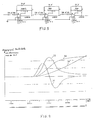
- FIG. 1 shows a static laser characteristic curve according to the prior art
- 2 shows a block diagram of the device according to the invention for regulating the bias current of a laser diode
- 3 shows an embodiment of the evaluation circuit according to the invention
- FIG. 4 shows a diagram of the signal profiles in the evaluation circuit.
- FIG. 1 shows a characteristic curve, known from the prior art, of the optical output power of a laser diode as a function of the injection current, which has a kink, the position of which can be different as a function of the temperature and due to aging.
- the kink lies in the range of the threshold current, which is subject to a variation in the specimen and to temperature and aging-related fluctuations.
- the curve shape of the characteristic curve corresponds to a hyperbola, the kink point of the characteristic curve lies at the point of maximum curvature.
- the diagram also shows the amounts of the bias current I bias and the modulation current I mod .
- the bias current is slightly above the threshold current, the fluctuation of which is compensated for by a control circuit.
- the regulation of the bias current of a laser diode is described in particular on a passive optical network.
- the laser diode 5a which interacts in a unit 5 with the monitor diode 5b, is operated with continuously increasing current from a controllable current source 23, which is based on a linear ramp signal from a ramp signal generator 21, which is zero from the time at which it is started emits a signal with a constant slope with time increasing, is controlled.
- a controlled switch 22 which can interrupt the laser bias current I bias 15, is arranged between the ramp generator 21 and the controllable current source 23. The value of the laser bias current stored in the ramp generator is retained.
- the modulation current I mod is added to the bias current I bias 15 in the adder 4.
- the output signal 16 emerging from the monitor diode 5b is fed to an evaluation circuit 6, there is threefold differentiated and the resulting signal is applied to the input of the downstream comparator 7 which, when a zero crossing occurs, outputs a control signal via line 17 to the control unit 8.
- This control unit 8 controls both the ramp generator 21 and the switch 22 and, in the presence of a blanking signal on line 9, switches off the bias current.
- An external signal on line 10 initiates the start of a new measuring ramp.
- the reset associated with the simultaneous start signal of the ramp signal generator 21 is carried out via a signal generated on the line 11 by the control unit 8, and the momentary value of the ramp signal current is stopped and thus held with a signal on line 13 also generated by the control unit.
- the ramp generator 21 is reset and started via the signal 11.
- the monitor diode 5b converts the light output of the laser diode 5a into an output signal which is differentiated three times in the evaluation circuit 6.
- the resulting signal is fed to the input of the comparator 7, which emits an output signal to the line 17 when this signal present at its input crosses zero. If this output signal is present, the control unit 8 generates a stop signal at its output 13 after a preselectable time delay, with the result that the instantaneous value of the ramp signal is retained and stored.
- the optimum value of the bias current for a control cycle is thus established and the current source 23 maintains this value until the end of the next cycle.
- this value is not lost when the switch 22 is opened via a blanking signal 9. This is done, for example, to protect the laser diode when no data is being transmitted.
- the laser threshold current can be determined without prior adjustment.
- the ideal bias current is always the same amount larger than the threshold current and can therefore be determined by the laser bias control 18 without further feedback.
- FIG. 3 shows an exemplary embodiment of the evaluation circuit 6 comprising three series-known bandpass filters of the first order, which carry out the differentiation of the signal 16 and to which the comparator 7, not shown, is connected.
- the amplification is advantageously limited to the value 10 per stage.
- the corner frequency of the filters must lie above the highest significant spectral line of the input signal 16. The derivatives of the input signal 16 are taken at the points marked C, D.E.
- the signal profiles occurring in the differentiation in the evaluation circuit 6 are shown in FIG.
- the curve 31 corresponds to the input signal 16, which is identical to the laser characteristic.
- the curves 32, 33 and 34 shown correspond to the first, second and third derivatives of the input signal 16 and were removed at the locations of the filters designated C, D, E in FIG.
- the bias current Since the laser chip is subject to temperature fluctuations, the bias current must be adjusted regularly during which the laser cannot be modulated. It is therefore advisable to provide a separate time window for the setting process in the network protocol, in which period no data transmission takes place.
Abstract
Description
Die Erfindung betrifft ein Verfahren zur Regelung des Vorstromes einer mit einer Monitordiode in einem Regelkreis mit Operationsverstärkern zusammenwirkenden Laserdiode, umfassend Signalverarbeitungsfilter, eine elektrische Versorgungseinheit, wie z.B. eine Stromquelle, und einen Nulldurchgangsdetektor sowie eine Einrichtung zur Durchführung dieses Verfahrens, mit einem Addierer zur Überlagerung des Vorstromes und eines Modulationsstromes, und einer den Vorstrom liefernden steuerbaren Stromquelle sowie einer mit der Monitordiode verbundenen Auswerteschaltung.The invention relates to a method for regulating the bias current of a laser diode interacting with a monitor diode in a control circuit with operational amplifiers, comprising signal processing filters, an electrical supply unit, such as e.g. a current source, and a zero-crossing detector and a device for carrying out this method, with an adder for superimposing the bias current and a modulation current, and a controllable current source supplying the bias current and an evaluation circuit connected to the monitor diode.
In Systemen der optischen Nachrichtentechnik hat sich die Verwendung von Halbleiterlasern als vorteilhaft erwiesen, insbesonders durch die Modulierbarkeit höherer Frequenzen sowie verlustarmer Signalübertragungen über große Übertragungslängen ohne Zwischenverstärker.The use of semiconductor lasers has proven to be advantageous in systems of optical communications technology, in particular due to the ability to modulate higher frequencies and low-loss signal transmissions over long transmission lengths without an intermediate amplifier.
Um den Halbleiter-Laser schnell modulieren zu können, muß dieser wahrend der Datenübertragung mit einem Vorstrom beaufschlagt sein, der etwas über dem Schwellstrom liegt. Zu diesem Vorstrom wird dann der Modulationsstrom addiert. Dabei müssen jedoch die durch Alterung und Temperaturschwankungen hervorgerufenen Fluktuationen des Schwellstromes durch eine Regelschaltung kompensiert werden.In order to be able to modulate the semiconductor laser quickly, it must be subjected to a bias current during data transmission which is slightly above the threshold current. The modulation current is then added to this bias current. However, the fluctuations in the threshold current caused by aging and temperature fluctuations must be compensated for by a control circuit.
Es ist üblich, durch Abtasten des Strom-Spannungsverlaufes der Laserdiode den aktuellen Schwellstrom zu ermitteln, dessen Größe als Ausgangswert für eine Regelung des Vorstromes dient (Zeitschrift Elektronik 22/85, S.91). Die Regelung hat insbesondere die Aufgabe, Maximum und Minimum der Lichtleistung bei Laserbetrieb konstant zu halten.It is common to determine the current threshold current by scanning the current-voltage curve of the laser diode, the size of which serves as an output value for regulating the bias current (Zeitschrift Elektronik 22/85, p.91). The control has in particular the task of keeping the maximum and minimum of the light output constant during laser operation.
Es ist weiters zur Messung der vom Laser emittierten Lichtleistung üblich, wie etwa in US-4,344 173, im Gehäuse einer Laserdiode eine Monitordiode zu integrieren, die einen zur optischen Laserleistung direkt proportionalen Sperrstrom liefert. Der Kopplungsgrad zwischen Laserdiode und Monitordiode und damit auch der Proportionalitatsfaktor zwischen Lichtleistung und Monitorstrom ist jedoch starker Exemplarstreuung unterworfen.It is also customary to measure the light power emitted by the laser, such as in US Pat. No. 4,344,173, to integrate in the housing of a laser diode a monitor diode which delivers a reverse current which is directly proportional to the optical laser power. However, the degree of coupling between the laser diode and the monitor diode and thus also the proportionality factor between the light output and the monitor current is subject to strong specimen scatter.
Daher muß die Vorstromregelung einer Laserdiode vor der ersten Inbetriebnahme abgeglichen werden, damit die Regelschaltung die tatsächlich abgegebene Lichtleistung erfassen kann. Die Regelung erfolgt bekannterweise entweder nach der optischen Leistung bei Betreiben der Laserdiode mit Vorstrom, wobei die Lichtleistung ohne Modulationsstrom auf einen bestimmten Wert eingestellt wird, oder nach dem Mittelwert der optischen Ausgangsleistung, der sich bei kontinuierlicher Modulation ergibt, wobei der durch die gegebene Lichtleistung in der Monitordiode erzeugte Sperrstrom mit einem Referenzwert verglichen wird (Zeitschrift Elektronik 22/85, S.91-92).Therefore, the bias current control of a laser diode must be adjusted before the first start-up, so that the control circuit can detect the light output actually emitted. As is known, the regulation takes place either according to the optical power when the laser diode is operated with bias current, the light power being set to a certain value without modulation current, or according to the mean value of the optical output power, which results from continuous modulation, the given by the given light power in the reverse current generated by the monitor diode is compared with a reference value (Zeitschrift Elektronik 22/85, p.91-92).
Diese bekannten Methoden benötigen aber zur genauen Funktion einen Abgleichvorgang, weil der Proportionalitatsfaktor zwischen optischer Leistung und Monitorstrom nicht bekannt ist.However, these known methods require an adjustment process in order to function correctly, because the proportionality factor between optical power and monitor current is not known.
Aufgabe der Erfindung ist es daher, diesen bekannten Nachteil zu vermeiden und eine Regelung vorzusehen, welche eine selbstjustierende Vorstromregelung einer Laserdiode ermöglicht.The object of the invention is therefore to avoid this known disadvantage and to provide a regulation which enables a self-adjusting bias current regulation of a laser diode.
In der US-4,344 173 wird zwar ebenfalls ein Regelkreis zum Einstellen des Vorstromes einer Laserdiode, der aus einer Stromquelle, einem Bandpaßfilter und einem Nulldurchgangsdetektor besteht, verwendet, in dieser Anordnung wird aber eine Oberwellenanalyse durchgeführt, die einen hohen Aufwand zur Folge hat.US Pat. No. 4,344,173 also describes a control circuit for setting the bias current of a laser diode, which consists of a current source, a bandpass filter and one There is a zero crossing detector, but in this arrangement a harmonic analysis is carried out, which results in a high outlay.
Die Erfindung löst die Aufgabe dadurch, daß die Laserdiode von einem von der Versorgungseinheit abgegebenen linearen Stromrampensignal betrieben wird, daß das Ausgangssignal der Monitordiode dreifach differenziert wird, und daß bei Erkennen eines Nulldurchganges des dreifach differenzierten Monitordioden-Ausgangssignals durch den Nulldurchgangsdetektor eine Optimalstromstarke des Stromrampensignalgenerators festgehalten wird.The invention achieves the object in that the laser diode is operated by a linear current ramp signal output by the supply unit, in that the output signal of the monitor diode is differentiated three times, and in that when the zero-crossing detector detects a zero crossing of the three-differentiated monitor diode output signal, an optimum current intensity of the current ramp signal generator is recorded becomes.
Vorteilhafterweise weist bei Betreiben der Laserdiode mit einem linearen Stromrampensignal ihre optische Ausgangsleistung in Abhängigkeit von der Zeit einen ihrer optischen Ausgangsleistung in Abhängigkeit des Injektionsstromes identen Verlauf auf. Dies ermöglicht eine selbsttätige Einstellung des Laservorstromes auf einen Optimalwert, der bei Nulldurchgang der dritten Ableitung der Laserleistung nach dem Strom, welche der dritten Ableitung der optischen Ausgangsleistung nach der Zeit bei Betreiben der Laserdiode mit einem linearen Rampensignal entspricht, vorliegt. Der Vorstrom-Arbeitspunkt wird somit auf den Stromwert eingestellt, bei dem die dritte Ableitung durch Null geht, wodurch ein Extremwert, in diesem Fall ein Maximum, der Krümmung der Leistungskurve charakterisiert ist.When the laser diode is operated with a linear current ramp signal, its optical output power as a function of time advantageously has a course identical to its optical output power as a function of the injection current. This enables the laser bias current to be set automatically to an optimum value which is present at zero crossing of the third derivative of the laser power after the current, which corresponds to the third derivative of the optical output power after the time when the laser diode is operated with a linear ramp signal. The bias current operating point is thus set to the current value at which the third derivative goes through zero, whereby an extreme value, in this case a maximum, is characterized in the curvature of the power curve.
In weiterer Ausgestaltung der Erfindung kann vorgesehen sein, daß die Optimalstromstärke nach einer Verzögerungszeitspanne festgehalten wird.In a further embodiment of the invention it can be provided that the optimum current strength is recorded after a delay period.
Eine derartige Verzögerungszeitspanne kann zur weiteren Abstimmung des optimalen Vorstromwerts vorteilhaft sein, da es sich aus Erfahrungswerten ergeben kann, daß ein um einen bestimmten Prozentsatz höherer Wert je nach Typ der Laserdiode besser geeignet ist.Such a delay period can be advantageous for further tuning the optimal bias current value, since experience may show that a value that is higher by a certain percentage is more suitable depending on the type of laser diode.
Die Erfindung löst die oben angegebene Aufgabe auch mittels einer Einrichtung zur Durchführung des oben genannten Verfahrens mit einem Addierer zur Überlagerung des Vorstromes und eines Modulationsstromes, und einer den Vorstrom liefernden steuerbaren Stromquelle, sowie einer mit der Monitordiode verbundenen Auswerteschaltung, welche dadurch gekennzeichnet ist, daß ein an sich bekannter Rampensignalgenerator die die Laserdiode betreibende, steuerbare Stromquelle durch ein lineares Rampensignal ansteuert, und daß die Auswerteschaltung eine das Ausgangssignal der Monitordiode dreifach differenzierende Schaltung umfaßt, die über einen den Nulldurchgang des dreifach differenzierten Monitordioden-Ausgangssignals feststellenden Komparator mit einer den Rampensignalgenerator steuerenden Steuereinheit verbunden ist.The invention also achieves the above-mentioned object by means of a device for carrying out the above-mentioned method with an adder for superimposing the bias current and a modulation current, and a controllable current source supplying the bias current, and an evaluation circuit connected to the monitor diode, which is characterized in that a known ramp signal generator which drives the controllable current source which operates the laser diode by means of a linear ramp signal, and that the evaluation circuit comprises a circuit which differentiates the output signal of the monitor diode three times and which uses a comparator which determines the zero crossing of the triple-differentiated monitor diode output signal and has a control signal generator Control unit is connected.
Ein weiteres Merkmal der Erfindung ist es, daß zwischen dem Rampengenerator und der steuerbaren Stromquelle ein mit diesen verbundener, von der Steuereinheit ansteuerbarer Schalter angeordnet ist.Another feature of the invention is that a switch connected to the ramp generator and the controllable current source and controllable by the control unit is arranged.
Dadurch kann der Laservorstrom während einer Modulationspause etwa aus Energiespargründen unterbrochen werden, ohne daß der im Rampengenerator gespeicherte, optimale Wert des Laservorstromes verlorengeht, wobei sowohl der Rampengenerator als auch der Schalter von der Steuereinheit angesteuert wird.As a result, the laser bias can be interrupted during a modulation pause, for example to save energy, without the optimal value of the laser bias stored in the ramp generator being lost, both the ramp generator and the switch being controlled by the control unit.
Ein weiteres Merkmal der Erfindung ist es, daß die Auswerteschaltung drei in Serie geschaltete, an sich bekannte aktive Filter umfaßt, denen der Komparator nachgeschaltet ist.Another feature of the invention is that the evaluation circuit comprises three active filters, known per se, which are connected in series and which are followed by the comparator.
Die Differenzierung des Ausgangssignales der Monitordiode kann damit auf einfache Weise durchgeführt werden, da die aktiven Filter im vorgegebenen Frequenzbereich wie eine Kaskade dreier Differenzierer wirken.The differentiation of the output signal of the monitor diode can thus be carried out in a simple manner, since the active filters act like a cascade of three differentiators in the predetermined frequency range.
Vorteilhafterweise werden Bandpaßfilter 1.Ordnung als die drei aktiven Filter verwendet.Advantageously, 1st order bandpass filters are used as the three active filters.
Die Erfindung wird nun anhand eines Ausführungsbeispieles unter Zuhilfenahme der angeschlossenen Zeichnungen näher beschrieben.The invention will now be described in more detail using an exemplary embodiment with the aid of the attached drawings.
Es zeigen Fig. 1 eine statische Laserkennlinie nach dem Stand der Technik; Fig.2 ein Blockschaltbild der erfindungsgemäßen Einrichtung zur Regelung des Vorstromes einer Laserdiode; Fig.3 ein Ausführungsbeispiel der erfindungsgemäßen Auswerteschaltung; und Fig.4 ein Diagramm der Signalverläufe in der Auswerteschaltung.1 shows a static laser characteristic curve according to the prior art; 2 shows a block diagram of the device according to the invention for regulating the bias current of a laser diode; 3 shows an embodiment of the evaluation circuit according to the invention; and FIG. 4 shows a diagram of the signal profiles in the evaluation circuit.
Fig.1 zeigt eine aus dem Stand der Technik bekannte Kennlinie der optischen Ausgangsleistung einer Laserdiode in Abhängigkeit vom Injektionsstrom, welche einen Knick aufweist, dessen Position in Abhängigkeit von der Temperatur sowie aufgrund der Alterung unterschiedlich sein kann. Der Knick liegt im Bereich des Schwellstromes, welcher einer Exemplarstreuung sowie temperatur- und alterungsbedingten Schwankungen unterworfen ist. Die Kurvenform der Kennlinie entspricht einer Hyperbel, der Knickpunkt der Kennlinie liegt im Punkt der maximalen Krümmung.1 shows a characteristic curve, known from the prior art, of the optical output power of a laser diode as a function of the injection current, which has a kink, the position of which can be different as a function of the temperature and due to aging. The kink lies in the range of the threshold current, which is subject to a variation in the specimen and to temperature and aging-related fluctuations. The curve shape of the characteristic curve corresponds to a hyperbola, the kink point of the characteristic curve lies at the point of maximum curvature.
Das Diagrarnm zeigt weiters die Beträge des Vorstromes Ibias sowie des Modulationsstromes Imod. Der Vorstrom liegt dabei etwas über dem Schwellstrom, dessen Fluktuation durch eine Regelschaltung kompensiert wird.The diagram also shows the amounts of the bias current I bias and the modulation current I mod . The bias current is slightly above the threshold current, the fluctuation of which is compensated for by a control circuit.
Die Regelung des Vorstromes einer Laserdiode wird insbesonders an einem passiven optischen Netzwerk beschrieben.The regulation of the bias current of a laser diode is described in particular on a passive optical network.
Fig.2 zeigt eine komplette Laservorstromregelung 18 anhand eines Blockschaltbildes. Dabei wird die in einer Einheit 5 mit der Monitordiode 5b in Wechselwirkung stehende Laserdiode 5a mit kontinuierlich ansteigendem Strom aus einer steuerbaren Stromquelle 23 betrieben, welche von einem linearen Rampensignal aus einem Rampensignalgenerator 21, der vom Zeitpunkt, an dem er gestartet wird, ein von Null mit konstanter Steigung mit der Zeit ansteigendes Signal abgibt, angesteuert wird. Zufolge dieser Schaltung entspricht die optische Ausgangsleistung in Abhängigkeit von der Zeit der optischen Ausgangsleistung in Abhängigkeit vom Injektionsstrom. Zwischen dem Rampengenerator 21 und der steuerbaren Stromquelle 23 ist ein gesteuerter Schalter 22 angeordnet, welcher den Laservorstrom Ibias 15 unterbrechen kann. Dabei bleibt der im Rampengenerator gespeicherte Wert des Laservorstromes erhalten. Zum Vorstrom Ibias 15 wird im Addierer 4 der Modulationsstrom Imod hinzuaddiert.2 shows a complete laser bias
Das aus der Monitordiode 5b austretende Ausgangssignal 16 wird einer Auswerteschaltung 6 zugeführt, dort dreifach differenziert und das daraus resultierende Signal an den Eingang des nachgeschalteten Komparator 7 gelegt, der bei Auftreten eines Nulldurchganges ein Steuersignal über die Leitung 17 an die Steuereinheit 8 abgibt. Diese Steuereinheit 8 steuert sowohl den Rampengenerator 21 alsauch den Schlater 22 und bewirkt bei Vorliegen eines Austast-Signals an der Leitung 9 das Abschalten des Vorstromes. Ein externes Signal auf Leitung 10 veranlaßt den Start einer neuen Meßrampe. Das Rücksetzen verbunden mit gleichzeitigem Startsignal des Rampensignalgenerators 21 erfolgt über ein durch die Steuereinheit 8 generiertes Signal auf der Leitung 11, das Anhalten und damit Festhalten des Augenblickwertes des Rampensignalstroms mit einem ebenfalls von der Steuereinheit erzeugtem Signal auf Leitung 13.The
Am Meßbeginn wird, bei geschlossenem Schalter 22, der Rampengenerator 21 jeweils über das Signal 11 rückgesetzt und gestartet. Das von Null an anwachsende Rampensignal des Rampensignalgenerators 21 steuert die Stromquelle 23, die einen gleichfalls ansteigenden Vorstrom zum Betreiben der Laserdiode 5a abgibt. Die Monitordiode 5b wandelt die Lichtleistung der Laserdiode 5a in ein Ausgangssignal um, welches in der Auswerteschaltung 6 dreifach differenziert wird. Das dabei entstehende Signal wird dem Eingang des Komparators 7 zugeführt, der bei einem Nulldurchgang dieses an seinem Eingang anliegenden Signals ein Ausgangssignal an die Leitung 17 abgibt. Bei Vorliegen dieses Ausgangssignals erzeugt die Steuereinheit 8 nach einer vorwahlbaren Zeitverzögerung an ihrem Ausgang 13 ein Stop-Signal, womit ein Festhalten und ein Speichern des Augenblickwertes des Rampensignals erreicht wird. Damit ist der optimale Wert des Vorstromes für einen Regeldurchlauf festgelegt und die Stromquelle 23 behält diesen Wert bis zum Ende des nächsten Durchlaufs bei. Durch das Speichern des Rampensignals geht dieser Wert auch nicht verloren, wenn über ein Austastsignal 9 der Schalter 22 geöffnet wird. Dies erfolgt beispielsweise zur Schonung der Laserdiode, wenn gerade keine Daten übertragen werden.At the start of the measurement, with the
Indem die Position des Maximums der Krümmung der Kennlinie der optischen Ausgangsleistung einer Laserdiode und damit näherungsweise auch die Position des Nulldurchganges der 3.Ableitung unabhängig von konstanten Verstärkungsfaktoren ist und die Laserdiode mit einem linearen Stromrampensignal betrieben wird, kann der Laserschwellstrom ohne vorherigen Abgleich ermittelt werden. Der ideale Vorstrom ist immer um den gleichen Betrag größer als der Schwellstrom und kann daher ohne weitere Rückmeldung von der Laservorstromregelung 18 ermittelt werden.Since the position of the maximum curvature of the characteristic curve of the optical output power of a laser diode and thus also approximately the position of the zero crossing of the third derivative is independent of constant amplification factors and the laser diode is operated with a linear current ramp signal, the laser threshold current can be determined without prior adjustment. The ideal bias current is always the same amount larger than the threshold current and can therefore be determined by the
Fig.3 zeigt ein Ausführungsbeispiel der Auswerteschaltung 6 aus drei in Serie geschalteten, an sich bekannten Bandpaßfiltern 1. Ordnung, welche die Differenzierung des Signales 16 durchführen , und an welche der nicht dargestellte Komparator 7 anschließt. Vorteilhafterweise wird zur Verringerung der Schwingungsneigung der Schaltung die Verstärkung auf den Wert 10 pro Stufe begrenzt. Um die aktiven Filter als Differenzierer mit linearem Phasengang einsetzen zu können, muß die Eckfrequenz der Filter über der höchsten signifikanten Spektrallinie des Eingangssignales 16 liegen. Die Ableitungen des Eingangssignales 16 werden an den mit C,D.E gekennzeichneten Stellen abgenommen.3 shows an exemplary embodiment of the evaluation circuit 6 comprising three series-known bandpass filters of the first order, which carry out the differentiation of the
Die bei der Differenzierung in der Auswerteschaltung 6 auftretenden Signalverläufe sind in Fig.4 dargestellt. Der Kurvenzug 31 entspricht dem Eingangssignal 16, welches mit der Laserkennlinie ident ist. Die dargestellten Kurvenzüge 32,33 und 34 entsprechen der ersten, zweiten bzw. dritten Ableitung des Eingangssignales 16 und wurden an den mit C,D,E in der Fig.4 bezeichneten Stellen der Filter abgenommen.The signal profiles occurring in the differentiation in the evaluation circuit 6 are shown in FIG. The
Es zeigt sich eine vernachlässigbare Abhängigkeit des Nulldurchganges der dritten Ableitung 34 des Eingangssignales 16 und eine geringe Beeinflussung des Signales durch Rauschen.It shows a negligible dependence of the zero crossing of the
Da der Laserchip Temperaturschwankungen unterworfen ist, muß eine regelmäßige Einstellung des Vorstromes durchgeführt werden, während der der Laser nicht moduliert werden kann. Es empfiehlt sich daher, im Protokoll des Netzwerkes ein eigenes Zeitfenster für den Einstellvorgang vorzusehen, in welchem Zeitraum keine Datenübertragung stattfindet.Since the laser chip is subject to temperature fluctuations, the bias current must be adjusted regularly during which the laser cannot be modulated. It is therefore advisable to provide a separate time window for the setting process in the network protocol, in which period no data transmission takes place.
Claims (6)
Applications Claiming Priority (2)
| Application Number | Priority Date | Filing Date | Title |
|---|---|---|---|
| AT149292 | 1992-07-21 | ||
| AT1492/92 | 1992-07-21 |
Publications (2)
| Publication Number | Publication Date |
|---|---|
| EP0580568A2 true EP0580568A2 (en) | 1994-01-26 |
| EP0580568A3 EP0580568A3 (en) | 1994-04-20 |
Family
ID=3515061
Family Applications (1)
| Application Number | Title | Priority Date | Filing Date |
|---|---|---|---|
| EP93890144A Withdrawn EP0580568A2 (en) | 1992-07-21 | 1993-07-21 | Bias power supply for laserdiode |
Country Status (2)
| Country | Link |
|---|---|
| US (1) | US5323408A (en) |
| EP (1) | EP0580568A2 (en) |
Families Citing this family (16)
| Publication number | Priority date | Publication date | Assignee | Title |
|---|---|---|---|---|
| EP0572856A1 (en) * | 1992-06-01 | 1993-12-08 | Siemens Aktiengesellschaft | Controlling of a pulsed high frequency generator, in particular for laser excitation |
| GB2281162B (en) * | 1993-08-04 | 1997-04-23 | Fulcrum Communications Limited | Optical transmitters |
| US5463648A (en) * | 1994-08-01 | 1995-10-31 | Litton Systems, Inc. | Pulse forming network for diode laser |
| US6518962B2 (en) * | 1997-03-12 | 2003-02-11 | Seiko Epson Corporation | Pixel circuit display apparatus and electronic apparatus equipped with current driving type light-emitting device |
| US20040017749A1 (en) * | 2002-07-24 | 2004-01-29 | Plasmon Lms, Inc. | Rewritable optical storage device with extended life |
| US20040257352A1 (en) * | 2003-06-18 | 2004-12-23 | Nuelight Corporation | Method and apparatus for controlling |
| US20050200296A1 (en) * | 2004-02-24 | 2005-09-15 | Naugler W. E.Jr. | Method and device for flat panel emissive display using shielded or partially shielded sensors to detect user screen inputs |
| US20050200292A1 (en) * | 2004-02-24 | 2005-09-15 | Naugler W. E.Jr. | Emissive display device having sensing for luminance stabilization and user light or touch screen input |
| US20050200294A1 (en) * | 2004-02-24 | 2005-09-15 | Naugler W. E.Jr. | Sidelight illuminated flat panel display and touch panel input device |
| CN1957471A (en) * | 2004-04-06 | 2007-05-02 | 彩光公司 | Color filter integrated with sensor array for flat panel display |
| CN1981318A (en) * | 2004-04-12 | 2007-06-13 | 彩光公司 | Low power circuits for active matrix emissive displays and methods of operating the same |
| US20050248515A1 (en) * | 2004-04-28 | 2005-11-10 | Naugler W E Jr | Stabilized active matrix emissive display |
| US20060007206A1 (en) * | 2004-06-29 | 2006-01-12 | Damoder Reddy | Device and method for operating a self-calibrating emissive pixel |
| DE102005009317B4 (en) * | 2005-02-18 | 2007-05-31 | Atmel Germany Gmbh | Method and device for determining a laser threshold of a laser diode |
| US20080273044A1 (en) * | 2007-05-02 | 2008-11-06 | Govorkov Sergei V | Semiconductor light-emitting device illuminated projection display with high grayscale resolution |
| JP2020004802A (en) * | 2018-06-26 | 2020-01-09 | 株式会社Qdレーザ | Laser driver, light source, and image projection device |
Citations (4)
| Publication number | Priority date | Publication date | Assignee | Title |
|---|---|---|---|---|
| US4344173A (en) * | 1978-09-25 | 1982-08-10 | Northern Telecom Limited | Stabilization circuit for a digitally operated laser |
| CA1210070A (en) * | 1984-10-26 | 1986-08-19 | Northern Telecom Limited | Laser transmitter |
| US4795976A (en) * | 1987-01-15 | 1989-01-03 | American Telephone And Telegraph Company At&T Bell Laboratories | Apparatus and derivative technique for testing devices |
| EP0376555A2 (en) * | 1988-12-29 | 1990-07-04 | AT&T Corp. | Laser control method and circuitry |
Family Cites Families (4)
| Publication number | Priority date | Publication date | Assignee | Title |
|---|---|---|---|---|
| US898702A (en) * | 1908-03-13 | 1908-09-15 | Ingersoll Rand Co | Hammer-drill. |
| US4680810A (en) * | 1985-06-28 | 1987-07-14 | American Telephone And Telegraph Company, At&T Bell Labs | Means for controlling a semiconductor device and communication system comprising the means |
| JPH0738478B2 (en) * | 1986-04-08 | 1995-04-26 | キヤノン株式会社 | Semiconductor laser drive device |
| JPH0361966A (en) * | 1989-07-31 | 1991-03-18 | Ricoh Co Ltd | Output controller for semiconductor laser |
-
1993
- 1993-07-20 US US08/094,841 patent/US5323408A/en not_active Expired - Fee Related
- 1993-07-21 EP EP93890144A patent/EP0580568A2/en not_active Withdrawn
Patent Citations (4)
| Publication number | Priority date | Publication date | Assignee | Title |
|---|---|---|---|---|
| US4344173A (en) * | 1978-09-25 | 1982-08-10 | Northern Telecom Limited | Stabilization circuit for a digitally operated laser |
| CA1210070A (en) * | 1984-10-26 | 1986-08-19 | Northern Telecom Limited | Laser transmitter |
| US4795976A (en) * | 1987-01-15 | 1989-01-03 | American Telephone And Telegraph Company At&T Bell Laboratories | Apparatus and derivative technique for testing devices |
| EP0376555A2 (en) * | 1988-12-29 | 1990-07-04 | AT&T Corp. | Laser control method and circuitry |
Non-Patent Citations (3)
| Title |
|---|
| HALBLEITER- SCHALTUNGSTECHNIK, SPRINGER-VERLAG BERLIN ISBN 3-540-19475-4 9. AUFLAGE, Seiten 326 - 327 U. TIETZE, CH. SCHENK * |
| PATENT ABSTRACTS OF JAPAN vol. 12, no. 108 (E-597)7. April 1988 & JP-A-62 237 786 (CANON INC) * |
| TRANSACTIONS OF THE INSTITUTE OF ELECTRONICS , INFORMATION, AND COMMUNICATION ENGINEERS OF JAPAN, (IEICE) SECTION E Bd. 73, Nr. 1 , Januar 1990 , TOKYO JP Seiten 133 - 134 M. YAMADA ET AL 'Method for estimating the threshold current level in semiconductor injection lasers' * |
Also Published As
| Publication number | Publication date |
|---|---|
| US5323408A (en) | 1994-06-21 |
| EP0580568A3 (en) | 1994-04-20 |
Similar Documents
| Publication | Publication Date | Title |
|---|---|---|
| EP0580568A2 (en) | Bias power supply for laserdiode | |
| DE69632652T2 (en) | Method and device for stabilizing a mode-locked laser | |
| DE2847182C3 (en) | Method for modulation current regulation of laser diodes | |
| EP0343725B1 (en) | Optical transmitter with a laser diode | |
| DE2652608A1 (en) | METHOD FOR REGULATING THE OUTPUT PERFORMANCE OF A SEMICONDUCTOR LASER | |
| DE2841433A1 (en) | PRE-CURRENT CONTROL OF LASER DIODES | |
| EP0625835A1 (en) | Optical transmission system with a laser diode | |
| DE19532648A1 (en) | Method and device for controlling diode-pumped solid-state lasers | |
| DE3608930A1 (en) | METHOD FOR REGULATING THE OPTICAL PERFORMANCE OF A LASER AND CIRCUIT FOR IMPLEMENTING THE METHOD | |
| DE3021119C2 (en) | Inverter circuit for operating an asynchronous motor with controllable speed | |
| EP0173155B1 (en) | Power supply for the light sources of frequency-modulated optical detectors | |
| DE3706635C2 (en) | ||
| DE3712759A1 (en) | X-RAY DIAGNOSIS DEVICE | |
| DE3421851C2 (en) | Method for regulating the wavelength and power of the output radiation of a semiconductor radiation source | |
| DE10046898B4 (en) | Method for controlling the operating point of a modulator and associated drive unit | |
| WO2024061605A1 (en) | Laser device and method | |
| EP1693935A1 (en) | Determination of the lasing threshold of a laser diode | |
| EP0141192A2 (en) | Optical transmission system with laser control | |
| DE2837728C2 (en) | ||
| DE2751286A1 (en) | CONTINUOUSLY ACTING REGULATORY ARRANGEMENT FOR STABILIZING AN ELECTRICAL SIZE | |
| DE10047380B4 (en) | Method for controlling the working range of a modulator and associated drive unit | |
| DE3048978A1 (en) | OPTICAL DATA TRANSFER SYSTEM | |
| DE3045545C2 (en) | Method for regulating the output signal of a semiconductor laser and circuit arrangement for carrying out this method | |
| DE2809234B2 (en) | Semiconductor laser modulator circuit | |
| DE4030995C2 (en) |
Legal Events
| Date | Code | Title | Description |
|---|---|---|---|
| PUAI | Public reference made under article 153(3) epc to a published international application that has entered the european phase |
Free format text: ORIGINAL CODE: 0009012 |
|
| AK | Designated contracting states |
Kind code of ref document: A2 Designated state(s): BE CH DE DK ES FR GB IT LI NL SE |
|
| PUAL | Search report despatched |
Free format text: ORIGINAL CODE: 0009013 |
|
| AK | Designated contracting states |
Kind code of ref document: A3 Designated state(s): BE CH DE DK ES FR GB IT LI NL SE |
|
| STAA | Information on the status of an ep patent application or granted ep patent |
Free format text: STATUS: THE APPLICATION IS DEEMED TO BE WITHDRAWN |
|
| 18D | Application deemed to be withdrawn |
Effective date: 19941021 |