EP0584724A2 - Parallel transmission of TDMA sync and data bursts by artificial frequency selective fade and decision feedback equalization - Google Patents
Parallel transmission of TDMA sync and data bursts by artificial frequency selective fade and decision feedback equalization Download PDFInfo
- Publication number
- EP0584724A2 EP0584724A2 EP93113274A EP93113274A EP0584724A2 EP 0584724 A2 EP0584724 A2 EP 0584724A2 EP 93113274 A EP93113274 A EP 93113274A EP 93113274 A EP93113274 A EP 93113274A EP 0584724 A2 EP0584724 A2 EP 0584724A2
- Authority
- EP
- European Patent Office
- Prior art keywords
- burst
- intermediate frequency
- tap
- signal
- data burst
- Prior art date
- Legal status (The legal status is an assumption and is not a legal conclusion. Google has not performed a legal analysis and makes no representation as to the accuracy of the status listed.)
- Granted
Links
Images
Classifications
-
- H—ELECTRICITY
- H04—ELECTRIC COMMUNICATION TECHNIQUE
- H04W—WIRELESS COMMUNICATION NETWORKS
- H04W52/00—Power management, e.g. TPC [Transmission Power Control], power saving or power classes
- H04W52/04—TPC
Definitions
- the present invention relates generally to time division multiple access transmission systems, and more specifically to a TDMA transmission system capable of high speed transmission of data and synchronization bursts higher than the operating speed of TDMA preambleless modems.
- TDMA transmission systems a succession of short-duration bursts emanating from a number of different stations is presented to a demodulator. Each burst has its own independent carrier phase and consequently rapid-acquisition modems are mandatory.
- a synchronization burst is first transmitted, followed by an information-carrying data burst.
- the synchronization burst is usually structured so that it starts with a preamble followed by a unique word and various control bits.
- the preamble contains a series of bits that accentuates carrier and clock line spectra to assist lock-up at the receive site during the training interval
- the transmission of a preamble represents a loss of transmission efficiency, and hence proposals have hitherto been made to implement preambleless modems.
- a preambleless TDMA sync burst is time-division multiplexed with a data burst of duration much longer than the duration of the sync burst, subjected to quadrature phase shift keying (QPSK) modulation upon an intermediate frequency carrier, and then to frequency translation to a microwave region for transmission.
- QPSK quadrature phase shift keying
- the transmitted bursts are frequency converted to baseband frequency, and stored into a buffer.
- a carrier and bit timing recovery circuit connected to the buffer, performs a fast Fourier transform process on the stored data burst and detects the transmitted carrier and bit timing from the data burst.
- the stored baseband signal is read out of the buffer into a QPSK demodulator where the whole contents of the original data and sync bursts are recovered collectively using what is known as an "en-block demodulation technique" and separated from each other by a time-division demultiplexer.
- the TDMA communication system of this invention attains a high level of transmission efficiency and a minimum of processing delays, not attainable with the prior art preambleless TDMA transmission, with the artificial introduction of frequency selective fade at the transmit site of the system to allow parallel transmission of sync and data bursts and the use of a decision feedback equalizer at the receive site for extracting the data burst and compensating for the distortions caused by the frequency fade.
- a time division multiplex communication system having a transmitting station and a receiving station.
- the system comprises a first modulator at the transmitting station for modulating a baseband data burst upon an intermediate frequency carrier and producing an intermediate frequency data burst having a substantially flat spectrum.
- a frequency fade circuit is provided for causing the intermediate frequency data burst to produce a spectral null in the center frequency region of its spectrum.
- a second modulator provides modulation of a baseband synchronization burst upon the intermediate frequency carrier and producing an intermediate frequency synchronization burst having a spectral energy distribution in a frequency region corresponding to the center frequency region of the intermediate frequency data burst.
- the intermediate frequency data burst having the spectral null is superimposed with the intermediate frequency synchronization burst to produce an intermediate frequency combined burst signal.
- the combined burst signal is then transmitted by a radio transmitter from the transmitting station.
- the intermediate frequency combined burst signal from the transmitting station is received by a radio receiver at the receiving station and fed into a bandpass filter having a passband corresponding to the spectral null of the intermediate frequency data burst to recover the intermediate frequency synchronization burst.
- a carrier recovery circuit is connected to the bandpass filter to recover the intermediate frequency carrier from the recovered intermediate frequency synchronization burst.
- a demodulator is connected to the bandpass filter and the carrier recovery circuit for demodulating the intermediate frequency synchronization burst with the recovered carrier to recover the baseband synchronization burst.
- a synchronous detector is connected to the radio receiver and the carrier recovery circuit for operating on the intermediate frequency combined burst signal with the recovered intermediate frequency carrier and producing a combined burst signal containing a baseband synchronization burst and a baseband data burst having a spectral null.
- a decision feedback equalizer is connected to the synchronous detector for extracting the baseband data burst having the spectral null from the combined burst signal and eliminating an intersymbol interference from the extracted baseband data burst to recover the baseband data burst having a substantially flat spectrum.
- the baseband synchronization burst has the same length of time as the baseband data burst and contains a preamble for carrier and bit timing recovery
- the frequency fade circuit comprises a delay element for introducing a delay time to the intermediate frequency data burst from the first modulator, and a subtractor.
- the intermediate frequency data burst having the spectral null is produced by the subtractor by subtracting the output of the delay element from the output of the first modulator.
- the decision feedback equalizer comprises a feedforward filter comprising first delay-line taps for receiving the output signal of the synchronous detector and producing a succession of tap signals at the first delay-line taps, first tap-gain multipliers for operating on the tap signals, and a first adder for receiving the output signal of the synchronous detector as a reference input and the tap signals from the first tap-gain multipliers and producing a feedforward output signal as said extracted baseband data burst.
- a decision circuit is included for deriving a decision output signal from an equalized signal.
- a feedback filter comprising second delay-line taps for receiving the decision output signal and producing a succession of tap signals at the second delay-line taps, second tap-gain multipliers for operating on the tap signals at the second delay-line taps, and a second adder for combining output signals from the second tap-gain multipliers to produce a feedback output signal which is combined with the feedforward signal to derive the equalized signal.
- a decision error associated with the decision circuit is detected and correlations between it and the tap signals at the first and second delay-line taps are detected for controlling the tap gains of the first and second tap-gain multipliers.
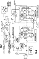
- a synchronization burst having the same duration as the data burst is generated and applied to the QPSK modulator 11 where it is modulated onto the quadrature carriers from oscillator 12.
- the sync burst contains a preamble comprising carrier and bit timing recovery (CR, BTR) fields, a unique word (UW) for burst frame synchronization, a supervisory field (SV) and the various TDMA control fields (SDC, SCA, CSC, AUX).
- the sync burst of the present invention has a lower bit rate than the data burst, and hence the modulated sync burst has a narrower spectrum at the output of modulator 11 as indicated by numeral 62 than the spectrum of the data burst.
- An adder, or multiplexer 15 is provided for multiplexing the outputs of subtractor 13 and QPSK modulator 11 in a manner similar to frequency division multiplexing.
- the narrow-band sync burst is combined with the data burst such that it occupies the center region of the data burst spectrum 61 where it is notched by the provision of the frequency fade circuit at the transmitter.
- the output of multiplexer 15 is converted to a radio frequency signal by a transmitter 16 and applied to an antenna 17 for transmission. In this way, the sync and data bursts are simultaneously transmitted.
- the transmitted burst signal is received by antenna 20 and applied to a receiver 21 where it is converted to an intermediate frequency combined burst signal, producing the same spectral energy pattern as generated at the output of the multiplexer 15 at the transmitting station.
- the sync burst Since the sync burst has a narrower bandwidth than the data burst, it can be processed as a narrow band interference signal if the data burst is treated as a desired signal and the data burst can be processed as a wideband interference signal if the sync bust is treated as a desired signal.
- the output of receiver 21 is connected to a bandpass filter 22 having a passband corresponding to the spectral energy 62 of the IF signal.
- the sync burst is extracted by bandpass filter 22.
- the extracted sync burst is applied to a carrier recovery circuit 23 and a QPSK demodulator 24.
- the transmitted carrier is recovered by carrier recovery circuit 23 from the carrier recovery field of the extracted sync burst and applied to as a local IF carrier to the QPSK demodulator 24 to demodulate the sync burst.
- a clock recovery circuit 25 is connected to the QPSK demodulator 24 to recover the transmitted clock timing from the bit timing recovery field of the extracted sync burst and deliver a sequence of bits following the bit timing recovery field.
- the intermediate frequency signal from receiver 21 is applied to a complex multiplier, or synchronous detector 26 where the sync and data bursts at baseband frequency are synchronously detected by using the quadrature carriers from the carrier recovery circuit 23.
- the output of complex multiplier 26 is applied to a decision feedback equalizer where the narrow-band interference and the intersymbol interference introduced by the artificial frequency selective fade are eliminated.
- the decision feedback equalizer comprises a feedforward filter 27, a feedback filter 28, a subtractor 29, a decision circuit 30 and an error detector 31.
- the feedforward filter 27, feedback filter 28 and decision circuit 30 are connected to clock recovery circuit 25 to operate at the recovered bit timing.
- the feedforward filter 27 comprises a four-stage shift register formed by a series of three delay-line units 401, 402 and 403, each having a symbol delay time T, forming four taps; a first (or reference) tap A at the input of delay unit 401, and second, third and fourth taps B, C and D at the outputs of delay units 401, 402 and 403, respectively.
- the output of synchronous detector 26 is connected to the input end of the delay line to produce a succession of tap signals at the taps A, B, C and D.
- the feedforward filter 27 exhibits a spectral response identical to that of the center frequency region of the notched spectral pattern 61. This is achieved by coupling the reference tap A direct to an adder 42, while coupling the taps B, C and D to complex multipliers 411, 412, and 413 whose outputs are connected to adder 42.
- a tap-gain controller 43 is connected to the taps B, C and D and to the output of error detector 31 to produce tap-gain control signals by detecting the correlations between a decision error ⁇ from the error detector 31 and the respective tap signals at the second, third and fourth delay taps.
- the tap-gain control signals are applied to the corresponding complex multipliers 41 for weighting the respective tap signals, and updated according to the least mean square (LMS) algorithm.
- LMS least mean square
- the baseband sync burst contained in the output of this synchronous detector is eliminated at the output of adder 42, producing a baseband data burst whose spectrum 61a has a spectral null in the center frequency region of the baseband frequency.
- the intersymbol interference caused by this fade can be removed by the feedback filter 28.
- the feedback filter 28 is comprised by a three-stage shift register having delay units 501, 502 and 503 with a delay time T for receiving a decision output (data burst) from the decision circuit 30 to produce a succession of tap signals.
- Complex multipliers 511, 512 and 513 are connected respectively to the outputs of delay units 501, 502 and 503 for weighting the respective tap signals with tap-gain control signals and supplying the weighted signals to an adder 52.
- These tap-gain control signals are derived by a tap-gain controller 53 which detects correlations between the decision error ⁇ and the tap signals and updates the tap-gains according to the LMS algorithm.
- An equalized data burst having a flat spectrum 60a at baseband frequencies is obtained at the output of subtractor 29 by subtracting the output of adder 52 from the output of adder 42.
- the decision circuit 30 receives the equalized data burst from subtractor 29, compares it with a predetermined decision threshold and produces a decision symbol sequence at one of four symbol values in the real and imaginary domains. This decision symbol sequence is delivered as a replica of the transmitted data burst to an external circuit, while it is reapplied to the feedback filter 28 for cancelling the intersymbol interference artificially introduced into the data burst at the transmitter.
- the artificially introduced intersymbol interference can be considered as a delayed channel response caused by interference from a symbol sequence delayed by period ⁇ , while the tap signals of the feedback filter 28 are the decision symbol sequence corresponding to that delayed response, the intersymbol interference is completely cancelled by feedback filter 28.
- the error detector 31 is connected across the input and output of the decision circuit 30 to detect an error introduced in the decision process and to update the tap-gain values of both feedforward and feedback filters. In addition to the cancellation of both sync burst interference and artificial fade distortion are eliminated, time-variant multipath fading distortions that naturally occur in the transmission route can also be cancelled by the decision feedback equalizer of this invention.
Abstract
Description
- The present invention relates generally to time division multiple access transmission systems, and more specifically to a TDMA transmission system capable of high speed transmission of data and synchronization bursts higher than the operating speed of TDMA preambleless modems.
- In TDMA transmission systems a succession of short-duration bursts emanating from a number of different stations is presented to a demodulator. Each burst has its own independent carrier phase and consequently rapid-acquisition modems are mandatory. To permit rapid acquisition of a burst, a synchronization burst is first transmitted, followed by an information-carrying data burst. The synchronization burst is usually structured so that it starts with a preamble followed by a unique word and various control bits. The preamble contains a series of bits that accentuates carrier and clock line spectra to assist lock-up at the receive site during the training interval However, the transmission of a preamble represents a loss of transmission efficiency, and hence proposals have hitherto been made to implement preambleless modems. At the transmit site of the prior art preambleless TDMA system, a preambleless TDMA sync burst is time-division multiplexed with a data burst of duration much longer than the duration of the sync burst, subjected to quadrature phase shift keying (QPSK) modulation upon an intermediate frequency carrier, and then to frequency translation to a microwave region for transmission. At the receive site, the transmitted bursts are frequency converted to baseband frequency, and stored into a buffer. A carrier and bit timing recovery circuit, connected to the buffer, performs a fast Fourier transform process on the stored data burst and detects the transmitted carrier and bit timing from the data burst. Using the recovered carrier and bit timing clock, the stored baseband signal is read out of the buffer into a QPSK demodulator where the whole contents of the original data and sync bursts are recovered collectively using what is known as an "en-block demodulation technique" and separated from each other by a time-division demultiplexer.
- However, a dramatic transmission-efficiency improvement cannot be achieved by the prior art preambleless TDMA transmission since the preamble does not accounts for a substantial portion of the sync burst. Additionally, the amount of delays introduced by the read/write operations and the en-block demodulation process cannot be ignored for high speed TDMA transmission.
- It is therefore an object of the present invention to provide a TDMA transmission technique that allows high speed transmission of bursts by parallel transmission of synchronization bursts and data bursts. The TDMA communication system of this invention attains a high level of transmission efficiency and a minimum of processing delays, not attainable with the prior art preambleless TDMA transmission, with the artificial introduction of frequency selective fade at the transmit site of the system to allow parallel transmission of sync and data bursts and the use of a decision feedback equalizer at the receive site for extracting the data burst and compensating for the distortions caused by the frequency fade.
- According to the present invention, there is provided a time division multiplex communication system having a transmitting station and a receiving station. The system comprises a first modulator at the transmitting station for modulating a baseband data burst upon an intermediate frequency carrier and producing an intermediate frequency data burst having a substantially flat spectrum. A frequency fade circuit is provided for causing the intermediate frequency data burst to produce a spectral null in the center frequency region of its spectrum. A second modulator provides modulation of a baseband synchronization burst upon the intermediate frequency carrier and producing an intermediate frequency synchronization burst having a spectral energy distribution in a frequency region corresponding to the center frequency region of the intermediate frequency data burst. The intermediate frequency data burst having the spectral null is superimposed with the intermediate frequency synchronization burst to produce an intermediate frequency combined burst signal. The combined burst signal is then transmitted by a radio transmitter from the transmitting station. The intermediate frequency combined burst signal from the transmitting station is received by a radio receiver at the receiving station and fed into a bandpass filter having a passband corresponding to the spectral null of the intermediate frequency data burst to recover the intermediate frequency synchronization burst. A carrier recovery circuit is connected to the bandpass filter to recover the intermediate frequency carrier from the recovered intermediate frequency synchronization burst. A demodulator is connected to the bandpass filter and the carrier recovery circuit for demodulating the intermediate frequency synchronization burst with the recovered carrier to recover the baseband synchronization burst. A synchronous detector is connected to the radio receiver and the carrier recovery circuit for operating on the intermediate frequency combined burst signal with the recovered intermediate frequency carrier and producing a combined burst signal containing a baseband synchronization burst and a baseband data burst having a spectral null. A decision feedback equalizer is connected to the synchronous detector for extracting the baseband data burst having the spectral null from the combined burst signal and eliminating an intersymbol interference from the extracted baseband data burst to recover the baseband data burst having a substantially flat spectrum.
- More specifically, the baseband synchronization burst has the same length of time as the baseband data burst and contains a preamble for carrier and bit timing recovery, and the frequency fade circuit comprises a delay element for introducing a delay time to the intermediate frequency data burst from the first modulator, and a subtractor. The intermediate frequency data burst having the spectral null is produced by the subtractor by subtracting the output of the delay element from the output of the first modulator.
- Preferably, the decision feedback equalizer comprises a feedforward filter comprising first delay-line taps for receiving the output signal of the synchronous detector and producing a succession of tap signals at the first delay-line taps, first tap-gain multipliers for operating on the tap signals, and a first adder for receiving the output signal of the synchronous detector as a reference input and the tap signals from the first tap-gain multipliers and producing a feedforward output signal as said extracted baseband data burst. A decision circuit is included for deriving a decision output signal from an equalized signal. A feedback filter is provided comprising second delay-line taps for receiving the decision output signal and producing a succession of tap signals at the second delay-line taps, second tap-gain multipliers for operating on the tap signals at the second delay-line taps, and a second adder for combining output signals from the second tap-gain multipliers to produce a feedback output signal which is combined with the feedforward signal to derive the equalized signal. A decision error associated with the decision circuit is detected and correlations between it and the tap signals at the first and second delay-line taps are detected for controlling the tap gains of the first and second tap-gain multipliers.
- The present invention will be described in further detail with reference to the accompanying drawings, in which:
- Fig. 1 is a block diagram of a transmitting station of a TDMA communication system of the present invention; and
- Fig. 2 is a block diagram of a receiving station of the TDMA communication system of the present invention.
- On the other hand, a synchronization burst having the same duration as the data burst is generated and applied to the
QPSK modulator 11 where it is modulated onto the quadrature carriers fromoscillator 12. As illustrated in Fig. 1, the sync burst contains a preamble comprising carrier and bit timing recovery (CR, BTR) fields, a unique word (UW) for burst frame synchronization, a supervisory field (SV) and the various TDMA control fields (SDC, SCA, CSC, AUX). Because of the equality of burst duration to the higher bit-density data burst while the total number of bits contained in the sync burst is much smaller than that of the data burst, the sync burst of the present invention has a lower bit rate than the data burst, and hence the modulated sync burst has a narrower spectrum at the output ofmodulator 11 as indicated bynumeral 62 than the spectrum of the data burst. - An adder, or
multiplexer 15 is provided for multiplexing the outputs ofsubtractor 13 andQPSK modulator 11 in a manner similar to frequency division multiplexing. Thus, the narrow-band sync burst is combined with the data burst such that it occupies the center region of thedata burst spectrum 61 where it is notched by the provision of the frequency fade circuit at the transmitter. The output ofmultiplexer 15 is converted to a radio frequency signal by atransmitter 16 and applied to anantenna 17 for transmission. In this way, the sync and data bursts are simultaneously transmitted. - At the receiving station of the TDMA transmission system, Fig. 2, the transmitted burst signal is received by
antenna 20 and applied to areceiver 21 where it is converted to an intermediate frequency combined burst signal, producing the same spectral energy pattern as generated at the output of themultiplexer 15 at the transmitting station. - Since the sync burst has a narrower bandwidth than the data burst, it can be processed as a narrow band interference signal if the data burst is treated as a desired signal and the data burst can be processed as a wideband interference signal if the sync bust is treated as a desired signal.
- The output of
receiver 21 is connected to abandpass filter 22 having a passband corresponding to thespectral energy 62 of the IF signal. Thus, the sync burst is extracted bybandpass filter 22. The extracted sync burst is applied to acarrier recovery circuit 23 and aQPSK demodulator 24. The transmitted carrier is recovered bycarrier recovery circuit 23 from the carrier recovery field of the extracted sync burst and applied to as a local IF carrier to theQPSK demodulator 24 to demodulate the sync burst. Aclock recovery circuit 25 is connected to theQPSK demodulator 24 to recover the transmitted clock timing from the bit timing recovery field of the extracted sync burst and deliver a sequence of bits following the bit timing recovery field. - The intermediate frequency signal from
receiver 21 is applied to a complex multiplier, orsynchronous detector 26 where the sync and data bursts at baseband frequency are synchronously detected by using the quadrature carriers from thecarrier recovery circuit 23. The output ofcomplex multiplier 26 is applied to a decision feedback equalizer where the narrow-band interference and the intersymbol interference introduced by the artificial frequency selective fade are eliminated. The decision feedback equalizer comprises afeedforward filter 27, afeedback filter 28, asubtractor 29, adecision circuit 30 and anerror detector 31. Thefeedforward filter 27,feedback filter 28 anddecision circuit 30 are connected toclock recovery circuit 25 to operate at the recovered bit timing. - More specifically, the
feedforward filter 27 comprises a four-stage shift register formed by a series of three delay-line units delay unit 40₁, and second, third and fourth taps B, C and D at the outputs ofdelay units synchronous detector 26 is connected to the input end of the delay line to produce a succession of tap signals at the taps A, B, C and D. - The
feedforward filter 27 exhibits a spectral response identical to that of the center frequency region of the notchedspectral pattern 61. This is achieved by coupling the reference tap A direct to anadder 42, while coupling the taps B, C and D tocomplex multipliers adder 42. A tap-gain controller 43 is connected to the taps B, C and D and to the output oferror detector 31 to produce tap-gain control signals by detecting the correlations between a decision error ε from theerror detector 31 and the respective tap signals at the second, third and fourth delay taps. The tap-gain control signals are applied to the corresponding complex multipliers 41 for weighting the respective tap signals, and updated according to the least mean square (LMS) algorithm. As a result of establishing the reference input of thefeedforward filter 27 direct from the output ofsynchronous detector 26, the baseband sync burst contained in the output of this synchronous detector is eliminated at the output ofadder 42, producing a baseband data burst whose spectrum 61a has a spectral null in the center frequency region of the baseband frequency. - Since the artificial interference yields a two-wave multipath fade model and causes artificial fade distortion to occur in the data burst at the output of
subtractor 13, the intersymbol interference caused by this fade can be removed by thefeedback filter 28. - The
feedback filter 28 is comprised by a three-stage shift register havingdelay units decision circuit 30 to produce a succession of tap signals.Complex multipliers delay units adder 52. These tap-gain control signals are derived by a tap-gain controller 53 which detects correlations between the decision error ε and the tap signals and updates the tap-gains according to the LMS algorithm. - An equalized data burst having a
flat spectrum 60a at baseband frequencies is obtained at the output ofsubtractor 29 by subtracting the output ofadder 52 from the output ofadder 42. Thedecision circuit 30 receives the equalized data burst fromsubtractor 29, compares it with a predetermined decision threshold and produces a decision symbol sequence at one of four symbol values in the real and imaginary domains. This decision symbol sequence is delivered as a replica of the transmitted data burst to an external circuit, while it is reapplied to thefeedback filter 28 for cancelling the intersymbol interference artificially introduced into the data burst at the transmitter. - Since the artificially introduced intersymbol interference can be considered as a delayed channel response caused by interference from a symbol sequence delayed by period τ, while the tap signals of the
feedback filter 28 are the decision symbol sequence corresponding to that delayed response, the intersymbol interference is completely cancelled byfeedback filter 28. - The
error detector 31 is connected across the input and output of thedecision circuit 30 to detect an error introduced in the decision process and to update the tap-gain values of both feedforward and feedback filters. In addition to the cancellation of both sync burst interference and artificial fade distortion are eliminated, time-variant multipath fading distortions that naturally occur in the transmission route can also be cancelled by the decision feedback equalizer of this invention.
Claims (4)
- A time division multiplex communication system having a transmitting station and a receiving station, comprising:
first modulator means at said transmitting station for modulating a baseband data burst upon an intermediate frequency carrier and producing an intermediate frequency data burst having a substantially flat spectrum;
frequency fade means for causing said intermediate frequency data burst to produce a spectral null in a center frequency region of the spectrum thereof;
second modulator means for modulating a baseband synchronization burst upon said carrier and producing an intermediate frequency synchronization burst having a spectral energy distribution in a frequency region corresponding to the center frequency region of said intermediate frequency data burst;
multiplexer means for combining the intermediate frequency data burst having said spectral null and said intermediate frequency synchronization burst and producing an intermediate frequency combined burst signal;
radio transmitter means for transmitting said intermediate frequency combined burst signal from said transmitting station;
radio receiver means at said receiving station for receiving the intermediate frequency combined burst signal from said transmitting station;
a bandpass filter having a passband corresponding to the spectral null of said intermediate frequency data burst, said bandpass filter being connected to said radio receiver means for recovering said intermediate frequency synchronization burst from the intermediate frequency combined burst signal;
carrier recovery means connected to said bandpass filter for recovering said intermediate frequency carrier from the intermediate frequency synchronization burst;
demodulator means connected to said bandpass filter and said carrier recovery means for demodulating said intermediate frequency synchronization burst with the recovered intermediate frequency carrier and recovering said baseband synchronization burst;
a synchronous detector connected to said radio receiver means and said carrier recovery means for operating on the intermediate frequency combined burst signal with said recovered intermediate frequency carrier and producing a baseband combined burst signal; and
a decision feedback equalizer connected to the synchronous detector for extracting a baseband data burst having a spectral null from the baseband combined burst signal and eliminating an intersymbol interference from the extracted baseband data burst to recover said baseband data burst having a substantially flat spectrum. - A time division multiplex communication system as claimed in claim 1, wherein said baseband synchronization burst has the same length of time as said baseband data burst and contains a preamble for carrier and bit timing recovery.
- A time division multiplex communication system as claimed in claims 1 or 2, wherein said frequency fade means comprises:
delay means for introducing a delay time to said intermediate frequency data burst from said first modulator means; and
subtractor means for combining the output of the delay means with the output of the first modulator means and producing said intermediate frequency data burst having said spectral null. - A time division multip!ex communication system as claimed in claims 1, 2 or 3, wherein said decision feedback equalizer comprises:
a feedforward filter comprising a first tapped delay line for receiving the output signal of said synchronous detector and defining first delay-line taps for producing a succession of tap signals at said first delay-line taps, first tap-gain multipliers for operating on the tap signals at said first delay-line taps, and first summing means for receiving the output signal of said synchronous detector as a reference input and the tap signals from said first tap-gain multipliers and producing a feedforward output signal as said extracted baseband data burst;
decision means for deriving a decision output signal from an equalized signal;
a feedback filter for operating on the decision output signal from said decision means, the feedback filter comprising a second tapped delay line defining second delay-line taps for producing a succession of tap signals at said second delay-line taps, second tap-gain multipliers for operating on the tap signals at said second delay-line taps, and second summing means for combining output signals from said second tap-gain multipliers to produce a feedback output signal;
a decision error detector for detecting a decision error between the input and output of said decision means;
first tap-gain control means for detecting correlations between the tap signals at said first delay-line taps and said decision error for controlling tap gains of said first tap-gain multipliers with the detected correlations, respectively;
second tap-gain control means for detecting correlations between the tap signals at said second delay-line taps and said decision error for controlling tap gains of said said tap-gain multipliers with the detected correlations, respectively; and
a combiner for combining the feedforward output signal and the feedback output signal and producing a combined signal and supplying the combined signal to said decision means as said equalized signal.
Applications Claiming Priority (3)
| Application Number | Priority Date | Filing Date | Title |
|---|---|---|---|
| JP4222712A JP2720721B2 (en) | 1992-08-21 | 1992-08-21 | Modem |
| JP22271292 | 1992-08-21 | ||
| JP222712/92 | 1992-08-21 |
Publications (3)
| Publication Number | Publication Date |
|---|---|
| EP0584724A2 true EP0584724A2 (en) | 1994-03-02 |
| EP0584724A3 EP0584724A3 (en) | 1996-06-05 |
| EP0584724B1 EP0584724B1 (en) | 2000-11-08 |
Family
ID=16786729
Family Applications (1)
| Application Number | Title | Priority Date | Filing Date |
|---|---|---|---|
| EP93113274A Expired - Lifetime EP0584724B1 (en) | 1992-08-21 | 1993-08-19 | Parallel transmission of TDMA sync and data bursts by artificial frequency selective fade and decision feedback equalization |
Country Status (4)
| Country | Link |
|---|---|
| US (1) | US5367536A (en) |
| EP (1) | EP0584724B1 (en) |
| JP (1) | JP2720721B2 (en) |
| DE (1) | DE69329634T2 (en) |
Cited By (2)
| Publication number | Priority date | Publication date | Assignee | Title |
|---|---|---|---|---|
| WO2000031899A1 (en) * | 1998-11-24 | 2000-06-02 | Hughes Electronics Corporation | Synchronization in mobile satellite systems using dual-chirp waveform |
| EP0709975A3 (en) * | 1994-10-31 | 2000-07-12 | Motorola, Inc. | Method and apparatus for burst detecting |
Families Citing this family (36)
| Publication number | Priority date | Publication date | Assignee | Title |
|---|---|---|---|---|
| US5602507A (en) * | 1993-11-05 | 1997-02-11 | Ntt Mobile Communications Network Inc. | Adaptive demodulating method for generating replica and demodulator thereof |
| JP3160453B2 (en) * | 1993-11-29 | 2001-04-25 | 松下電器産業株式会社 | Data receiving device |
| JP3400545B2 (en) * | 1994-06-23 | 2003-04-28 | 株式会社日立製作所 | Decision feedback type equalizer |
| US5517528A (en) * | 1994-08-02 | 1996-05-14 | International Automated Systems, Inc. | Modulation method and apparatus for digital communications |
| US5640422A (en) * | 1994-08-02 | 1997-06-17 | International Automated Systems, Inc. | Digital communications modulation method and apparatus |
| US5550596A (en) * | 1994-11-25 | 1996-08-27 | Thomson Multimedia Sa | Digital television signal processing system including a co-channel rejection filter |
| US5654955A (en) * | 1994-12-15 | 1997-08-05 | Stanford Telecommunications, Inc. | Network entry channel for CDMA systems |
| JP2697648B2 (en) * | 1994-12-26 | 1998-01-14 | 日本電気株式会社 | Decision feedback equalizer |
| JPH08213943A (en) * | 1995-01-31 | 1996-08-20 | Nec Corp | Interference compensation device |
| FI98025C (en) * | 1995-05-05 | 1997-03-25 | Nokia Mobile Phones Ltd | Wireless LAN system and receiver |
| US6775334B1 (en) * | 1998-11-03 | 2004-08-10 | Broadcom Corporation | Equalization and decision-directed loops with trellis demodulation in high definition TV |
| US6477200B1 (en) * | 1998-11-09 | 2002-11-05 | Broadcom Corporation | Multi-pair gigabit ethernet transceiver |
| US6249544B1 (en) * | 1998-11-13 | 2001-06-19 | Broadcom Corporation | System and method for high-speed decoding and ISI compensation in a multi-pair transceiver system |
| US6253345B1 (en) * | 1998-11-13 | 2001-06-26 | Broadcom Corporation | System and method for trellis decoding in a multi-pair transceiver system |
| US6201831B1 (en) * | 1998-11-13 | 2001-03-13 | Broadcom Corporation | Demodulator for a multi-pair gigabit transceiver |
| US6252904B1 (en) * | 1998-11-13 | 2001-06-26 | Broadcom Corporation | High-speed decoder for a multi-pair gigabit transceiver |
| AU2512300A (en) * | 1999-01-20 | 2000-08-07 | Broadcom Corporation | Trellis decoder with correction of pair swaps, for use in gigabit ethernet transceivers |
| US6236691B1 (en) * | 1999-03-16 | 2001-05-22 | International Automated Systems, Inc. | Signal demodulation method and apparatus |
| US6088403A (en) * | 1999-03-16 | 2000-07-11 | Johnson; Neldon P. | Signal extraction method and apparatus |
| AU4492100A (en) * | 1999-04-22 | 2000-11-10 | Broadcom Corporation | Gigabit ethernet with timing offsets between the twisted pairs |
| US7065125B1 (en) * | 1999-08-13 | 2006-06-20 | Viasat, Inc. | Method and apparatus for multiple access over a communication channel |
| US20070127553A1 (en) * | 1999-08-13 | 2007-06-07 | Viasat, Inc. | Code Reuse Multiple Access For Satellite Return Link |
| DE10024375A1 (en) * | 2000-05-17 | 2001-12-20 | Infineon Technologies Ag | Prevention of parasitic state involves introducing artificial noise signal with noise signal frequency in system processing path, e.g. so signal level exceeds threshold |
| US6973145B1 (en) | 2000-09-01 | 2005-12-06 | Ut-Battelle, Llc | Digital-data receiver synchronization method and apparatus |
| JP2002335188A (en) * | 2001-05-08 | 2002-11-22 | Sony Corp | Apparatus and method for radio transmission and for radio reception |
| JP2003069456A (en) * | 2001-08-28 | 2003-03-07 | Dx Antenna Co Ltd | Signal changeover device |
| US7177368B2 (en) * | 2001-09-26 | 2007-02-13 | General Atomics | Data transfer using frequency notching of radio-frequency signals |
| US7068950B2 (en) * | 2002-03-18 | 2006-06-27 | Lucent Technologies Inc. | Correcting misalignment between data and a carrier signal in transmitters |
| JP2003309533A (en) * | 2002-04-17 | 2003-10-31 | Matsushita Electric Ind Co Ltd | Wireless transmitter, wireless receiver, and method thereof |
| US20070197169A1 (en) * | 2006-02-01 | 2007-08-23 | Viss Marlin E | Systems and methods for transmitter and channel characterization |
| US7809054B2 (en) * | 2006-04-18 | 2010-10-05 | International Business Machines Corporation | One-sample-per-bit decision feedback equalizer (DFE) clock and data recovery |
| US20080240224A1 (en) * | 2006-04-18 | 2008-10-02 | Carballo Juan A | Structure for one-sample-per-bit decision feedback equalizer (dfe) clock and data recovery |
| US7852914B2 (en) * | 2006-12-20 | 2010-12-14 | Broadcom Corporation | Fade equalizer |
| US8341506B2 (en) * | 2007-03-30 | 2012-12-25 | HGST Netherlands B.V. | Techniques for correcting errors using iterative decoding |
| EP2091197A1 (en) * | 2008-02-15 | 2009-08-19 | Motorola, Inc., A Corporation of the State of Delaware; | Method and device for detecting a GSM channel of interest |
| US8494035B2 (en) * | 2011-03-18 | 2013-07-23 | Imec | Frequency-domain adaptive feedback equalizer |
Citations (2)
| Publication number | Priority date | Publication date | Assignee | Title |
|---|---|---|---|---|
| JPS63288544A (en) * | 1987-05-21 | 1988-11-25 | Toshiba Corp | Digital signal transmitter-receiver |
| JPH0289439A (en) * | 1988-09-27 | 1990-03-29 | Toshiba Corp | Digital radio system |
Family Cites Families (6)
| Publication number | Priority date | Publication date | Assignee | Title |
|---|---|---|---|---|
| US4675880A (en) * | 1985-05-02 | 1987-06-23 | The United States Of America As Represented By The Administrator Of The National Aeronautics And Space Administration | Antimultipath communication by injecting tone into null in signal spectrum |
| US4852090A (en) * | 1987-02-02 | 1989-07-25 | Motorola, Inc. | TDMA communications system with adaptive equalization |
| US5175747A (en) * | 1989-10-31 | 1992-12-29 | Mitsubishi Denki Kabushiki Kaisha | Equalizer |
| JP2551231B2 (en) * | 1990-11-16 | 1996-11-06 | 日本電気株式会社 | Decision feedback equalizer |
| US5274672A (en) * | 1991-10-31 | 1993-12-28 | Motorola, Inc. | Optimized clock recovery for an MSK system |
| US5241544A (en) * | 1991-11-01 | 1993-08-31 | Motorola, Inc. | Multi-channel tdm communication system slot phase correction |
-
1992
- 1992-08-21 JP JP4222712A patent/JP2720721B2/en not_active Expired - Fee Related
-
1993
- 1993-08-19 DE DE69329634T patent/DE69329634T2/en not_active Expired - Fee Related
- 1993-08-19 EP EP93113274A patent/EP0584724B1/en not_active Expired - Lifetime
- 1993-08-20 US US08/109,681 patent/US5367536A/en not_active Expired - Fee Related
Patent Citations (2)
| Publication number | Priority date | Publication date | Assignee | Title |
|---|---|---|---|---|
| JPS63288544A (en) * | 1987-05-21 | 1988-11-25 | Toshiba Corp | Digital signal transmitter-receiver |
| JPH0289439A (en) * | 1988-09-27 | 1990-03-29 | Toshiba Corp | Digital radio system |
Non-Patent Citations (2)
| Title |
|---|
| PATENT ABSTRACTS OF JAPAN vol. 013 no. 117 (E-731) ,22 March 1989 & JP-A-63 288544 (TOSHIBA CORP) 25 November 1988, * |
| PATENT ABSTRACTS OF JAPAN vol. 014 no. 282 (E-0942) ,19 June 1990 & JP-A-02 089439 (TOSHIBA CORP) 29 March 1990, * |
Cited By (3)
| Publication number | Priority date | Publication date | Assignee | Title |
|---|---|---|---|---|
| EP0709975A3 (en) * | 1994-10-31 | 2000-07-12 | Motorola, Inc. | Method and apparatus for burst detecting |
| WO2000031899A1 (en) * | 1998-11-24 | 2000-06-02 | Hughes Electronics Corporation | Synchronization in mobile satellite systems using dual-chirp waveform |
| US6418158B1 (en) | 1998-11-24 | 2002-07-09 | Hughes Electronics Corporation | Synchronization in mobile satellite systems using dual-chirp waveform |
Also Published As
| Publication number | Publication date |
|---|---|
| EP0584724B1 (en) | 2000-11-08 |
| DE69329634T2 (en) | 2001-05-03 |
| DE69329634D1 (en) | 2000-12-14 |
| EP0584724A3 (en) | 1996-06-05 |
| JPH0823360A (en) | 1996-01-23 |
| US5367536A (en) | 1994-11-22 |
| JP2720721B2 (en) | 1998-03-04 |
Similar Documents
| Publication | Publication Date | Title |
|---|---|---|
| EP0584724B1 (en) | Parallel transmission of TDMA sync and data bursts by artificial frequency selective fade and decision feedback equalization | |
| US4873683A (en) | TDMA radio system employing BPSK synchronization for QPSK signals subject to random phase variation and multipath fading | |
| JP3338747B2 (en) | Interference wave canceller | |
| EP0318685B1 (en) | Phase coherent TDMA quadrature receiver for multipath fading channels | |
| US5757853A (en) | Spread spectrum time diversity communications system | |
| EP0318684B1 (en) | Rapid reference acquisition and phase error compensation for radio transmission of data | |
| AU739837B2 (en) | A data transmission/reception unit | |
| US4281411A (en) | High speed digital communication receiver | |
| US4321705A (en) | Digital equalizer for a cross-polarization receiver | |
| JPH09116475A (en) | Time diversity transmission/reception system | |
| US5369668A (en) | Fast response matched filter receiver with decision feedback equalizer | |
| CA1210877A (en) | Method of synchronizing parallel channels of orthogonally multiplexed parallel data transmission system and improved automatic equalizer for use in such a transmission system | |
| US4757319A (en) | Adaptive depolarization-interference-compensator | |
| GB1531533A (en) | Data transmission system | |
| WO2001089165A1 (en) | Cellular communications system receivers | |
| US6075823A (en) | Apparatus and method of achieving improved diversity reception in a digital radio communications system | |
| EP0459823B1 (en) | Radio communication system | |
| EP0343189B1 (en) | Tdma communications system with adaptive equalization | |
| DK167832B1 (en) | DEVICE IN A MOBILE PHONE RECEIVER TO REDUCE BIT ERRORS | |
| EP2015468A1 (en) | Baseband combiner for digital radio links | |
| JPH0435546A (en) | Interference wave eliminating system | |
| AU678032B2 (en) | Burst differential receiver | |
| JPH0653937A (en) | Hybrid modulated wave transmission system | |
| JP2595751B2 (en) | Wireless transceiver | |
| Mourelo et al. | Adaptive DFE for GMSK in indoor radio channels |
Legal Events
| Date | Code | Title | Description |
|---|---|---|---|
| PUAI | Public reference made under article 153(3) epc to a published international application that has entered the european phase |
Free format text: ORIGINAL CODE: 0009012 |
|
| AK | Designated contracting states |
Kind code of ref document: A2 Designated state(s): DE FR GB |
|
| PUAL | Search report despatched |
Free format text: ORIGINAL CODE: 0009013 |
|
| AK | Designated contracting states |
Kind code of ref document: A3 Designated state(s): DE FR GB |
|
| 17P | Request for examination filed |
Effective date: 19960424 |
|
| GRAG | Despatch of communication of intention to grant |
Free format text: ORIGINAL CODE: EPIDOS AGRA |
|
| 17Q | First examination report despatched |
Effective date: 19990920 |
|
| GRAG | Despatch of communication of intention to grant |
Free format text: ORIGINAL CODE: EPIDOS AGRA |
|
| GRAH | Despatch of communication of intention to grant a patent |
Free format text: ORIGINAL CODE: EPIDOS IGRA |
|
| GRAH | Despatch of communication of intention to grant a patent |
Free format text: ORIGINAL CODE: EPIDOS IGRA |
|
| GRAA | (expected) grant |
Free format text: ORIGINAL CODE: 0009210 |
|
| AK | Designated contracting states |
Kind code of ref document: B1 Designated state(s): DE FR GB |
|
| REF | Corresponds to: |
Ref document number: 69329634 Country of ref document: DE Date of ref document: 20001214 |
|
| ET | Fr: translation filed | ||
| PLBE | No opposition filed within time limit |
Free format text: ORIGINAL CODE: 0009261 |
|
| STAA | Information on the status of an ep patent application or granted ep patent |
Free format text: STATUS: NO OPPOSITION FILED WITHIN TIME LIMIT |
|
| 26N | No opposition filed | ||
| REG | Reference to a national code |
Ref country code: GB Ref legal event code: IF02 |
|
| PGFP | Annual fee paid to national office [announced via postgrant information from national office to epo] |
Ref country code: FR Payment date: 20020808 Year of fee payment: 10 |
|
| PGFP | Annual fee paid to national office [announced via postgrant information from national office to epo] |
Ref country code: GB Payment date: 20020814 Year of fee payment: 10 |
|
| PGFP | Annual fee paid to national office [announced via postgrant information from national office to epo] |
Ref country code: DE Payment date: 20020829 Year of fee payment: 10 |
|
| PG25 | Lapsed in a contracting state [announced via postgrant information from national office to epo] |
Ref country code: GB Free format text: LAPSE BECAUSE OF NON-PAYMENT OF DUE FEES Effective date: 20030819 |
|
| PG25 | Lapsed in a contracting state [announced via postgrant information from national office to epo] |
Ref country code: DE Free format text: LAPSE BECAUSE OF NON-PAYMENT OF DUE FEES Effective date: 20040302 |
|
| GBPC | Gb: european patent ceased through non-payment of renewal fee |
Effective date: 20030819 |
|
| PG25 | Lapsed in a contracting state [announced via postgrant information from national office to epo] |
Ref country code: FR Free format text: LAPSE BECAUSE OF NON-PAYMENT OF DUE FEES Effective date: 20040430 |
|
| REG | Reference to a national code |
Ref country code: FR Ref legal event code: ST |