EP0587975A2 - Diversity radio receiver - Google Patents
Diversity radio receiver Download PDFInfo
- Publication number
- EP0587975A2 EP0587975A2 EP93101584A EP93101584A EP0587975A2 EP 0587975 A2 EP0587975 A2 EP 0587975A2 EP 93101584 A EP93101584 A EP 93101584A EP 93101584 A EP93101584 A EP 93101584A EP 0587975 A2 EP0587975 A2 EP 0587975A2
- Authority
- EP
- European Patent Office
- Prior art keywords
- signal
- signals
- delayed
- frequency
- digital modulated
- Prior art date
- Legal status (The legal status is an assumption and is not a legal conclusion. Google has not performed a legal analysis and makes no representation as to the accuracy of the status listed.)
- Withdrawn
Links
Images


Classifications
-
- H—ELECTRICITY
- H04—ELECTRIC COMMUNICATION TECHNIQUE
- H04B—TRANSMISSION
- H04B7/00—Radio transmission systems, i.e. using radiation field
- H04B7/02—Diversity systems; Multi-antenna system, i.e. transmission or reception using multiple antennas
- H04B7/04—Diversity systems; Multi-antenna system, i.e. transmission or reception using multiple antennas using two or more spaced independent antennas
- H04B7/08—Diversity systems; Multi-antenna system, i.e. transmission or reception using multiple antennas using two or more spaced independent antennas at the receiving station
- H04B7/0837—Diversity systems; Multi-antenna system, i.e. transmission or reception using multiple antennas using two or more spaced independent antennas at the receiving station using pre-detection combining
- H04B7/084—Equal gain combining, only phase adjustments
-
- H—ELECTRICITY
- H04—ELECTRIC COMMUNICATION TECHNIQUE
- H04L—TRANSMISSION OF DIGITAL INFORMATION, e.g. TELEGRAPHIC COMMUNICATION
- H04L1/00—Arrangements for detecting or preventing errors in the information received
- H04L1/02—Arrangements for detecting or preventing errors in the information received by diversity reception
- H04L1/06—Arrangements for detecting or preventing errors in the information received by diversity reception using space diversity
Definitions
- the present invention relates to a diversity radio receiver and, more particularly, to a reception local oscillator offset diversity radio receiver in a digital radio communication system.
- a plurality of antennas spaced apart from each other so as to decrease the spatial correlation of the reception levels are used to perform reception by switching the reception antenna to an antenna having a higher level, or space diversity for synchronizing the frequencies and phases of input RF signals, or IF frequencies.
- offset transmission diversity for modulating carrier frequencies having a predetermined difference from two or more transmission base stations with the same baseband signal, simultaneously transmitting the modulated signals, and causing one antenna at the reception unit to receive the modulated signals.
- the predetermined frequency difference between the plurality of base stations spaced apart from each other must be assured, and a circuit for minimizing a time lag between the modulation baseband signals of the respective stations is required.
- this scheme requires an implementation of circuit arrangements in both the transmission and reception units. Two or more electric waves are required in principle, thereby wasting the electric waves.
- an object of the present invention to provide a new and improved diversity radio receiver in which the plurality of electric waves which have been conventionally used need not be used, and a portable radio reception system capable of obtaining a diversity effect without requiring complicated phase control between a plurality of antennas can be realized.
- a diversity radio receiver for receiving and demodulating digital modulated signals with delayed and differential detection, the receiver comprising: a plurality of reception branch means for respectively receiving the digital modulated signals and converting received digital modulated signals into intermediate frequency signals having frequency differences having a predetermined relationship with modulation baseband signal; adding means for adding the intermediate frequency signals converted by the plurality of reception branch means; delayed and differential detection means for delaying and differentially detecting a sum signal from the adding means; and post detection filter means for filtering a signal delayed and differentially detected by the delayed and differential detection means, using a bandwidth of not less than a Nyquist frequency of the received digital modulated signals, thereby outputting demodulated signals of the received digital modulated signals.
- a diversity radio receiver for receiving and demodulating digital modulated signals with delayed and differential detection, the receiver comprising: a plurality of reception branch means for respectively receiving the digital modulated signals and converting received digital modulated signals into intermediate frequency signals having frequency differences having a predetermined relationship with a modulation baseband signal; adding means for adding the intermediate frequency signals converted by the plurality of reception branch means; delayed and differential detection means comprising a delay device for delaying a sum signal from the adding means by a predetermined time, a fist mixer for mixing the sum signal from the adding means with a signal delayed by the delay device; a phase shifter for phase-shifting the sum signal from the adding means or a delayed signal from the delay device by a predetermined phase-shifting amount; and a second mixer for mixing the sum signal from the adding means with a signal phase-shifted by the phase shifter; first and second post detection filter means for filtering signals from the first and second mixers in the delayed and differential detection means at predetermined bandwidths, respectively;
- a diversity radio receiver for receiving and demodulating digital modulated signals with delayed and differential detection, the receiver comprising: a plurality of reception branch means for respectively receiving the digital modulated signals and converting received digital modulated signals into intermediate frequency signals having frequency differences having a predetermined relationship with a modulation baseband signal; adding means for adding the intermediate frequency signals converted by the plurality of reception branch means; frequency converting means for mixing a sum signal from the adding means with a signal having a frequency equal to a nominal center frequency of the intermediate frequency signal, thereby converting the sum signal into a low-frequency band signal; baseband delayed and differential detection means for performing differential logic processing of the low-frequency band signal converted by the frequency converting means to perform baseband delayed and differential detection; and post detection filter means for filtering a signal parasychronously detected by the baseband delayed and differential detection means, at a predetermined bandwidth, thereby outputting a demodulated signal of the received digital modulated signals.
- the diversity scheme is based on the following the first principle.
- Input signals from a plurality of reception branches are converted into IF signals having frequency differences having a predetermined relationship with a modulation baseband signal, and these signals are simply added to each other.
- the resultant sum signal is delayed and differentially detected through an IF filter.
- the filtered signal passes through an appropriate bandpass filter to obtain demodulated signals.
- Fig. 1 is a block diagram of an arrangement obtained when two-branch space diversity is employed as diversity based on the first principle of the present invention.
- reference numeral 1 denotes a reception antenna in a reception branch B1; 2, a mixer for frequency conversion; 3, a reception local oscillator; 4, a bandpass filter for extracting a desired IF (intermediate frequency) signal; 5, a reception antenna in a reception branch B2; 6, a mixer for frequency conversion; 7, a reception local oscillator; 8, a bandpass filter for extracting a desired IF signal; 9, an adder for synthesizing signals from the reception branches B1 and B2; 10, an IF filter for limiting the main band; and 11, a delay device; 12, a multiplier; 13, a post detection filter; 14, a detected/reproduced signal output terminal.
- R1(t) and ⁇ 1(t) are parameters representing the fading characteristics of a radio transmission path on the reception antenna 1 side.
- the parameters R1(t) and ⁇ 1(t) are generally random variables representing a Rayleigh distribution and a uniform distribution of 0 to 2 ⁇ , respectively. These random variations cause degradation of the quality of the digital modulated signal received by the reception antenna 1.
- the above parameters are given under the assumption that no variations occur at about a modulation baud rate, i.e., the input waves are metastationary waves.
- a signal received by the reception branch B1 is converted into an IF band signal by the local oscillator 3, the mixer 2, and the bandpass filter 4.
- the nominal IF frequency of the received digital modulated signal is defined as fi
- the baud rate of the modulation baseband signal is defined as fB
- a delayed baud rate in delayed detection is defined as d
- Equation (11) The two signals represented by equations (8) and (10) are multiplied with each other by the mixer 12, and only a low-frequency component is extracted by the post detection filter 13.
- equation (11) can be generally established. That is, in this case, since m - n ⁇ d/2 is established, each of the frequencies of the third and fourth terms in equation (11) is given as (m - n)/d ⁇ fb ⁇ fB/2 where fB/2 is the Nyquist frequency of the received digital modulated signal. If the band of the post detection filter 13 has a frequency higher than the Nyquist frequency, the third and fourth terms can be eliminated, so that only the first and second terms are left.
- Equation (13) represents an equi-gain diversity output upon delayed and differential detection.
- Delayed and differential detection can be achieved with delay of a plurality of bauds and sine detection and cosine detection as detection directions.
- GMSK Gausian Filtered Minimum Shift Keying
- a receiver (first embodiment) arranged based on the principle of the present invention apparently obtains a diversity effect (i.e., a bit error rate can be reduced to about 1/10 to 1/100).
- a bandpass filter which covers the band of a composite signal obtained by adding the two reception branch signals is used as the main band limit IF filter 10.
- Fig. 4 shows a circuit arrangement of a route roll-off filter type bandpass filter arranged in each of reception branches B1 and B2 which receive ⁇ /4-shifted QPSK (Quadrature Phase Shift Keying) signal according to the second embodiment.
- QPSK Quadrature Phase Shift Keying
- reference numerals 25 and 26 denote route roll-off type bandpass filters each having an offset IF frequency as its center frequency; 15, a 1-baud delay device; 16, a ⁇ /2 phase shifter; 17, a cosine detection mixer; 18, a sine detection mixer; 19 and 20, post detection filters; 21 and 22, detected signal identification determination circuits; 23, a detection signal parallel/serial converter; and 24, a reproduced signal output terminal.
- 1-baud delayed detection is generally employed for the ⁇ /4-shifted QPSK signal. Both sine detection and cosine detection are required.
- an output from the delay device 15 is equal to the value obtained from equation (10), and an output from the adder 9 is equal to the value obtained from equation (8).
- the low-frequency component of an output from the mixer 17 is equal to the value obtained from equation (11).
- the third and fourth terms of equation (11) are AC signals of (m - n)/d ⁇ fB, and the first and second terms are baseband signals.
- the frequency of the post detection filter 19 is set the Nyquist frequency fB/2 or more, and the AC signal frequency satisfies the following condition: so that the post detection filter 19 cuts off the AC components of the third and fourth terms of equation (11), but filters the baseband signals of the first and second terms therethrough.
- An output from the post detection filter 19 is the value from equation (13).
- the present invention has the second principle that input signals from a plurality of reception branches are converted into IF signals having frequency differences having a predetermined relationship with a modulation baseband signal, these signals are simply added to each other, the resultant sum signal is delayed and differentially detected through an IF filter, and the filtered signal passes through an appropriate bandpass filter to obtain demodulated signals.
- Fig. 5 is a block diagram showing an arrangement when 2-branch space diversity is employed as diversity on the basis of the second principle of the present invention.
- Reference numeral 1 denotes an antenna of a branch B1; 2, a frequency conversion mixer; 3, a reception local oscillator; 4, a bandpass filter for extracting a desired IF frequency; 5, an antenna of a branch B2; 6, a frequency conversion mixer; 7, a reception local oscillator; 8, a bandpass filter for extracting a desired IF frequency; 9, an adder for synthesizing signals from the branches B1 and B2; 110, a frequency converter for baseband differential detection; 111, a local oscillator for baseband differential detection; 112, a baseband delay logic circuit (see Fig. 6 of the fourth embodiment for further details); 113, a post detection filter; 114, a decision circuit.
- the parameters R1(t) and ⁇ 1(t) are generally random variables representing a Rayleigh distribution and a uniform distribution of 0 to 2 ⁇ , respectively. As described above these parameters represent change in rate which is not almost changed at about a modulation baud rate of the transmission signal.
- a signal received by the reception branch B1 is converted into an IF band signal by the local oscillator 3, the mixer 2, and the bandpass filter 4. Assume that the nominal IF frequency is defined as fi, and that an offset amount of the local oscillation frequency from the nominal frequency is defined as ⁇ f1.
- r i2 (t) R2(t)/2 ⁇ cos ⁇ 2 ⁇ (f i + ⁇ f2)+ ⁇ (t)+ ⁇ 2(t) ⁇ (29)
- the adder 9 simply adds the values obtained from equations (28) and (29) to produce a composite signal ri(t) as follows:
- the nominal center frequency of the IF band is fi.
- Equation (45) represents an equi-gain diversity output upon delayed cosine detection
- equation (46) represents an equi-gain diversity output upon delayed sine detection.
- Fig. 6 shows a circuit arrangement when the present invention is applied to a multivalue modulated signal such as a QPSK signal or a ⁇ /4-shifted QPSK signal.
- Reference numeral 115 denotes a ⁇ /2 phase shifter; 116, a mixer for performing frequency conversion along the cosine axis as one of the two orthogonal directions; 117, an image cutoff filter; 118, a mixer for performing frequency conversion along the sine axis as the other one of the two orthogonal directions; 119, an image cut-off filter; 120 and 121, delay devices for a delay logic circuit 112; 122, 123, 124, and 125, multipliers for performing multiplications; 126, a adder; 127, a post detection filter; 128, a decision circuit 129, a cosine detection output terminal; 130, an adder for adding inputs after the polarity of one of the inputs is inverted; 131, a post detection filter; 132, a decision circuit; and 133
- the delay times of the delay devices 120 and 121 are set at predetermined values, and an output signal from the output terminal 129 or 133 is used as a modulated signal in correspondence with the detection axis.
- reception quality can be improved by a diversity effect without modifying the transmission unit, without using a plurality of electric waves, and without using a complicated phase control synchronization technique.
- a diversity radio receiver for receiving a digital modulated signal and demodulating the modulated signal in accordance with delayed and differential detection, wherein input signals from a plurality of reception branches are converted into IF signals having frequency differences having a predetermined relationship with a modulation baseband signal, the IF signals are added to each other, a sum signal is delayed and differentially detected through an IF filter, and a demodulated signal is obtained through a filter having a predetermined bandwidth.
- a diversity radio receiver for receiving a digital modulated signal and demodulating the modulated signal in accordance with delayed and differential detection, wherein integers are assigned to a plurality of reception branches so that differences between the integers are equal to or larger than a value obtained by dividing a delay baud count in delayed detection by 2, the baud rates of the modulation baseband signals are multiplied with amounts divided by the delay baud count in the delayed and differential detection, frequencies obtained by adding these products to the nominal IF frequencies are defined as IF frequency bands of the plurality of branches, signals converted to these IF frequency bands are added, delay operations are performed by predetermined times and phase amounts so as to perform the delayed and differential detection, and a demodulated signal is obtained through a post detection filter having a bandwidth of at least the Nyquist frequency or more.
- reception quality can be improved by a diversity effect without modifying the transmission unit, without using a plurality of electric waves, and without using a complicated phase control synchronizing technique.
- the diversity circuit can be easily formed into an IC or LSI.
- a diversity radio receiver for transmitting or receiving a digital signal to perform delayed and differential detection, wherein when signals from a plurality of reception branches are to be converted into IF band signals, the input signals are converted into the IF band signals such that differences as amounts of an integer multiple of a value obtained by dividing the modulation baud rate of the transmission digital signal by the delay baud count are obtained, and the differences are the Nyquist frequency or more, the converted IF band signals are filtered through a proper bandpass filter, the filtered signals are added to each other to obtain a sum, the sum is frequency-converted into a low-frequency signal by using a local oscillation signal having a nominal center frequency of the IF band as the signal frequency, thereby performing so-called baseband delayed and differential detection for performing differential logic processing in this band, and then the detected signal is filtered through a proper baseband filter having at least the Nyquist bandwidth, thereby reproducing the transmitted signal.
Abstract
Description
- The present invention relates to a diversity radio receiver and, more particularly, to a reception local oscillator offset diversity radio receiver in a digital radio communication system.
- In digital radio communication and particularly mobile communication, it is not easy to always assure communication quality due to the presence of fading. For this reason, diversity techniques have been frequently used.
- For example, a plurality of antennas spaced apart from each other so as to decrease the spatial correlation of the reception levels are used to perform reception by switching the reception antenna to an antenna having a higher level, or space diversity for synchronizing the frequencies and phases of input RF signals, or IF frequencies. Alternatively, offset transmission diversity for modulating carrier frequencies having a predetermined difference from two or more transmission base stations with the same baseband signal, simultaneously transmitting the modulated signals, and causing one antenna at the reception unit to receive the modulated signals.
- In the former diversity scheme, since a circuit for comparing the two reception levels and a circuit for selecting a signal on the basis of the comparison result are required, or a circuit for detecting the difference of frequencies and phases between input signals and a circuit for adjusting them to be null, the circuit arrangement is undesirably complicated.
- On the other hand, in the latter diversity scheme, the predetermined frequency difference between the plurality of base stations spaced apart from each other must be assured, and a circuit for minimizing a time lag between the modulation baseband signals of the respective stations is required. In addition, this scheme requires an implementation of circuit arrangements in both the transmission and reception units. Two or more electric waves are required in principle, thereby wasting the electric waves.
- It is, therefore, an object of the present invention to provide a new and improved diversity radio receiver in which the plurality of electric waves which have been conventionally used need not be used, and a portable radio reception system capable of obtaining a diversity effect without requiring complicated phase control between a plurality of antennas can be realized.
- It is another object of the present invention to provide a radio reception system wherein a plurality of electric waves need not be used, a diversity effect can be obtained without modifying a transmission unit and without any complexity in phase control between a plurality of antennas, and a diversity system can be easily formed into an IC or LSI.
- According to a first aspect of the present invention, there is provided a diversity radio receiver for receiving and demodulating digital modulated signals with delayed and differential detection, the receiver comprising:
a plurality of reception branch means for respectively receiving the digital modulated signals and converting received digital modulated signals into intermediate frequency signals having frequency differences having a predetermined relationship with modulation baseband signal;
adding means for adding the intermediate frequency signals converted by the plurality of reception branch means;
delayed and differential detection means for delaying and differentially detecting a sum signal from the adding means; and
post detection filter means for filtering a signal delayed and differentially detected by the delayed and differential detection means, using a bandwidth of not less than a Nyquist frequency of the received digital modulated signals, thereby outputting demodulated signals of the received digital modulated signals. - According to a second aspect of the present invention, there is provided a diversity radio receiver for receiving and demodulating digital modulated signals with delayed and differential detection, the receiver comprising:
a plurality of reception branch means for respectively receiving the digital modulated signals and converting received digital modulated signals into intermediate frequency signals having frequency differences having a predetermined relationship with a modulation baseband signal;
adding means for adding the intermediate frequency signals converted by the plurality of reception branch means;
delayed and differential detection means comprising a delay device for delaying a sum signal
from the adding means by a predetermined time, a fist mixer for mixing the sum signal from the adding means with a signal delayed by the delay device;
a phase shifter for phase-shifting the sum signal from the adding means or a delayed signal from the delay device by a predetermined phase-shifting amount; and
a second mixer for mixing the sum signal from the adding means with a signal phase-shifted by the phase shifter;
first and second post detection filter means for filtering signals from the first and second mixers in the delayed and differential detection means at predetermined bandwidths, respectively; and parallel/serial converting means for converting parallel signals respectively filtered by the first and second post detection filter means into a serial signal, thereby outputting a reproduced signal of the received digital modulated signal. - According to a third aspect of the present invention, there is provided a diversity radio receiver for receiving and demodulating digital modulated signals with delayed and differential detection, the receiver comprising:
a plurality of reception branch means for respectively receiving the digital modulated signals and converting received digital modulated signals into intermediate frequency signals having frequency differences having a predetermined relationship with a modulation baseband signal;
adding means for adding the intermediate frequency signals converted by the plurality of reception branch means;
frequency converting means for mixing a sum signal from the adding means with a signal having a frequency equal to a nominal center frequency of the intermediate frequency signal, thereby converting the sum signal into a low-frequency band signal;
baseband delayed and differential detection means for performing differential logic processing of the low-frequency band signal converted by the frequency converting means to perform baseband delayed and differential detection; and
post detection filter means for filtering a signal parasychronously detected by the baseband delayed and differential detection means, at a predetermined bandwidth, thereby outputting a demodulated signal of the received digital modulated signals. - This invention can be more fully understood from the following detailed description when taken in conjunction with the accompanying drawings, in which:
- Fig. 1 is a block diagram showing a basic circuit arrangement according to an embodiment of the present invention;
- Fig. 2 is a graph showing characteristics obtained when the present invention is applied to two-baud (two-bit) delayed cosine detection of a GMSK signal for m = 1 and n = -1;
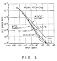
- Fig. 3 is a graph showing characteristics obtained when the present invention is applied to two-bit delayed cosine detection of the GMSK signal for n = -1 and m = 1, n = 0 and m = 2, and n = 1 and m = 3;
- Fig. 4 is a block diagram showing a basic arrangement obtained when the present invention is applied to delayed detection of a π/4-shifted QPSK signal;
- Fig. 5 is a block diagram showing a basic circuit arrangement according to another embodiment of the present invention; and
- Fig. 6 is a block diagram showing a basic circuit arrangement when the present invention is applied to delayed detection of a QPSK or π/4-shifted QPSK signal.
- Reference will now be made in detail to the presently preferred embodiments of the invention as illustrated in the accompanying drawings, in which like reference characters designate like or corresponding parts throughout the several drawings.
- In order to achieve the above objects of the present invention, the diversity scheme is based on the following the first principle. Input signals from a plurality of reception branches are converted into IF signals having frequency differences having a predetermined relationship with a modulation baseband signal, and these signals are simply added to each other. The resultant sum signal is delayed and differentially detected through an IF filter. The filtered signal passes through an appropriate bandpass filter to obtain demodulated signals.
- The first embodiment of the present invention will be described in detail with reference to the accompanying drawings.
- Fig. 1 is a block diagram of an arrangement obtained when two-branch space diversity is employed as diversity based on the first principle of the present invention.
- Referring to Fig. 1,
reference numeral 1 denotes a reception antenna in a reception branch B1; 2, a mixer for frequency conversion; 3, a reception local oscillator; 4, a bandpass filter for extracting a desired IF (intermediate frequency) signal; 5, a reception antenna in a reception branch B2; 6, a mixer for frequency conversion; 7, a reception local oscillator; 8, a bandpass filter for extracting a desired IF signal; 9, an adder for synthesizing signals from the reception branches B1 and B2; 10, an IF filter for limiting the main band; and 11, a delay device; 12, a multiplier; 13, a post detection filter; 14, a detected/reproduced signal output terminal. - Assume that a carrier frequency of a received signal is given as fc and that an angle-modulated signal representing information is given as φ(t). In this case, an input signal r1(t) from the
reception antenna 1 from the reception branch B1 is represented as follows:

where R₁(t) and ϑ₁(t) are parameters representing the fading characteristics of a radio transmission path on thereception antenna 1 side. The parameters R₁(t) and ϑ₁(t) are generally random variables representing a Rayleigh distribution and a uniform distribution of 0 to 2π, respectively. These random variations cause degradation of the quality of the digital modulated signal received by thereception antenna 1. The above parameters are given under the assumption that no variations occur at about a modulation baud rate, i.e., the input waves are metastationary waves. - Input signals from the
reception antenna 5 in the reception branch B2 are also represented as follows:

Parameters R₂(t) and ϑ₂(t) in equation (2) have characteristics similar to those of the parameters R₁(t) and ϑ₁(t), as a matter of course. - A signal received by the reception branch B1 is converted into an IF band signal by the
local oscillator 3, themixer 2, and thebandpass filter 4. Assume that the nominal IF frequency of the received digital modulated signal is defined as fi, that the baud rate of the modulation baseband signal is defined as fB, and a delayed baud rate in delayed detection (to be described later) is defined as d, the frequency of the signal converted to an IF band in the reception branch B1 is represented as follows:

The frequency of the signal converted to the IF band in the reception branch B2 is represented as follows:

where m and n are integers which satisfy the following condition:

The signals converted to the IF band signals of equations (1) and (2) by equations (3) to (5) are represented as follows:


Since a signal ri(t) synthesized by theadder 9 is the sum of the values of equations (6) and (7), the following equation is derived:


This signal is delayed and differentially detected by the delay device 11 and themixer 12 through the main band limit IFfilter 10. Since the fading parameters are not almost changed with about a delay time τ on the order of the baud rate of the modulated signal, the following equations are obtained:
A signal delayed by a delay time τ by the delay device 11 is given as follows:


Since the baud period is 1/fB, if a delay baud count is d, τ = d/fB is established. The two signals represented by equations (8) and (10) are multiplied with each other by themixer 12, and only a low-frequency component is extracted by thepost detection filter 13. The extracted component v(t) is given as follows:


The third and fourth terms of equation (11) represent AC signals of (m-n)/d·fB. Although the third and fourth terms in equation (11) have opposite signs, the negative frequency term is folded by the zero frequency to finally become the same frequency as the positive frequency. For this reason, if condition m > n is established, equation (11) can be generally established. That is, in this case, since m - n ≧ d/2 is established, each of the frequencies of the third and fourth terms in equation (11) is given as (m - n)/d·fb ≧ fB/2 where fB/2 is the Nyquist frequency of the received digital modulated signal. If the band of thepost detection filter 13 has a frequency higher than the Nyquist frequency, the third and fourth terms can be eliminated, so that only the first and second terms are left. The resultant equation is given as vd(t) as follows:


Since m and n are integers, the following equation is defined:


Equation (13) represents an equi-gain diversity output upon delayed and differential detection. - Delayed and differential detection can be achieved with delay of a plurality of bauds and sine detection and cosine detection as detection directions. When delayed and differential detection for the plurality of bauds is to be performed, a corresponding number is set in d in τ = d/fB. Detection operations in the two different directions are performed as follows:


If sine and cosine detection values are negative, they can be processed through a polarity inverter. Both equations (14) and (15) are used for a signal requiring detection in orthogonal directions. - Fig. 2 shows the experimental result obtained in two-baud (two-bit) delayed cosine detection (m = 1 and n = -1) of a GMSK (Gaussian Filtered Minimum Shift Keying) signal having a transmission band limit BbT = 0.25 at various fading pitches.
- Fig. 3 shows the experimental result for n = -1 and m = 1, n = 0 and m = 2, and n = 1 and m = 3 at a fading pitch of 10 Hz.
- As shown in Figs. 2 and 3, as compared with the absence of diversity, a receiver (first embodiment) arranged based on the principle of the present invention apparently obtains a diversity effect (i.e., a bit error rate can be reduced to about 1/10 to 1/100).
- In this experiment, a bandpass filter which covers the band of a composite signal obtained by adding the two reception branch signals is used as the main band limit IF
filter 10. However, it is possible to optimally set the bands of thefilters IF filter 10. - Fig. 4 shows a circuit arrangement of a route roll-off filter type bandpass filter arranged in each of reception branches B1 and B2 which receive π/4-shifted QPSK (Quadrature Phase Shift Keying) signal according to the second embodiment.
- Referring to Fig. 4,
reference numerals - 1-baud delayed detection is generally employed for the π/4-shifted QPSK signal. Both sine detection and cosine detection are required.
- The same reference numerals as in Fig. 1 denote the same parts in Fig. 4, and a detailed description thereof will be omitted.
- An operation of the arrangement in Fig. 4 will be described below.
- In this case, a received signal is given by equation (15):

Since delayed and differential detection may be performed for a


If the circuit is adjusted so as to establish φk - φk-1 = Δφk and 2πfcτ = 0 (mod 2π), the following relation is obtained:

If the circuit is adjusted so as to establish φk - φk-1 = Δφk and 2πfcτ = -π/2 (mod 2π), the following relation is obtained:

Substitutions of modulation phase amounts π/4, 3π/4, -3π/4, -π/4 on the transmission side into Δφk yield values (only signs are taken into consideration) in the following table.
- In the above table, if "+" is caused to correspond to 0, and "-" is caused to correspond to 1, symbolic series Xk and Yk contained in the received signal are reproduced. If these series are processed through the parallel/
serial converter 23, the original serial signal series can be restored. - Referring to Fig. 4, an output from the
delay device 15 is equal to the value obtained from equation (10), and an output from theadder 9 is equal to the value obtained from equation (8). The low-frequency component of an output from themixer 17 is equal to the value obtained from equation (11). The third and fourth terms of equation (11) are AC signals of (m - n)/d·fB, and the first and second terms are baseband signals. The frequency of thepost detection filter 19 is set the Nyquist frequency fB/2 or more, and the AC signal frequency satisfies the following condition:
so that thepost detection filter 19 cuts off the AC components of the third and fourth terms of equation (11), but filters the baseband signals of the first and second terms therethrough. - An output from the
post detection filter 19 is the value from equation (13). Cosine detection as the detecting operation of themixer 17 indicates that {2πd·fi}/fB = 0 (mod π) in equation (13), so that an output of equation (15) is obtained. - An output from the
other mixer 18 performs sine detection of a signal obtained by phase-shifting the delayed signal by ±π/2 by the phase shifter. This operation is equivalent to an operation of
post detection filter 20 is represented by equation (15). If the sampling time is given as t = kT, i.e., φk Δ φ(kt), equation (14) is rewritten as follows:
and equation (15) is also rewritten as follows:
The correspondence in the above table can be established, thereby reproducing the original signal series. This is performed in the detectedsignal decision circuits - In order to solve the conventional problems, the present invention has the second principle that input signals from a plurality of reception branches are converted into IF signals having frequency differences having a predetermined relationship with a modulation baseband signal, these signals are simply added to each other, the resultant sum signal is delayed and differentially detected through an IF filter, and the filtered signal passes through an appropriate bandpass filter to obtain demodulated signals.
- The third embodiment based on the second principle of the present invention will be described with reference to the accompanying drawings.
- Fig. 5 is a block diagram showing an arrangement when 2-branch space diversity is employed as diversity on the basis of the second principle of the present invention.
Reference numeral 1 denotes an antenna of a branch B1; 2, a frequency conversion mixer; 3, a reception local oscillator; 4, a bandpass filter for extracting a desired IF frequency; 5, an antenna of a branch B2; 6, a frequency conversion mixer; 7, a reception local oscillator; 8, a bandpass filter for extracting a desired IF frequency; 9, an adder for synthesizing signals from the branches B1 and B2; 110, a frequency converter for baseband differential detection; 111, a local oscillator for baseband differential detection; 112, a baseband delay logic circuit (see Fig. 6 of the fourth embodiment for further details); 113, a post detection filter; 114, a decision circuit. - If a carrier frequency is defined as fc and an angle-modulated signal is defined as φ(t), an angle-modulated transmission signal s(t) is expressed as follows:

The signal s(t) is transmitted, and a signal r1(t) received at thereception antenna 1 of the reception branch B1 is given as follows:

where R₁(t) and ϑ₁(t) are parameters representing the fading characteristics of a radio transmission path on thereception antenna 1 side. The parameters R₁(t) and ϑ₁(t) are generally random variables representing a Rayleigh distribution and a uniform distribution of 0 to 2π, respectively. As described above these parameters represent change in rate which is not almost changed at about a modulation baud rate of the transmission signal. - An input signal at the
reception antenna 5 of the reception branch B2 can be similarly represented as follows:

Parameters R₂(t) and ϑ₂(t) in equation (24) have characteristics similar to those of the parameters R₁(t) and ϑ₁(t), as a matter of course. A signal received by the reception branch B1 is converted into an IF band signal by thelocal oscillator 3, themixer 2, and thebandpass filter 4. Assume that the nominal IF frequency is defined as fi, and that an offset amount of the local oscillation frequency from the nominal frequency is defined as δf1. In this case, a frequency fi1 converted to the IF band in the reception branch B1 is expressed as follows:

A frequency fi2 converted into the IF band in the reception branch B2 is similarly defined as follows:

The signals converted to the IF bands are represented as follows:
In Reception Branch B1:

In Reception Branch B2:

Theadder 9 simply adds the values obtained from equations (28) and (29) to produce a composite signal ri(t) as follows:
The nominal center frequency of the IF band is fi. Therefore, a signal from the local oscillator 111 for converting the composite signal to a low-frequency band can be expressed as follows:

Θ is the phase term of the local oscillation signal. An output low-frequency component D(t) from thefrequency converter 110 is obtained from equations (30) and (31) as follows:


If Θ = 0 (mod 2π), then an in-phase component I(t) of the cosine output can be obtained as follows:


Similarly, if Θ = π/2 (mod 2π), an orthogonal component Q(t) of the sine output is obtained as follows:


Equations (33) and (34) are calculated by the basebanddelay logic circuit 112. As described above, equations (33) and (34) can be rewritten using equations (19) as follows:


A signal obtained by delaying the time τ is given from equations (35) and (36) as follows:


Similarly, an orthogonal component Q(t-τ) is given as follows:


The following logic processing using equations (35), (36), (37), and (38) is performed:


post detection filter 113, only the first and second terms are left in equations (39) and (40), thereby assuring the necessary spectral components:


If the delay baud count is defined as d, the delay time τ of thedelay logic circuit 112 is given as


in this case, since τ = d/fB, then

that is, since


Equation (45) represents an equi-gain diversity output upon delayed cosine detection, and equation (46) represents an equi-gain diversity output upon delayed sine detection. When a signal of a modulated signal of binary differential coding is to be delayed and detected, the output from equation (45) or (46) is used in accordance with the necessary detection direction, thereby obtaining diversity-processed demodulated output of the received signal. When a modulated signal of multivalue differential coding is to be delayed and differentially detected, both outputs from equations (45) and (46) are used to obtain a diversity output. - Fig. 6 shows a circuit arrangement when the present invention is applied to a multivalue modulated signal such as a QPSK signal or a π/4-shifted QPSK signal.
Reference numeral 115 denotes a π/2 phase shifter; 116, a mixer for performing frequency conversion along the cosine axis as one of the two orthogonal directions; 117, an image cutoff filter; 118, a mixer for performing frequency conversion along the sine axis as the other one of the two orthogonal directions; 119, an image cut-off filter; 120 and 121, delay devices for adelay logic circuit 112; 122, 123, 124, and 125, multipliers for performing multiplications; 126, a adder; 127, a post detection filter; 128, adecision circuit 129, a cosine detection output terminal; 130, an adder for adding inputs after the polarity of one of the inputs is inverted; 131, a post detection filter; 132, a decision circuit; and 133, a sine detection output terminal. In the QPSK or π/4-shifted QPSK signal scheme, when parallel signals from theoutput terminal 129 and theother output terminal 133 are converted into a serial signal to obtain a desired demodulated signal. - When the present invention is applied to a signal for performing binary modulation upon differential coding, such as a BPSK or GMSK (including MSK) signal, the delay times of the
delay devices 120 and 121 are set at predetermined values, and an output signal from theoutput terminal - When offset values δf₁ and δf₂ from the nominal IF frequencies of the reception
local oscillators

the converted frequencies of the first and second terms of equations (31) and (32) become equal to each other. If frequencies are different from each other, a roll-off transmission system is arranged in units of branches, or an inexpensive filter for only cutting off the image is used as each offilters frequency converter 110 and thedelay logic circuit 112. In Fig. 6, each of thefilters - As has been described with reference to the experimental results, when a receiver arrangement according to the first principle of the present invention is used, reception quality can be improved by a diversity effect without modifying the transmission unit, without using a plurality of electric waves, and without using a complicated phase control synchronization technique.
- According to the first principle of the present invention, there is provided a diversity radio receiver for receiving a digital modulated signal and demodulating the modulated signal in accordance with delayed and differential detection, wherein input signals from a plurality of reception branches are converted into IF signals having frequency differences having a predetermined relationship with a modulation baseband signal, the IF signals are added to each other, a sum signal is delayed and differentially detected through an IF filter, and a demodulated signal is obtained through a filter having a predetermined bandwidth.
- According to the first principle of the present invention, there is also provided a diversity radio receiver for receiving a digital modulated signal and demodulating the modulated signal in accordance with delayed and differential detection, wherein integers are assigned to a plurality of reception branches so that differences between the integers are equal to or larger than a value obtained by dividing a delay baud count in delayed detection by 2, the baud rates of the modulation baseband signals are multiplied with amounts divided by the delay baud count in the delayed and differential detection, frequencies obtained by adding these products to the nominal IF frequencies are defined as IF frequency bands of the plurality of branches, signals converted to these IF frequency bands are added, delay operations are performed by predetermined times and phase amounts so as to perform the delayed and differential detection, and a demodulated signal is obtained through a post detection filter having a bandwidth of at least the Nyquist frequency or more.
- As has been described, according to the second principle of the present invention, when a receiver arrangement according to the present invention is used, reception quality can be improved by a diversity effect without modifying the transmission unit, without using a plurality of electric waves, and without using a complicated phase control synchronizing technique. In addition, since processing is performed with the baseband, the diversity circuit can be easily formed into an IC or LSI.
- According to the second principle of the present invention, there is also provided a diversity radio receiver for transmitting or receiving a digital signal to perform delayed and differential detection, wherein when signals from a plurality of reception branches are to be converted into IF band signals, the input signals are converted into the IF band signals such that differences as amounts of an integer multiple of a value obtained by dividing the modulation baud rate of the transmission digital signal by the delay baud count are obtained, and the differences are the Nyquist frequency or more, the converted IF band signals are filtered through a proper bandpass filter, the filtered signals are added to each other to obtain a sum, the sum is frequency-converted into a low-frequency signal by using a local oscillation signal having a nominal center frequency of the IF band as the signal frequency, thereby performing so-called baseband delayed and differential detection for performing differential logic processing in this band, and then the detected signal is filtered through a proper baseband filter having at least the Nyquist bandwidth, thereby reproducing the transmitted signal.
Claims (18)
- A diversity radio receiver for receiving and demodulating digital modulated signals with delayed and differential detection, characterized by said receiver comprising:
a plurality of reception branch means (B1, B2) for respectively receiving the digital modulated signals and converting received digital modulated signals into intermediate frequency signals having frequency differences having a predetermined relationship with a modulation baseband signal;
adding means (9) for adding the intermediate frequency signals converted by said plurality of reception branch means (B1, B2);
delayed and differential detection means (11, 12) for delaying and differentially detecting a sum signal from said adding means (9); and
post detection filter means (13) for filtering a signal delayed and detected by said delayed and differential detection means (11, 12), using a bandwidth of not less than a Nyquist frequency of the received digital modulated signals, thereby outputting demodulated signals of the received digital modulated signals. - A receiver according to claim 1, characterized in that said plurality of reception branch means (B1, B2) include filters (4, 8) for cutting off image signals in corresponding branches.
- A receiver according to claim 1, characterized by further comprising main band limit intermediate frequency filter means (10), arranged between said adding means (9) and said delayed and differential detection means (11, 12), for filtering a composite signal from said adding means (9) at a bandwidth which covers a band of the composite signal and supplying a filtered composite signal to said delayed and differential detection means.
- A receiver according to claim 1, characterized in that each of said plurality of reception branch means (B1, B2) comprises:
a reception antenna (1, 5) for receiving the digital modulated signals transmitted as modulation signals of a predetermined carrier wave;
a local oscillator (3, 7) for outputting a local oscillation signal for converting the digital modulated signals received by said reception antenna (1, 5) into an intermediate frequency signal having a frequency difference having a predetermined relationship with a modulation baseband signal thereof;
a mixer (2, 6) for mixing the digital modulated signals received by said reception antenna (1, 5) with the local oscillation signal output from said local oscillator (3, 7); and
a bandpass filter (4, 8) for filtering a signal from said mixer at a predetermined bandwidth, thereby outputting the intermediate frequency signal. - A receiver according to claim 1, characterized in that said delayed and differential detection means (11, 12) comprises a delay device (11) for delaying the sum signal from said adding means (9) by a predetermined time, and a mixer (12) for mixing the sum signal from said adding means (9) with a signal delayed by said delay device (11).
- A receiver according to claim 1, characterized in that said plurality of reception branch means (B1, B2) set the frequency differences having the predetermined relationship so as to satisfy the following equations if the frequencies of the intermediate frequency signals are given as fi1 and fi2:


wherefi: a nominal intermediate frequency of the received digital modulated signals,fB: a baud rate of the modulation baseband signal,d: a delay baud count of said delayed and differential detection means (11, 12), andm, n: integers satisfying m ∼ n ≧ d/2 (wherein ∼ represents a subtraction). - A receiver according to claim 1, characterized in that the digital modulation signal includes a GMSK signal.
- A diversity radio receiver for receiving and demodulating digital modulated signals with delayed and differential detection, characterized by said receiver comprising:
a plurality of reception branch means (B1, B2) for respectively receiving the digital modulated signals and converting received digital modulated signals into intermediate frequency signals having frequency differences having a predetermined relationship with a modulation baseband signal;
adding means (9) for adding the intermediate frequency signals converted by said plurality of reception branch means;
delayed and differential detection means comprising:
a delay device (15) for delaying a sum signal from said adding means (9) by a predetermined time,
a fist mixer (17) for mixing the sum signal from said adding means (9) with a signal delayed by said delay device (15);
a phase shifter (16) for phase-shifting the sum signal from said adding means (9) or a delayed signal from said delay device (15) by a predetermined phase-shifting amount; and
a second mixer (18) for mixing the sum signal from said adding means (9) with a signal phase-shifted by said phase shifter (16);
first and second post detection filter means (19, 20) for filtering signals from said first and second mixers (17, 18) in said delayed and differential detection means at predetermined bandwidths,
respectively; and
parallel/serial converting means (23) for converting parallel signals respectively filtered by said first and second post detection filter means (19, 20) into a serial signal, thereby outputting a reproduced signal of the received digital modulated signal. - A receiver according to claim 8, characterized in that each of said plurality of reception branch means (B1, B2) comprises:
a reception antenna (1, 5) for receiving the digital modulated signal transmitted as a modulation signal of a predetermined carrier wave;
a local oscillator (3, 7) for outputting a local oscillation signal for converting the digital modulated signal received by said reception antenna (1, 5) into an intermediate frequency signal having a frequency difference having a predetermined relationship with a modulation baseband signal thereof;
a mixer (2, 6) for mixing the digital modulated signals received by said reception antenna with the local oscillation signal output from said local oscillator; and
a bandpass filter (25, 26) for filtering a signal from said mixer (2, 6) at a predetermined bandwidth, thereby outputting the intermediate frequency signal. - A receiver according to claim 9, characterized in that the digital modulated signals include π/4-shifted OPSK signals, and said bandpass filter includes a route roll-off filter.
- A diversity radio receiver for receiving and demodulating digital modulated signals with delayed and differential detection, characterized by said receiver comprising:
a plurality of reception branch means (B1, B2) for respectively receiving the digital modulated signals and converting received digital modulated signals into intermediate frequency signals having frequency differences having a predetermined relationship with a modulation baseband signal;
adding means (9) for adding the intermediate frequency signals converted by said plurality of reception branch means (B1, B2);
frequency converting means (110) for mixing a sum signal from said adding means (9) with a signal having a frequency equal to a nominal center frequency of the intermediate frequency signal, thereby converting the sum signal into a low-frequency band signal;
baseband delayed and differential detection means (112) for performing differential logic processing of the low-frequency band signal converted by said frequency converting means (110) to perform baseband delayed and differential detection; and
post detection filter means (113) for filtering a signal detected by said baseband delayed and differential detection means (112), at a predetermined bandwidth, thereby outputting a demodulated signal of the received digital modulated signals. - A receiver according to claim 11, characterized in that each of said plurality of reception branch means (B1, B2) comprises:
a reception antenna (1, 5) for receiving the digital modulated signals transmitted as modulation signals of a predetermined carrier wave;
a local oscillator (3, 7) for outputting a local oscillation signal for converting the digital modulated signals received by said reception antenna (1, 5) into an intermediate frequency signal having a frequency difference having a predetermined relationship with a modulation baseband signal thereof;
a mixer (2, 6) for mixing the digital modulated signals received by said reception antenna (1, 5) with the local oscillation signal output from said local oscillator (3, 7); and
a bandpass filter (4, 8) for filtering a signal from said mixer at a predetermined bandwidth, thereby outputting the intermediate frequency signal. - A receiver according to claim 11, characterized in that said plurality of reception branch means (B1, B2) set the frequency differences having the predetermined relationship so as to satisfy the following equations if the frequencies of the intermediate frequency signals are given as fi1 and fi2:


wherefi: a nominal intermediate frequency of the received digital modulated signals,fB: a baud rate of the modulation baseband signal,d: a delay baud count of said delayed and differential detection means (112), andm, n: integers satisfying m ∼ n ≧ d/2 (wherein ∼ represents a subtraction)so that the frequency difference is set to be not less than a Nyquist frequency of the received digital modulated signal. - A receiver according to claim 11, characterized in that the predetermined bandwidth in said post detection filter means (113) includes at least a Nyquist bandwidth of the received digital modulated signal.
- A receiver according to claim 11, characterized in that said frequency converting means (110) comprises:
a local oscillator (111) for outputting a local oscillation signal having a frequency equal to a nominal center frequency of the intermediate frequency signal;
phase-shifting means (115) for phase-shifting the local oscillation signal from said local oscillator (111) by π/2;
a first mixer (116) for mixing the sum signal from said adding means (9) with the local oscillation signal from said local oscillator (111); and
a second mixer (118) for mixing the sum signal from said adding means (9) with a π/2-phase-shifted signal from said phase-shifting means. - A receiver according to claim 15, characterized in that said baseband delayed and differential detection means (112) comprises:
first and second delay devices (120, 121) for delaying output signals from said first and second mixers (116, 118) by predetermined times, respectively;
first to fourth (122-125) multipliers for mutually multiplying the output signals from said first and second mixers (116, 118) and output signals from said first and second delay devices (120, 121); and
first and second adders (126, 130) for adding outputs from said first and third multipliers (122, 124) and output from said second and polarity inverted output from fourth multipliers (123, 125), respectively. - A receiver according to claim 16, characterized in that said post detection filter means (113) comprises first and second post detection filters (127, 131) for filtering outputs from said first and second adders, respectively.
- A receiver according to claim 17, characterized by further comprising first and second filters (117, 119) arranged to cut off images included in the output signals from said first and second mixers (116, 118), respectively.
Applications Claiming Priority (2)
| Application Number | Priority Date | Filing Date | Title |
|---|---|---|---|
| JP4240856A JPH0690225A (en) | 1992-09-09 | 1992-09-09 | Diversity radio receiver |
| JP240856/92 | 1992-09-09 |
Publications (2)
| Publication Number | Publication Date |
|---|---|
| EP0587975A2 true EP0587975A2 (en) | 1994-03-23 |
| EP0587975A3 EP0587975A3 (en) | 1995-11-02 |
Family
ID=17065732
Family Applications (1)
| Application Number | Title | Priority Date | Filing Date |
|---|---|---|---|
| EP93101584A Withdrawn EP0587975A3 (en) | 1992-09-09 | 1993-02-02 | Diversity radio receiver |
Country Status (3)
| Country | Link |
|---|---|
| US (1) | US5448602A (en) |
| EP (1) | EP0587975A3 (en) |
| JP (1) | JPH0690225A (en) |
Cited By (1)
| Publication number | Priority date | Publication date | Assignee | Title |
|---|---|---|---|---|
| AU759599B2 (en) * | 1998-09-25 | 2003-04-17 | Nec Corporation | Radio receiver |
Families Citing this family (38)
| Publication number | Priority date | Publication date | Assignee | Title |
|---|---|---|---|---|
| AU682700B2 (en) * | 1993-06-21 | 1997-10-16 | Kabushiki Kaisha Toshiba | Digital radio communication equipment |
| US5684836A (en) | 1994-12-22 | 1997-11-04 | Mitsubishi Denki Kabushiki Kaisha | Receiver with automatic frequency control |
| US5918154A (en) * | 1995-08-23 | 1999-06-29 | Pcs Wireless, Inc. | Communications systems employing antenna diversity |
| JP3451178B2 (en) * | 1997-05-19 | 2003-09-29 | 富士通株式会社 | Space diversity receiver |
| US6317466B1 (en) | 1998-04-15 | 2001-11-13 | Lucent Technologies Inc. | Wireless communications system having a space-time architecture employing multi-element antennas at both the transmitter and receiver |
| US6061551A (en) | 1998-10-21 | 2000-05-09 | Parkervision, Inc. | Method and system for down-converting electromagnetic signals |
| US6091940A (en) | 1998-10-21 | 2000-07-18 | Parkervision, Inc. | Method and system for frequency up-conversion |
| US6694128B1 (en) | 1998-08-18 | 2004-02-17 | Parkervision, Inc. | Frequency synthesizer using universal frequency translation technology |
| US7515896B1 (en) | 1998-10-21 | 2009-04-07 | Parkervision, Inc. | Method and system for down-converting an electromagnetic signal, and transforms for same, and aperture relationships |
| US6813485B2 (en) | 1998-10-21 | 2004-11-02 | Parkervision, Inc. | Method and system for down-converting and up-converting an electromagnetic signal, and transforms for same |
| US7039372B1 (en) | 1998-10-21 | 2006-05-02 | Parkervision, Inc. | Method and system for frequency up-conversion with modulation embodiments |
| US6560301B1 (en) | 1998-10-21 | 2003-05-06 | Parkervision, Inc. | Integrated frequency translation and selectivity with a variety of filter embodiments |
| US6061555A (en) | 1998-10-21 | 2000-05-09 | Parkervision, Inc. | Method and system for ensuring reception of a communications signal |
| US6542722B1 (en) | 1998-10-21 | 2003-04-01 | Parkervision, Inc. | Method and system for frequency up-conversion with variety of transmitter configurations |
| US6049706A (en) | 1998-10-21 | 2000-04-11 | Parkervision, Inc. | Integrated frequency translation and selectivity |
| US7236754B2 (en) | 1999-08-23 | 2007-06-26 | Parkervision, Inc. | Method and system for frequency up-conversion |
| US6370371B1 (en) | 1998-10-21 | 2002-04-09 | Parkervision, Inc. | Applications of universal frequency translation |
| US6704558B1 (en) | 1999-01-22 | 2004-03-09 | Parkervision, Inc. | Image-reject down-converter and embodiments thereof, such as the family radio service |
| US6704549B1 (en) | 1999-03-03 | 2004-03-09 | Parkvision, Inc. | Multi-mode, multi-band communication system |
| US6853690B1 (en) | 1999-04-16 | 2005-02-08 | Parkervision, Inc. | Method, system and apparatus for balanced frequency up-conversion of a baseband signal and 4-phase receiver and transceiver embodiments |
| US6879817B1 (en) | 1999-04-16 | 2005-04-12 | Parkervision, Inc. | DC offset, re-radiation, and I/Q solutions using universal frequency translation technology |
| US7952511B1 (en) | 1999-04-07 | 2011-05-31 | Geer James L | Method and apparatus for the detection of objects using electromagnetic wave attenuation patterns |
| US7065162B1 (en) | 1999-04-16 | 2006-06-20 | Parkervision, Inc. | Method and system for down-converting an electromagnetic signal, and transforms for same |
| US7693230B2 (en) | 1999-04-16 | 2010-04-06 | Parkervision, Inc. | Apparatus and method of differential IQ frequency up-conversion |
| US7110444B1 (en) | 1999-08-04 | 2006-09-19 | Parkervision, Inc. | Wireless local area network (WLAN) using universal frequency translation technology including multi-phase embodiments and circuit implementations |
| US8295406B1 (en) | 1999-08-04 | 2012-10-23 | Parkervision, Inc. | Universal platform module for a plurality of communication protocols |
| DE19942944A1 (en) * | 1999-09-08 | 2001-03-22 | Infineon Technologies Ag | Communication system and corresponding recipient |
| US7010286B2 (en) | 2000-04-14 | 2006-03-07 | Parkervision, Inc. | Apparatus, system, and method for down-converting and up-converting electromagnetic signals |
| US7454453B2 (en) | 2000-11-14 | 2008-11-18 | Parkervision, Inc. | Methods, systems, and computer program products for parallel correlation and applications thereof |
| US7072427B2 (en) | 2001-11-09 | 2006-07-04 | Parkervision, Inc. | Method and apparatus for reducing DC offsets in a communication system |
| US6985698B2 (en) * | 2001-11-14 | 2006-01-10 | Koninklijke Philips Electronics N.V. | Impedeance matching circuit for a multi-band radio frequency device |
| US7460584B2 (en) | 2002-07-18 | 2008-12-02 | Parkervision, Inc. | Networking methods and systems |
| US7379883B2 (en) | 2002-07-18 | 2008-05-27 | Parkervision, Inc. | Networking methods and systems |
| US7327994B2 (en) * | 2004-11-04 | 2008-02-05 | Hamid Rafati | Architecture for multiple-antenna systems |
| CN2749181Y (en) * | 2004-12-28 | 2005-12-28 | 精恒科技集团有限公司 | Multi-antenna receiving and transmitting processor |
| US8548407B2 (en) * | 2011-08-15 | 2013-10-01 | Delphi Technologies, Inc. | Apparatus to communicate multiple signals from multiple antennas on a single cable |
| MY182777A (en) * | 2014-10-31 | 2021-02-05 | Ericsson Telefon Ab L M | Radio receiver, method of detecting an obtruding signal in the radio receiver, and computer program |
| CN111313942A (en) * | 2020-02-12 | 2020-06-19 | 惠州Tcl移动通信有限公司 | MIMO system, method for distinguishing signals by MIMO system and mobile terminal thereof |
Citations (2)
| Publication number | Priority date | Publication date | Assignee | Title |
|---|---|---|---|---|
| US3743941A (en) * | 1971-10-28 | 1973-07-03 | Bell Telephone Labor Inc | Diversity receiver suitable for large scale integration |
| US4715048A (en) * | 1986-05-02 | 1987-12-22 | Canadian Patents And Development Limited | Frequency offset diversity receiving system |
-
1992
- 1992-09-09 JP JP4240856A patent/JPH0690225A/en active Pending
-
1993
- 1993-01-29 US US08/010,886 patent/US5448602A/en not_active Expired - Fee Related
- 1993-02-02 EP EP93101584A patent/EP0587975A3/en not_active Withdrawn
Patent Citations (2)
| Publication number | Priority date | Publication date | Assignee | Title |
|---|---|---|---|---|
| US3743941A (en) * | 1971-10-28 | 1973-07-03 | Bell Telephone Labor Inc | Diversity receiver suitable for large scale integration |
| US4715048A (en) * | 1986-05-02 | 1987-12-22 | Canadian Patents And Development Limited | Frequency offset diversity receiving system |
Cited By (1)
| Publication number | Priority date | Publication date | Assignee | Title |
|---|---|---|---|---|
| AU759599B2 (en) * | 1998-09-25 | 2003-04-17 | Nec Corporation | Radio receiver |
Also Published As
| Publication number | Publication date |
|---|---|
| JPH0690225A (en) | 1994-03-29 |
| EP0587975A3 (en) | 1995-11-02 |
| US5448602A (en) | 1995-09-05 |
Similar Documents
| Publication | Publication Date | Title |
|---|---|---|
| EP0587975A2 (en) | Diversity radio receiver | |
| KR960002933B1 (en) | Digital modulator | |
| US5787123A (en) | Receiver for orthogonal frequency division multiplexed signals | |
| JP2643792B2 (en) | Demodulator | |
| KR960003786B1 (en) | Baseband phase modulator employing digital technique | |
| US9473236B2 (en) | Relay apparatus, relay satellite, and satellite communication system | |
| US7551666B2 (en) | Wireless communications system and wireless digital receiver for use therein | |
| US5920595A (en) | Inter-cross wave compensation method and apparatus performing frequency conversion on signed not detected by a demodulating unit | |
| EP0807344B1 (en) | Method and apparatus for generating plural quadrature modulated carriers | |
| US4493099A (en) | FM Broadcasting system with transmitter identification | |
| JPH08316873A (en) | Time division multiplex fdd radio equipment and time division multiplex fdd/tdd dual mode radio equipment | |
| EP0099113B2 (en) | Interference cancellation type space diversity system | |
| JP3350068B2 (en) | Digital modulation wave demodulator | |
| JP3383318B2 (en) | Digital modulation wave demodulator | |
| US5592507A (en) | Intermediate relay station of a digital microwave communication system using service channel for monitoring and controlling space and/or time diversity, heterodyne relay, phase control, frequency control, with phase shift keying modulation | |
| JP2004241886A (en) | Frequency control circuit, radio transmission and reception device using same, and its frequency control method | |
| JPH10210092A (en) | Phase detection circuit | |
| JPH09130440A (en) | Detection circuit device | |
| JPH07183831A (en) | Digital communication method and digital communication equipment | |
| JPH0767091B2 (en) | Diversity radio receiver | |
| KR860000232B1 (en) | Compatible am stereo broadcast system | |
| JPH066397A (en) | Delay detector | |
| KR100285756B1 (en) | Apparatus for tracking carrier in wireless transfer system | |
| JPH0399549A (en) | Radio equipment for digital communication | |
| JP3287721B2 (en) | Communication device |
Legal Events
| Date | Code | Title | Description |
|---|---|---|---|
| PUAI | Public reference made under article 153(3) epc to a published international application that has entered the european phase |
Free format text: ORIGINAL CODE: 0009012 |
|
| 17P | Request for examination filed |
Effective date: 19930202 |
|
| AK | Designated contracting states |
Kind code of ref document: A2 Designated state(s): DE FR GB |
|
| PUAL | Search report despatched |
Free format text: ORIGINAL CODE: 0009013 |
|
| AK | Designated contracting states |
Kind code of ref document: A3 Designated state(s): DE FR GB |
|
| 17Q | First examination report despatched |
Effective date: 19990916 |
|
| STAA | Information on the status of an ep patent application or granted ep patent |
Free format text: STATUS: THE APPLICATION IS DEEMED TO BE WITHDRAWN |
|
| 18D | Application deemed to be withdrawn |
Effective date: 20000127 |