EP0593046B1 - Huffman code decoding circuit - Google Patents
Huffman code decoding circuit Download PDFInfo
- Publication number
- EP0593046B1 EP0593046B1 EP93116585A EP93116585A EP0593046B1 EP 0593046 B1 EP0593046 B1 EP 0593046B1 EP 93116585 A EP93116585 A EP 93116585A EP 93116585 A EP93116585 A EP 93116585A EP 0593046 B1 EP0593046 B1 EP 0593046B1
- Authority
- EP
- European Patent Office
- Prior art keywords
- bits
- bit
- address
- code
- huffman code
- Prior art date
- Legal status (The legal status is an assumption and is not a legal conclusion. Google has not performed a legal analysis and makes no representation as to the accuracy of the status listed.)
- Expired - Lifetime
Links
Images


Classifications
-
- H—ELECTRICITY
- H03—ELECTRONIC CIRCUITRY
- H03M—CODING; DECODING; CODE CONVERSION IN GENERAL
- H03M7/00—Conversion of a code where information is represented by a given sequence or number of digits to a code where the same, similar or subset of information is represented by a different sequence or number of digits
- H03M7/30—Compression; Expansion; Suppression of unnecessary data, e.g. redundancy reduction
- H03M7/40—Conversion to or from variable length codes, e.g. Shannon-Fano code, Huffman code, Morse code
- H03M7/42—Conversion to or from variable length codes, e.g. Shannon-Fano code, Huffman code, Morse code using table look-up for the coding or decoding process, e.g. using read-only memory
- H03M7/425—Conversion to or from variable length codes, e.g. Shannon-Fano code, Huffman code, Morse code using table look-up for the coding or decoding process, e.g. using read-only memory for the decoding process only
-
- H—ELECTRICITY
- H03—ELECTRONIC CIRCUITRY
- H03M—CODING; DECODING; CODE CONVERSION IN GENERAL
- H03M7/00—Conversion of a code where information is represented by a given sequence or number of digits to a code where the same, similar or subset of information is represented by a different sequence or number of digits
- H03M7/30—Compression; Expansion; Suppression of unnecessary data, e.g. redundancy reduction
- H03M7/40—Conversion to or from variable length codes, e.g. Shannon-Fano code, Huffman code, Morse code
-
- G—PHYSICS
- G06—COMPUTING; CALCULATING OR COUNTING
- G06T—IMAGE DATA PROCESSING OR GENERATION, IN GENERAL
- G06T9/00—Image coding
- G06T9/005—Statistical coding, e.g. Huffman, run length coding
-
- H—ELECTRICITY
- H03—ELECTRONIC CIRCUITRY
- H03M—CODING; DECODING; CODE CONVERSION IN GENERAL
- H03M13/00—Coding, decoding or code conversion, for error detection or error correction; Coding theory basic assumptions; Coding bounds; Error probability evaluation methods; Channel models; Simulation or testing of codes
- H03M13/65—Purpose and implementation aspects
- H03M13/6502—Reduction of hardware complexity or efficient processing
Definitions
- the present invention relates to a Huffman code decoding circuit for decoding a huffman code. More specifically, the invention relates to a Huffman code decoding circuit to be used for data compression in an image compression processing system or so forth and is capable of realizing improvement for decoding process speed and integration.
- Conventional huffman code decoding circuit employs a memory having an address for a maximum code address or a circuit for tracking a decoding tree for each bit in order to attribute a decoded word corresponding to the Huffman code.
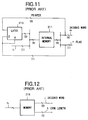
- Fig. 11 is a block diagram showing another conventional Huffman code. As shown in Fig. 11, the decoding circuit performs decoding process by tracking a decoding tree for each bit.
- the decoding circuit has a latch 210 and an internal memory 211.
- the internal memory 211 is of construction of 512 W x 9 bits.
- a leading one bit of a Huffman code data sequence is input as a least significant address, and 8 bits of an output of the latch circuit 210 is also input as upper 8 bits of the address.
- the latch circuit 210 latches a pointer when the pointer is output from the internal memory 211.
- 8 bit expresses a decoded word or the pointer., and remaining one bit is "1" if the output is the decoded word and "0" if the output is the pointer.
- a memory address is determined based on 1 bit input from the Huffman code data sequence to obtain the output of the internal memory 211.
- the output result is the pointer
- the internal memory 211 is again accessed based on the pointer and the next 1 bit of the Huffman code data sequence.
- the output is the decoded word, one cycle of decoding process is finished.
- Such circuit to perform decoding by tracking the decoding tree for each bit, memory access for the times corresponding to number of code bits to lower decoding process speed.
- FIG. 12 A further example of the Huffman code decoding circuit, in which the decoding process speed is improved, is illustrated in Fig. 12.
- the shown Huffman code decoding circuit has a memory 219 having address with a length corresponding to the maximum code length.
- This memory 219 has a construction of 64 kW x 13 bits.
- the Huffman code data sequence is input to an address input of the memory 219.
- a decoded word and a code length are obtained as the output of the memory 219 corresponding to the address.
- the maximum code length is 16 bits and the decoded word is 8 bits
- the 8 bits of the decoded word and 5 bits code length For instance, the decoded word for "all of addresses "01010 ... 0" ⁇ "01011...1" A and the code length "4" are set.
- for each address is set with respect to the Huffman code for each decoded word.
- the Huffman code decoding circuit at first, 16 bits from the leading bit of the Huffman code data sequence is input to the address in the memory 219. Assuming that "0101.." is transmitted, “0101 !, “0101” is input to the 4 upper bits of the memory 219, and a Huffman code is input to the 12 lower bits. As set forth above, since the decoded word "A” and the code length "4" are set are set in respective addresses “01010 ... 0" ⁇ "01011...1", the decoded word "A” and the code length "4" can be derived. With the code length "4", the leading bit of the Huffman code and 16 bits is determined and then the 16 bits are input to the address of the memory 219. In the similar manner, decoding process is repeated.
- the process speed may be improved.
- the maximum code length is 16 bits, it requires the memory size to be 65536 W. Therefore, when it is caused to causes increasing of the area and cost.
- the conventional Huffman code decoding circuit in which a method for providing a plurality of memory for accessing simultaneously and selecting the decoded word is employed.
- the construction of this type of the Huffman code decoding circuit is illustrated in Fig. 13.
- the shown decoding circuit includes a memory 301 ⁇ 309 taking the leading 15 bits so that 14th ⁇ 8th bits, 13th ⁇ 7th bits, 12th ⁇ 6th bits, 11th ⁇ 5th, 10th ⁇ 4th bits, 9th ⁇ 3rd bits, 8th ⁇ 2nd bits, 7th ⁇ 1st bits and 7th ⁇ 0th being taken as address inputs relative to the 16 bits of 15th ⁇ 0th bits.
- This circuit utilizes the fact that when number of word of the Huffman code is less than or equal to 256 words, and when "0" is present in the data sequence of the code, number of bits following the relevant bit is less than or equal to 7 bits.
- respective 8 bits decoded words and 4 bits code length are set in memories 301 ⁇ 309.
- the memory 301 is set the decoded word and the code length in the case of the decoded word representative of the Huffman code having "0" in the leading bit. For instance, if the Huffman code corresponding to the decoded word "A” is "0001", the decoded word "A” and the code length "4" are set for all of addresses "00100000” ⁇ "00111111” of the memory 301.
- the memory 302 is set the decoded word and the code length in the case of the decoded word representative of the Huffman code having "0" in the second leading bit. For instance, if the Huffman code corresponding to the decoded word "B" is "10011", the decoded word “B” and the code length "5" are set for all of addresses "01100000” ⁇ "01111111” of the memory 302. Subsequently, in the similar manner, when a pattern of the data sequence is a sequence, in which "0” is added for the trailing end of a sequence of "1” containing i (integer) -1 in number of "1", the decoded word and the code length are set in the first memory. On the other hand, all of the leading 8 bits are "1", i.e. "11111111” , the decoded word and the code length are set for the memory 309.
- the select signal generating portion 402 feeds a select signal for selecting the output of the memory 301 to the selector 401 when the leading bit, i.e. 15th bit of the data sequence is "0".
- the code length "4" of the 1st memory 301 output from the selector 401 us fed to the Huffman code data sequence.
- the leading end of the next Huffman code data sequence is determined.
- the decoding process is performed in the similar manner.
- Variable-length code-words are divided into two parts, a variable-length prefix part and the remainder of the code-word which is of fixed-length or approximately so.
- the variable-length part consists of a series of 1's terminated by a single 0 bit, the number of 1's preceding the first 0 bit indicates the prefix of a particular code-word.
- the code-words are arranged so that the ones with the same prefix have the same length, or as close as possible. With this codification, decoding the variable-length code-words is accomplished in two simple steps.
- the decoder determines the position of the first 0 bit in the present code-word, using this information to specify a section of the main memory.
- the second step is to index into that memory section using the remaining part of that code-word, and this retrieve the fixed length representation.
- a second object of the present invention is to provide a Huffman code decoding circuit which permits selection of various decoding systems in consideration of speeding of the decoding process and downsizing of a memory.
- a third object of the invention is to provide a Huffman code decoding circuit which can reduce a chip area in integration and lower a cost.
- the first embodiment of the Huffman code decoding circuit generally comprises a memory 10, a latch circuit 11 with a reset function and a selector 12.
- the memory 10 has a construction of 512 W (word) x 9 bits. This memory 10 has addresses of 9 bits. A leading 1 bit of a Huffman code data sequence d is input as the least significant bit (lowermost address AL). On the other hand, 3 bits of the output of the selector 12 is output as 4 bits from 2nd bit of an address (intermediate address AHL). Among 8 bits as the output of the latch circuit 11, upper 5 bits are input as upper 5 bits (upper address AHH).
- the memory 10 expresses a decoded word a and a code length b or pointer p with 8 bits in 9 bits, and remaining 1 bit expresses a flag c.
- the decoded word a (or the pointer p) and the code length b are output. From an output QF, the flag c is output. This flag c is indicative of decoding condition of the Huffman code. For example, when the decoded word a is derived from the output QD, the flag c is set to "1", and when the pointer p (next address of the memory 10) (during continuation of decoding process), the flag c is set to "0".
- the latch circuit 11 latches 8 bits of the pointer p output from the memory 10 when the flag is "0". On the other hand, when the flag c is "1", the latch circuit 11 is reset to output a data having "0" in all 8 bits.
- the selector 12 selects either input A0 or A1 on the basis of the select signal e to output to the intermediate address AHL.
- the input A0 is selected.
- the input A0 is selected by the select signal e.
- the select signal e for the input A0 of the selector, the lower 3 bits among 8 bits of the output from the latch circuit 11 to the intermediate address AHL.
- the input A1 is selected by the select signal e. In this case, to the input A1, the upper 3 bits of the Huffman code data sequence d is input to the intermediate address AHL of the memory 10.
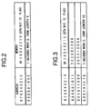
- Figs. 2 and 3 show examples of setting of the memory 10 in Fig. 1.
- Fig. 2 there is illustrated a setting in which "A" as the decoded word a, "4" as the code length b and "1" of the flag c corresponding to the Huffman code data sequence "0101" is set in the address "000001010".
- the pointer p and the flag c (0" are set in the addresses "000001011” and "00001000”
- "C" as the decoded word a, "10” as its code length b and "1” as the flag c corresponding to the Huffman code data sequence "1101000101” is set in the address "00010**10".
- the 9th bit indicates the flag (c).
- the input of the selector 12 is selected to the side of the input A1 by the selector signal e.
- the leading one bit of the 4th bit "0" of the Huffman code "0101" is input to the lowermost address AL of the memory 10.
- the 3rd bit to 1st bit of the Huffman code "101" is input to the intermediate address AHL of the memory 10 via the input A1 of the selector 12.
- the pointer p "00001000” and the flag c "0" are output from the memory 10. Since this memory output is the pointer p, decoding process (tracking) is performed again on the basis of this pointer p and the next 4 bits of the Huffman code.
- the latch circuit 11 latches the pointer to output "00001000".
- the upper 5 bits "00001” is input to an upper address AHH.
- the 6th bit (leading bit) "0" of the Huffman code is input to the lowermost address AL of the memory 10.
- the 5th bit to 3rd bit "001" of the Huffman code is input to the intermediate address AHL of the memory 10 via the input A1 of the selector 12.
- an address "000011000” is input.
- the pointer p "00010000" and the flag c "0" are output from the memory 10. Since this memory output is the pointer p, decoding process (tracking) is performed again on the basis of this pointer p and the next 4 bits of the Huffman code.
- the latch circuit 11 latches the pointer to output "00010000".
- the upper 5 bits "00010” is input to an upper address AHH.
- the 2nd bit (leading bit) "0" of the Huffman code is input to the lowermost address AL of the memory 10.
- 3 bits consisted of the 1st bit “1" of the Huffman code and leading two bits “*" of the next Huffman code are input to the intermediate address AHL of the memory 10 via the input A1 of the selector 12.
- an address "00010**10" is input.
- the decoded word “C”, the code length "10” and the flag c "1" are output from the memory 10.
- the latch circuit 12 is reset. Then, the leading end of the next Huffman code data sequence d arrives.
- Fig. 4 shows an example of setting of an internal memory when the Huffman code is decoded per each 1 bit.
- the decoded word "A" corresponding to the Huffman code "0101" is set in this case.
- the decoding process in the case that the Huffman code is decoded one by one for each bit will be discussed hereinafter. Namely, the input for the selector 12 is selected to the input A0 side by the selector signal e.
- the upper 5 bits "00000” is input to an upper address AHH.
- the lower 3 bits “000” are input to the intermediate address AHL via the input A0 terminal of the selector 12.
- the leading one bit “0" of the Huffman code is input to the lowermost address AL of the memory 10.
- an address "000000000” is input.
- the pointer "00000001” corresponding to the address "000000000” and the flag c "0" indicative of the pointer output are output from the memory 10.
- the latch circuit 11 latches the above-mentioned pointer and outputs "00000001".
- the upper 5 bits "00000” is input to an upper address AHH.
- the lower 3 bits "001" of the output of the latch circuit 11 are input to the intermediate address AHL via the input A0 terminal of the selector 12.
- the 2nd bit "1" from the leading end of the Huffman code is input to the lowermost address AL of the memory 10.
- an address "000000011” is input.
- the pointer "00000010" corresponding to the address "000000011” and the flag c "0" are output from the memory 10.
- the latch circuit 11 latches the above-mentioned pointer and outputs "00000011".
- the upper 5 bits "00000” is input to an upper address AHH.
- the lower 3 bits “011” of the output of the latch circuit 11 are input to the intermediate address AHL via the input A0 terminal of the selector 12.
- the 2nd bit "1" from the leading end of the Huffman code is input to the lowermost address AL of the memory 10.
- an address "000000111” is input.
- the decoded word "A”, the code length "4" and the flag c "1" are output from the memory 10.
- the flag "1 the latch circuit 11 is reset, and then the leading end of the next Huffman code data sequence arrives thereto. Subsequently, the similar decoding processes are repeated.
- the input A1 side of the selector 12 is selected by the selector signal e
- the input A0 side of the selector 12 is selected by the selector signal e. Accordingly, an importance is given for the decoding speed, decoding for every 4 bits is selected in the memory 10. It should be noted, however, that when decoding for every 4 bits is to be performed, the decoding table becomes greater than that of decoding for every 1 bit in the extend of 8 times at the maximum to cause increasing of the cost. Accordingly, when an importance is given for the cost, a decoding tree per 1 bit is set in the memory 10 to perform decoding for every 1 bit.
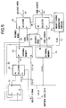
- the second embodiment of the Huffman code decoding circuit is illustrated in Fig. 5.
- the second embodiment of the Huffman code decoding circuit generally comprises a latch circuit 31 with a reset function, a selector 32, an internal memory 33, an external memory 34, a selector 35, a selector 36 and a select signal generating circuit 37.
- the internal memory 33 is a memory provided in the same chip with the Huffman code decoding circuit
- the external memory 34 is a memory provided externally to the Huffman code decoding circuit.
- the internal memory 33 has a construction of 1 kW (word) x 13 bits. This internal memory 33 has addresses of 10 bits. A leading 2 bits of a Huffman code data sequence h of 16 bits are input as the lowermost address AL. On the other hand, 8 bits of the output of the selector 32 is output as 3rd to from 10th bits of the upper address AH.
- the internal memory 33 expresses a decoded word a or pointer p with 8 bits among 13 bits, the code length b and the flag c with remaining 5 bits. From the output QD of the internal memory 33, the decoded word a (or the pointer p) is output. From an output QF, the code length b and flag c are output. This flag c indicates whether the output of the internal memory 33 is the decoded word (whether the output of the internal memory 33 is effective) or not.
- the flag c is set to "1"
- the pointer p (next address of the memory 10) is output from the output QD (during continuation of decoding process)
- the flag c is set to "0".
- the external memory 34 has a construction of 8 kW x 13 bits. This external memory 34 has an address of 13 bits so that lower 13 bits of the 16 bits Huffman code data sequence h is input as the address.
- the external memory expresses the decoded word a with 8 bits in the 13 bits, and the code length b with the remaining 5 bits. From the output QD of the external memory 34, the decoded word a is output and from the output QFR, the code length b is output.
- the latch circuit 31 latches 8 bits of the pointer p output from the internal memory 33 when the flag is "0". On the other hand, when the flag c is "1", the latch circuit 11 is reset to output a data having "0" in all 8 bits.
- the selector 32 selects either input A0 or A1 on the basis of the select signal e to output to the upper address AH.
- the input A0 is selected.
- the input A0 is selected by the select signal e.
- the 8 bits of the output from the latch circuit 11 is input and then output to the upper address AH of the internal memory 33.
- the input A1 is selected by the select signal e.
- 8 bits of the 13th to 6th bits of the Huffman code data sequence h is input and then output to the upper address AH of the internal memory 33.
- the selector 35 selects output from the internal memory 33 or the output from the external memory 34 to output as the decoded word to output.
- the selector 36 selects the output of the internal memory 33 or the output from the external memory 34 to output as the code length to output.
- the select signal generating circuit 37 outputs a select signal for selecting the output of the internal memory 33 to the selectors 35 and 36 when the outputs of the internal memory 33 are effective.
- the decoded word and the code length are set.
- the 5th bit of the 5 bits indicative of the code length in the internal memory 33 serves for setting and resetting the flag c.
- the decoded word and the code length corresponding to higher than and equal to 11th bit to and lower than or equal to 16th bit.
- high speed decoding process can be performed by the internal memory 33 as long as the Huffman code length is less than or equal to 10 bits.
- decoding is performed by tracking the decoding tree of each one bits.
- decoding process is performed by using the internal memory 33 and the external memory 34.
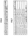
- Fig. 6 shows an example of setting of the internal memory 33 in Fig. 5.
- discussion will be given for the case where the code length of the Huffman code data sequence h is less than or equal to 10 bits and thus permits decoding process only by the internal memory 33.
- the decoded word "D" and the code length "6" corresponding to the Huffman code "010101" are set in the address "****101010” and the 16 bits Huffman code data sequence "010101." is received.
- the A1 side input of the selector 32 is selected by the selector signal e.
- the latch circuit 31 is in the reset state. Therefore, "0" is output for all 8 bits from the latch circuit 31. Although the 8 bits from the latch circuit 31 is input to the A0 input of the selector 32, since the selector 32 is selected to the A1 input side, these 8 bits are ignored.
- the leading two bits (15th bit and 14th bit) "01" of the Huffman code data sequence h is input to the lower address AL of the internal memory 33. Namely, the leading bit (15th bit) becomes the least significant bit.
- the 8 bits from 13th bit to 6th bit of the Huffman code data sequence h are input to the upper address AH of the memory 10 via the input A1 of the selector 12.
- an address "****101010” is input to the internal address 33. It should be noted that "****" is bits of the next Huffman code following to the Huffman code "010101" and can be either "0" or "1".
- Fig. 7 shows another example of setting of the internal memory 33.
- the content of the internal memory 33 illustrated in Fig. 7 is an example for decoding the Huffman code per every 2 bits. It is assumed that the decoded word "B" and the code length "11" corresponding to the Huffman code "11111010001" is set in an address "00000101*1", and 16 bits Huffman code data sequence "11111010001." is received, as shown in Fig. 7. Since decoding process is to be performed for every 2 bits, input of the selector 32 is selected at the input A0 side by the selector signal e.
- this 8 bits is input to the upper address AH of the internal memory 33 via the A0 input of the selector 32.
- next two bits (7th bit and 6th bit) "00" of the Huffman code data sequence h is input to the lower address AL of the internal memory 33. Accordingly, an address "0000010000” is input to the internal address 33.
- the address input for the external memory 34 is input with excluding the leading 3 bits (15th ⁇ 13th bits)
- the decoded word "D” and the code length "6” are set in all of addresses "****101010” (i.e. 8 addresses of 0000101010 ⁇ 01111010101" when the Huffman code is "010101", for example.
- the decoded word "B” and the code length "11” are set in all addresses from "1101000100000” ⁇ "1101000111111” when the Huffman code corresponding to the decoded word "B” is "11111010001", for example.
- the decoded words and the code lengths obtained from the internal memory 33 and the external memory 34 are fed to the selectors 35 and 36.
- the selectors 35 and 36 thus outputs the decoded word "D" and the code length "6".
- the code length "6" is fed to the Huffman code data sequence h for determining the leading end of the next Huffman code data sequence h.
- the leading two bits "11” are input to the lower address AL, and 8 bits from leading 3rd bit to 10th bit (upper 13 bit ⁇ 6 bit) "11101000" are input to the upper address AH via the A1 input of the selector 32. Accordingly, in the internal memory 33, an address "0001011111” is input. However, since the flag c is set at "0", null of the output of the internal memory 33 ia notified to the select signal generating circuit 37.
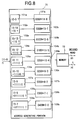
- the third embodiment of the Huffman code decoding circuit comprises an address generating circuit 71 for detecting a predetermined code sequence pattern from the data sequence of the Huffman code and generating an address corresponding to the detected pattern, and a memory 72 for inputting the address output from the address generating circuit and outputting the decoded word and the code length corresponding to the address.
- the address generating circuit 71 includes pattern detecting portions 101a ⁇ 109a and address deriving portions 101b ⁇ 109b.
- This Huffman code decoding circuit uses the fact that number of bits following "0" is less than or equal to 7, when the number of word of the Huffman code is less than or equal to 256, and when "0" is present in the code data sequence.
- the maximum code length L of the Huffman code is 16 bits and the decoded word is 8 bits.
- the pattern detecting portion 101a of the address generating circuit 71 detects whether the leading bit of the Huffman code data sequence d, namely the 15th bit, is "0" or not with respect to the Huffman code data sequence d consisted of 15th to 0th bits with taking 15th bit as the leading bit.
- the address deriving portion 101b adds 7 bits of 14th bit to 8th bit to "0000(H)" to derive the address.
- the pattern detecting portion 102a of the address generating circuit 71 detects whether the 15th bit is "1" and the second leading bit, i.e. 14th bit is "0".
- the address deriving portion 102b adds 7 bits of 13th bit which is the third leading bit, to 7th bit to "0080(H)" to derive the address.
- the pattern detecting portion 103a of the address generating circuit 71 detects whether leading two bits, i.e. the 15th and 14th bits are "1" and the 13th bit is "0". When the pattern detecting portion 103a detects that the 15th and 14th bits are "1” and the 13th bit is "0", the address deriving portion 103b adds 7 bits of 12th bit which is the fourth leading bit, to 6th bit to "0100(H)" to derive the address.
- the pattern detecting portion 104a of the address generating circuit 71 detects whether leading three bits, i.e. the 15th ⁇ 13th bits are "1" and the 12th bit is "0". When the pattern detecting portion 104a detects that the 15th ⁇ 13th bits are "1” and the 12th bit is "0", the address deriving portion 104b adds 7 bits of 11th bit which is the fifth leading bit, to 5th bit to "0180(H)" to derive the address.
- the pattern detecting portion 105a of the address generating circuit 71 detects whether leading four bits, i.e. the 15th ⁇ 12th bits are "1" and the 11th bit is "0". When the pattern detecting portion 105a detects that the 15th ⁇ 12th bits are "1” and the 11th bit is "0", the address deriving portion 105b adds 7 bits of 10th bit which is the sixth leading bit, to 4th bit to "0200(H)" to derive the address.
- the pattern detecting portion 106a of the address generating circuit 71 detects whether leading five bits, i.e. the 15th ⁇ 11th bits are "1" and the 10th bit is "0". When the pattern detecting portion 106a detects that the 15th ⁇ 11th bits are "1” and the 10th bit is "0", the address deriving portion 106b adds 7 bits of 9th bit which is the seventh leading bit, to 3rd bit to "0280(H)" to derive the address.
- the pattern detecting portion 107a of the address generating circuit 71 detects whether leading six bits, i.e. the 15th ⁇ 10th bits are "1" and the 9th bit is "0".
- the address deriving portion 107b adds 7 bits of 9th bit which is the eighth leading bit, to 2nd bit to "0300(H)" to derive the address.
- the pattern detecting portion 108a of the address generating circuit 71 detects whether leading seven bits, i.e. the 15th ⁇ 9th bits are "1" and the 8th bit is "0". When the pattern detecting portion 108a detects that the 15th ⁇ 9th bits are "1” and the 8th bit is "0", the address deriving portion 108b adds 7 bits of 7th bit which is the ninth leading bit, to 1st bit to "0380(H)" to derive the address.
- the pattern detecting portion 109a of the address generating circuit 71 detects whether leading eight bits, i.e. the 15th ⁇ 8th bits are "1" and the 7th bit is "0".
- the address deriving portion 109b adds 8 bits of 7th bit which is the ninth leading bit, to 0th bit to "0400(H)" to derive the address.
- summing operation is performed by replacing the lower 7 or 8 bits of the input Huffman code data to binary numbers as converted from hexa-decimal numbers "0000", “0080”, “0100”, “0180”, “0200”, “0280”, “0300”, “0380” and "0400".
- the Huffman code data sequence d input to the address generating circuit 71 is 16 bits of "0001......".
- the 15th bit as the leading bit is "0”, it is detected by the pattern detecting portion 101a.
- 7 bits of 14th to 8th bits is added to "0000(H)" to derive the address "001****" and output to the memory 72.
- the Huffman code data sequence d input to the address generating circuit 71 is "11111010001..". Since the leading six bits is “111110", "1" in the 15th to 11th bits and "0" in the 10th bit are detected by the pattern detecting portion 106a. Then, in the address deriving portion, 7 bits of 9th ⁇ 3rd bits "10001**" are added to "0280(H)" and then output to the memory 72 as address.
- the decoded word "C” and the code length L “11” are set for the addresses "0000001011000100” ⁇ "0000001011000111", the decoded word “C” and the code length "11” are output from the memory 72.
- the code length "11” the leading end of the Huffman code data sequence h is determined so that 16 bits from the leading end is input to the address generating circuit 71.Subsequently, the similar manner of operations are repeated to perform decoding operation.
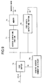
- the fourth embodiment of the Huffman code decoding circuit is constructed by adding a code buffer 73 for temporarily holding the Huffman code data sequence d, a memory 74 in place of the memory 72 and having a capacity of 1280 W x 8 bits, a code length outputting portion 75 and a leading address designating circuit 76 for designating the leading end of the Huffman code data sequence d, to the construction of the third embodiment set forth above.
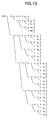
- Fig. 10 shows one example of distribution of the code length of the Huffman code data sequence d.
- the 8 bits decoded words are set.
- the code lengths are set in the code length outputting portion 5 so that the code length L of the decoded word is output in the basis of the code length distribution.
- the Huffman code corresponding to the decoded word "A” is "0001". Accordingly, in the memory 74, the decoded word "A" is set for all addresses "0000000000010000" ⁇ "0000000000011111".
- the code buffer 73 accumulates the data sequence d and feed to the address generating circuit 71 and the code length outputting portion 75.
- the address generating circuit 71 since the leading 15th bit is "0", the pattern detecting portion 101a of the address outputting portion 101 detects this to derive the address by adding 7 bits "001****" of 14th to 8th bits to "0000(H) by the address deriving portion 101b, and to output to the memory 72. Therefore, the decoded word "A” and the code length L "4" corresponding to addresses "0000000000010000” ⁇ "0000000000011111" are output from the memory 72.
- the code length L "4" thus output is fed to the leading address designating circuit 76.
- the leading address designating circuit 76 makes judgement that the leading 4 bits of the Huffman code data sequence d accumulated in the code buffer 73 is the Huffman code corresponding to the decoded word "A" on the basis of the transmitted code length L "4", and then transmit a leading end designating signal H for designating that the leading 5th bit becomes the leading bit of the next Huffman code data sequence d.
- the code buffer 73 accumulates 16 bits from the bit designated by the transmitted leading end designating signal H as new Huffman code data sequence and feeds to the address generating circuit 71 and the code length outputting portion 75. By repeating the foregoing operation, decoding process can be performed.
- the invention should not be specified to the shown embodiment. Namely, in case of the Huffman code consisted of a data sequence of 2 (m+1) (m is integer) bits or mote, a plurality of addresses are generate for a plurality of Huffman codes by detecting the pattern of the data sequence, in which the bits from the leading bit to the nth (n: integer) bit contain logical "1", and the n+1th bit contains logical "0", is detected by the pattern detecting portion, and by adding the data of m bits from n+2th bit to n+2+mth bit to 2 m x (n + 1) when the pattern is detected.
- the number of bits to be added in each address deriving portion is 6 or less, e.g. 5, relative to the 16 bits of the Huffman code input to the address for reducing the memory capacity.
Description
- The present invention relates to a Huffman code decoding circuit for decoding a huffman code. More specifically, the invention relates to a Huffman code decoding circuit to be used for data compression in an image compression processing system or so forth and is capable of realizing improvement for decoding process speed and integration.
- Conventional huffman code decoding circuit employs a memory having an address for a maximum code address or a circuit for tracking a decoding tree for each bit in order to attribute a decoded word corresponding to the Huffman code.
- Fig. 11 is a block diagram showing another conventional Huffman code. As shown in Fig. 11, the decoding circuit performs decoding process by tracking a decoding tree for each bit. The decoding circuit has a
latch 210 and aninternal memory 211. Theinternal memory 211 is of construction of 512 W x 9 bits. In theinternal memory 211, a leading one bit of a Huffman code data sequence is input as a least significant address, and 8 bits of an output of thelatch circuit 210 is also input as upper 8 bits of the address. - On the other hand, the
latch circuit 210 latches a pointer when the pointer is output from theinternal memory 211. Among 9 bits of the output of theinternal memory - In the operation of the decoding circuit set forth above, at first, a memory address is determined based on 1 bit input from the Huffman code data sequence to obtain the output of the
internal memory 211. When the output result is the pointer, theinternal memory 211 is again accessed based on the pointer and the next 1 bit of the Huffman code data sequence. When the output is the decoded word, one cycle of decoding process is finished. - Such circuit to perform decoding by tracking the decoding tree for each bit, memory access for the times corresponding to number of code bits to lower decoding process speed.
- A further example of the Huffman code decoding circuit, in which the decoding process speed is improved, is illustrated in Fig. 12. As shown in Fig. 12, the shown Huffman code decoding circuit has a
memory 219 having address with a length corresponding to the maximum code length. Thismemory 219 has a construction of 64 kW x 13 bits. Namely, the Huffman code data sequence is input to an address input of thememory 219. Then, a decoded word and a code length are obtained as the output of thememory 219 corresponding to the address. Here, assuming that the maximum code length is 16 bits and the decoded word is 8 bits, the 8 bits of the decoded word and 5 bits code length. For instance, the decoded word for "all of addresses "01010 ... 0" ∼ "01011...1" A and the code length "4" are set. Similarly, for each address is set with respect to the Huffman code for each decoded word. - In the Huffman code decoding circuit, at first, 16 bits from the leading bit of the Huffman code data sequence is input to the address in the
memory 219. Assuming that "0101....." is transmitted, "0101 ...", "0101" is input to the 4 upper bits of thememory 219, and a Huffman code is input to the 12 lower bits. As set forth above, since the decoded word "A" and the code length "4" are set are set in respective addresses "01010 ... 0" ∼ "01011...1", the decoded word "A" and the code length "4" can be derived. With the code length "4", the leading bit of the Huffman code and 16 bits is determined and then the 16 bits are input to the address of thememory 219. In the similar manner, decoding process is repeated. - In such decoding circuit, the process speed may be improved. However, assuming that the maximum code length is 16 bits, it requires the memory size to be 65536 W. Therefore, when it is caused to causes increasing of the area and cost.
- On the other hand, as a still further example of the conventional Huffman code decoding circuit, in which a method for providing a plurality of memory for accessing simultaneously and selecting the decoded word is employed. The construction of this type of the Huffman code decoding circuit is illustrated in Fig. 13. The shown decoding circuit includes a
memory 301 ∼ 309 taking the leading 15 bits so that 14th ∼ 8th bits, 13th ∼ 7th bits, 12th ∼ 6th bits, 11th ∼ 5th, 10th ∼ 4th bits, 9th ∼ 3rd bits, 8th ∼ 2nd bits, 7th ∼ 1st bits and 7th ∼ 0th being taken as address inputs relative to the 16 bits of 15th ∼ 0th bits. aselector 401, and a select signal generatingcircuit 402 for controlling theselector 401. - This circuit utilizes the fact that when number of word of the Huffman code is less than or equal to 256 words, and when "0" is present in the data sequence of the code, number of bits following the relevant bit is less than or equal to 7 bits.
- At first, respective 8 bits decoded words and 4 bits code length are set in
memories 301 ∼ 309. Thememory 301 is set the decoded word and the code length in the case of the decoded word representative of the Huffman code having "0" in the leading bit. For instance, if the Huffman code corresponding to the decoded word "A" is "0001", the decoded word "A" and the code length "4" are set for all of addresses "00100000" ∼ "00111111" of thememory 301. - Similarly, the
memory 302 is set the decoded word and the code length in the case of the decoded word representative of the Huffman code having "0" in the second leading bit. For instance, if the Huffman code corresponding to the decoded word "B" is "10011", the decoded word "B" and the code length "5" are set for all of addresses "01100000" ∼ "01111111" of thememory 302. Subsequently, in the similar manner, when a pattern of the data sequence is a sequence, in which "0" is added for the trailing end of a sequence of "1" containing i (integer) -1 in number of "1", the decoded word and the code length are set in the first memory. On the other hand, all of the leading 8 bits are "1", i.e. "11111111" , the decoded word and the code length are set for thememory 309. - The operation will be discussed hereinafter. Among 16 bits Huffman code data sequence, 7 bits from the 14th bit as the second leading bit to the 8th bits as the second leading bits are stored in the
first memory 301, the 13th bits ∼ 6th bits as the leading third bits are stored in thememory 302. Subsequently, in the same manner, up to theseventh memory memory 309. At the same time, 16 bits are supplied to a selectsignal generating portion 402. - Here, consideration is given for the case where the Huffman code data sequence "0001....." is input. Then, "001" is input to the upper 3 bits of the address of the
memory 301. Since thememory 301 is set the decoded word "A" and the code length "4" for all addresses of "00100000" ∼ "00111111", the decoded word "A" and the code length "4" are output in response to the above-mentioned Huffman code. With respect toother memories 302 ∼ 309, the decoded words and the code length corresponding to the above-mentioned address input are output. The outputs of thesememories 301 ∼ 309 are input toinputs 0 ∼ 8 of theselector 401. - The select
signal generating portion 402 feeds a select signal for selecting the output of thememory 301 to theselector 401 when the leading bit, i.e. 15th bit of the data sequence is "0". On the other hand, when the pattern of the data sequence is that "0" is added the trailing end of i-1 of series of "1", the select signal generating portion 403 feeds the select signal to the selector for selecting the first memory. For instance, when the above-mentioned pattern is "10", since i = 2, the signal selecting the 2nd memory (i = 2) 302 is fed. On the other hand, in case of the pattern having "1" in all bits, the signal selecting the 9th memory (i = 9) 309 us fed to the selector. - The code length "4" of the
1st memory 301 output from theselector 401 us fed to the Huffman code data sequence. Thus, the leading end of the next Huffman code data sequence is determined. Subsequently, the decoding process is performed in the similar manner. - In case of the above-mentioned example, 128 words x 12 bits x 8 (
memories 301 ∼ 308) + 256 words x 12 bits x 1 (memory 309) =1280 words x 12 bits. In the decoding circuit constructed as set forth above, a plurality of memories are required to require greater chip area that a single memory of the same capacity, and expensive. - US-A-4 899 149 discloses a method and an apparatus for Huffman or variable-length codes. Variable-length code-words are divided into two parts, a variable-length prefix part and the remainder of the code-word which is of fixed-length or approximately so. The variable-length part consists of a series of 1's terminated by a single 0 bit, the number of 1's preceding the first 0 bit indicates the prefix of a particular code-word. The code-words are arranged so that the ones with the same prefix have the same length, or as close as possible. With this codification, decoding the variable-length code-words is accomplished in two simple steps. In the first step the decoder determines the position of the first 0 bit in the present code-word, using this information to specify a section of the main memory. The second step is to index into that memory section using the remaining part of that code-word, and this retrieve the fixed length representation.
- Therefore, it is a first object of the present invention to provide a Huffman code decoding circuit eliminating the defects in the prior art, achieving higher decoding process speed, reducing required memory capacity and facilitating integration.
- A second object of the present invention is to provide a Huffman code decoding circuit which permits selection of various decoding systems in consideration of speeding of the decoding process and downsizing of a memory.
- A third object of the invention is to provide a Huffman code decoding circuit which can reduce a chip area in integration and lower a cost.
- The present invention is defined in
independent claims - It is to be understood that only the third and fourth embodiments described hereinafter form embodiments of the invention as claimed, while the first and second embodiments are for illustrative purposes only and do not form embodiments of the invention.
- The present invention will be understood more fully from the detailed description given herebelow and from the accompanying drawings of the preferred embodiment of the invention.
- In the drawings:
- Fig. 1 is a block diagram of the first embodiment of a Huffman code decoding circuit,
- Fig. 2 is an explanatory illustration showing an example of setting of a memory in the first embodiment;
- Fig. 3 is an explanatory illustration showing an example of setting of a memory in the first embodiment;
- Fig. 4 is an explanatory illustration showing an example of setting of a memory in the first embodiment;
- Fig. 5 is a block diagram of the second embodiment of a Huffman code decoding circuit;
- Fig. 6 is an explanatory illustration showing an example of setting of an internal memory in the second embodiment;
- Fig. 7 is an explanatory illustration showing another example of setting of an internal memory in the second embodiment;
- Fig. 8 is a block diagram of the third embodiment of a Huffman code decoding circuit according to the present invention;
- Fig. 9 is a block diagram of the fourth embodiment of a Huffman code decoding circuit according to the present invention;
- Fig. 10 is an illustration showing one example of distribution of code lengths of Huffman code;
- Fig. 11 is a block diagram of the first example of the conventional Huffman code decoding circuit;
- Fig. 12 is a block diagram of the second example of the conventional Huffman code decoding circuit; and
- Fig. 13 is a block diagram of the third example of the conventional Huffman code decoding circuit.
-
- The preferred embodiments of the present invention will be discussed with reference to Figs. 1 ∼ 7. Initially, discussion will be given for the first embodiment of a Huffman code decoding circuit with reference to Fig. 1. The first embodiment of the Huffman code decoding circuit, illustrated in Fig. 1, generally comprises a
memory 10, alatch circuit 11 with a reset function and aselector 12. - The
memory 10 has a construction of 512 W (word) x 9 bits. Thismemory 10 has addresses of 9 bits. A leading 1 bit of a Huffman code data sequence d is input as the least significant bit (lowermost address AL). On the other hand, 3 bits of the output of theselector 12 is output as 4 bits from 2nd bit of an address (intermediate address AHL). Among 8 bits as the output of thelatch circuit 11, upper 5 bits are input as upper 5 bits (upper address AHH). - The
memory 10 expresses a decoded word a and a code length b or pointer p with 8 bits in 9 bits, and remaining 1 bit expresses a flag c. - From the output QD of the memory, the decoded word a (or the pointer p) and the code length b are output. From an output QF, the flag c is output. This flag c is indicative of decoding condition of the Huffman code. For example, when the decoded word a is derived from the output QD, the flag c is set to "1", and when the pointer p (next address of the memory 10) (during continuation of decoding process), the flag c is set to "0".
- The
latch circuit 11 with the reset function, latches 8 bits of the pointer p output from thememory 10 when the flag is "0". On the other hand, when the flag c is "1", thelatch circuit 11 is reset to output a data having "0" in all 8 bits. - On the other hand, the
selector 12 selects either input A0 or A1 on the basis of the select signal e to output to the intermediate address AHL. When decoding of the Huffman code data sequence d is to be performed per each bit, the input A0 is selected. In this case, the input A0 is selected by the select signal e. In this case, for the input A0 of the selector, the lower 3 bits among 8 bits of the output from thelatch circuit 11 to the intermediate address AHL. On the other hand, when decoding of the Huffman code data sequence is to be performed per 4 bits of the Huffman code data, the input A1 is selected by the select signal e. In this case, to the input A1, the upper 3 bits of the Huffman code data sequence d is input to the intermediate address AHL of thememory 10. - Figs. 2 and 3 show examples of setting of the
memory 10 in Fig. 1. In Fig. 2, there is illustrated a setting in which "A" as the decoded word a, "4" as the code length b and "1" of the flag c corresponding to the Huffman code data sequence "0101" is set in the address "000001010". On the other hand, in Fig. 3, the pointer p and the flag c ("0") are set in the addresses "000001011" and "00001000", and "C" as the decoded word a, "10" as its code length b and "1" as the flag c corresponding to the Huffman code data sequence "1101000101" is set in the address "00010**10". It should be noted that, in thememory 1, the 9th bit indicates the flag (c). - Discussion for decoding process of the Huffman code data sequence per every 4 bits hereinafter. Namely, the input of the
selector 12 is selected to the side of the input A1 by the selector signal e. - At first, it is assumed that the former decoding of the Huffman code d is completed, the
latch circuit 11 is reset by the flag c = "1", and the Huffman code "0101" corresponding to the decoded word "A" of Fig. 2 is provided as the next Huffman code d. - From the
latch circuit 11, "0" is output for all 8 bits in response to resetting. Among this 8 bits, the upper 5 bits "00000" is input to an upper address AHH. On the other hand, the lower 3 bits are input to an input A0 terminal of theselector 12. In this case, however, since the input A1 side is selected by the select signal e, the lower 3 bits of thelatch circuit 11 is ignored. - Next, the leading one bit of the 4th bit "0" of the Huffman code "0101" is input to the lowermost address AL of the
memory 10. The 3rd bit to 1st bit of the Huffman code "101" is input to the intermediate address AHL of thememory 10 via the input A1 of theselector 12. - As a result, to the memory, an address "000001010" is input with the upper address AHH "00000", the intermediate address "101" and the lowermost address "0". Then, the decoded word "A", the code length "4" and the flag c "1" are output from the
memory 10. Subsequently, the leading end of the next Huffman code data sequence arrives. - It is further assumed that, as the next Huffman code data sequence d, the Huffman code "1101000101" corresponding to the decoded word C illustrated in Fig. 3 is transmitted. From the
latch circuit 11, "0" is output for all 8 bits in response to resetting. Among this 8 bits, the upper 5 bits "00000" is input to an upper address AHH. The 10th bit (leading bit) "1" of the Huffman code is input to the lowermost address AL of thememory 10. The 9th bit to 7th bit "101" of the Huffman code is input to the intermediate address AHL of thememory 10 via the input A1 of theselector 12. As a result, to the memory, an address "000001011" is input. Then, the pointer p "00001000" and the flag c "0" are output from thememory 10. Since this memory output is the pointer p, decoding process (tracking) is performed again on the basis of this pointer p and the next 4 bits of the Huffman code. - Next, the
latch circuit 11 latches the pointer to output "00001000". Among this 10 bits, the upper 5 bits "00001" is input to an upper address AHH. The 6th bit (leading bit) "0" of the Huffman code is input to the lowermost address AL of thememory 10. The 5th bit to 3rd bit "001" of the Huffman code is input to the intermediate address AHL of thememory 10 via the input A1 of theselector 12. As a result, to the memory, an address "000011000" is input. Then, the pointer p "00010000" and the flag c "0" are output from thememory 10. Since this memory output is the pointer p, decoding process (tracking) is performed again on the basis of this pointer p and the next 4 bits of the Huffman code. - In the next process cycle, the
latch circuit 11 latches the pointer to output "00010000". Among this 10 bits, the upper 5 bits "00010" is input to an upper address AHH. The 2nd bit (leading bit) "0" of the Huffman code is input to the lowermost address AL of thememory 10. 3 bits consisted of the 1st bit "1" of the Huffman code and leading two bits "*" of the next Huffman code are input to the intermediate address AHL of thememory 10 via the input A1 of theselector 12. As a result, to the memory, an address "00010**10" is input. Then, the decoded word "C", the code length "10" and the flag c "1" are output from thememory 10. - The foregoing two bits "**" are leading 2 bits of the next Huffman code, and thus can be either "0" or "1". Namely, in the
memory 10, the decoded word "C", the code length "10" and the flag c "1" indicative of the decoded word output are set in all of the addresses "000100010", "000100110", "000101010" and "000101110". - By the flag c "1", the
latch circuit 12 is reset. Then, the leading end of the next Huffman code data sequence d arrives. - Fig. 4 shows an example of setting of an internal memory when the Huffman code is decoded per each 1 bit. As shown in Fig. 4, , the decoded word "A" corresponding to the Huffman code "0101" is set in this case. The decoding process in the case that the Huffman code is decoded one by one for each bit will be discussed hereinafter. Namely, the input for the
selector 12 is selected to the input A0 side by the selector signal e. - Initially, the former Huffman code decoding cycle is completed and then the
latch circuit 11 is reset by the flag c "1". It is assumed that the Huffman code "0101" corresponding to the decoded word "A" arrives. - 1 bit from the leading end of the Huffman code data sequence is fed to the
memory 10. Then, thelatch circuit 11 is reset to output "0" for all 8 bits. - Among this 8 bits as the output of the
latch circuit 11, the upper 5 bits "00000" is input to an upper address AHH. On the other hand, the lower 3 bits "000" are input to the intermediate address AHL via the input A0 terminal of theselector 12. The leading one bit "0" of the Huffman code is input to the lowermost address AL of thememory 10. As a result, to the memory, an address "000000000" is input. Then, the pointer "00000001" corresponding to the address "000000000" and the flag c "0" indicative of the pointer output are output from thememory 10. - Next, the
latch circuit 11 latches the above-mentioned pointer and outputs "00000001". Among this 8 bits as the output of thelatch circuit 11, the upper 5 bits "00000" is input to an upper address AHH. On the other hand, the lower 3 bits "001" of the output of thelatch circuit 11 are input to the intermediate address AHL via the input A0 terminal of theselector 12. The 2nd bit "1" from the leading end of the Huffman code is input to the lowermost address AL of thememory 10. As a result, to the memory, an address "000000011" is input. Then, the pointer "00000010" corresponding to the address "000000011" and the flag c "0" are output from thememory 10. - Next, the
latch circuit 11 latches the above-mentioned pointer and outputs "00000011". Among the output of thelatch circuit 11, the upper 5 bits "00000" is input to an upper address AHH. On the other hand, the lower 3 bits "011" of the output of thelatch circuit 11 are input to the intermediate address AHL via the input A0 terminal of theselector 12. The 2nd bit "1" from the leading end of the Huffman code is input to the lowermost address AL of thememory 10. As a result, to the memory, an address "000000111" is input. Then, the decoded word "A", the code length "4" and the flag c "1" are output from thememory 10. By the flag "1", thelatch circuit 11 is reset, and then the leading end of the next Huffman code data sequence arrives thereto. Subsequently, the similar decoding processes are repeated. - As set forth above, in the first embodiment, when decoding is to be performed for every 4 bits, the input A1 side of the
selector 12 is selected by the selector signal e, and when decoding is to be performed for every 1 bit, the input A0 side of theselector 12 is selected by the selector signal e. Accordingly, an importance is given for the decoding speed, decoding for every 4 bits is selected in thememory 10. It should be noted, however, that when decoding for every 4 bits is to be performed, the decoding table becomes greater than that of decoding for every 1 bit in the extend of 8 times at the maximum to cause increasing of the cost. Accordingly, when an importance is given for the cost, a decoding tree per 1 bit is set in thememory 10 to perform decoding for every 1 bit. - The second embodiment of the Huffman code decoding circuit according to the present invention is illustrated in Fig. 5. The second embodiment of the Huffman code decoding circuit generally comprises a
latch circuit 31 with a reset function, aselector 32, aninternal memory 33, anexternal memory 34, aselector 35, aselector 36 and a selectsignal generating circuit 37. Here, theinternal memory 33 is a memory provided in the same chip with the Huffman code decoding circuit, and theexternal memory 34 is a memory provided externally to the Huffman code decoding circuit. - The
internal memory 33 has a construction of 1 kW (word) x 13 bits. Thisinternal memory 33 has addresses of 10 bits. A leading 2 bits of a Huffman code data sequence h of 16 bits are input as the lowermost address AL. On the other hand, 8 bits of the output of theselector 32 is output as 3rd to from 10th bits of the upper address AH. - The
internal memory 33 expresses a decoded word a or pointer p with 8 bits among 13 bits, the code length b and the flag c with remaining 5 bits. From the output QD of theinternal memory 33, the decoded word a (or the pointer p) is output. From an output QF, the code length b and flag c are output. This flag c indicates whether the output of theinternal memory 33 is the decoded word (whether the output of theinternal memory 33 is effective) or not. For instance, when the decoded word a is output from the output QD, the flag c is set to "1", and when the pointer p (next address of the memory 10) is output from the output QD (during continuation of decoding process) , the flag c is set to "0". - The
external memory 34 has a construction of 8 kW x 13 bits. Thisexternal memory 34 has an address of 13 bits so that lower 13 bits of the 16 bits Huffman code data sequence h is input as the address. The external memory expresses the decoded word a with 8 bits in the 13 bits, and the code length b with the remaining 5 bits. From the output QD of theexternal memory 34, the decoded word a is output and from the output QFR, the code length b is output. - The
latch circuit 31 with the reset function, latches 8 bits of the pointer p output from theinternal memory 33 when the flag is "0". On the other hand, when the flag c is "1", thelatch circuit 11 is reset to output a data having "0" in all 8 bits. - On the other hand, the
selector 32 selects either input A0 or A1 on the basis of the select signal e to output to the upper address AH. When decoding of the Huffman code data sequence h is to be performed per every 2 bit, the input A0 is selected. In this case, the input A0 is selected by the select signal e. In this case, for the input A0 of the selector, the 8 bits of the output from thelatch circuit 11 is input and then output to the upper address AH of theinternal memory 33. - On the other hand, when decoding of the Huffman code data sequence is to be performed per number of bits other than 2 bits (e.g. per every 16 bits) of the Huffman code data, the input A1 is selected by the select signal e. In this case, to the input A1, 8 bits of the 13th to 6th bits of the Huffman code data sequence h is input and then output to the upper address AH of the
internal memory 33. - The
selector 35 selects output from theinternal memory 33 or the output from theexternal memory 34 to output as the decoded word to output. Theselector 36 selects the output of theinternal memory 33 or the output from theexternal memory 34 to output as the code length to output. - The select
signal generating circuit 37 outputs a select signal for selecting the output of theinternal memory 33 to theselectors internal memory 33 are effective. - Here, in the
internal memory 33 and theexternal memory internal memory 33 serves for setting and resetting the flag c. In theexternal memory 34, the decoded word and the code length corresponding to higher than and equal to 11th bit to and lower than or equal to 16th bit. - With the Huffman code decoding circuit constructed as set forth above, high speed decoding process can be performed by the
internal memory 33 as long as the Huffman code length is less than or equal to 10 bits. When the decoding process speed is not significantly important, decoding is performed by tracking the decoding tree of each one bits. On the other hand, when high speed decoding process is desired irrespective of the cost, decoding process is performed by using theinternal memory 33 and theexternal memory 34. - Fig. 6 shows an example of setting of the
internal memory 33 in Fig. 5. With reference to Fig. 6, discussion will be given for the case where the code length of the Huffman code data sequence h is less than or equal to 10 bits and thus permits decoding process only by theinternal memory 33. - Here, it is assumed that, as shown in Fig. 6, the decoded word "D" and the code length "6" corresponding to the Huffman code "010101" are set in the address "****101010" and the 16 bits Huffman code data sequence "010101...." is received. In addition, in the shown example is directed to the decoding process for performing decoding process for the Huffman code data sequence h per every 16 bits. Therefore, the A1 side input of the
selector 32 is selected by the selector signal e. - At this time, the
latch circuit 31 is in the reset state. Therefore, "0" is output for all 8 bits from thelatch circuit 31. Although the 8 bits from thelatch circuit 31 is input to the A0 input of theselector 32, since theselector 32 is selected to the A1 input side, these 8 bits are ignored. - Next, the leading two bits (15th bit and 14th bit) "01" of the Huffman code data sequence h is input to the lower address AL of the
internal memory 33. Namely, the leading bit (15th bit) becomes the least significant bit. The 8 bits from 13th bit to 6th bit of the Huffman code data sequence h are input to the upper address AH of thememory 10 via the input A1 of theselector 12. As a result, an address "****101010" is input to theinternal address 33. It should be noted that "****" is bits of the next Huffman code following to the Huffman code "010101" and can be either "0" or "1". - Then, the decoded word "D", the code length "6" and the flag c "1" corresponding to the address "****101010" are output from the
internal memory 33. These data are fed to theselectors internal memory 33 is notified to the selectsignal generating circuit 37. Then, from the selectsignal generating circuit 37, the select signal selecting the input A0 is fed to theselectors selectors internal memory 33 are output. Among these, on the basis of the code length output from theselector 36, the leading end of the next Huffman code data sequence h is determined. - Fig. 7 shows another example of setting of the
internal memory 33. The content of theinternal memory 33 illustrated in Fig. 7 is an example for decoding the Huffman code per every 2 bits. It is assumed that the decoded word "B" and the code length "11" corresponding to the Huffman code "11111010001" is set in an address "00000101*1", and 16 bits Huffman code data sequence "11111010001...." is received, as shown in Fig. 7. Since decoding process is to be performed for every 2 bits, input of theselector 32 is selected at the input A0 side by the selector signal e. - At this time, the
latch circuit 31 is in the reset state. Therefore, "0" is output for all 8 bits from thelatch circuit 31. This 8 bits from thelatch circuit 31 is input to the upper address AH of theinternal memory 33 via the A0 input of theselector 32. On the other hand, to the A1 input of theselector internal memory 33 with setting the leading bit (15th bit) at the least significant bit. Accordingly, an address "0000000011" is input to theinternal address 33. Then, from theinternal memory 33, the corresponding pointer "00000001" and the flag c = "0" are output. - This 8 bits of pointer "00000001" is latched by the
latch circuit 31 and output therefrom. Then, this 8 bits is input to the upper address AH of theinternal memory 33 via the A0 input of theselector 32. Next, subsequent two bits (13th bit and 12th bit) "11" of the Huffman code data sequence h is input to the lower address AL of theinternal memory 33. Accordingly, an address "0000000111" is input to theinternal address 33. Then, from theinternal memory 33, the corresponding pointer "00000010" and the flag c = "0" are output. - This 8 bits of pointer "00000010" is latched by the
latch circuit 31 and output therefrom. Then, this 8 bits is input to the upper address AH of theinternal memory 33 via the A0 input of theselector 32. Subsequently, next two bits (11th bit and 10th bit) "10" of the Huffman code data sequence h is input to the lower address AL of theinternal memory 33. Accordingly, an address "0000001001" is input to theinternal address 33. Then, from theinternal memory 33, the corresponding pointer "00000011" and the flag c = "0" are output. - This 8 bits of pointer "00000011" is latched by the
latch circuit 31 and output therefrom. Then, this 8 bits is input to the upper address AH of theinternal memory 33 via the A0 input of theselector 32. Subsequently, next two bits (9th bit and 8th bit) "10" of the Huffman code data sequence h is input to the lower address AL of theinternal memory 33. Accordingly, an address "0000001101" is input to theinternal address 33. Then, from theinternal memory 33, the corresponding pointer "00000100" and the flag c = "0" are output. This 8 bits of pointer "00000100" is latched by thelatch circuit 31 and output therefrom. Then, this 8 bits is input to the upper address AH of theinternal memory 33 via the A0 input of theselector 32. Subsequently, next two bits (7th bit and 6th bit) "00" of the Huffman code data sequence h is input to the lower address AL of theinternal memory 33. Accordingly, an address "0000010000" is input to theinternal address 33. Then, from theinternal memory 33, the corresponding pointer "00000101" and the flag c = "0" are output. - This 8 bits of pointer "00000101" is latched by the
latch circuit 31 and output therefrom. Then, this 8 bits is input to the upper address AH of theinternal memory 33 via the A0 input of theselector 32. Subsequently, next two bits (5th bit and 4th bit) "1*" of the Huffman code data sequence h is input to the lower address AL of theinternal memory 33. "*" is the leading bit of the Huffman code following the Huffman code "11111010001" and can be either "0" or "1". - By this, an address "00000101*1" is input to the
internal address 33. Then, from theinternal memory 33, the decoded word "B" corresponding "00000101*1" and the flag c = "1" are output. These data are fed to theselectors internal memory 33 is notified to the selectsignal generating circuit 37. Therefore, the selectsignal generating circuit 37 outputs the select signal for selecting the A0 input to theselectors selectors internal memory 33 are output. Among these, on the basis of the code length output from theselector 36, the leading end of the next transmitted Huffman code data sequence h is determined. - Next, discussion will be given for the case where decoding process is performed by using both of the
internal memory 33 and theexternal memory 34. - Here, in the
internal memory 33, the decoded words and the code lengths expressed by less than or equal to 10 bits of the 16 bits Huffman code data sequence h. Also, the flag c of theinternal memory 33 is set at the 5th bit of the code length. In theexternal memory 34, the decoded words and the code length correspond to the Huffman code of more than or equal to 11 bits to less than or equal to 16 are set. - It should be appreciated that when the Huffman code is assigned in an order of the code length, the leading 3 bits of the Huffman codes having bits more than or equal to 11 bits always become "111". Therefore, the address input for the
external memory 34 is input with excluding the leading 3 bits (15th ∼ 13th bits) - On the other hand, in the
internal memory 33, the decoded word "D" and the code length "6" are set in all of addresses "****101010" (i.e. 8 addresses of 0000101010 ∼ 01111010101" when the Huffman code is "010101", for example. On the other hand, in theexternal memory 34, the decoded word "B" and the code length "11" are set in all addresses from "1101000100000" ∼ "1101000111111" when the Huffman code corresponding to the decoded word "B" is "11111010001", for example. - Here, consideration is given for the case where the 16 bits Huffman code data sequence "010101....." is transmitted. The leading two bits (15th and 14th bits of the Huffman code data sequence) "01" are input to the lower address AL of the
internal memory 33. On the other hand, 8 bits consisted of 13th to 10th bits of the Huffman code data sequence (i.e. the 3rd to 6th bits from the leading end of the Huffman code) "0101" and leading 4 bits of the next Huffman code "****" are input to the upper address AH of theinternal memory 33 via the A1 input of theselector 32. When both of theinternal memory 33 and theexternal memory 34 are used, theselector 32 is selected at the A1 input side by the select signal e. - Accordingly, in the
internal memory 33, the address "****101010" is input. Then, the decoded word "D", the code length "6", and the flag c = "1" corresponding to the address are output. By the flag c = "1", the selector signal e indicative of the effectiveness of theinternal memory 33 is output from the selectsignal generating circuit 37. On the other hand, theexternal memory 34 outputs the decoded word and the code length corresponding to 13 bits address input. - The decoded words and the code lengths obtained from the
internal memory 33 and theexternal memory 34 are fed to theselectors signal generating circuit 37 feeds the select signal e for selecting the output of theinternal memory 33 to theselectors selectors - Next, consideration is given for the case where the Huffman code data sequence "1111010001.....". In the
internal memory 33, the leading two bits "11" are input to the lower address AL, and 8 bits from leading 3rd bit to 10th bit (upper 13 bit ∼ 6 bit) "11101000" are input to the upper address AH via the A1 input of theselector 32. Accordingly, in theinternal memory 33, an address "0001011111" is input. However, since the flag c is set at "0", null of the output of theinternal memory 33 ia notified to the selectsignal generating circuit 37. - On the other hand, in the
external memory 34, leading 4th to 16 bits (upper 12th bit to 0th bit) "*****10001011" are input as an address. Then, the decoded word "B" and the code length "11" corresponding to "*****10001011" are output from theexternal memory 34. In this case, the select signal e for making the output of theinternal memory 33 null and for making the output of theexternal memory 34 effective, to theselectors selectors selectors external memory 34 are output. The code length "11" is fed to the Huffman code data sequence h to determine the leading end of the next Huffman code data sequence h. - The third embodiment of the Huffman code decoding circuit according to the present invention will be discussed with reference to Fig. 8.
- As shown in Fig. 8, the third embodiment of the Huffman code decoding circuit comprises an
address generating circuit 71 for detecting a predetermined code sequence pattern from the data sequence of the Huffman code and generating an address corresponding to the detected pattern, and amemory 72 for inputting the address output from the address generating circuit and outputting the decoded word and the code length corresponding to the address. - On the other hand, the
address generating circuit 71 includespattern detecting portions 101a ∼ 109a and address derivingportions 101b ∼ 109b. - This Huffman code decoding circuit uses the fact that number of bits following "0" is less than or equal to 7, when the number of word of the Huffman code is less than or equal to 256, and when "0" is present in the code data sequence.
- Here, it is assumed that the maximum code length L of the Huffman code is 16 bits and the decoded word is 8 bits. The
pattern detecting portion 101a of theaddress generating circuit 71 detects whether the leading bit of the Huffman code data sequence d, namely the 15th bit, is "0" or not with respect to the Huffman code data sequence d consisted of 15th to 0th bits with taking 15th bit as the leading bit. When thepattern detecting portion 101a detects "0" at the 16th bit, theaddress deriving portion 101b adds 7 bits of 14th bit to 8th bit to "0000(H)" to derive the address. - The
pattern detecting portion 102a of theaddress generating circuit 71 detects whether the 15th bit is "1" and the second leading bit, i.e. 14th bit is "0". When thepattern detecting portion 102a detects that the 15th bit is "1" and the 14th bit is "0", theaddress deriving portion 102b adds 7 bits of 13th bit which is the third leading bit, to 7th bit to "0080(H)" to derive the address. - The
pattern detecting portion 103a of theaddress generating circuit 71 detects whether leading two bits, i.e. the 15th and 14th bits are "1" and the 13th bit is "0". When thepattern detecting portion 103a detects that the 15th and 14th bits are "1" and the 13th bit is "0", theaddress deriving portion 103b adds 7 bits of 12th bit which is the fourth leading bit, to 6th bit to "0100(H)" to derive the address. - The
pattern detecting portion 104a of theaddress generating circuit 71 detects whether leading three bits, i.e. the 15th ∼ 13th bits are "1" and the 12th bit is "0". When thepattern detecting portion 104a detects that the 15th ∼ 13th bits are "1" and the 12th bit is "0", theaddress deriving portion 104b adds 7 bits of 11th bit which is the fifth leading bit, to 5th bit to "0180(H)" to derive the address. - The
pattern detecting portion 105a of theaddress generating circuit 71 detects whether leading four bits, i.e. the 15th ∼ 12th bits are "1" and the 11th bit is "0". When thepattern detecting portion 105a detects that the 15th ∼ 12th bits are "1" and the 11th bit is "0", theaddress deriving portion 105b adds 7 bits of 10th bit which is the sixth leading bit, to 4th bit to "0200(H)" to derive the address. - The
pattern detecting portion 106a of theaddress generating circuit 71 detects whether leading five bits, i.e. the 15th ∼ 11th bits are "1" and the 10th bit is "0". When thepattern detecting portion 106a detects that the 15th ∼ 11th bits are "1" and the 10th bit is "0", theaddress deriving portion 106b adds 7 bits of 9th bit which is the seventh leading bit, to 3rd bit to "0280(H)" to derive the address. - The
pattern detecting portion 107a of theaddress generating circuit 71 detects whether leading six bits, i.e. the 15th ∼ 10th bits are "1" and the 9th bit is "0". When thepattern detecting portion 107a detects that the 15th ∼ 10th bits are "1" and the 9th bit is "0", theaddress deriving portion 107b adds 7 bits of 9th bit which is the eighth leading bit, to 2nd bit to "0300(H)" to derive the address. - The
pattern detecting portion 108a of theaddress generating circuit 71 detects whether leading seven bits, i.e. the 15th ∼ 9th bits are "1" and the 8th bit is "0". When thepattern detecting portion 108a detects that the 15th ∼ 9th bits are "1" and the 8th bit is "0", theaddress deriving portion 108b adds 7 bits of 7th bit which is the ninth leading bit, to 1st bit to "0380(H)" to derive the address. - The
pattern detecting portion 109a of theaddress generating circuit 71 detects whether leading eight bits, i.e. the 15th ∼ 8th bits are "1" and the 7th bit is "0". When thepattern detecting portion 109a detects that the 15th ∼ 8th bits are "1" and the 7th bit is "0", theaddress deriving portion 109b adds 8 bits of 7th bit which is the ninth leading bit, to 0th bit to "0400(H)" to derive the address. - Here, in either case in adding 7 bits and 8 bits, summing operation is performed by replacing the lower 7 or 8 bits of the input Huffman code data to binary numbers as converted from hexa-decimal numbers "0000", "0080", "0100", "0180", "0200", "0280", "0300", "0380" and "0400".
- In the
memory - Initially, it is assumed that the Huffman code data sequence d input to the
address generating circuit 71 is 16 bits of "0001......". The 15th bit as the leading bit is "0", it is detected by thepattern detecting portion 101a. Then, in theaddress deriving portion memory 72. - As set forth above, all of the address of the
memory 72 "0000000000010000" - "0000000000011111" are set with the decoded word "A" and the code length "4". The decoded word "A" and the code length "4" are output from thememory 72 corresponding to the above-mentioned address. By the code length "4", the leading end of the Huffman code data sequence h is determined so that 16 bits from the leading end is input to theaddress generating circuit 71. - Next, it is assumed that the Huffman code data sequence d input to the
address generating circuit 71 is "11111010001.....". Since the leading six bits is "111110", "1" in the 15th to 11th bits and "0" in the 10th bit are detected by thepattern detecting portion 106a. Then, in the address deriving portion, 7 bits of 9th ∼ 3rd bits "10001**" are added to "0280(H)" and then output to thememory 72 as address. - As set forth above, the decoded word "C" and the code length L "11" are set for the addresses "0000001011000100" ∼ "0000001011000111", the decoded word "C" and the code length "11" are output from the
memory 72. By the code length "11", the leading end of the Huffman code data sequence h is determined so that 16 bits from the leading end is input to the address generating circuit 71.Subsequently, the similar manner of operations are repeated to perform decoding operation. - Next, the fourth embodiment of the Huffman code decoding circuit according to the invention will be discussed with reference to Fig. 9.
- The fourth embodiment of the Huffman code decoding circuit is constructed by adding a
code buffer 73 for temporarily holding the Huffman code data sequence d, amemory 74 in place of thememory 72 and having a capacity of 1280 W x 8 bits, a codelength outputting portion 75 and a leadingaddress designating circuit 76 for designating the leading end of the Huffman code data sequence d, to the construction of the third embodiment set forth above. - On the other hand, Fig. 10 shows one example of distribution of the code length of the Huffman code data sequence d.
- In the
memory 74, the 8 bits decoded words are set. On the other hand, the code lengths are set in the codelength outputting portion 5 so that the code length L of the decoded word is output in the basis of the code length distribution. Similarly to the above-mentioned embodiments, it is assumed that the Huffman code corresponding to the decoded word "A" is "0001". Accordingly, in thememory 74, the decoded word "A" is set for all addresses "0000000000010000" ∼ "0000000000011111". - Form the code length distribution of Fig. 10, it can be derived that when the leading two bits of the Huffman code data sequence are "00", the code length L is "4", when the leading two bits are "01", the code length L is "5", when the leading two bits are "10", the code length L is "6", when the leading two bits are "11", the code length L is "7". In the code
length outputting portion 75, the code lengths relative to the Huffman codes are set in accordance with this rule. Accordingly, when the input data sequence is "0001.....", the code length "4" is output from the codelength outputting portion 75 since the leading two bits are "00". - In the manner set forth above, the address and code length L of the Huffman codes relative to each decoded word are set.
- For instance, assuming that the Huffman code data sequence d "0001....." is input to the
code buffer 73, thecode buffer 73 accumulates the data sequence d and feed to theaddress generating circuit 71 and the codelength outputting portion 75. In theaddress generating circuit 71, since the leading 15th bit is "0", thepattern detecting portion 101a of theaddress outputting portion 101 detects this to derive the address by adding 7 bits "001****" of 14th to 8th bits to "0000(H) by theaddress deriving portion 101b, and to output to thememory 72. Therefore, the decoded word "A" and the code length L "4" corresponding to addresses "0000000000010000" ∼ "0000000000011111" are output from thememory 72. - At the same time, the since the input data sequence d "0001...." is input to the code
length outputting portion 75, as set forth above, and since the leading two bits are "00", the code length L "4" is output from the codelength outputting portion 75. - The code length L "4" thus output is fed to the leading
address designating circuit 76. The leadingaddress designating circuit 76 makes judgement that the leading 4 bits of the Huffman code data sequence d accumulated in thecode buffer 73 is the Huffman code corresponding to the decoded word "A" on the basis of the transmitted code length L "4", and then transmit a leading end designating signal H for designating that the leading 5th bit becomes the leading bit of the next Huffman code data sequence d. Thecode buffer 73 accumulates 16 bits from the bit designated by the transmitted leading end designating signal H as new Huffman code data sequence and feeds to theaddress generating circuit 71 and the codelength outputting portion 75. By repeating the foregoing operation, decoding process can be performed. - In the above-mentioned fourth embodiment, since the code length is not output from the
memory 74, it becomes possible to shorten the memory access time. Also, high speed determination of the leading bit of the Huffman code data sequence can be achieved without requiring expensive high speed memory. - In the third and fourth embodiments of the Huffman code decoding circuit, since required number of memory is one, it becomes possible to reduce the chip area in integration and can lower the cost.
- Although examples are given for the cases where the number of words (number of codes) of the Huffman code is less than or equal to 256 in the third and fourth embodiments, the invention should not be specified to the shown embodiment. Namely, in case of the Huffman code consisted of a data sequence of 2(m+1) (m is integer) bits or mote, a plurality of addresses are generate for a plurality of Huffman codes by detecting the pattern of the data sequence, in which the bits from the leading bit to the nth (n: integer) bit contain logical "1", and the n+1th bit contains logical "0", is detected by the pattern detecting portion, and by adding the data of m bits from n+2th bit to n+2+mth bit to 2m x (n + 1) when the pattern is detected.
- Although the invention has been illustrated and described with respect to exemplary embodiment thereof, it should be understood by those skilled in the art that the foregoing and various other changes, omissions and additions may be made therein and thereto, without departing from the spirit and scope of the present invention. Therefore, the present invention should not be understood as limited to the specific embodiments set out above.
- For instance, in the foregoing third and fourth embodiment, it is possible to set the number of bits to be added in each address deriving portion to be 6 or less, e.g. 5, relative to the 16 bits of the Huffman code input to the address for reducing the memory capacity.
Claims (6)
- A Huffman code decoding circuit for decoding Huffman encoded codewords, each codeword consisting of a pattern of bits followed by a remainder whereby the length of the longest remainder of all codewords in the Huffman code is m bits, the decoding circuit comprising:a) an address generating means (71) which includesi) a plurality of q means (101a - 109a) for detecting a pattern in a data sequence forming a Huffman code having 2(m+1) codewords or more, whereby the nth pattern detecting means detects the pattern in which, n-1 bits from the leading bit to the n-1th bit are logical "1" and the nth bit is logical "0"; andii) a plurality of q address deriving means (101b - 109b) for generating an address corresponding to the Huffman codeword, whereby the nth address deriving means generates the address in response to the nth pattern detecting means detecting its corresponding pattern, the address being generated by adding m bits from n+2th bit to n+1+mth bit from the data sequence to 2m x n when said pattern is detected;iii) whereby n is an integer from 1 to mb) the decoding circuit further comprising a decoding table storage means (72) for storing decoded words and codeword lengths corresponding to said Huffman codewords and outputting the decoded word and the codeword length corresponding to said address.
- A Huffman code decoding circuit as set forth in claim 1, wherein said pattern detecting means (101a - 109a) generate the address by adding bits from (p-m+2)th bit to (p+1)th bit to 2m x (p-m) when the maximum code length of said Huffman code is p which is greater than or equal to m, and when the pattern of said data sequence has logical "1" for all bits from the leading bit to p-m-1th bit is detected.
- A Huffman code decoding circuit for decoding Huffman encoded codewords, each codeword consisting of a pattern of bits followed by a remainder whereby the length of the longest remainder of all codewords in the Huffman code is m bits, the decoding circuit comprising:a) an address generating means (71) which includesi) a plurality of q means (101a - 109a) for detecting a pattern in a data sequence forming a Huffman code having 2(m+1) codewords or more, whereby the nth pattern detecting means detects the pattern in which, n-1 bits from the leading bit to the n-1th bit are logical "1" and the nth bit is logical "0"; andii) a plurality of q address deriving means (101b - 109b) for generating an address corresponding to the Huffman codeword, whereby the nth address deriving means generates the address in response to the nth pattern detecting means detecting its corresponding pattern, the address being generated by adding m bits from n+2th bit to n+1+mth bit from the data sequence to 2m x n when said pattern is detected;iii) whereby n is an integer from 1 to mb) the decoding circuit further comprising a code length outputting means (75) for outputting the code length corresponding to said decoded word according to a predetermined code length distribution; anda decoding table storing means (72) for storing decoded words and codeword lengths corresponding to said Huffman codewords and outputting the decoded word and the codeword length corresponding to said address.
- A Huffman code decoding circuit as set forth in claim 3, wherein said pattern detecting means generates the address by adding bits from (p-m+2)th bit to (p+1)th bit to 2m x (p-m) when the maximum code length of said Huffman code is p which is greater than or equal to m, and when the pattern of said data sequence has logical "1" for all bits from the leading bit to p-m-1th bit is detected.
- A Huffman code detecting circuit as set forth in claim 3, wherein said code length outputting means (75) outputs the code length corresponding to said decoded word on the basis of the states of several bits from the leading bit of said Huffman code.
- A Huffman code detecting circuit as set forth in claim 3, which further comprises:a code buffer means (73) for temporarily holding the Huffman code data sequence, anda leading address designating means (76) for designating the leading end of the nest Huffman code data sequence accumulated in the code buffer means on the basis of the code length output from said code length outputting means.
Priority Applications (1)
| Application Number | Priority Date | Filing Date | Title |
|---|---|---|---|
| EP98120330A EP0920136B1 (en) | 1992-10-13 | 1993-10-13 | Huffman code decoding circuit |
Applications Claiming Priority (6)
| Application Number | Priority Date | Filing Date | Title |
|---|---|---|---|
| JP273925/92 | 1992-10-13 | ||
| JP4273925A JP2842094B2 (en) | 1992-10-13 | 1992-10-13 | Huffman decoding circuit |
| JP27392592 | 1992-10-13 | ||
| JP28802992A JP2757716B2 (en) | 1992-10-27 | 1992-10-27 | Huffman code decoding circuit |
| JP28802992 | 1992-10-27 | ||
| JP288029/92 | 1992-10-27 |
Related Child Applications (1)
| Application Number | Title | Priority Date | Filing Date |
|---|---|---|---|
| EP98120330A Division EP0920136B1 (en) | 1992-10-13 | 1993-10-13 | Huffman code decoding circuit |
Publications (3)
| Publication Number | Publication Date |
|---|---|
| EP0593046A2 EP0593046A2 (en) | 1994-04-20 |
| EP0593046A3 EP0593046A3 (en) | 1995-10-18 |
| EP0593046B1 true EP0593046B1 (en) | 2000-07-26 |
Family
ID=26550818
Family Applications (2)
| Application Number | Title | Priority Date | Filing Date |
|---|---|---|---|
| EP98120330A Expired - Lifetime EP0920136B1 (en) | 1992-10-13 | 1993-10-13 | Huffman code decoding circuit |
| EP93116585A Expired - Lifetime EP0593046B1 (en) | 1992-10-13 | 1993-10-13 | Huffman code decoding circuit |
Family Applications Before (1)
| Application Number | Title | Priority Date | Filing Date |
|---|---|---|---|
| EP98120330A Expired - Lifetime EP0920136B1 (en) | 1992-10-13 | 1993-10-13 | Huffman code decoding circuit |
Country Status (4)
| Country | Link |
|---|---|
| US (1) | US5467088A (en) |
| EP (2) | EP0920136B1 (en) |
| KR (1) | KR0138971B1 (en) |
| DE (2) | DE69329092T2 (en) |
Cited By (7)
| Publication number | Priority date | Publication date | Assignee | Title |
|---|---|---|---|---|
| US6118724A (en) | 1997-04-30 | 2000-09-12 | Canon Kabushiki Kaisha | Memory controller architecture |
| US6195674B1 (en) | 1997-04-30 | 2001-02-27 | Canon Kabushiki Kaisha | Fast DCT apparatus |
| US6237079B1 (en) | 1997-03-30 | 2001-05-22 | Canon Kabushiki Kaisha | Coprocessor interface having pending instructions queue and clean-up queue and dynamically allocating memory |
| US6259456B1 (en) | 1997-04-30 | 2001-07-10 | Canon Kabushiki Kaisha | Data normalization techniques |
| US6311258B1 (en) | 1997-04-03 | 2001-10-30 | Canon Kabushiki Kaisha | Data buffer apparatus and method for storing graphical data using data encoders and decoders |
| US6336180B1 (en) | 1997-04-30 | 2002-01-01 | Canon Kabushiki Kaisha | Method, apparatus and system for managing virtual memory with virtual-physical mapping |
| US6707463B1 (en) | 1997-04-30 | 2004-03-16 | Canon Kabushiki Kaisha | Data normalization technique |
Families Citing this family (14)
| Publication number | Priority date | Publication date | Assignee | Title |
|---|---|---|---|---|
| JP2746109B2 (en) * | 1994-03-09 | 1998-04-28 | 日本電気株式会社 | Huffman code decoding circuit |
| FR2722041B1 (en) * | 1994-06-30 | 1998-01-02 | Samsung Electronics Co Ltd | HUFFMAN DECODER |
| KR0152035B1 (en) * | 1994-09-26 | 1998-10-15 | 김광호 | Method and apparatus of variable length decode |
| KR0152038B1 (en) * | 1994-10-17 | 1998-10-15 | 김광호 | Variable length decode apparatus using partner address |
| JP2687926B2 (en) * | 1995-05-24 | 1997-12-08 | 日本電気株式会社 | Code decoder |
| KR100214593B1 (en) * | 1996-03-15 | 1999-08-02 | 구자홍 | Run-length code word detecting method and apparatus using cascade structure |
| US6289138B1 (en) | 1997-04-30 | 2001-09-11 | Canon Kabushiki Kaisha | General image processor |
| EP1069691A1 (en) * | 1999-06-15 | 2001-01-17 | STMicroelectronics S.r.l. | Decoding method for a Huffman code |
| EP1244581B1 (en) * | 2000-01-07 | 2003-07-16 | Valeo Wischersysteme GmbH | Wiper device for cleaning the glass panes of vehicles, especially automobiles |
| US6563439B1 (en) * | 2000-10-31 | 2003-05-13 | Intel Corporation | Method of performing Huffman decoding |
| US6636167B1 (en) | 2000-10-31 | 2003-10-21 | Intel Corporation | Method of generating Huffman code length information |
| US6411226B1 (en) * | 2001-01-16 | 2002-06-25 | Motorola, Inc. | Huffman decoder with reduced memory size |
| US6778107B2 (en) * | 2001-08-30 | 2004-08-17 | Intel Corporation | Method and apparatus for huffman decoding technique |
| CN109831544B (en) * | 2019-01-30 | 2021-10-08 | 重庆农村商业银行股份有限公司 | Code storage method and system applied to email address |
Family Cites Families (7)
| Publication number | Priority date | Publication date | Assignee | Title |
|---|---|---|---|---|
| US3701111A (en) * | 1971-02-08 | 1972-10-24 | Ibm | Method of and apparatus for decoding variable-length codes having length-indicating prefixes |
| US3717851A (en) * | 1971-03-03 | 1973-02-20 | Ibm | Processing of compacted data |
| US4475174A (en) * | 1981-09-08 | 1984-10-02 | Nippon Telegraph & Telephone Public Corporation | Decoding apparatus for codes represented by code tree |
| US4899149A (en) * | 1986-02-28 | 1990-02-06 | Gary Kahan | Method of and apparatus for decoding Huffman or variable-length coees |
| US4821290A (en) * | 1988-02-09 | 1989-04-11 | General Electric Company | Decoder for digital signal codes |
| JPH0479421A (en) * | 1990-07-18 | 1992-03-12 | Toshiba Corp | Variable length encoder and decoder |
| US5208593A (en) * | 1991-07-30 | 1993-05-04 | Lsi Logic Corporation | Method and structure for decoding Huffman codes using leading ones detection |
-
1993
- 1993-10-13 EP EP98120330A patent/EP0920136B1/en not_active Expired - Lifetime
- 1993-10-13 EP EP93116585A patent/EP0593046B1/en not_active Expired - Lifetime
- 1993-10-13 DE DE69329092T patent/DE69329092T2/en not_active Expired - Lifetime
- 1993-10-13 DE DE69332253T patent/DE69332253T2/en not_active Expired - Lifetime
- 1993-10-13 KR KR1019930021495A patent/KR0138971B1/en not_active IP Right Cessation
- 1993-10-13 US US08/135,448 patent/US5467088A/en not_active Expired - Lifetime
Cited By (14)
| Publication number | Priority date | Publication date | Assignee | Title |
|---|---|---|---|---|
| US6393545B1 (en) | 1919-04-30 | 2002-05-21 | Canon Kabushiki Kaisha | Method apparatus and system for managing virtual memory with virtual-physical mapping |
| US6237079B1 (en) | 1997-03-30 | 2001-05-22 | Canon Kabushiki Kaisha | Coprocessor interface having pending instructions queue and clean-up queue and dynamically allocating memory |
| US6311258B1 (en) | 1997-04-03 | 2001-10-30 | Canon Kabushiki Kaisha | Data buffer apparatus and method for storing graphical data using data encoders and decoders |
| US6246396B1 (en) | 1997-04-30 | 2001-06-12 | Canon Kabushiki Kaisha | Cached color conversion method and apparatus |
| US6259456B1 (en) | 1997-04-30 | 2001-07-10 | Canon Kabushiki Kaisha | Data normalization techniques |
| US6272257B1 (en) | 1997-04-30 | 2001-08-07 | Canon Kabushiki Kaisha | Decoder of variable length codes |
| US6118724A (en) | 1997-04-30 | 2000-09-12 | Canon Kabushiki Kaisha | Memory controller architecture |
| US6336180B1 (en) | 1997-04-30 | 2002-01-01 | Canon Kabushiki Kaisha | Method, apparatus and system for managing virtual memory with virtual-physical mapping |
| US6349379B2 (en) | 1997-04-30 | 2002-02-19 | Canon Kabushiki Kaisha | System for executing instructions having flag for indicating direct or indirect specification of a length of operand data |
| US6195674B1 (en) | 1997-04-30 | 2001-02-27 | Canon Kabushiki Kaisha | Fast DCT apparatus |
| US6414687B1 (en) | 1997-04-30 | 2002-07-02 | Canon Kabushiki Kaisha | Register setting-micro programming system |
| US6507898B1 (en) | 1997-04-30 | 2003-01-14 | Canon Kabushiki Kaisha | Reconfigurable data cache controller |
| US6674536B2 (en) | 1997-04-30 | 2004-01-06 | Canon Kabushiki Kaisha | Multi-instruction stream processor |
| US6707463B1 (en) | 1997-04-30 | 2004-03-16 | Canon Kabushiki Kaisha | Data normalization technique |
Also Published As
| Publication number | Publication date |
|---|---|
| EP0920136A3 (en) | 1999-06-09 |
| EP0920136A2 (en) | 1999-06-02 |
| EP0920136B1 (en) | 2002-08-28 |
| KR0138971B1 (en) | 1998-06-15 |
| EP0593046A3 (en) | 1995-10-18 |
| US5467088A (en) | 1995-11-14 |
| EP0593046A2 (en) | 1994-04-20 |
| DE69329092T2 (en) | 2001-03-22 |
| KR940010543A (en) | 1994-05-26 |
| DE69332253T2 (en) | 2003-04-17 |
| DE69329092D1 (en) | 2000-08-31 |
| DE69332253D1 (en) | 2002-10-02 |
Similar Documents
| Publication | Publication Date | Title |
|---|---|---|
| EP0593046B1 (en) | Huffman code decoding circuit | |
| US4626829A (en) | Data compression using run length encoding and statistical encoding | |
| US5173695A (en) | High-speed flexible variable-length-code decoder | |
| EP0426429B1 (en) | Variable length code demodulating apparatus and address control method thereof | |
| US5613145A (en) | Stored string data with element data units and pointer data units in distinct subranges of values | |
| US6563956B1 (en) | Method and apparatus for compressing data string | |
| US7406561B2 (en) | Data coding system and method | |
| EP0546863A2 (en) | Data compression apparatus | |
| EP0688105B1 (en) | A bit string compressor with boolean operation processing capability | |
| JPH05276052A (en) | Method for decoding huffman code word and device therefor | |
| EP0467678B1 (en) | Variable length coding apparatus and variable length decoding apparatus | |
| US4591829A (en) | Run length code decoder | |
| US5398027A (en) | Decoding circuit for variable length code | |
| US5751233A (en) | Decoding apparatus and method therefor | |
| US5216423A (en) | Method and apparatus for multiple bit encoding and decoding of data through use of tree-based codes | |
| US5404138A (en) | Apparatus for decoding variable length codes | |
| US6055273A (en) | Data encoding and decoding method and device of a multiple-valued information source | |
| JPH0666050B2 (en) | Sort processing method | |
| US5991340A (en) | Method and system for encoding and decoding data using run prediction | |
| US5296938A (en) | Address generating method, and circuit therefor | |
| US6028962A (en) | System and method for variable encoding based on image content | |
| JP3199292B2 (en) | Run-length extraction method, Huffman code conversion method, and MH coding processing method in Huffman code coding | |
| JP2812064B2 (en) | Image processing device | |
| US5729737A (en) | Selective data compression system | |
| EP0393087B1 (en) | A bit string compressor with boolean operation processing capability |
Legal Events
| Date | Code | Title | Description |
|---|---|---|---|
| PUAI | Public reference made under article 153(3) epc to a published international application that has entered the european phase |
Free format text: ORIGINAL CODE: 0009012 |
|
| AK | Designated contracting states |
Kind code of ref document: A2 Designated state(s): DE FR GB IT NL |
|
| PUAL | Search report despatched |
Free format text: ORIGINAL CODE: 0009013 |
|
| AK | Designated contracting states |
Kind code of ref document: A3 Designated state(s): DE FR GB IT NL |
|
| 17P | Request for examination filed |
Effective date: 19960111 |
|
| 17Q | First examination report despatched |
Effective date: 19980120 |
|
| GRAG | Despatch of communication of intention to grant |
Free format text: ORIGINAL CODE: EPIDOS AGRA |
|
| GRAG | Despatch of communication of intention to grant |
Free format text: ORIGINAL CODE: EPIDOS AGRA |
|
| GRAH | Despatch of communication of intention to grant a patent |
Free format text: ORIGINAL CODE: EPIDOS IGRA |
|
| GRAH | Despatch of communication of intention to grant a patent |
Free format text: ORIGINAL CODE: EPIDOS IGRA |
|
| GRAA | (expected) grant |
Free format text: ORIGINAL CODE: 0009210 |
|
| AK | Designated contracting states |
Kind code of ref document: B1 Designated state(s): DE FR GB IT NL |
|
| REF | Corresponds to: |
Ref document number: 69329092 Country of ref document: DE Date of ref document: 20000831 |
|
| ITF | It: translation for a ep patent filed |
Owner name: MODIANO & ASSOCIATI S.R.L. |
|
| ET | Fr: translation filed | ||
| PLBE | No opposition filed within time limit |
Free format text: ORIGINAL CODE: 0009261 |
|
| STAA | Information on the status of an ep patent application or granted ep patent |
Free format text: STATUS: NO OPPOSITION FILED WITHIN TIME LIMIT |
|
| 26N | No opposition filed | ||
| REG | Reference to a national code |
Ref country code: GB Ref legal event code: IF02 |
|
| REG | Reference to a national code |
Ref country code: GB Ref legal event code: 732E |
|
| NLS | Nl: assignments of ep-patents |
Owner name: NEC ELECTRONICS CORPORATION |
|
| REG | Reference to a national code |
Ref country code: FR Ref legal event code: TP |
|
| REG | Reference to a national code |
Ref country code: NL Ref legal event code: TD Effective date: 20100715 |
|
| REG | Reference to a national code |
Ref country code: FR Ref legal event code: CD |
|
| PGFP | Annual fee paid to national office [announced via postgrant information from national office to epo] |
Ref country code: NL Payment date: 20101016 Year of fee payment: 18 Ref country code: FR Payment date: 20101020 Year of fee payment: 18 |
|
| PGFP | Annual fee paid to national office [announced via postgrant information from national office to epo] |
Ref country code: DE Payment date: 20101006 Year of fee payment: 18 |
|
| PGFP | Annual fee paid to national office [announced via postgrant information from national office to epo] |
Ref country code: GB Payment date: 20101013 Year of fee payment: 18 Ref country code: IT Payment date: 20101015 Year of fee payment: 18 |
|
| REG | Reference to a national code |
Ref country code: NL Ref legal event code: V1 Effective date: 20120501 |
|
| GBPC | Gb: european patent ceased through non-payment of renewal fee |
Effective date: 20111013 |
|
| REG | Reference to a national code |
Ref country code: FR Ref legal event code: ST Effective date: 20120629 |
|
| PG25 | Lapsed in a contracting state [announced via postgrant information from national office to epo] |
Ref country code: NL Free format text: LAPSE BECAUSE OF NON-PAYMENT OF DUE FEES Effective date: 20120501 Ref country code: DE Free format text: LAPSE BECAUSE OF NON-PAYMENT OF DUE FEES Effective date: 20120501 |
|
| REG | Reference to a national code |
Ref country code: DE Ref legal event code: R119 Ref document number: 69329092 Country of ref document: DE Effective date: 20120501 |
|
| PG25 | Lapsed in a contracting state [announced via postgrant information from national office to epo] |
Ref country code: GB Free format text: LAPSE BECAUSE OF NON-PAYMENT OF DUE FEES Effective date: 20111013 Ref country code: FR Free format text: LAPSE BECAUSE OF NON-PAYMENT OF DUE FEES Effective date: 20111102 Ref country code: IT Free format text: LAPSE BECAUSE OF NON-PAYMENT OF DUE FEES Effective date: 20111013 |