EP0593739B1 - Restricted information distribution system apparatus and methods - Google Patents
Restricted information distribution system apparatus and methods Download PDFInfo
- Publication number
- EP0593739B1 EP0593739B1 EP93911167A EP93911167A EP0593739B1 EP 0593739 B1 EP0593739 B1 EP 0593739B1 EP 93911167 A EP93911167 A EP 93911167A EP 93911167 A EP93911167 A EP 93911167A EP 0593739 B1 EP0593739 B1 EP 0593739B1
- Authority
- EP
- European Patent Office
- Prior art keywords
- display
- information
- identification code
- information identification
- update data
- Prior art date
- Legal status (The legal status is an assumption and is not a legal conclusion. Google has not performed a legal analysis and makes no representation as to the accuracy of the status listed.)
- Expired - Lifetime
Links
- 238000000034 method Methods 0.000 title claims description 62
- 238000009826 distribution Methods 0.000 title description 11
- 230000005540 biological transmission Effects 0.000 claims description 50
- 230000015654 memory Effects 0.000 claims description 45
- 230000004044 response Effects 0.000 claims description 13
- 210000004027 cell Anatomy 0.000 description 158
- 230000008859 change Effects 0.000 description 53
- 239000002131 composite material Substances 0.000 description 37
- 238000012545 processing Methods 0.000 description 34
- 230000011664 signaling Effects 0.000 description 34
- 238000010586 diagram Methods 0.000 description 31
- 241000699666 Mus <mouse, genus> Species 0.000 description 28
- 230000033001 locomotion Effects 0.000 description 25
- 239000000872 buffer Substances 0.000 description 21
- 230000006870 function Effects 0.000 description 19
- 238000001514 detection method Methods 0.000 description 18
- 230000008569 process Effects 0.000 description 15
- 239000003086 colorant Substances 0.000 description 14
- 238000005070 sampling Methods 0.000 description 14
- 238000004091 panning Methods 0.000 description 13
- 238000012546 transfer Methods 0.000 description 13
- 230000000694 effects Effects 0.000 description 12
- 230000006854 communication Effects 0.000 description 10
- 238000004891 communication Methods 0.000 description 10
- 238000012937 correction Methods 0.000 description 10
- 239000000523 sample Substances 0.000 description 10
- 230000002829 reductive effect Effects 0.000 description 9
- 230000009471 action Effects 0.000 description 8
- 230000001413 cellular effect Effects 0.000 description 6
- 230000001419 dependent effect Effects 0.000 description 6
- 238000012360 testing method Methods 0.000 description 6
- 241000699670 Mus sp. Species 0.000 description 5
- 230000006835 compression Effects 0.000 description 5
- 238000007906 compression Methods 0.000 description 5
- 230000036961 partial effect Effects 0.000 description 5
- 230000003068 static effect Effects 0.000 description 5
- 230000007704 transition Effects 0.000 description 5
- 238000003860 storage Methods 0.000 description 4
- 101100004188 Arabidopsis thaliana BARD1 gene Proteins 0.000 description 3
- 101100328883 Arabidopsis thaliana COL1 gene Proteins 0.000 description 3
- 101150047375 DID2 gene Proteins 0.000 description 3
- 101100366082 Saccharomyces cerevisiae (strain ATCC 204508 / S288c) SNF7 gene Proteins 0.000 description 3
- 101100317166 Saccharomyces cerevisiae (strain ATCC 204508 / S288c) VPS24 gene Proteins 0.000 description 3
- 230000007175 bidirectional communication Effects 0.000 description 3
- 230000004397 blinking Effects 0.000 description 3
- 230000003139 buffering effect Effects 0.000 description 3
- 238000004364 calculation method Methods 0.000 description 3
- 230000006872 improvement Effects 0.000 description 3
- 238000011084 recovery Methods 0.000 description 3
- 230000000630 rising effect Effects 0.000 description 3
- YSCNMFDFYJUPEF-OWOJBTEDSA-N 4,4'-diisothiocyano-trans-stilbene-2,2'-disulfonic acid Chemical compound OS(=O)(=O)C1=CC(N=C=S)=CC=C1\C=C\C1=CC=C(N=C=S)C=C1S(O)(=O)=O YSCNMFDFYJUPEF-OWOJBTEDSA-N 0.000 description 2
- 101100328891 Caenorhabditis elegans col-40 gene Proteins 0.000 description 2
- 240000003550 Eusideroxylon zwageri Species 0.000 description 2
- 230000008901 benefit Effects 0.000 description 2
- 230000000295 complement effect Effects 0.000 description 2
- 230000001186 cumulative effect Effects 0.000 description 2
- 230000003247 decreasing effect Effects 0.000 description 2
- 238000013461 design Methods 0.000 description 2
- 238000011161 development Methods 0.000 description 2
- 239000006185 dispersion Substances 0.000 description 2
- 210000002287 horizontal cell Anatomy 0.000 description 2
- 230000002452 interceptive effect Effects 0.000 description 2
- 239000000203 mixture Substances 0.000 description 2
- 238000012986 modification Methods 0.000 description 2
- 230000004048 modification Effects 0.000 description 2
- 239000003973 paint Substances 0.000 description 2
- 230000000737 periodic effect Effects 0.000 description 2
- 230000009467 reduction Effects 0.000 description 2
- 230000010076 replication Effects 0.000 description 2
- 238000000926 separation method Methods 0.000 description 2
- 230000008054 signal transmission Effects 0.000 description 2
- 230000001360 synchronised effect Effects 0.000 description 2
- 101100275297 Arabidopsis thaliana COL10 gene Proteins 0.000 description 1
- 101100328890 Arabidopsis thaliana COL3 gene Proteins 0.000 description 1
- 206010034719 Personality change Diseases 0.000 description 1
- 230000003044 adaptive effect Effects 0.000 description 1
- 230000002238 attenuated effect Effects 0.000 description 1
- 230000000903 blocking effect Effects 0.000 description 1
- 238000006243 chemical reaction Methods 0.000 description 1
- 238000010276 construction Methods 0.000 description 1
- 230000003111 delayed effect Effects 0.000 description 1
- 230000009977 dual effect Effects 0.000 description 1
- 238000005516 engineering process Methods 0.000 description 1
- 238000000802 evaporation-induced self-assembly Methods 0.000 description 1
- 239000006260 foam Substances 0.000 description 1
- 230000036039 immunity Effects 0.000 description 1
- 238000003780 insertion Methods 0.000 description 1
- 230000037431 insertion Effects 0.000 description 1
- 238000009434 installation Methods 0.000 description 1
- 230000007257 malfunction Effects 0.000 description 1
- 238000004519 manufacturing process Methods 0.000 description 1
- 238000013507 mapping Methods 0.000 description 1
- 239000011159 matrix material Substances 0.000 description 1
- 238000012544 monitoring process Methods 0.000 description 1
- 230000008520 organization Effects 0.000 description 1
- 238000010422 painting Methods 0.000 description 1
- 238000007781 pre-processing Methods 0.000 description 1
- 238000003825 pressing Methods 0.000 description 1
- 230000002441 reversible effect Effects 0.000 description 1
- 238000010079 rubber tapping Methods 0.000 description 1
- 238000000638 solvent extraction Methods 0.000 description 1
- 238000010561 standard procedure Methods 0.000 description 1
- 238000006467 substitution reaction Methods 0.000 description 1
- 230000000007 visual effect Effects 0.000 description 1
Images


Classifications
-
- H—ELECTRICITY
- H04—ELECTRIC COMMUNICATION TECHNIQUE
- H04N—PICTORIAL COMMUNICATION, e.g. TELEVISION
- H04N7/00—Television systems
- H04N7/16—Analogue secrecy systems; Analogue subscription systems
- H04N7/167—Systems rendering the television signal unintelligible and subsequently intelligible
- H04N7/1675—Providing digital key or authorisation information for generation or regeneration of the scrambling sequence
-
- H—ELECTRICITY
- H04—ELECTRIC COMMUNICATION TECHNIQUE
- H04L—TRANSMISSION OF DIGITAL INFORMATION, e.g. TELEGRAPHIC COMMUNICATION
- H04L12/00—Data switching networks
- H04L12/02—Details
- H04L12/16—Arrangements for providing special services to substations
- H04L12/18—Arrangements for providing special services to substations for broadcast or conference, e.g. multicast
- H04L12/1804—Arrangements for providing special services to substations for broadcast or conference, e.g. multicast for stock exchange and similar applications
Definitions
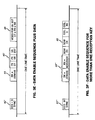
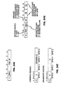
- the actual data for this tile 36 is presented in a series of lines, corresponding to the number of rows in the tile to be updated, following the data enable sequence line. Note that the correspondence is not one line to one tile row and is explained below. Similar examples are shown for the information having IID codes JSN416 and MDC2000 in FIGS. 3C and 3D, in which in the information having IID code JSN416, a tile of 1 row by 11 columns is updated, and again in MDC2000, a second tile of 6 rows by 40 columns is updated. Alternatively, as shown in FIG. 3E, the update data may appear on the same line as the data enable sequence. In particular, the sync signal 42' is followed by the IID code 44.
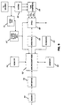
- the output of the microcomputer 52 is applied through an interface 55, to a digital video generation unit 56 which reconfigures the output of the microcomputer into digital video lines.
- the digital video generation unit 56 also generates the encoded signal flag and inserts the various synchronizing signals at the beginning of each of the digital video lines.
- a clock signal generator 57 is connected to the digital video generation unit 56 and the microcomputer 52 for applying timing signals thereto at the line frequency.
- a memory 58 is connected to the microcomputer 52 into which the pages or records are entered enabling the microcomputer 52 to compare one page or record with the update of the page or record to extract therefrom only the update data.
- the second concept is the use of implied motion where portions of financial market information contain regions that must be moved, either vertically (scrolled) or horizontally (panned).
- conventional financial instrument tickers are usually panned horizontally across a video screen, while news headlines are sometimes scrolled vertically.
- This movement can be accomplished by either retransmitting all of the required information such that the relative location of each column (panning) or row (scrolling) is adjusted for each incremental move, or in accordance with a preferred embodiment, by transmitting only the new information and "implying" the desired motion by the prior definition of a panning or scrolling tile type. Implied motion within a tile greatly improves the messaging efficiency.
- a video tile 250-V is used to display a realtime television program information signal.
- Each pixel within the video tile may take on any color supported by the relative television transmission standard and the picture store memory size of the given decoder 316.
- the decoder 316 includes a picture store memory, different TV signals may be selected for display within a video tile 250-V so long as they are being transmitted within the same vertical format. If, however, a picture frame memory is used, which can store an entire frame of television program information signals, then the video tile 250-V need not be limited to the same vertical format and may be located anywhere on underlying tile 350.
- the amount of required transmitted data to display the tile 251-G is reduced by a factor of approximately eight from 1,600 bytes to 198 bytes.
- the 1,600 bytes is based on 16 bytes per cell and 100 cells.
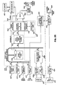
- Each decoder 316 includes an analog front-end signal processor (AFESP) circuit 610, which receives the DV bus signals, recovers a clock signal from the modulated signal and establishes detection thresholds for processing the quad level DV bus signals.
- AFESP analog front-end signal processor
- the output of AFESP circuit 610 is passed to demultiplexor (DEMUX) circuit 620, which demultiplexes the television program information signals and the digital-video signals, such that each may be further processed and provided to video screen 317.
- DEMUX circuit 620 passes the digital-video signals to demodulator circuit 630 which converts the quad level (8,9) modulated signals into binary signals.
- the cell change RAM 771 is operated in Read-Modify-Write mode.
- the contents of one cell 776 are read and numerically added, at binary adder 775, to the pixel change value that is supplied by the pixel comparator 760 for the corresponding cell 210 of display information.
- the weighted sum is then rewritten into the same cell 776 in the same cycle.
- each cell 776 acts as a cumulative counter that is incremented by the pixel change value from comparator 760 corresponding to the absolute value of the intensity change.
- the data in a given cell 776 of cell change RAM 720 is reset to zero when the RVC CPU 780 or the encoder 312 broadcasts the pixel change data corresponding to the given cell 776 to the encoder 312 or decoder 316 respectively.
- RVC CPU 780 is responsible for configuring all the various control registers within the RVC 400 and for retrieving and manipulating the pixel data in the indicated or identified cells 210 with changes. After a complete video frame has been digitized and compared, the CPU 780 is interrupted by the control logic 773.
- the CPU 780 software should be capable of detecting certain special case video changes. For example, a screen going completely blank should be detected and encoded without requiring direct messaging of each pixel.
- the Message Buffer 625 is a dual-ported static RAM device that can be accessed by both the Packet Reception ASIC 622 and the decoder CPU 690. Arbitration is provided by the conventional RAM control circuitry within the Message Buffer 625 to prevent simultaneous access. Messages that have been decoded and error corrected are compared against hardwired or previously enabled reception keys, which also are stored in the RAM of Message Buffer 625. Those messages that match reception keys are then loaded into the RAM of Message Buffer 625 from the Packet Reception ASIC 622. Once a complete message (that matches a reception key) has been loaded into the Message Buffer 625, the CPU 690 is notified via an interrupt from ASIC 622 over bus 623. The CPU 690 may then interrupt its normal program operation and retrieve the complete message from the Message Buffer 625.
- the mouse interface 684 provides a serial interface to, for example, four mice 319'.
- Mouse data is retrieved from the mouse interface 684 via the data bus 661D, once an interrupt has been received.
- the workstation must either be located at the trading desk or expensive cabling and signal amplifiers must be used to transport the mouse signal between the equipment room and the trading desk.
- the encoder and decoder information distribution system performs most mouse signal processing locally at the desk and when appropriate communicates the result to the equipment room via the multidropped control bus 318. This design also reduces the processing load on the host CPU 425.
- Dragging is the process of holding down a mouse button while moving the mouse.
- Most mouse applications do not drag the "contents" of the window. That is, the window and its contents remains stationary while a new temporary substitute marquee border is drawn and moved across the video screen.
- the button is released the temporary substitute marquee border is removed and the contents of the window are redrawn at the new location on the screen.
- the contents of the window are not continually redrawn as it is dragged across the page to reduce the amount of CPU processing that would be required to constantly rewrite the video memory.
- Applications that redraw the contents while being dragged significantly load the CPU as evidenced by the inability of all but the fastest machines to keep up with rapid dragging. It is not practical to have a single host CPU machine process multiple composite pages of window-dragging simultaneously unless this border substitution methodology is employed.
Description
- The subject invention relates to the distribution of information and, more particularly, for distributing this information in a secure and restricted manner to a plurality of users.
- Applicant and other related companies are in the business of distributing realtime financial market information to various clients who use this information to carry on their business. When a client subscribes for this service, an agreement is entered into in which the client indicates what information is desired and how many video screens will be displaying the information. Based on these parameters, a fee is assessed to the client and the information then is transmitted to the client.
- Typically, this financial market information is transmitted to clients as one or more pages or records that may be displayed on a video screen, portions of which, from time to time, are updated to reflect changes in the market information. Various clients subscribe to view different specific groups of these pages and/or records.
- An early method of distributing market information was based upon the transmission of a single page of real time digital information over a single telephone line. Page-oriented information (ROW #, COL #, CHARACTER STRING) was sent from the information vendor's computer over a telephone network to a controller, provided by the information vendor, located at the client site. The page-oriented information was subsequently converted to video by a video generation unit within the controller. The video output was then connected to a video screen by a single coaxial cable.
- Each full page was repeatedly transmitted in video at a field rate for realtime display, similar to that of a television transmission. However, once the video signal was produced, there was nothing, except the personal integrity of the client, to prevent the client from connecting any number of video screens to a video distribution amplifier connected to the controller, driving a larger number of video screens above and beyond the number stated in the agreement. This practice dilutes the revenues to which the information vendor would ordinarily be entitled.
- This architecture was costly and unreliable because of the large amount of hardware needed to place financial information on a large number of trading desks. For example, if a client's trading room had thirty traders, each trader needed his own single-user system resulting in thirty keyboards, thirty controllers with thirty internal video generation units, thirty telephone cables, thirty modems, thirty coaxial video cables, and thirty video screens to receive and display the required financial information.
- This technology also limited the screen presentation format to what was provided by the information vendor. When traders were only interested in one or two fields of information on a screen, they would have to display the entire page of information. If they wanted to look at one or more fields of information on a second screen at the same time, an entire additional single-user system would be required. Further, when two traders wanted to look at the same page, they would either have to have two separate single-user systems or the video information would be redistributed to a "slave" video screen making it difficult for the information vendor to know how many video screens were connected to a given controller and hence how many people were viewing their information. This made billing difficult and usually created a process of surprise client-site visits that left both information vendor and client unhappy.
- The development of multi-user systems reduced the amount of required hardware and enabled users to share resources and view common information. In multi-user systems, each trader had one keyboard and several video screens. Through the use of video switching techniques, thirty traders could share perhaps ten or fifteen controllers and contend for their use. Since many traders are part of a trading group that uses essentially the same financial market information, the probability of blocking (not having a controller available to fulfill a new page request) was small.
- Such multi-user systems helped reduce costs by reducing the number of controllers, keyboards, and system cabling, but did not solve either the billing problems or allow the user to customize screen presentation formats.
- Later, single telephone line, multi-page distribution systems were developed which reduced the required number of telephone lines. The information syntax for these multi-page sources was slightly modified to (PAGE #, ROW #, COL #, CHARACTER STRING). Users of such systems also could create composite pages (fields from different pages displayed simultaneously on one video screen) and calculate and insert additional value-added information (e.g., bond yield to maturity). By doing so, customized output display pages could be created showing only the information and value-added calculations the user wanted to see.
- Users developing value-added applications based upon page oriented data had to assign a symbolic name to an information field located at a specific display location of the input source page. When the information vendor changed the presentation format of the information (i.e., the location of a specific data element), as often happens when financial instruments are either added or deleted, the value-added application had to be modified. To overcome this difficulty, and to supply basic information without display parameters, the information vendor created record-oriented sources using the syntax (SYMBOLIC NAME, CHARACTER STRING). Examples of such a system are the Reuters Integrated Data Network and the Telerate TIQ Feed.
- Despite the foregoing advances in the field of electronic financial information distribution systems, current systems still allow video screens to be added and/or moved freely without either the information vendor's knowledge or consent. Further, each video screen must be connected by its own single-video "home-run" cable, i.e., a cable that typically runs for hundreds of feet between the trading floor where the video screen is located and the equipment room where either a controller, video switch output, or a host computer is located.
- An object of the present invention is to provide a system capable of securely providing restricted information.
- A further object of the present invention is to provide a system which is capable of uniquely identifying each of the video screens authorized to display information, to restrict this information to only these individual video screens, to identify which of the information these video screens are to display, and to present only authorized information on each and every video screen; unauthorized video screens would only present unintelligible transmogrified versions of the information.
- It also is a object of the present invention to provide a financial information distribution system that is capable of taking inputs simultaneously from both multiple information page and/or record-oriented input sources (e.g. video, digital and/or live television) and a multitude of keyboards, to create a multitude of different output displays for concurrent display on a multitude of video screens all interconnected by a single cable, such that the video screens may contain different combinations of portions of different input sources of information.
- It is a further object of the present invention to provide a financial information distribution system in which each video screen has a unique display identification code that is used to authorize viewing and/or to permission what input source information each individual video screen will be capable of displaying at any given time.
- It is a another object of the present invention to facilitate the ability to provide each user's video screen(s) with a customized output display.
- It is yet another object of the present invention to reduce the cost of transmitting and displaying financial market updates to numerous users.
- It is further object of the present invention to provide a single host computer device to support a plurality of users and an even larger plurality of video screens for securely distributing restricted information to one or more authorized video screens simultaneously. It is another object to allow rapid response to user requests to view new or additional source of information.
- It is another object to provide for distributing information in a tile format whereby each user can assign a location on that user's video screen for display of the tile, and the same display information may be displayed on different locations on different video screens and simultaneously updated. It is another object to support a larger video screen to provide for displaying tiles from a plurality of information input sources simultaneously.
- Applicant has recognized that usually only small portions of the input page or record source information change over a small time, for example, the time corresponding to one field time of displayed video. It is, therefore, necessary to transmit only the information which is changing as update data and then to store this update data, along with the unchanged data, in a memory at the video screen for subsequent display.
- It is, therefore, another object to preprocess video signals to identify the changed display information to be displayed prior to inputting the video information into a display information distribution system, thereby minimizing the amount of channel bandwidth to distribute the information.
- It is another object of the invention to provide for preprocessing digital and analog video signals for display information including financial market information and television program information signals.
- The present invention is defined in the claims to which reference should now be made. Preferred features are laid-out in the subclaims.
- The above objects are achieved in a system for securely providing restricted information, wherein the system includes an encoder for encoding update data for updating various tiles (i.e., portions of pages or records) of display information, and a plurality of decoders for decoding said update data and generating said various output displays on video screens, characterized in that said encoder comprises means for generating a first data stream, said first data stream including respective sets of one or more unique display identification codes identifying each video screen and one or more information identification codes for each of said tiles, said sets being indicative of the tiles, i.e., each particular portion of display information, each video screen of each client or user is authorized to receive; means for generating a sequence of second data streams, each of said second data streams including one of said individual information identification codes, coordinates of an area in a relevant video screen that is to display update data for the portion of display information, and the respective update data; and means for transmitting said first data stream followed by said sequence of second data streams; and in that each of said decoders comprises a video screen; means for identifying the relevant video screen with one of said unique display identification codes; means for recognizing said one unique display identification code and for storing the information identification codes in the associated set with said one unique display identification code; means for retrieving said display coordinates of the update data corresponding to each of said stored information identification codes; means for storing said update data at the related coordinates for subsequent display on the video screen; and means for selectively displaying said stored updated display information on the video screens.
- In accordance with a preferred embodiment, the encoder (also referred to as a transmitter) is a microprocessor based device that transmits a high bandwidth digital and/or analog signal over a single coaxial cable. The encoder manages communications between a host computer and the plurality of decoders (also referred to as receivers), caches those particular portions of display information that are being viewed on video screens, and stores symbolic data elements. All data changes and/or specific instructions sent to any one or all of the decoders originates in an application running on the host computer, and is transmitted via a digital-video (DV) bus from the encoder to the decoder(s). A delta-modulation type of communication protocol is used to greatly reduce the amount of transmitted information. Unlike a video switch environment, in which almost the same information is transmitted sixty times a second, only display screen changes are signaled.
- Display changes are transmitted by tile messaging, i.e., transmitting the portion of the page or record of financial market information that contains the changed financial market information within a tile of horizontally and vertically ccntiguous cells. Each tile is given an information identification code and has corresponding data such that authorized users of the data are enabled with the corresponding information identification code as a symbolic name or reception key for identifying the particular tile by its symbolic name or reception key and receiving and retrieving the update data. Further, the tile may be given a default size and display location on a video screen, a user-defined size and display location, or both, such that the transmitted data is mapped into any user-defined location as it is stored for display on the video screen. Some of the transmitted data may not be stored or displayed when the user-defined tile is smaller than the transmitted tile.
- The cost associated with transmitting the same data for different tiles (pages or records) of information can be greatly reduced in accordance with the present invention, by initializing the location of an individual data field, through the use of a message identifying (i) the information identification code for a particular source page or record of display information, (ii) the information identification code for the specific information field through the use of a symbolic name of a tile containing the individual data field, and (iii) a location in which the data of the data field are to appear on the particular tile. After this initialization, the information identification code for the symbolic name can be transmitted along with data, without any display coordinate information, and each initialized video screen that displays the data associated with the symbolic name is updated simultaneously through the use of this single data message and previously provided display coordinates.
- Each decoder receives at least all transmitted messages for its video screens and stores the information to be displayed, i.e., the screen image, in an internal picture store memory. Each decoder selects out and processes only those messages on the DV bus that are directed to its video screens or to the decoder. Thus, each decoder may have more than one video screen and a unique display identification code for each video screen. Each video screen has a unique identification code that supports permissioning of restricted display information to be viewed and is capable of displaying simultaneously either color or monochromatic text and/or pixel based graphics, as well as live TV pictures. In addition, the decoder can detect and directly pass through unencoded video signals to its video screens.
- Commercially available keyboards and mice may be provided to send information request signals via the decoder to a control bus connecting the plurality of decoders to the encoder or host computer and to define tile size and display locations. The keyboard optionally may include an internal LCD display.
- A residual video converter (RVC) device allows both view-only and interactive video sources to be utilized on the system. The RVC device accepts one or more video inputs, converts them into a DV bus message format containing only video screen changes suitable for transmission to the decoders over the DV bus, and directly interfaces with the encoder. Thus, the encoder may transparently pass the RVC output signals at appropriate times.
- A television feed converter (TFC) device allows realtime television sources to be utilized on the system. The TFC device accepts one or more television inputs, converts them into a format suitable for transmission to the decoders over the DV bus, and directly interfaces with the encoder. The encoder may transparently pass the television program information signals at appropriate times.
- In addition, financial market information may be brought into the system via a commercially available Digital Interface Board (DIB) device. On larger systems, the DIB device also may be configured to manage the control bus. The DIB device also allows for authorized individuals to gain remote access to the system, for example, by use of passwords. For example, the information vendor may use the interface remotely to "authorize" clients to use and/or view predefined subsets of their source information (e.g., to increase the number of authorized video screens). The vendor also is able to gather utilization statistics from each client site which is useful for marketing and/or billing purposes. The operator of the system may use the interface remotely to provide routine software maintenance and upgrades, modification of existing composite page definitions, downloading of new composite pages and periodic monitoring of system performance. The client system administrator may use the remote interface to log onto the system from home or any other remote location.
- One advantage of the present invention is that it is sufficiently flexible to adapt for use as any of a stand-alone system in a small system environment having only a digital data feed which the encoder distributes to a plurality of decoders, an enhancement to an existing system having a video switching system and user interface hardware such that the encoder output is connected to a single shared input and passed to one or more outputs on the video switch to the plurality of users, a work station, and a large system including, for example, separate machines for providing value-added calculations.
- With the above and additional objects and advantages in mind as will hereinafter appear, the invention will be described with reference to the accompanying drawings, in which:
- FIG. 1 is a block diagram of a system according to the invention;
- FIG. 2 is a diagram representing the transmitted first data stream and the sequence of second data streams in a first embodiment of the invention;
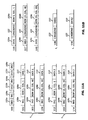
- FIG. 3A shows a diagram representing a characteristic first data stream, and FIGS. 3B-3F show diagrams representing characteristic sequences in the second data streams, all in the first embodiment of the invention;
- FIG. 4 shows a video screen having a sample market information page thereon in which a block of data to be updated is shown in cross-hatch;
- FIG. 5 shows a block diagram of an encoder in the system according to the first embodiment of the invention;
- FIG. 6 shows a block diagram of a decoder in the system according to the first embodiment of the invention;
- FIG. 7 is a diagram representing the transmitted video signals in a second embodiment of the invention;
- FIGS. 7A-7C illustrate the technique of transmitting and displaying a plurality of television program information signals along with update data;
- FIG. 8A shows a diagram representing the transmitted first data stream, and FIGS. 8B and 8C show diagrams representing the second transmitted data stream in the second embodiment of the invention;
- FIG. 9 is a block diagram of an encoder in a second embodiment ;
- FIG. 10 is a block diagram of a decoder in a second embodiment ;
- FIG. 11 is a block diagram of a system according to a third embodiment ;
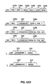
- FIG. 11A-11C illustrates the transmission of enable reception messages, enable reception and initialization messages, initialization messages, and data enable sequences to produce the displays illustrated in FIGS. 12A - 12C illustrating symbolic signaling;
- FIG. 11D is a flow chart for processing messages using symbolic signaling according to one embodiment of the present invention;
- FIG. 12 is an illustration of the format for a single page of display information in accordance with the invention;
- FIGS. 12A-12C illustrate the displays produced through the message sequences shown in FIGS. 11A-11C, as described above;
- FIG. 13 is an illustration of a composite page having a plurality of tiles;
- FIG. 13A-13C are illustrations of tile messaging for updating different user defined tiles having common display information;
- FIGS. 14A and 14B are illustrations of composite pages of display information;
- FIG. 15 is an illustration of graphic tile messaging with graphic and alphamosaic cells;
- FIG. 16 is a block diagram of DV bus signaling for the embodiment of FIG. 11;
- FIG. 17 is a diagram of a DV bus message stream over two successive video signal time periods;
- FIG. 18 is a diagram of a quad level (8,9) modulated signal for a DV bus message;
- FIG. 19 is a diagram of a header section of a digital message using the quad level (8,9) modulation;
- FIG. 20 is a diagram of a double buffered error detection and correction interleaving technique;
- FIG. 21 is a diagram of a packet messaging sequence including packets of varying length;
- FIG. 22 is a diagram illustrating packet fields;
- FIG. 23 is a diagram illustrating message fields;
- FIG. 24A-24G are diagrams of control bus messaging signals;
- FIG. 25 is a block schematic diagram of the encoder of FIG. 11;
- FIG. 26 is a block diagram of a desk interface unit.
- FIG. 27 is a block schematic diagram of the decoder of FIG. 11;
- FIG. 28 is a block schematic diagram of the video output circuit of FIG. 27;
- FIG. 29 is a block diagram of a modular residual video converter device ; and
- FIG. 30 is a block schematic diagram of the video digitizer circuits of FIG. 29.
-
- As noted above, the object of the present invention is to distribute information. This information is transmitted over, for example, telephone lines and converted on the client site into video signals similar to those for television reception. The information subscribed to takes the form of pages or records of market data, various portions of which are updated from time to time to reflect changes in the market, and subsequently presented on a video screen.
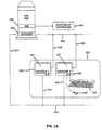
- In a first embodiment of the invention, the signals representing the market information are being transmitted asynchronously, that is, there are no set characteristic times (e.g., television field or frame rates) to restrict the transmission. As shown in FIG. 1, one or more portions of
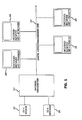
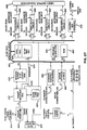
source information 10 of market data are each given individual information identification (IID) codes, for example, "JSN416" and "MDC2000". Theseportions 10 are then applied by an encoder-transmitter 12 to a digitalvideo transmission line 14. Decoder-receivers 16 are shown connected to thetransmission line 14 for receiving and displaying the encodedportions 10. As shown, eachdecoder receiver 16 has a unique display identification (DID) code, for example, "PAMU0609", "BOBO1205", "LRN0122" and "TBD12??". - FIG. 2 shows a diagram representing the digital video signals transmitted over the digital
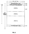
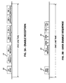
video transmission line 14. As shown in FIG. 2, afirst line 20 of the transmission includes an encoded signal flag indicating to the decoder-receivers 16 that the following information is encoded data. The exact form of the flag is unimportant since the information contained is just one bit. The line orlines 22 contain enable reception messages. Thelines 24 following the enable reception message lines 22, contain thevarious data updates - Enable reception messages are used to provide information identification (IID) codes or reception keys (RK) to decoders. The terms "information identification codes" and "reception keys" are used interchangeably. Decoders use reception keys to identify the portions of information that are to be displayed on specifically identified video screens. FIG. 3A shows a representative enable reception (ER)
message line 22 in detail. AnER synchronizing signal 32 is sent indicating the ensuing transmission of enable reception messages and enabling decoders to synchronize to the transmission. TheER sync signal 32 is followed by display identification code (DID) - reception key (RK) sets 34, each of which includes at least one of the unique DID codes and at least one of the IID codes as a reception key (RK) for which the video screen identified by the decoder-receiver DID is authorized to display. In the example shown, the sets are the DID/RK pairs TBD12??/MDC2000, BOBO1205/JSN416 and LRN0122/MDC2000 and indicate that the video screen connected to the decoder-receiver having the DID code TBD12?? is authorized to display update data for the source information corresponding to RK MDC2000, screen DID BOBO1205, RK JSN416; and screen DID LRN0122, RK MDC2000. It should be noted that in the example, the video screen for the decoder-receiver having DID TBD12?? is not authorized to display update data for the source information corresponding to RKs JSN416 and MDC2000. The enable reception message continues for as many lines (each including an ER synchronizing signal 32) and includes asmany sets 34 as are required to associate each of the authorized video screens, by their decoder-receiver DIDs, with one of the (many) subscribed-to groups or portions of source information by their information identification codes/RKs. - The process for updating each output display is performed by replacing "tiles" in the relevant output display. As shown in FIG. 4, the
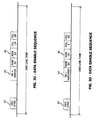
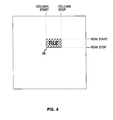
cross-hatched tile 36 to be updated is located by two row and two column (or two x-y pixel pair) coordinates. FIGS. 3B - 3F show samples of the data enable sequences, in which, in FIG. 3B, the sequence for the update of information having the IID code MDC2000 is illustrated. In particular, adata synchronizing signal 42 indicates the ensuing transmission of a data enable sequence, and is followed by theIID code 44 for the source of information having IID code MDC2000 and then thecoordinates 46 of thetile 36 to be replaced which, in this example, is 4 rows by 40 columns. The actual data for thistile 36 is presented in a series of lines, corresponding to the number of rows in the tile to be updated, following the data enable sequence line. Note that the correspondence is not one line to one tile row and is explained below. Similar examples are shown for the information having IID codes JSN416 and MDC2000 in FIGS. 3C and 3D, in which in the information having IID code JSN416, a tile of 1 row by 11 columns is updated, and again in MDC2000, a second tile of 6 rows by 40 columns is updated. Alternatively, as shown in FIG. 3E, the update data may appear on the same line as the data enable sequence. In particular, the sync signal 42' is followed by theIID code 44. However, the coordinates 46' include the pixel start number and the pixel stop number of a single row of the update data, along with the line number of the particular line. Theupdate data 48 then follows on the same line. Eachtile 36 is then composed of theupdate data 48 appearing in, for example, a plurality of consecutive lines. Further, as shown in FIG. 3F, the update data may be presented simultaneously on one line for more than one page at a time. In particular, thesync signal 42" is followed by twoIID codes 44", and then thecoordinates 46 of thetile 36 to be replaced, which in this example, is 5 rows by 80 columns, toward the bottom of the portions of information having IID codes JSN416 and MDC2000. Additionally, all authorized displays connected to the video transmission may be simultaneously updated at the same coordinates by using a special reception key, e.g., RK = 0. - An encoder for the first embodiment of the invention is shown in FIG. 5. The encoder includes a
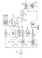
modem 50 for receiving data from a source of market information. This data may be in the form of entire pages or records of financial information where portions are updated, or the update data itself along with information for the positioning of the update data on the respective display screen. The output ofmodem 50 is connected to aninterface 51, which is, in turn, connected to the input of amicrocomputer 52. Themicrocomputer 52 reassigns the data to appropriate locations in new output displays for clients of the information vendor. Akeyboard 53 is connected to themicrocomputer 52 for controlling the microcomputer. Amemory 54 is connected to themicrocomputer 52 and supplies thereto the configuration of the new output displays, the reception key (RK) codes for each of the new portions of display information, and the display identification (DID) codes of the client's video screens authorized to receive each of the new portions of information. Based on this information, themicrocomputer 52 generates the first data stream and the sequence of second data streams. - The output of the
microcomputer 52 is applied through aninterface 55, to a digitalvideo generation unit 56 which reconfigures the output of the microcomputer into digital video lines. The digitalvideo generation unit 56 also generates the encoded signal flag and inserts the various synchronizing signals at the beginning of each of the digital video lines. Aclock signal generator 57 is connected to the digitalvideo generation unit 56 and themicrocomputer 52 for applying timing signals thereto at the line frequency. In the event that the update information applied to themodem 50 is in the form of entire pages or records, amemory 58 is connected to themicrocomputer 52 into which the pages or records are entered enabling themicrocomputer 52 to compare one page or record with the update of the page or record to extract therefrom only the update data. - FIG. 6 is a block diagram of a decoder for use with the encoder of FIG. 5. The decoder includes a
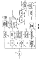
receiver 60 for receiving the data transmitted by the digitalvideo generation unit 56. The output of thereceiver 60 is applied to ananalog switch 61 for selective application to a video screen in the event that standard non-coded signals are being received. Acoded signal detector 62 is coupled to thereceiver 60 for receiving the encoded signal flag and for switching theanalog switch 61 accordingly. AnER detection gate 63 is connected to thereceiver 60 for receiving the enable reception messages containing the DID/RK code sets. Each of the received DID codes is compared with a unique display identification code stored in aROM 64 by acomparator 65. Upon each match of the DID code, the individual RK code for the respective portion of information is stored in amemory 66. - The output of the
receiver 60 is further connected to adata detection gate 67 for receiving the data enable sequences. The individual RK codes in the received data enable sequences are compared in acomparator 68 with the individual RK codes stored in thememory 66. Upon a match of one of these RK codes, the accompanying display coordinates of the update data are loaded into registers 69. An analog-to-digital converter 70 processes the appropriate update data at the output of thereceiver 60 and applies its output to awrite buffer 71, which also receives the output of theregisters 69. The output of thewrite buffer 71 is applied to apicture store memory 72 in which the section therein corresponding to the location of the update data is updated by using the display coordinates. A synchronizingsignal detector 73 is connected to the output of thereceiver 60 for separating the message synchronizing signals. The output of the synchronizingsignal detector 73 is applied to a timing and controlsignal generator 74 for generating timing signals for the analog-to-digital converter 70, thedata detection gate 67, theER detection gate 63 and thepicture store 72. The output of thepicture store 72 is applied to a digital-to-analog converter 75 controlled by the timing and controlsignal generator 74. The output of the digital-to-analog converter 75 is applied through a low-pass filter 76 to another input of theanalog switch 61. - In a second embodiment of the invention, the video signals representing the market information includes color information. In addition, standard television program information signals are included in the digital video signals for selective viewing of realtime television programs on the video screens. This transmission is necessarily synchronous to the chosen television standard. When the digital video signals are being transmitted by coaxial cable, the usable bandwidth is in excess of 24 MHz.
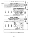
- FIG. 7 shows a pictorial representation of the transmitted video signals. The encoded
signal flag line 80, the enable reception messages lines 81 and the data enablesequence lines 82 are transmitted during thevertical blanking interval 83 between each field of the video signal. During the active video portion of the field, in a first half of each scanning line, the television R, G and B signals 84, each originally having a bandwidth of 4 MHz and each time compressed by a factor of six to an expanded bandwidth of 24 MHz, are sequentially transmitted. In the second half of each scanning line, the update data for individual pages of the market information are transmitted. While the television program information signals 84 are in color, the update information may be monochromatic, color or a mixture of both. In particular, as shown, the first 8 half-lines contain themonochrome update data 85 for the left half and right halves, respectively, corresponding to RK code MDC2000. Theupdate date 85 is followed by theupdate data 86 corresponding to RK code JSN416. Theupdate data 86 is presented in color as the three color signals R, G and B. The remainder of the right half of the first field is shown as being unused in this example. The left half of the second field contains the G, B and R components of the television program information signals 78'. The right half of the second field contains the monochromatic update data corresponding toRK codes - FIGS. 7A - 7C illustrate the technique of transmitting and displaying more than one television program information signal at a time along with update data for output displays on a plurality of video screens. Specifically, FIG. 7A illustrates the transmission of four fields of digital video signals corresponding to two television video frames. A
vertical blanking interval 83, corresponding to thevertical blanking interval 83 of FIG. 7, is shown. Nine different sources of information are shown as being transmitted in the fields, namely television program information signals TV1-TV3 and six tiles numberedTILE 1 toTILE 6 having corresponding update data to particular portions of financial market information. The transmission of a field structured in this manner is done at the television scanning rate, as mentioned above. - The television program information signals TV1-TV3 are shown as being time compressed in a well known manner. The TV1 signals are shown as being transmitted during a portion of every horizontal digital video line. Television program information signals TV2 and TV3 are shown as being transmitted only during certain horizontal digital lines, namely from line W to line X, in the case of TV2, and from line Y to line Z, in the case of TV3. The television program information signals TV1-TV3 are shown as pluralities of lines having alternating odd line (TVODD) and even line (TVEVEN) fields in successive video fields. The television program information signals are illustrated in FIG. 7A in the RGB format, i.e., three primary color signals, but also may be transmitted as one luminance and two color difference signals, e.g., Y,U,V. Further, the television program information signals may be digitized and compressed, e.g., using the JPEG or MPEG standards or some other technique.
- Also, the update data to output display tiles TILE 1 -
TILE 6 are transmitted in various lines at times when the television program information signals are not being transmitted. - The update data for an output display tile may appear anywhere in the video screen and may start and stop at any point or in any line of the digital video field, provided that the update data does not occur simultaneously with the television program information signals. Thus, update data may occur during the
vertical blanking interval 83 as shown in the third digital video signal field for update data toTILE 3. Update data also may be a lengthy stream of data that fills those portions of successive lines that are not filled by television program information signals as illustrated in the fourth digital video signal field with respect to the update toTILE 2 and signals TV1 and TV2. Further, update data may be a relatively short stream of data starting at the beginning of a line time, or in the middle of a line time, see, e.g., updates toTILE 6 andTILE 2 andTILE 1 in the fourth field. - In addition, there may be no update data for financial market information as in the first digital video signal field containing television program information signals TV1ODD, TV2ODD, TV3EVEN, although there will be some digital data (not shown in the first field) that is transmitted, as described below.
- The resulting displays that are possible with this transmission structure are illustrated in FIGS. 7B and 7C and 13. FIG. 7B illustrates the display of the television program information signals TV1 and which, due to the transmission of such signals during each digital video scan line, produce full screen television displays. FIG. 7C, on the other hand, illustrates the display of both TV2 and TV3 signals which, by virtue of their transmission within the stated intervals, are displayed within specific vertical boundaries within the video screen. Specifically, the TV2 display must be located between horizontal lines W and X in any horizontal location (with the proviso that it not interfere with output display data) and TV3 must be displayed between horizontal lines Y and Z, in any horizontal location (with the same proviso). The output display corresponding to one of the source information in tiles TILE 1 -
TILE 6 that the particular video screen is enabled to receive can be displayed above, below or alongside the TV2 and TV3 signals (only TILE 1 -TILE 3 are illustrated). - Due to the complex ordering of the update data in the first and second fields, the data enable sequences in the
lines 82 must necessarily be more complex than those shown in FIGS. 3B - 3F. In addition, the enable reception messages also must indicate which of the video screens is authorized to receive the television program information signals sent with the update data. In particular, as shown in FIG. 8A, the enable reception messages are similar to those shown in FIG. 3A, with the exception that in addition to the DID/RK code sets, the messages include aset 87 indicating which of the video screens, for example, the screen with DID code 297, is authorized to receive which television program information signals, for example, the television program information signal having an IID code TV1, which also may be used as a reception key (RK) if distribution is to be enabled. FIG. 8B shows a sample data enable sequence which includes, in addition to that described with respect to FIGS. 3B - 3F, the coordinates of the update data in the source field. FIG. 8C shows a sample of the data enable sequence for identifying the television program information signals, and includes adata synchronizing signal 88, atelevision RK code 89 and the starting coordinates 90 of the color signals, red, green and blue, or Y,U,V. - FIG. 9 shows a block diagram of an encoder for the second embodiment. The digital video generation unit 56' has a second set of inputs for receiving the three components of the color television program information signal, Y,CD1,CD2. In particular, a source of television program information signal is connected to a synchronizing
signal separation circuit 91 for detecting the vertical and horizontal synchronizing signals in the video signals. The source of the video signals is also connected to amatrix circuit 92 for providing the three components. Each of these components is subjected to compression incompression circuit 93 and the three components are then applied to the digital video generation unit 56'. The clock and sync signal generator 57' applies synchronizing signals to both the digital video generation unit 56' and the microcomputer 52', and receives the synchronizing signals from theseparation circuit 91 for synchronization therewith. - FIG. 10 shows a block diagram of a decoder for the second embodiment. Components the same as those in FIG. 6 are designated with the same reference number. The decoder is substantially similar as the decoder of the first embodiment with the exception that the decoder is now capable of processing color signals and the encoded data selectively includes television program information signals. In particular, a
color decoder 101 is included between the output of thereceiver 60 and the input of the analog switch 61.1 - 61.3. The register 69' includes a register element for storing the number of the picture store. The synchronizing signal detector 73' outputs field synchronizing signals in addition to line synchronizing signals. Thewrite buffer 71 now accesses three picture stores 72.1 - 72.3 corresponding to the three color components, red, blue and green. The outputs of these picture stores 72.1 - 72.3 are applied to three digital-to-analog converters 75.1 - 75.3, and then to three low pass filters 76.1 - 76.3 for application to the other inputs of the three analog switches 61.1 - 61.3. - Referring to FIGS. 11 to 29, a third embodiment is shown, which reflects a number of improvements to the first and second embodiments described above. One system in accordance with the third embodiment includes an
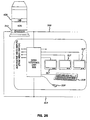
encoder 312, a digital-video (DV)bus 314, a plurality ofdecoders 316, a plurality ofvideo screens 317, acontrol bus 318, akeyboard 319, optionally a mouse 319', and a supply (or source) ofdisplay information 310 which may include realtime television program information signals, and analog and digital video signals representing financial market information. TheDV bus 314 is preferably a channel capable of transmitting digital and video information. This permits the use of standard coaxial cables or video switches as theDV bus 314. - As illustrated in FIG. 11, each
decoder 316 has an associatedvideo screen 317, preferably constructed as an integral unit in a common enclosure. Alternately, as shown in FIG. 26, eachdecoder 316 may be part of a desk interface unit (DIU) 321, which supports a plurality ofvideo screens 317, e.g., four, and a plurality of users and theirrespective keyboards 319 and mice 319'. Each user may have one ormore video screens 317 arranged in a work space, e.g., on adesk top 320. Each video screen may have a unique DID. Alternately, each user ordesk top 320 may have a unique DID such that restricted display information may be displayed on any video screen of the enabled user or desktop. - One aspect of the present invention concerns improvements in the structure of the signals (also referred to as "DV bus signals" which are concatenated to form "DV bus messages") and their messaging along the
DV bus 314 between theencoder 312 and the plurality ofdecoders 316, and their display on avideo screen 317. - FIG. 12 illustrates the image produced on each
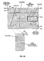
video screen 317, which is acomposite page 200 of financial market information and/or television program information signals, as described below. Each composite page is organized as a plurality ofcells 210. Each cell is organized as a plurality ofpixels 220. Everycell 210 has an assigned location withincomposite page 200, by row R and column C, relative to an origin and cannot be arbitrarily placed. The origin may be selected to be in the upper left corner or elsewhere. Similarly, everypixel 220 has an assigned location within eachcell 210, by row r and column c, relative to a cell origin and cannot be arbitrarily placed. In accordance with the present invention, and as explained below, messages transmitted alongDV bus 314 are either directly or indirectly addressed to cells. - In a preferred embodiment, each
composite page 200 is composed of 30 rows and 100 columns of uniform and fixed-sizerectangular cells 210, as shown in part in FIG. 12. The coordinates of thecell 210 in the upper left corner of thepage 200 are (R0,C0). Thecell 210 in the lower right corner of thepage 200 is at (R29,C99). Each fixed-size cell 210 has 128pixels 220 organized into 8 columns by 16 rows. This represents adisplay screen 317 that is larger than the size of standard pages or records of financial market information provided by commercial information vendors, and the size video screens provided by those vendors with their systems. Such standard pages and display screens have 18 or 25 rows by 80 columns or 12 rows by 64 columns. Advantageously, the larger display screen permits the user to createcomposite pages 200 containing more financial market information than previously possible with the prior systems, and further permits displaying television program information signals and/or value added information without sacrificing the financial market information. - Each
pixel 220 within acell 210 may have up to 256 different colors, selected from a larger palette of 16,777,216 colors. The number of colors that may be displayed on any givenvideo screen 317 depends on the amount of memory of thedecoder 316 operatively connected to the video screen. For example, if a decoder has been loaded with one byte per pixel of screen store memory, or approximately (800x480 = 384,000 pixels) 376 Kbytes of memory, it can display 256 colors per pixel. For another example, if a decoder, which has lower cost and functionality, has been loaded with only two bits per pixel of screen store memory, or approximately 96 Kbytes of memory, it can only display 4 colors per pixel. - Reducing the number of colors to be signaled also reduces the length of the messages needed to create or "paint" a
composite page 200. For example, when four colors are being used, only the first two significant bits of a color byte need be transmitted. Even when 256-color decoders are used, clever selection of the color definitions can reduce the amount of messages necessary to transmit information concerning a small tile on the page. For example, a first tile may havecolors colors - In this third embodiment also, DV bus messages are transmitted as tiles. As already noted, a tile is a rectangular region that will appear on the
video screen 317 and is illustrated here by the boldblack rectangle 250 on the right side ofcomposite page 200 in FIG. 12. It may contain any number of horizontally and verticallycontiguous cells 210. Preferably, each tile is defined by the location of its first cell, i.e., the coordinates (row R and column C), in its upper left corner and either its size (i.e., number of rows and columns of cells in the tile) or the coordinates of the cell in its lower right corner. - This third embodiment of the invention preferably employs two concepts of tile messaging to reduce further the amount of overall data that is required to be transmitted. The first concept is called cell wrapping. This provides for sending one large single continuous message to a tile for one
cell 210 after another (either horizontally or vertically aligned) within a tile having determined boundaries so that the first cell to cross the tile boundary in the direction of continuity automatically "wraps back" within the tile to the beginning of the next row or column so that each cell is successively filled. The tile boundaries are preferably incorporated into the tile display boundary coordinates provided to the decoder for the update data. This avoids having to monitor when thenext cell 210 will be outside of a boundary of the tile and resend either a new message or next row or next column indicator. The decision to use horizontally aligned messages or vertically aligned messages may be based on the aspect ratio of the tile boundary so as to minimize the number of wrapping events and maximize painting speed. When combined with run length encoding of messages, described below, cell wrapping greatly improves messaging efficiency. - The second concept is the use of implied motion where portions of financial market information contain regions that must be moved, either vertically (scrolled) or horizontally (panned). For example, conventional financial instrument tickers are usually panned horizontally across a video screen, while news headlines are sometimes scrolled vertically. This movement can be accomplished by either retransmitting all of the required information such that the relative location of each column (panning) or row (scrolling) is adjusted for each incremental move, or in accordance with a preferred embodiment, by transmitting only the new information and "implying" the desired motion by the prior definition of a panning or scrolling tile type. Implied motion within a tile greatly improves the messaging efficiency.
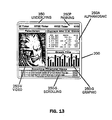
- Referring to FIGS. 12, and 13, the
video screen 317 may be referred to as theunderlying tile 350. One top of theunderlying tile 350, one or more of the following types of tiles, referred to astile 250 with a letter suffix, can be displayed as illustrated in FIG. 13. - A graphic tile 250-G may be defined to display information on a pixel by pixel basis. It is used to display graphs, charts, scanned images, e.g., still pictures, value-added presentations of historical data, and similar non-alphanumeric character display information.
- An alphamosaic tile 250-A is a tile entirely defined by an extended set of ASCII characters or the equivalent (i.e., alphanumeric characters). It is used to display normal alphanumeric character text plus any predefined extended ASCII characters. Each pixel usually may have up to 256 colors. In FIG. 13, the alphamosaic tile 250-A is illustrated as displaying information concerning U.S. Government securities that are periodically updated. Alphanumeric tiles 250-A are static unless they are further defined for relative movement.
- A panning tile 250-P is an alphamosaic tile that is controlled to create horizontal motion, left or right. In FIG. 13, panning tile 250-P is illustrated as the (NYSE) Ticker which is being panned right to left. The character string update "NYSE" has been received at the entry (partial "S" character) and is being automatically panned (partial "E" character) under the control of
decoder 316 using implied movement. The panning effect may be a cell by a cell advance or a pixel by pixel advance, the latter providing a smoother image transition and presentation of partial characters. - A scrolling tile 250-S is an alphamosaic tile that is controlled to create vertical motion, up or down. In FIG. 13, the scrolling tile 250-S is illustrated as the "Financial News" and is being scrolled upwardly. The entire lower row of characters has been received at the entry and is being automatically scrolled (partial top and bottom rows) under the control of
decoder 316 using implied motion. The scrolling may be a cell by cell advance or pixel by pixel advance, the latter providing a smoother image transition and presentation of partial characters. - A video tile 250-V is used to display a realtime television program information signal. Each pixel within the video tile may take on any color supported by the relative television transmission standard and the picture store memory size of the given
decoder 316. In an embodiment wherein thedecoder 316 includes a picture store memory, different TV signals may be selected for display within a video tile 250-V so long as they are being transmitted within the same vertical format. If, however, a picture frame memory is used, which can store an entire frame of television program information signals, then the video tile 250-V need not be limited to the same vertical format and may be located anywhere onunderlying tile 350. - The size and display location of each
tile 250 onunderlying tile 350 is preferably initially established using a tile default size and position. Eachtile 250 may be locally resized and repositioned by each user. Thus, for example, by using amouse 319 or keyboard 319', each user may redefine anytile 250 by (1) overlaying any one tile over any other tile and overwriting the display information of the other tile(s), (2) changing the foreground/background attributes among the displayed tiles, (3) moving a tile to any new display location on the video screen (except for real time television video tiles 250-V, which may only be moved horizontally in the absence of a picture frame memory), and (4) changing its size either to display more or less display information or to display the same information in larger or smaller size. - In accordance with the third embodiment, tile messaging embodies the following five principles:
- 1. Each
tile 250 is uniquely named, i.e., it has a unique IID code that is used as a reception key, and is assigned system default display location and size, typically as an offset referenced to the origin cell (e.g., (R0,C0)) on theunderlying tile 350 or to the origin cell of atile 250 within theunderlying tile 350. Thus, atile 250 may be nested withinother tiles 250 on anunderlying tile 350, such that relative offset of each tile in the chain to its antecedent associated tile is respected and maintained by the decoder. - 2.
Tiles 250 may be locally resized and repositioned from their system default conditions locations by individual users and may be given an offset referenced to an origin cell on the underlying tile, or to an origin cell of any other tile. The remapping of the tile default location and size to the user-defined tile location and size occurs in each user's decoder. DV bus messages to update the user-defined tile are transmitted with the default display coordinates (unless the symbolic signaling technique described below is used) and the default tile message is mapped onto the user-defined tile within the picture store memory of the decoder. If appropriate, the user's definition of the tile will provide display coordinates for selecting appropriate cells selected by the user and disregarding other cells in the DV bus message of the default tile, so that only the display information in the user defined tile is stored and displayed. Thus, the user's redefinition of the tile has no effect on the DV bus messages and only the user selected information is displayed and updated. - 3. It is often more efficient to retransmit the whole tile using cell wrapping rather than transmitting just the updates. This is because computational efficiency is obtained by filling in time lengths of DV bus signals with useful data rather than blanks. This is not usually true for retransmitting the whole page of financial market information.
- 4. Related page or record updates often occur in bursts
and are usually received from the information vendor one row
of financial market information immediately after the other.
It is far more efficient to store all of these received
multiple contiguous-column row updates to a tile within a
portion of financial market information for a very small
time (perhaps 1/20th of a second) before transmitting them
as a single group within a single tile on the
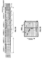
DV Bus 314 to all of thedecoders 316. This technique avoids retransmitting the same tile each time one row of the tile is updated, and retransmitting each update data, but not the complete tile, with the appropriate header and offset display coordinates, e.g., starting and ending row and column to display the update in the relevant display location of the video screen. Similarly, with reference to FIGS. 13A-13C where two users have defined tiles that include some common portions of the same page or record of financial market information, e.g., tile SA and tile SB, the update data for the underlying page or record of financial market information may be transmitted in one of three formats. The first format is to create two separate tiles SA and SB and transmit update data for those tiles as necessary with a duplication of messages. The second and more useful technique is to decompose the overlapping tiles SA and SB into three tiles SA1 which is unique to user A, SB1 which is unique to user B, and SAB which is common to users A and B. Then updates for the three tiles are separately provided as appropriate. A third technique is to create a "supertile" S which includes all of the financial market information. In this latter embodiment, user A is enabled to receive supertile S with display coordinate information for retrieving only those portions of information selected by user A, and user B is similarly enabled to receive supertile S with display coordinate information for retrieving only those portions selected by user B. Thus, the update message is only sent once, yielding improved DV bus messaging efficiency. - 5. Both contiguous-column row messaging and contiguous-row column messaging should be supported within tile messaging for efficient updating of tiles.
-
- The application of tile messaging greatly reduces the amount of message traffic on the
DV bus 314. One example is explained with reference to FIGS. 14A and 14B, which respectively illustratecomposite page 200a having tiles T1, T2, T3 and T4 andcomposite page 200b having tiles T1, T5, T3 and T4', such that tiles T4 and T4' are different user-defined tiles based on the same original portion of financial market information T4*. - First, it is noted that in prior art systems, all vendors of video financial market information typically use contiguous-column row oriented messaging; all screen changes are signaled by multiple individual messages, each message concerning only contiguously located columns in one row of the page or record. A standard page from one commercial vendor may be thought of as one large static alphamosaic tile 250-A that is 80 columns wide and 18 rows high. When the page is transmitted to the client site for the first time in response to a page request by a user, it may be sent using eighteen messages, one for each display row. Each message will include a header identifying the page or record number of the source financial market information, the row number, and the starting column number of the following message, and up to 80 columns of character data. Each message corresponds to a single row and is about 100 characters (one byte per character) in length. Thus, for an 18 row display, the total page requires 1800 characters to be transmitted over the telephone line. At 180 characters per second, it takes about ten seconds to "paint" the screen for the first time.
- When an information change occurs, the information vendor updates the page by sending only the new information. When one character changes, for example, a single message is sent having control information (in brackets) and the new data as follows:
[{PAGE NO}{ROW}{STARTING COLUMN}] DATA
[{P16251}{R0}{C13}]1. Thus, most update messages only represent one or two new data characters to be displayed on the video screen to be displayed on the video screen accompanied by about ten information control "characters" for placing the data characters in the proper display locations. Further, when one fundamental data element changes it often causes a flurry of very small individual messages to update other rows or columns. - With the foregoing in mind, and referring to FIGS. 14A and 14B, if the original portion T4* is defined as an alphamosaic tile 250-A, then, without tile messaging and according to the prior art, receiving a new headline would require transmitting a total of nineteen messages (about 1900 characters); seven messages to
composite page 200a and twelve messages tocomposite page 200b. Seven of the messages transmitted to composite page 200B would be identical to those transmitted to composite 200a except that the row display location would be different to reflect the fact that the headline information is displayed higher oncomposite page 200b than oncomposite page 200a. - However, with tile messaging, receiving a new headline would require transmitting a total of one message (under one thousand characters). Both
composite pages composite pages - If the original portion T4* was defined as a scrolling alphamosaic tile 250-S, then using tile messaging would have resulted in both
composite pages - The third embodiment preferably employs tile messaging of update data using a symbolic signaling technique, which will now be described with reference to FIGS. 11A, 11B, 11C, 11D, 12A, 12B, and 12C. FIG. 11A illustrates a transmission technique similar to that discussed above with reference to FIGS. 3A - 3E. However, for the purposes of clarity, no synchronization signals are shown, and only a single row and single column transmission are shown. The tile row and column starting and ending locations will be transmitted in the manner described elsewhere.
- FIGS. 11A-11C and 12A-12C illustrates message types for alternative techniques of customizing and displaying
composite pages 200 of display information and updating the display information for particular users. With specific reference to a FIG. 11A, one technique uses an enablereception message 100 and data enablesequences sequences reception message 100 is shown as being comprised of display identification (DID) code 120 - reception key (RK) code 106 pairs, in this case, three code pairs DID1/RK1, DID2/RK2 and DID3/RK3. The reception key 106 is used to authorize the decoder to retrieve update data for a portion of financial market information having an IID code that is the same as the reception key. Thus, adecoder video screen 317 having the DID 120 of ID1 is authorized to receive information forreception key 106a RK1, thedecoder video screen 317b with DID 120b of ID2 is authorized to display financial market information for reception key 106b of RK2, and so on. It should be understood that, although the RK's 106 and DID's 120 are illustrated as alphanumeric characters RKn and IDn (n being an integer) in practice it is preferred that they be multibit, e.g., 21 or 24 bits, code words that encrypt the actual source of financial market information. This is so that an unauthorized user cannot identify and retrieve a certain financial market information by tapping into the DV bus. - Following the
enable reception message 100, at time t1 three separate data enable sequences 102-104 are illustrated, each of which is comprised of a reception key 106, row and column display location information 108, followed bydata 110. Although thedata 110 is shown as directly following the reception key 106 and row and column information 108, it can be transmitted on a separate line, immediately following the data enabling sequence. - For the purposes of this example, the information displayed on the respective portions of financial market information having IID codes RK1-RK3 can be different, but each contains at least one common information field of
data 110, which is represented by "DATA1" relating to a 30-year U.S. Treasury bond. By transmitting theinformation field data 110 with the foregoing data enablesequences RKs 106a-106b of RK1-RK3, the threedifferent video screens DIDs 120a-120c of DID1-DID3, can display thesame information field 110 in different locations as illustrated byboxes display coordinates 108a-108c. - For example, the data enable
sequence 102 places thedata 110 in the upper left hand corner represented bydisplay coordinates 108a (ROW1,COL1) ofvideo screen 317a (box 111a) having the DID 120a of DID1, which was enabled with reception key 106a of RK1. In a similar manner, sequence 103 places theinformation field 110 near the center ofvideo screen 317b (box lllb) having the DID 120b DID2, represented by the display coordinates 108b (ROW10,COL40), which was enabled with reception key 120b of RK2.Sequence 104 places theinformation field data 110 toward the lower right hand corner ofvideo screen 317c (box lllc) having the DID 120c of DID3, represented by the display coordinates 108c (ROW3,COL3) which was enabled with the reception key 106c of RK3. - Thus, the
information field data 110 is transmitted by threeseparate tile messages underlying tile 350. In order to customize the information displayed on various displays, separate tiles must be transmitted to eachvideo display 317. When it is necessary to update the financial market information forinformation field data 110 during time interval t2, again three tiles, e.g., illustrated as data enable sequences 112-114, must be transmitted, each having the appropriate reception key 106, row and column 108, and the new financial market information forinformation field data 110, e.g., DATA2, as shown in FIG. 11A. - The application of symbolic signaling is based on the realization that the traders of financial instruments prefer to select the financial market information they use to formulate their trades, and that some of that financial market information will be the same as that used by other traders, and some information will be different. It also is based on the realization that the traders do not necessarily want to view all of the information provided by a commercial information vendor and prefer to customize their video screens to satisfy their desires.
- Accordingly, the customization of the information displayed on multiple decoder video screens is greatly facilitated, and at the same time, the overhead required to update information commonly used is greatly reduced, according to the present invention, in the following manners. Referring to FIG. 11B, one aspect of the present invention provides for using enable reception and initialization messages 116-118 and data enable
sequences 128 at time t1 and 134 at time t2. Each enable reception and initialization message 116-118 respectively includes a DID code 120 for a video screen, an IID code which, in this instance, is used as a secondary reception key (SRK) 122, in this case "LONGBOND", and display coordinate information 108, e.g., row R and column C. The display coordinate information 108 row R and column C will place thedata 110 associated with thesecondary reception key 122 in the designated display location only for the video screen identified in the DID/SRK set. The term "secondary reception key" is a reception key that is associated with another reception key such that a decoder must be enabled with the other first or primary reception key before it can be enabled by a secondary reception key. The other reception key also may be a secondary reception key associated with yet another first or primary reception key as explained below. - Thus, each enable reception and initialization message both enables a video screen to receive and display certain data and initializes the relative display location of that data on that video screen, even though no data has been sent. Importantly, this permits each user to select the display location on the user's video screen to display the data corresponding to the secondary reception key SRK independently of the other users so that only the particular secondary reception key and the corresponding data need be sent to effect the correct display. Again, the use of LONGBOND as an IID code and an SRK is for illustrative purposes and in practice an encrypted multibit bit code word would be used as the SRK.
- Thus, using enable reception and initialization messages 116-118,
video screen 317a having the DID 120a of DID1 is enabled in this example, e.g., at the beginning of the day, withSRK 122 LONGBOND and will display the subsequently transmitteddata 110 information starting at display coordinates 108a (ROW1,COL1). Similarly,video screen 317b having the DID 120b of DID2 is enabled with theSRK 122 LONGBOND and to receive and display thedata 110 information at its selected display coordinates 108b (ROW10,COL10).Video screen 317c having the DID 120c of DID3 will likewise place thedata 110 information at its selected display coordinates 108c (ROW20,COL60). Then, at time t1 a singletile data message 128 is transmitted comprising theSRK 122 LONGBOND and the financialmarket information data 110, shown as DATA1. Upon receiving thetile data message 128,decoder video screen 317a will recognize theSRK 122 LONGBOND as matching its previously enabledSRK 122 and place thedata 110 DATA1 in the designated location according to the previously initializeddisplay coordinates 108a, i.e., the upper left hand corner (ROW1,COL1)box 111a as shown in FIG. 12A;video screen 317b will likewise display thedata 110 DATA1 ofmessage 128 in its center (ROW10,COL40) box lllb, andvideo screen 317c will similarly display thedata 110 DATA1 ofmessage 128 in its lower right hand corner (ROW20,COL60) box lllc. When it is necessary to update the financial market information at time t2, a singletile data message 134, is transmitted, comprising theSRK 122 LONGBOND and thedata 110 DATA2 to update the video screen. Thisdata 110 is then displayed in the proper location of eachvideo screen 317, in the same manner, to update the display. - Referring now to FIG. 11C, another aspect of the invention concerns using three types of messages to display and update information, enable
reception messages 100,initialization messages sequences reception messages 100 are used in the same manner and for the same purpose as described above in connection with FIG. 11A. Then, once a decoder is enabled with a reception key 106, the enabled decoder is initialized with a secondaryreception key SRK 122 for that enabled reception key 106, and display coordinates 108 for displaying the subsequently transmitteddata 110 in the selected display location 111 on avideo screen 317. Thus, eachinitialization message video screen 317. Then, at times t1 and t2, thedata messages 128 and 132 described above in connection with FIG. 11B are transmitted, having theSRK codes 122 LONGBOND, which will be received by the enabled and initialized decoders, and thedata 110 for display at the indicateddisplay locations respective video screens - The initializing
messages reception messages 100. Thus, if the decoder is not first enabled with the reception key 106 by anenable reception message 100, it will not retrieve thesecondary reception key 122 by an initialization message and will not retrieve thedata 110 from a data enable sequence of thetype - A comparison of the information that must be transmitted using the scheme of FIG. 11A, at time t2, with that of FIGS. 11B or 11C at time t2 readily demonstrates the reduction in message transmission overhead produced using either symbolic signaling scheme in accordance with this form of the present invention. Also, the techniques illustrated in FIGS. 11B and 11C enhance the flexibility for producing user-customized displays in accordance with particular client requests while reducing the volume of data enable sequences to display and update financial market information.
- In this regard, the user who is enabled with a reception key may select locally a new location for a tile of financial market information selected from the enabled financial market information. To do so, the user would select the tile using the
keyboard 319 or a mouse 319', and define an offset of the selected information by moving the tile to its new display location on the video screen, relative to either the origin of the underlying source portion of the financial market information or to the origin of the default tile location. This new tile position information is communicated overcontrol bus 318 to host CPU 425 (see FIG. 11) which may generate a new initialization message with the SRK for the tile (i.e., an information identification code) and new display coordinates. Thereafter, any update data for that tile will be mapped from the position of the update data relative to the default origin onto the user-defined tile and displayed (to the extent the update data occurs in the user-defined tile). - The user may relocate the tile to a different position on the display screen. This change also will be either followed by an initialization message so that any update data falling within the first defined tile is mapped into the new display location, which remains the same with respect to the display location relative to the original page or is remembered so that any update data falling within the first defined tile is mapped into the new display location by the decoder, e.g., by adjusting the display coordinates as the update data are stored.
- The use of secondary reception keys provides a convenient technique to minimize message overload. Moving a tile defined by an enabled secondary reception key and initial (or default) display coordinates, has the effect of changing the display coordinates so that the data corresponding to the secondary reception key will be mapped into the tile in its new location. Thus, the user may easily customize the provided data for commonly used data by using secondary reception keys and initializing the display coordinated for the financial market information.
- Referring now to FIG. 11D, an embodiment of a
decoder 316 employing symbolic signaling operates in the following manner. The following definitions are used. DID is a unique decoder identification code; DIDR is a DID code in a message received by a given decoder; DIDO is the unique DID code stored in a given decoder; RK is a reception key; RKR is the first reception key in a message received by a decoder; RKN is a reception key in a message received by a decoder that was not previously stored in the decoder; RKO is a reception key that was previously stored in the decoder; R# is a start row number; C# is a start column number; and D is a string of data to be displayed. - There are at least seven types of messages, wherein the brackets contain the identified fields of the message as follows:
- Enable Reception Messages
[DID, RKN]
[DID, RKN, R#, C#] - Initialization Messages
[RKO, R#, C#]
[RKO, RKN]
[RKO, RKN, R#, C#] - Data Enable Sequence
[RKO, D]
[RKO, R#, C#, D] -
- The enable reception message that associates a DID and an RKN provides the decoder having a DIDO matching the DIDR code in the message with a new reception key RKN, which is stored and thus becomes an RKO as to subsequent messages. The decoder may store one or more RKOs at any given time.
- The enable reception message that associates a DID, an RKN and an R# and C# provides the decoder having a DIDO matching the DIDR in the message with a new reception key RKN and display coordinate information (R#, C#) for that RKN. The display coordinates are relative to the video screen origin (on the underlying tile). The decoder can store many different RKOs and their corresponding display coordinates intended for display on any particular video screen. Each enable reception message will be ignored by any decoder not having a DIDO matching the DIDR in the received message.
- The initialization message that associates an RKO and display coordinate information R# and C# will provide the new display coordinate information for the already stored reception key RKO for each decoder that was previously enabled with that reception key RKO. The display coordinate information defines the offset of RKO relative to the video screen origin (on the underlying tile).
- The initialization message that associates an RKO and an RKN will enable each decoder that was previously enabled with RKO with an additional new reception key RKN in the received message for the same portion of display information.
- The initialization message that associates an RKO, RKN and R# and C# enables each decoder previously enabled with reception key RKO with an additional new reception key RKN and display coordinate information (R#, C#). The display coordinate information defines an offset for the reception key RKN relative to the video screen origin (on the underlying tile).
- Each initialization message will be ignored by a decoder that was not previously enabled with the reception key (RKO) that matches the reception key RKR in the received message.
- The data enable sequence that associates an RKO and data D is provided to each decoder and the data is retrieved by each decoder that was previously enabled with the identified RKO and is ignored by the other decoders. If no display coordinate information R#, C# has been stored in the decoder for the identified reception key RKO in the received message, then the decoder will store and display the data D without an offset relative to the stored origin of the tile corresponding to RKO; when there is associated display coordinate information stored it will be used.
- The data enable sequence that associates an RKO, data D to be updated and display coordinate information R#, C# is provided to each decoder and is retrieved by each decoder that was previously enabled with the identified RKO and is ignored by the other decoders. The data D is stored and displayed using the provided display offset information (R#, C#). Thus, the data is displayed at a location offset by R# and C# relative to either the video screen origin (if no previous RKO offset was stored in the decoder) or the data is displayed offset by R# and C# relative to the previously stored offset of RKO.
- Referring still to FIG. 11D, a flow chart for symbolic signaling, from the perspective of messages received at the decoder, will now be discussed. The processing routine is entered at
node 1200, and it passes to step 1202, which tests for a received message. When no message is received, the decoder system returns tonode 1200 and waits for a message. When a message is received, the routine proceeds to step 1204 where the message is evaluated first to determine if the first reception key RKR in the message is a received code DIDR that matches the unique DIDO (typically a code stored in a ROM device in the decoder). Upon a match the system moves to step 1206 where the second received reception key RKR in that message is considered a new reception key RKN and is stored in the decoder. That RKN thus becomes a stored reception key RKO as to any subsequently received message. - Following storage of a reception key at
step 1206, the routine advances to step 1208, which determines whether the message contains row R# and column C# information associated with the received and just stored reception key. If offset information is present, the associated display coordinate information R#, C# is stored instep 1210, and defines the offset for that received and stored reception key RKN. The offset is defined relative to the origin of the underlying tile. Following storage of the information, the system returns tonode 1200 for the next message. If there is no display coordinate information in the message, then the system returns tonode 1200 for the next message. - If at
step 1204 it is determined that the first reception key RKR in the message does not match the DIDO code, then the routine moves to step 1212 and the message is evaluated to determine whether the first received reception key RKR matches a previously stored reception key RKO for the decoder. If it does not, then the routine returns tonode 1200 and waits for the next message. If it does, then the routine proceeds to step 1214 where the message is evaluated to determine if it also contains a new second reception key RKN. - If a new reception key RKN is present, then the routine proceeds to step 1216 and the new second reception key RKN is stored, and thus becomes a stored reception key RKO as to any subsequently received message. After storage of a new reception key, the routine next proceeds to step 1218 where the message is evaluated to determine if it contains display coordinate information R#, C#.
- If new display coordinate information R#, C# is present at
step 1218, the offset location information for RKN is stored atstep 1220. If the message does not contain a new reception key RKN as determined atstep 1214, then the routine passes to step 1226 where the message is evaluated to determine if new display coordinate information R#, C# is present. If it is, it is stored atstep 1228 to define the offset for the data associated with the reception key RKO. - If the message does not contain display coordinate information, or after any such information is stored, the routine passes to step 1222 where the message is evaluated to determine if any data is present. If no data D is present, then the routine returns to
node 1200 and waits for another message. If data D is present, then it is stored and displayed using the display coordinate information most recently associated with the stored reception key RKO matching the received reception key RKR in the message atstep 1212. Thereafter, the routine returns tonode 1200 and waits for the next message. - It is noted that the symbolic signaling routine may be combined with the nonsymbolic signaling techniques described above. It also is noted that other enabling, initialization and data messages and complementary messages for disabling reception and/or removing reception keys and display coordinate information can be created, sent, and processed in a similar manner.
- According to the present invention, the encoder stores a
composite page 200 as a number of tile definitions and messages. This allows the system to store, transmit, and/or display information in an efficient manner using a technique referred to as cellular micrographics. Cellular micrographics is described with reference to FIG. 15, Tables I and II, and an illustrative cellular micrographics transmission algorithm, using two (one foreground/one background) colors per pixel wherein: allcells 210 in an alphamosaic tile 250-A are transmitted as extended ASCII characters, i.e., each character is represented by one byte of data and there is one character percell 210; cells of a graphic tile 250-G are transmitted as one or more bits per pixel and, hence, multiple bytes of data percell 210; graphic tiles 250-G may contain both graphic cells (multiple bytes of data per cell) and alphamosaic cells (a single byte of data per cell); and, for the sake of processing efficiency, each tile 250 (except video tiles 250-V) may run-length encode the signals (either horizontally or vertically) prior to transmission. - FIG. 15 shows a graphic tile 251-G that has ten cell rows and ten cell columns and is described in Table I, where b=blank character per cell, a=one ASCII character per cell, and p=pixel defined cell.
Cell Row Contents Notation R0 10 blank characters 10b R1 10 ASCII characters 10a R2 10 blank characters 10b R3 5 blank characters, 3 pixel defined cells, 2 blank characters 5b,3p, 2b R4 3 blank characters, 3 pixel defined cells, 4 blank characters 3b,3p, 4b R5 2 blank characters, 2 pixel defined cells, 6 blank characters 2b,2p, 6b R6 2 blank characters, 1 pixel defined cell, 7 blank characters 2b,1p, 7b R7 1 blank character, 2 pixel defined cells, 7 blank characters 1b,20, 7b R8 10 blank characters 10b R9 10 blank characters 10b - Because the cellular micrographic algorithm preferably uses run length encoding and cell wrapping within the tile 251-G, the tile 251-G can be completely defined by the messages described in Table II. The calculations in Table II assume that single-bit-per-pixel signaling is being used and that each pixel-defined
cell 210 is individually specified by 16 bytes of data (sixteen rows of eight columns of single bit values).Message number Representing Length [in bytes] 1 11b 1 [1] 2 8a 9 [1 + 8] 3 16b 1 [1] 4 3p 49 [1 + 3(16)] 5 5b 1 [1] 6 3p 49 [1 + 3(16)] 7 6b 1 [1] 8 2p 33 [1 + 2(16)] 9 8b 1 [1] 10 1p 17 [1 + 1(16)] 11 8b 1 [1] 12 2p 33 [1 + 2(16)] 13 27b 2 [1 + 1] TOTALS: 100 cells 198 bytes - Thus, by using the cellular micrographics technique of the present invention, the amount of required transmitted data to display the tile 251-G is reduced by a factor of approximately eight from 1,600 bytes to 198 bytes. The 1,600 bytes is based on 16 bytes per cell and 100 cells.
- The 198 bytes represent 13 control bytes, 8 ASCII characters, 11 pixel cells (16 bytes each), and 1 blank, or:
- Still greater efficiencies may be accomplished by using run length encoding within pixel defined cells.
- Referring to FIGS. 11, 16, and 25-27, a DV bus signal structure and signaling method, between the
encoder 312 and a plurality ofdecoders 316 and/ordesk interface units 321, in accordance with a preferred embodiment of the invention, is shown. Theencoder 312 includes areceiver 510 for receiving input messages from a host central processing unit (CPU) 425 and a residual video converter (RVC) 400. These messages are then applied to an error detection and correction (EDAC)circuit 520, which adds parity and interleaving to protect against both single and burst errors. The output of theEDAC circuit 520 is passed tomodulation circuit 530, which functions to increase the data throughput rate and facilitate subsequent signal processing and clock recovery in each decoder. References to a decoder should be understood to includedesk interface units 321 where the context permits. -
Modulation circuit 530 converts the binary digital data into a quad level (8,9) modulated signal, as described below. The output of themodulation circuit 530 is passed to the multiplexor (MUX)circuit 540 which switches between, on the one hand, the digital data fromCPU 425 and video data fromRVC 400 and on the other hand time-compressed television program information signals which are received from television feed converter (TFC) 450.MUX circuit 540 drives the output ofencoder 312 ontoDV bus 314. - Each decoder 316 (only one is discussed for the sake of convenience) includes an analog front-end signal processor (AFESP)
circuit 610, which receives the DV bus signals, recovers a clock signal from the modulated signal and establishes detection thresholds for processing the quad level DV bus signals. The output ofAFESP circuit 610 is passed to demultiplexor (DEMUX)circuit 620, which demultiplexes the television program information signals and the digital-video signals, such that each may be further processed and provided tovideo screen 317.DEMUX circuit 620 passes the digital-video signals todemodulator circuit 630 which converts the quad level (8,9) modulated signals into binary signals. - The output of
demodulator circuit 630 is passed to error detection and correction (EDAC)circuitry 640, which uses and then removes the parity bits to output digital signals that correspond to the signals input toencoder EDAC circuit 520 as a best estimate of the intended message. The message is then transmitted tocircuit 650, which checks the syntax of the message and stores the display information in the designated address locations of a picture store memory. - The television program information signals separated from the DV bus message by
DEMUX circuit 620 are separately passed tocircuit 670 which converts the compressed television program information signal into displayable television image signals, and then provides those image signals to switch 680.Switch 680 selects between passing the television image signals and the digital display information tovideo screen 317. - As illustrated in FIG. 17, signals transmitted on
DV bus 314 are transmitted in packets t. If no television program information signals are to be transmitted on the system, the packet t may have a time length that is variable, according to the amount of data in each message. If television program information signals are to be transmitted, then the packet t has a fixed and uniform time length corresponding to time length of the television standard video scan line. Thus, for NTSC television, the packet t time block is about 63.5 microseconds. - Each packet t includes a digital display information packet d including a header portion H, a data portion D and a parity portion P. The header H contains information that allows each
decoder 316 to identify the beginning of a packet t, and to detect digital signal transitions to compensate for the transmission loss characteristics of the communication channel. The parity bits P are collectively illustrated as following the data D in FIG. 17, but in practice may be interspersed among the data D according to conventional parity and interleaving error detection and correction coding techniques. - The digital packets d carry all the display information except television program information signals. One or more digital packets d constitute a DV bus "message" used by each
decoder 316 to modify the displayed screen image. - Each packet t also may include a television (signal) packet v, including one or more realtime television program signals illustrated as "TV". Signals for different television images are given different letters, such that TVA, TVB, and TVC represent three different television display images. The
subscript numbers - The digital packet d of each packet t may vary from one time length tn to the next tn+1, depending on the amount of data D and television video information TV that is to be transmitted in each packet t. To reduce the amount of memory required in each
decoder 316 that is equipped to receive a realtime television program information signal, it is useful to signal an amount of information necessary to generate about one TV scan line within the time period t of one TV line. With reference to FIG. 17, this means that the second TVB line TVB2 must occur no later than 63.5 microseconds after the first TVB line TVB1. This does not however, require that the consecutive TVB line signals be uniformly or periodically spaced. - Typically, DV bus messages are not sent to a
decoder 316 faster than thedecoder 316 can buffer and act upon them. Because theDV bus 314 is a simplex transmission channel, theencoder 312 must keep track of the messages being sent to eachdecoder 316 and the time required to execute each message. Subsequent messages are queued until all of thedecoders 316 that have to receive and act upon a given message are able to do so. - Referring to FIGS. 16 and 18-19,
modulation circuit 530 anddemodulation circuit 630 are complementary for the selected modulation protocol. There are four considerations for selecting a signal modulation method: (1) clock recovery, (2) start of message identification, (3) information transmission rate, and (4) bit error rate. Alldecoders 316 must recover a digital clock from the received DV bus signal. Therefore, the transmitted DV bus signal must have an adequate number of digital transitions for this purpose, regardless of data D content. Further, thedecoder 316 must be able to determine the start of the message in a reliable manner. - In the present invention, a quad level digital signal, transmitting two bits of information every signaling interval SI is used as a reasonable engineering trade-off between data throughput and bit error rate. Since each signaling interval SI carries exactly two bits of information, it is also referred to as a "dibit" interval. An (8,9) interval modulation method is implemented to transfer one word (16 bits) of demodulated data D to the
decoder EDAC 640 at a time. The structure of this modulation method is illustrated in FIG. 18, wherein SI is the signaling interval and MI is the modulation interval. The rule for determining the signaling level of the modulation interval MI is to maximize the transition occurring at the leading edge of the modulation interval MI. That is, if the signal level in the signaling interval SI just before the modulation interval MI islevel level 0. If the signal level in the signaling interval SI just before the modulation interval MI islevel level 3. - Referring to FIG. 19, the header field H is 50 signaling intervals SI long and includes six subfields. These subfields provide information to each decoder for the decoder to recover the clock signal and compensate for the transmission characteristics of the
DV bus 314 and any interconnections. - Subfield one has a length of 9 signaling intervals and contains eight dibits of the maximum value signal. This is followed by subfield two, which also is 9 signaling intervals long and which contains eight dibits of the minimum value signal. These two subfields intentionally violate the modulation rule and set the maximum and minimum input signal range to allow the
decoder 316 to detect the start of a packet d and fine-tune its decision thresholds to compensate for attenuated received-signal levels, and may be used to signal the possibility of the beginning of a header field H. However, the start of a data decision will only be made after all six subfields are properly received. - Subfields three, four, and five each have a length of 8 signaling intervals and may be used to fine-tune decision thresholds to discriminate between signals at
levels levels levels - Subfield six has a length of 8 signaling intervals SI and is used as a delay and clock run-in prior to the start of data field D. It is also used to specify the interleaving depth for Error Detection and Correction (EDAC) as explained next.
- Referring to FIGS. 16 and 19, the
encoder EDAC circuit 520 adds parity bits to the message. This permits thedecoder 316 to detect and correct the errors that occur during signal transmission. Parity both increases the reliability of the messaging, as evidenced by a decreased bit error rate, at the expense of decreasing the message data throughput. - Development efforts indicated that an error detection (e.g., checksum) and replication correction method would likely be inadequate. It was discovered that system performance was improved by using a single error correcting and double error detecting code (e.g., Hamming) within a single level interleaving framework. While non-interleaved burst error correcting codes exist (e.g., Reed-Solomon), their implementation was believed to be more difficult in an ASIC environment in which the present invention is preferably implemented.
- Referring to FIG. 20, digital data D to be transmitted is written bit by bit horizontally into a double buffer. When the first row of data is filled, data is written into the next row and the parity bits P corresponding to the data D in the first row are calculated according to the EDAC methodology rule selected. This process continues until the entire buffer is filled. The buffer is then locked to prevent further input, and transmitted to the
modulator circuit 530 bit by bit vertically. The buffer may be reused after its entire contents have been transmitted; double buffering sustains continuous message output from theencoder 312. - Each buffer row includes both data D and parity P, and represents one codeword. Assuming that a single error correcting double error detecting code has been used, without interleaving the following errors illustrated in FIG. 20 have the results indicated in Table III:
Error Codeword errors Action A,J,K,L Single in data field Correctable B Single in parity field Correctable C,Z Double in data field Detectable, not correctable E,F Double Detectable, not correctable G,H,I Triple Not detectable, may not give error - The nature of the
digital video bus 314 is that errors occur in bursts. Apart from randomly-occurring single bit errors, the probability of a second error immediately following the first error is relatively high. For example, if the probability of a first error is 10-9, the probability of the next bit being in error is not 10-9 but might be 0.9, and the probability of the following bit being in error might be 0.8. Therefore, a single-correcting methodology is ineffective in this type of transmission channel. Interleaving, i.e., buffering the data to be messaged horizontally and transmitting it vertically, causes burst errors to be spread among several codewords. In this regard, a burst error J,K, and L of length three in the channel is mapped into three single codeword errors and this is correctable by the chosen error detection and correction scheme. - By choosing a large interleaving depth of n codewords, e.g., 32 codewords, it is possible to protect against relatively long burst errors with a relatively simple single error correcting code. For example, when using an interleaving depth n of 32, a burst error of up to 32 bits is fully correctable, all errors of
length 33 to 64 are detectable, and all those with greater length could possibly result in errors. The occurrence of single bit errors plus burst errors will degrade the performance of the system in a manner determined by their location. - The maximum possible interleaving depth depends on both the maximum buffer size and the number of TV signals to be transmitted. This is because each time-compressed TV signal must occupy a time slot occurring once a line time, i.e., in successive packets t. Therefore, the maximum length of digital packet d is determined by both the television program information signal compression factor and the number of TV signals being transmitted simultaneously. Preferably, the interleaving depth n should be maximized within the time constraints imposed by the number of TV signals being transmitted. Thus, with reference to FIG. 7A, the possible interleaving depth n between lines U and W and between lines X and Y are the same, and is greater than the interleaving depth m between lines W and X and between lines Z and V. This is because the latter two series of DV bus signals also include TV lines for television program information signals TV2 and TV3. Accordingly, the interleaving depth n will change with the amount of television program information signals being transmitted.
- Referring to FIGS. 21-23, a plurality of digital video bus messages are now described. The messages are controlled in two layers, a transport layer, for detecting and receiving data sent to a
specific decoder 316, and a message layer, for executing application firmware or software. Processing is done by a custom Packet Reception Application-Specific Integrated Circuit (ASIC) including a microprocessor located in thereceiver module 610 of thespecific decoder 316. TheASIC module 610 may have any structural implementation so long as it performs the signal processing functions described and illustrated. Configuration of an ASIC is within the ability of a person of ordinary skill in the art. - Regarding the transport layer, referring to FIG. 21, the transmission of variable length packets d are concatenated to form complete messages in the presence of time multiplexed television program information signals (e.g., TVA and TVB), are shown. The message format is summarized in Table IV below:
Message (M) Packet (t) Interleaving Depth 1 1 D0 2 D1 3 D1 4 D2 2 1 D2 2 D2 3 1 D1 2 D1 3 D0 4 1 D1 2 D1 3 D2 message 1, designated M1-P4 in FIG. 21, has an interleaving depth of D2 corresponding to the time used by the two TV signals. - Referring to FIG. 22, the location of the digital packet d fields are illustrated.
Field 0 contains a message header.Field 1 contains the end of message (EOM) flag which indicates that the current packet d is the last one in the current message when the EOM flag is set. This enables the hardware to process the reception keys contained infields -
Fields Field 2 contains the "address type" which is used to specify the meaning and use of the contents in the address (Field 3). In a preferred embodiment, the address type field contains two bits. A value of 00 indicates that the following address field contains a unique display identification code for a given a decoder video screen, i.e., a DIDO. If the address field value is 01, then the address field contains a new to be stored information identification code for atile 250, i.e., an RKN. If the address field is 10, then the address field contains a previously stored information identification code for atile 250, i.e., an RKO. If the address field value is 11, then the address field contains a packet sequence number (PSN), having a value of from 1 to 31, and thedecoder 316 checks for sequential numbering of packets d within the message. An out-of-sequence number causes the entire message to be rejected. -
Field 3 is the "address field" and may have up to 21 bits. Accordingly, there may be up to 221 = 2,097,152 different unique identification codes for each address type, i.e., video screens and pages, records, portions and tiles of display information. -
Field 4 has sixteen bits and provides the "message length" which is only transmitted in the first packet d of a message. It indicates the total length of the message in bytes. -
Field 5 contains the data D used to form the display information message. It has a variable bit length. - Regarding the message layer of the
DV bus 314, there are two classes of messages that can be accommodated, supervisory messages and image data messages. Supervisory messages direct one or more decoders to perform control and/or bookkeeping actions, such as enabling a reception key or defining a tile. Image data messages refresh or update the contents of a displayed tile. Such messages always cause thedecoder video screen 317 to update even if the display information is unchanged. - All received packets d are concatenated into messages at the
decoder 316. The location of the received message fields is illustrated in FIG. 23.Field 0 is the reception key (RK) and contains 3 bytes.Bit 0 is set to 0,bits 1 & 2 contain address type and bits 3-23 contain the address (cf. FIG. 22).Field 1 contains the "message length"; it uses two bytes to specify the length of the message in bytes. -
Field 2 is the "message sequence number" and is a one byte field. It contains a message sequence number for messages to the reception key RK specified inField 0. Thedecoder 316 verifies that the difference between the current and last received message sequence number is always one modulo 256 to ensure that all messages to the current reception key RK are received in order. When an out of sequence number is detected, an error request is transmitted by thedecoder 316 over the control bus 318 (See FIG. 11) indicating the last correctly received message. -
Field 3 is the "Command" field, and has one byte which indicates the operation to be performed on the contents of the data in followingField 4, the variable length part of the message. A Command may be self acting, i.e., the data field contents immediately following is null. The byte length of the data inField 4 is limited by the time length t of each message and the video signals v in each message. - In a preferred embodiment, the
message Command field 3 has the following commands anddata Field 4 has the following associated data: Amessage Command byte 0 initializes decoder hardware and clears the video screen. There is no associated data. Amessage Command byte 1 sets the parameters to configure the video screen hardware and software. Associated data bytes 0-7 contain the ON and OFF period for four blink counters, and data bytes 8-11 contain the motion period for four motion counters. Amessage Command byte 2 operates to clear the video screen, making all pixels the background color. There is no associated data. Amessage Command byte 3 operates enable reception. It instructs the uniquely identifieddecoder 316 to enable reception for the specified reception key, and associates this reception key with the request string for thespecific tile 250 sent by thedecoder 316 to thehost CPU 425 via thecontrol bus 318. For this message Command, the associated data is, for bytes 0-2, the tile reception key, and for bytes 3-23, the tile request string. Amessage Command byte 4 sets the tile definition. It defines thetile 250 whose number is specified in theaddress Field 3. The first associated data byte specifies the default color index for the portion of display information. The second data byte specifies the default display attribute. The third data byte represents the number of symbolic tile definitions (the number of 11 byte packets following). Each of these definitions contains a 16 bit symbol number (tile IID or RK), the two corner display coordinates (upper left and lower right; a rectangular tile boundary is assumed), the default symbolic tile attributes and the value of the motion counter if the tile is a panning or scrolling tile. The associated data bytes are:byte 0default color index byte 1 default display attribute byte 2-3 default upper left row and column number byte 4-5 default lower right row and column number byte 6 tile motion attribute byte 7 current motion index byte 8 default character table byte 9 number of text messages composing the tile byte 10 current message sequence number(s) for tile messages 1 to n - A
message Command byte 5 sets the color table. It contains a number (specified in data byte 0) of definitions for the color table. Each definition contains four bytes. The first data byte is an index (0-255) into a color table. The three other data bytes represent background color, foreground color and line color respectively. Each of these three data bytes is encoded internally as IIRRGGBB: two bits to define the overall INTENSITY (I), two bits to define the RED (R) intensity, two bits for the GREEN (G) and two bits for the BLUE (B). The associated data bytes are:byte 0number of color definitions byte 1 new color index byte 2-4 background, foreground, line colors byte 5-8 next color definition (same as bytes 1-4) byte 9-12 next color definition (same as bytes 1-4) - A
message Command byte 6 operates to send new text to the video screen. The characters contained in the data section are put on the screen in contiguous columns or rows, depending on the axis of consecutiveness, using cell wrapping. The associated data bytes are:byte 0message id (Tile-relative) byte 1message sequence number byte 2 relative row number byte 3 relative column number byte 4 number of data bytes following byte 5... data in TEXT format - A
message Command byte 7 provides for downloading programming code into thedecoder 316 application program memory. The associated data bytes are:byte 0program revision code byte 1-4 section address byte 5 last section flag byte 6... program code - A
message Command byte 8 clears a tile. It causes all pixels in the tile to be set to the default background color. There is no associated data. Amessage Command byte 9 is a "Genlock", which is functionally equivalent to a vertical sync pulse in a video signal. There is no associated data. Amessage Command byte 10 is to define a character set. It downloads a pixel map for a character set for converting a one character byte to a multibyte pixel representation. The associated data bytes are:byte 0Character table ID byte 1 Starting character code byte 2 Number of codes defined byte 3...Bit map definitions (16 bytes each) - When a
tile 250 is defined in theencoder 312, a static array of messages is allocated to, and associated with, thattile 250. All messages in theencoder 312 are kept in a queue and are sent out, in their entirety, in a message cycle whose period varies according to system scheduling constraints. - The system is preferably tuned to optimize message scheduling for its particular mix of static alphamosaic tiles 250-A, graphic tiles 350-G, motion tiles 350-P, 350-S, RVC tiles 350-V, TFC "tiles" 350-V, and the number of decoders and video screens. One suitable message prioritizing schedule is the following order: individual decoder directed messages, scheduled messages (tile motion control), tile update data messages, decoder re-requested tile update messages, alphamosaic refresh messages, administrative messages, and graphics refresh messages.
- The message layer protocol supports three kinds of attributes for cells 210: motion, cell and color. The motion attribute is an eight bit word that is encoded MOV, C1, C0, V, NU, NU, NU, NU, where MOV, C1, C0, V are movement,
movement control byte 1, movement control byte O, video and NU stands for unused bits. The cell attribute is an eight bit word and it combines both software and hardware attributes. The byte is encoded REV, ULIN, NU, NU BR1, BR0 BE1, BE0 where BR1, BR0, BE1, BE0 areblink rate 1,blink rate 0, blinkeffect 1, blinkeffect 0, REV stands for reverse video and ULIN stands for underline. These last two attributes are implemented in software and therefore need not reside in the character cell. The color attribute is an index into the color table. - The message layer protocol uses a byte oriented TEXT format to specify control, alphanumeric text, and graphics. The lowest nine bytes are control bytes and have the following special meanings:
Byte 0 specifies that the next byte will contain a repetition factor for run length encoding to specify how many times the cell definition that follows should be repeated along the axis of consecutiveness.Byte 1 specifies that the next 2 bytes will contain the relative row and column number applicable to the following text.Byte 2 specifies that the next 16 bytes define a graphic cell to be put in current location.Byte 3 specifies that the next byte is to become the current cell attribute, meaning that it will apply to every subsequent cell defined in the message.Byte 4 specifies that the next byte contains the size of the cell specifications to come. The sizes allowed are 0 for normal size, 1 for double size, 2 for triple size and 3 for quadruple size.Byte 5 specifies that the next byte is to become the current color index, meaning that it will apply to every subsequent cell defined in the message. It is not used for graphic cells.Byte 6 specifies that the following cell specifications should be put in consecutive locations horizontally. In other words, to define the address of the next cell, the current column number should be incremented.Byte 7 specifies that the following cell specifications should be put in consecutive locations vertically. In other words, to define the address of the next cell, the current row number should be incremented.Byte 8 specifies that the current cell location is not to be modified, e.g., if the cell contains a character that is defined on another line. For example, if theline 1 contains triple size characters, it also will useline line Byte 9 specifies that the next byte identifies the character table from which the following characters will be drawn. The new character set remains in effect until another change character set command, or the end of message. Bytes OAH-OFH are not used and bytes 20H-FFH are normal cell representations. Printable ASCII character codes are preferably used wherever possible. - The following illustrates how the overall messaging efficiency and system throughput, in accordance with this third embodiment of the invention, may be calculated.
- Consider a system in which signal bandwidth is 22.5 MHz, the packet time length t (including the header H) is 63.5 µs, the error detection and correction code is a 24/30 Hamming code, interleaving efficiency is 100%, modulation is quad level (8,9), and packet efficiency is 100%.
- The signaling interval SI may be determined from the system bandwidth as follows:
- a) the signal edge rise time (tr) should be less than or equal to one-third of the signaling interval SI, and
- b) the bandwidth of the signal (fb) is related to the
signal edge rise time by:
-
- Hence, the minimum signal interval corresponding to a 22.5 MHz bandwidth is:
- The signaling interval is therefore chosen to be:
- Regarding information throughput, since quad level modulation is chosen, two bits are transported in every signaling interval. The capacity of the channel is therefore:
- This capacity is not actually attained because first, every packet starts with a 50 SI header, every ninth SI after the header contains no information ((8,9) modulation is used to aid clock recovery), and the EDAC circuits appends six parity bits to every twenty four data bits (a (24,30) Hamming code is used).
- Second, each packet maximally lasts 63.5 µs. Thus, there can be a maximum of (63,500ns/50ns) = 1,270 SI per packet. The 50 SI header therefore reduces the capacity by a factor of (1270 - 50)/ 1,270 = 96.1%. The modulation efficiency is (8/9) = 88.8% and the EDAC efficiency is (24/30)= 80%. Therefore, the overall efficiency of the DV bus signaling is approximately = 0.961 x 0.888 x 0.800 = 68.27%. This results in an effective DV bus capacity of:
- In practice the
DV bus 314 should be transporting information at a rate of about 20 Mbits/sec or more, which is more than twenty (20x) times that of conventional Ethernet systems. It should be noted that Ethernet has a 10 Mbits/sec capacity of which perhaps only 1 Mbits/sec is realized after protocol and/or error processing. - Referring now to FIGS. 11 and 26,
control bus 318 controls bi-directional communication between a decoder 316 (or a desk interface unit 321) and the system.Host CPU 425 may issue messages targeted to a specific decoder or to all decoders, or may request information from a specific decoder. A decoder will send a message to thehost CPU 425 when requested by thehost CPU 425. - Typical uses of the
control bus 318 from thehost CPU 425 todecoders 316 are to poll adecoder 316 for a message, install anew decoder 316 on the system, update an LED display of akeyboard 319 at adecoder 316 and maintain the control bus protocol. Typical uses of thecontrol bus 318 from thedecoder 316 tohost CPU 425 are to transmit keyboard and/or mouse data (i.e., user requests for display information, or to define or move tiles), report decoder malfunctions, and request system resources, e.g.,DV bus 314 message retransmission due to a detected error in message sequences. - The structure of
control bus 318 is modeled after conventional industry-standard shared bus models. A preferred protocol is one similar to an HDLC unbalanced configuration in normal response mode. Apreferred control bus 318 is a system-wide multi-drop RS-422 or 485 network, where thehost CPU 425 serves as the primary station and up to 63decoders 316 are connected as secondary stations to each RS-422 or 485 strand. Bi-directional communication between eachdecoder 316 and thehost CPU 425 is controlled by a preselected polling scheme emitted by thehost CPU 425. - At installation, the
host CPU 425 assigns a unique control bus address to each decoder. This address consists of a strand ID, which identifies the RS-422 or 485 line to which the decoder is connected, and a 5-bit polling ID. The polling scheme allows thehost CPU 425 to poll each decoder using a single byte, thus making the most frequently used signal the shortest length. - In addition, the
host CPU 425 sends commands to aspecific decoder 316 using its unique 21-bit decoder ID. Unless there are any errors detected, everydecoder 316 along a strand is polled before any decoder is polled a second time. This polling sequence represents a polling cycle. The suitable nominal polling frequency of .2 second, that is, an outstanding message at a decoder will wait not longer than .2 second before it is solicited by thehost CPU 425. The baud rate (nominally 9600 baud) is configurable, depending on the number of decoders in the system. This means that smaller systems may be able to realize a savings by using fewer communications controllers. It also means that systems are easily upgradeable, since the system's control bus capacity can be increased by adding communications controllers. Where desk interface units are used,CPU 425 assigns a polling ID for eachvideo screen 317 and polling and command messages are sent for eachvideo screen 317 on the system, rather than to eachdecoder 316. - Messages between the
host CPU 425 and eachdecoder 316 are in the form of a transaction. All transactions are initiated by thehost CPU 425 and take place between thehost CPU 425 and a single decoder. Referring to FIGS. 24A and 24E, thehost CPU 425 begins its signal by sending a probe message (if it has no command for the decoder 316) or a command message (if it has a command outstanding for the decoder) to a specific decoder. Alternately, thehost CPU 425 may send a "Broadcast" message to all decoders on thatcontrol bus strand 318. Broadcast messages serve a number of purposes (e.g., transmission failure, system-wide keyboard messages, changing communication parameters, etc.). Both command and Broadcast messages consist of a Header, a sequence element (Seq), and one or more requests (R-Frame). - Referring to FIG. 24B, each decoder responds to a
host CPU 425 signal with either a solicitation message or, if no solicitation is ready, an idle message. Idle messages consist of a Seq element only (message bit = 0). Solicitation messages consist of a Seq element (message bit = 1), a poll element, and one or more request frames. A request frame (R-Frame) contains one or more requests from either thehost CPU 425 or thedecoder 316. No more than 64 requests can be sent in one R-Frame. FIG. 24C shows the structure of an R-Frame and FIG. 24D shows the structure of a single request. - Of the three message classes generated by the
host CPU 425, two (Probe and Command) constitute signals. The decoder must respond within a configurable response interval (nominally set at 5 character times), otherwise thehost CPU 425 regards this as a failed transaction. If the number of failed transactions passes a configurable disconnect threshold (nominally set at 5), thehost CPU 425 logically disconnects the decoder from the network and displays a suitable message to the system administrator. - The signaled decoder responds to each host CPU signal with a solicitation or idle message. The value of the AK bit in the Seq element (see FIG. 24G and the discussion below) reflects the reception status of the signal. If the signal was a Probe or a successfully received Command, the AK bit is 1. If the signal was a Command, and the R-Frame was not received successfully, the AK bit is 0.
- The decoder regards the transaction as successful if the next message sent by the host is a signal to another decoder. Otherwise, a negative acknowledgement is assumed. If the next host message is another signal to this decoder, it retransmits the solicitation. On an error, the
host CPU 425 will re-signal a decoder up to a configurable number of times (nominally 5), and then send a broadcast message. This indicates a communication failure without providing a response opportunity. Thehost CPU 425 then continues its polling sequence. - As shown in FIG. 24E,
bit 7 of the poll message is always set. Since a poll message can originate from either thehost CPU 425 or thedecoder 316,bit 6 is used to indicate the source of the poll (0 = Host, 1 = decoder). The remaining six bits are the polling ID of the decoder (1 to 63). - Referring to FIG. 24F, Command and Broadcast messages always originate in the
host CPU 425. The structure ofbyte 0 of these two messages is identical; however, whereas the command message is sent to a specific decoder, whereinbytes bytes - In addition to message-by-message acknowledgements, each command and solicitation message is assigned a sequence number (see FIG. 24G). The sequence numbers are consecutive, modulo 4. These are reported by each station in the NR and NS bit fields of the Seq element. Commands are numbered in the NS field by the
host CPU 425 and the NR field by thedecoder 316; solicitations are numbered in the NR field by thehost CPU 425 and in the NS field by thedecoder 316. In each case, the sequence number fields contain the next expected sequence number. In other words, the NS field of the current message contains the sequence number of the next message the sending station expects to send. Thehost CPU 425 maintains a unique NR/NS pair for each decoder. In Broadcast messages, only the NS field is meaningful. - This feature provides an additional means of error correction and detection, since a failure to match one station's NS with the other's NR is interpreted as a request to resend messages with prior sequence numbers. This means that each station keeps a queue of the last 4 messages transmitted. In the event of a sequence number mismatch, all Reqs (up to 64) from all outstanding outbound messages may be concatenated into a new message with the lowest outstanding sequence number.
- Referring now to FIGS. 11, 16, and 25, a preferred embodiment of an
encoder 312 of FIG. 11 is shown.Encoder 312 is constructed to interface withhost CPU 425, and to accept signals from digital sources, analog sources, digital video sources, analog video sources, and realtime television image signals, in addition to thehost CPU 425. Preferably, theencoder 312 receives video signals from one or moreresidual video converters 400 and television program information signals from one or moretelevision feed converters 450. -
Encoder 312 is preferably configured as a single printed circuit board assembly that can be installed in a backplane of thehost CPU 425, and may be supported by one of ISA, EISA, and VME bus protocols, or an equivalent protocol. Theencoder 312 originates messaging over thesimplex DV bus 314 to the plurality ofindividual decoders 316, and also provides duplex communication over thecontrol bus 318. It includes anencoder CPU 505, which is preferably ahigh performance 32 bit central processing unit with direct memory address (DMA) and other integrated functions (e.g., counter-timer). Asuitable CPU 505 is model 68332 available from Motorola. It is responsible for controlling all of the encoder functions, including collection of incoming data, message manipulation, determination of transmission priority, and dissemination of outgoing data. - The
CPU 505 has an associatedROM memory 506, which contains a small amount of program ROM code, e.g., the basic boot code and rudimentary program functions to allow theencoder 312 to perform self-test and communicate with thehost CPU 425. The bulk of the encoder executable code is preferably stored in aRAM 507, and may be downloaded via thehost interface 427, thereby providing maximum flexibility for reconfiguring the functionality ofencoder 312. Alternately of course, the executable code could be contained in theROM 506. - Data received via the
host interface 427 or theserial interface 508 are transferred by DMA into the Program andData RAM 507 along data bus 504. Theencoder CPU 505 can then access these messages and perform any necessary manipulation or response. - The Dual-
Ported RAM 512 stores current messages queued by the system, for transmission onDV bus 314. When a new message has been prepared by theencoder CPU 505, it is then transferred via DMA bus 504 from the Program andData RAM 507 into the Dual-Ported RAM 512. These transfers occur during the header period of the signals on theDV bus 314, and are initiated by a high-level interrupt provided by atiming generator 513. The Message Formatter andSequence circuit 514 accesses new messages loaded into the Dual-Ported RAM 512, and formats the message as discussed for transmission over theDV bus 314. - The host interface and
FIFO 427 allows bi-directional communication between thehost CPU 425 and theencoder 312. Host messages that are to be transmitted by theencoder 312 onDV bus 314 are passed from thehost CPU 425 to theencoder 312 via theinterface 427. Because these messages are only composed of changes to displayed screens, i.e., update data, the average bandwidth requirements are much lower than for "realtime" video switched systems. - Messages from the
host CPU 425 are loaded into an input FIFO memory device ininterface 427 for retrieval by theencoder CPU 505. Configuration information is also passed from thehost CPU 425 to theencoder 312. Theencoder CPU 505 will periodically DMA transfer the incoming messages from the FIFO memory ininterface 427 to its local Program andData RAM 507 over bus 504. - The
host interface 427 can also be used for limited information flow in the other direction. Responses and command acknowledgements from theencoder 312 are communicated to thehost 425 viainterface 427. In addition, data received over thecontrol bus 318, e.g., data generated by the user'skeyboard 319 or mouse 319', are transferred to thehost CPU 425 through thissame interface 427 viacontrol bus microcontroller 550. Alternately, thecontrol bus 318 may be accessed byhost CPU 425 directly through host I/F andFIFO device 426 as illustrated in FIG. 25. - The
RVC interface 509a consists of a mono-directional data port 509 and abi-directional control port 509b that communicate betweenexternal RVC modules 400 and abus microcontroller 509c.RVC modules 400 send messages to theencoder 312 that identify pixel change data on video display adapters to which they are connected as described below. - The encoder data bus 504 could possibly be busy when
multiple RVC modules 400 attempt to send messages asynchronously to theencoder 312. Arbitration and flow control is, therefore, required. Further, bus and priority arbitration by theinterface circuit 509a is preferably provided by RVC bus controller andFIFO 509c in a conventional manner. Typical techniques include: interrupt requests generated byRVC modules 400 and subsequent polling of data by theencoder CPU 505; "token passing" betweenconnected RVC modules 400 to enable sequential access to the interface bus 504; and time domain multiplexing (TDM) of the interface bus 504 to allow periodic access by eachRVC module 400. - Messages delivered by the
RVC modules 400 are identical in structure to those created by theencoder CPU 505 and are DMA'ed directly into the Dual-Ported RAM 512. Therefore, messages delivered by theRVC modules 400 present no processing overhead to theencoder CPU 505. However, theencoder 312 may apply cellular micrographic techniques (optionally with run length encoding) to further reduce message volume on theDV bus 314. - The
serial interface 508 allows easy communication and downloading of executable code, even when thehost Interface 427 is not operational. Typically, this port will not be used during normal operation of the system. - The DV bus signaling protocol described above incorporates
robust EDAC circuity 520 enhanced by interleaving of data. The likelihood of erroneous data being displayed on a monitor is, therefore, extremely low. The signal to noise performance should have a bit error rate better than 10-10 in a 38 dB signal to noise ratio, interleaving for burst error protection greater than 16 bits and decompressed TV signal to noise ratio better than 40 dB. - Nevertheless, a further added level of protection is provided by replication coding, i.e., retransmission of previously transmitted data, termed "refreshing." In other words, undetected corrupted data is displayed for only a brief period of time, since the same information will be periodically retransmitted (refreshed) and corrected a short time later, e.g., 0.5 seconds. Thus, the probability of erroneous data being displayed for a significant period of time is further reduced by the number of refreshes, until the message is eventually displaced from the Dual-
Ported RAM 512 by more recent data. Thus, the Dual-Ported RAM serves as a cache for each portion of display information that is transmitted to a video screen on the system. - Yet another level of protection is introduced with respect to encoding and refreshing. In this regard, an ESF time-out period is used (see FIG. 2) such that an enable signal flag and enable reception messages must be retransmitted before the time-out period expires or else the previously enabled decoder will become intentionally disabled. Further, retransmission of enable reception messages permits periodically changing the information identification codes for each portion of restricted display information. This will minimize the likelihood that an unauthorized decoder will be able to retrieve and display restricted display information, and because all display information data will be retransmitted, removes the likelihood of corrupted data being displayed for any significant period of time.
- The
encoder 312 is designed to use as much of theDV bus 314 bandwidth as possible. Priority is given to transmission of new data to keep latency time low. Once this requirement has been fulfilled, the remaining DV bus bandwidth is used for refreshing recently transmitted data. In one embodiment, theDV bus 314 may include up to 2000 feet of type RG-8U coaxial cable, and may have attached to it up to 128decoders 316 with a 3 dB bandwidth on the order of from 100 Hz to 25 MHz. - The Message Formatter and
Sequencer 514 performs a hardware function responsible for retrieving prepared messages (in proper priority) from the Dual-Ported RAM 512 and generating the proper header and message for transmission onDV bus 314. The preferred DV bus definition requires that one packet is transmitted every 63.5 µs corresponding to a television video scan line for a VGA format; for other television formats, other packet time lengths could be used. Long messages are thus broken into several consecutive digital packets d. The Message Formatter andSequencer 514 performs division of long messages into multiple digital packets d with consecutive packet sequence numbers. - The Dual-
Ported RAM 512 is preferably implemented as a circular message store buffer, with new messages loaded by theCPU 505 overwriting the oldest messages left in theRAM 512. Every movement of the starting data pointer by theCPU 505 causes the Message Formatter andSequencer 514 to begin sending the new messages before resuming the transmission of refresh messages. - The
interleave encoder 522 burst error protects the outgoing packet data stream. In summary, the outgoing packet data D and parity P are stored in theinterleaving RAM buffer 524 in "raster scan" format. Theinterleave encoder 522 then reads the data D and parity P with the axes reversed. Consequently, eachdecoder 316 is able to detect and correct most errors caused by burst noise. As noted, the degree of interleaving in each packet is dependent upon the number of television program information signals TV being multiplexed onto theDV bus 314. The interleave level in each packet d is controlled by theencoder CPU 505 and is communicated to thedecoders 316 via the aforementioned message field. - The
timing generator 513 generates the various DV bus dependent timing signals used by theencoder 312. An interrupt to theencoder CPU 505 is timed to allow new messages to be loaded into the Dual-Ported RAM 512 during the period when the Message Formatter andSequencer 514 is not accessing theRAM 512. Horizontal and vertical sync signals are provided atoutput 515 oftiming generator 513 for dissemination to an optional Television Feed Converter (TFC) 450. Multiplexor control signals are also generated atoutput 516 for use by anoutput multiplexor device 540 to inject the converted TV signals at the appropriate time in a video packet v during each TV scan line time length t. - Regarding
TFC 450, a number of live TV signals may be time compressed and transmitted over theDV bus 314 for display by remotely locateddecoders 316. These standard NTSC video signals will be time compressed (e.g., by a Multiplexed Analog Component (MAC) technique), and then injected onto theDV Bus 314 in a Time Domain Multiplexed (TDM) fashion. Further, the same television program information signal can be provided with different line numbers so that one video screen can display the signal at full size and another can display it at a different size, e.g., 1/4 size. - Thus,
TFC encoder interface 451 accepts the MAC analog signals from severaldifferent TFCs 450. When other television program information signal compression formats are used,interface 451 is appropriately modified. In addition,interface 451 provides horizontal and vertical sync signals to theTFCs 450 to "genlock" these signals to the master time clock inencoder 312. Configuration and control messages are also passed between thehost computer 425 and theTFC 450 via a conventional low bandwidth serial communications link (not shown). - Digital signals generated by the Message Formatter and
Sequence 514 are modulated in the "dibit" format, i.e., with four discrete analog levels representing two binary bits of information per signaling interval. Signals supplied by theTFC Interface 451 are typically high frequency MAC analog signals. These two signal types are time multiplexed together bymultiplexor 540 to form a hybrid signal for transmission over theDV bus 314. - The
multiplexor 540 performs this selection process in response to control signals provided bytiming generator 513. The exact number of TV signals, and their location within the DV bus packet, are determined by configuration information passed from thehost computer 425. - The
DV bus driver 516 interfaces the analog output signal from themultiplexor 540 onto the 75 ohm DV buscoaxial cable 314 in a conventional manner. - The
control bus microcontroller 550 polls thecontrol bus interface 552 collects the data from remotely locateddecoders 316 and passes the data tohost computer 425. On large systems, this functionality may be performed on a separate Digital Interface Board (seeDIB 426 FIG. 11.) Thecontrol bus interface 552 connects theencoder 312 to a multi-point twistedpair control bus 318. Drivers are used to send and receive differential signals on thiscontrol bus 318. - In one version of the third embodiment of the present invention, the
encoder 312 was designed using Application-Specific Integrated Circuits (ASICs). Three Field Programmable Gate Array (FPGA) ASICs were defined using commercially available devices. Increases in FPGA densities will allow partitioning the design into fewer FPGAs. The functions of the three FPGAs are distributed as follows.ASIC FUNCTIONS 1. Host Interface Host Interface & FIFO 427 (except the FIFO itself) (ISA bus) 2. Video Dual- Ported RAM 5123. Message Message Formatter & Sequencer 514Timing Generator 513Interleave Encoder 522 - Referring now to FIG. 29, a modular residual video converter (RVC) 400 is shown. In this embodiment,
RVC 400 includes a video front end andsync separator circuit 710, threevideo digitizer circuits 720, avideo data switch 730, a systemimage RAM bank 740, a lastframe RAM bank 750, apixel comparator 760, and apixel change circuit 770 for identifying whichcells 210 of acomposite page 200 of display information have changed pixel information and the pixel change information. - Preferably, each
RVC 400 operates under the control of a microprocessor (CPU) 780.CPU 780 has associatedmemory RAM 781 andmemory ROM 782 and a direct memory address capability, and a DMA control anddata bus 785.CPU 780 also has anencoder interface 783, for interfacing with an encoderdata bus interface 509a and controlbus interface 509b (FIG. 25) and ahost CPU interface 784, for interfacing with ahost CPU 425. - The
RVC 400 may be configured to accept one of three different types of input video signals, namely monochrome, EGA/CGA, or VGA. For monochrome video signals, threeBNC connectors 711 are provided to accept video feeds from three independent monochrome video signal feeds. For EGA/CGA video signals, one type DB-9connector 712 is provided to accept one EGA or one CGA input video signal feed. For VGA video signals, one type DB-15connector 713 is provided to accept a single VGA input video signal feed, such that the signal may be analog or digital RGB signals. These connectors and their pin connections, are conventional and known in the art. Preferably,RVC 400 includes a jumper or switch selection (not shown) to select which connector output, corresponding to the type of video signal feed, will be input to theRVC 400. This may be incorporated intofront end circuit 710 or into a cable converter having a standard connector on one end. - Referring to FIG. 29, the
front end circuit 710 includes circuits to separate the horizontal and vertical sync signals from the input video signals. In the case of non composite video inputs, the appropriate video connector pins must be selected for provision of these same signals. WhenRVC 400 is to be used to digitize a three color signal, e.g., CGA, EGA, or VGA, the sync signals respectively fed to the threevideo digitizers 720 are synchronous. Further,front end circuit 710 may include an analog color matrixing circuit to convert color R,G,B signals into Y,U,V signals for more efficient digital encoding of the signals. When theRVC 400 is used to digitize three monochrome video signals, all three sets of sync signals may be asynchronous. - Alternately, each RVC could be configured with one type of connector, e.g.,
connector different RVC 400's would be used for processing the different format video signals. Thus, the user of theRVC 400 may select the appropriately configured module and insert it into the printed circuit board for converting the received video signal. - Referring to FIGS. 29 and 30, the three
video digitizer circuits 720 have the same construction and operate in the same manner, and therefore only one such circuit is described. Eachvideo digitizer circuit 720 receives fromfront end circuit 710 one video signal video input feed atinput 721, a vertical sync signal VSYNC for that video signal at input 721v, and a horizontal sync signal HSYNC for that video signal at input 721h. The vertical sync signals are passed directly throughcircuit 720 to output 722v. - A double-
throw switch 723 is provided to configurecircuit 720 to process digital video signals and analog video signals.Switch 723 may be manually configured or, more preferably, configured byRVC CPU 780 by appropriate commands over the control anddata bus 783.Switch 723 is illustrated in FIG. 30 in the position for accepting and digitizing analog video signals. In this configuration, the signal VIDEO atinput 721 is passed to a flash analog to digital converter (flash ADC) 724 and adigital threshold comparator 725. -
Flash ADC 724 accepts differential analog video signals, for minimization of common-mode ground noise, where it is locally converted to a single ended signal. Theflash ADC 724 is preferably capable of operating at the 32 MHz VGA video rate, and its output may be asynchronous, and not dependent on any timing clock. Thus,flash ADC 724 converts the sampled analog signal VIDEO into, e.g., an eight bit digitized output. - In the preferred embodiment, the
digital threshold comparator 725 performs a combinatorial logic function that maps the m-bit output value offlash ADC 724 into an n-bit pixel value, e.g., a two bit value. This renders the analog signal VIDEO compatible with conventional video signals that are digitally transmitted.Digital threshold comparator 725 uses three programmable binary thresholds that define four video signal amplitude regions. The binary threshold values are programmed byCPU 780 atinput 725. Thus, the two bit digital signal assigns the analog input signal amplitude to four levels. More particularly, the 8-bit digital value is mapped into a quad level (8,9) modulated signal which has two bits of data per signaling interval. - This is usually adequate when processing monochrome signals. However, when processing color signals, this results in four possible values for each of the R,G,B, (or Y,U,V) signals. Hence, only sixty-four different colors may be represented by the
RVC 400. Further, assigning two bits to each of the R,G,B (or Y,U,V) signals does not necessarily represent the best use of digital bandwidth. - In an alternate embodiment more than two bits could be used. For example, R-3, G=3, and B-2 bits (and similarly Y=3,U=3, and V=2 bits) may be used when appropriate for the video signals being processed. Also, when other transmission system formats are used,
flash ADC 724digital threshold comparator 725 should be adjusted to provide and an appropriate m-bit digital conversion rate and the desired mapping of the m-bit digital value of the sampled analog video data to an n-bit pixel data signal compatible with the system. - When the video signals VIDEO at
input 721 are digital, typically a two bit signal,switch 723 is placed in the digital position (not shown), the video signals VIDEO are simply passed through for further processing. Thus, in the present embodiment, the two bit digital pixel data representing the input video signals VIDEO are available atnode 726. The output ofcircuit 720 provides the pixel data atoutput 726 to video data switch 730, along with the vertical sync pulses VSYNC at output 722v, the horizontal sync pulses HSYNC at output 722h, and the phase locked horizontal sync pulses PHASE LOCKED at output 722pl. - It has been realized that simply sampling the video signals at the pixel frequency is not likely to be sufficient to digitize the incoming video data at the proper sampling rate and phase. Sampling the analog video signals at a frequency different from the pixel rate of the video signal would result in aliasing the frame of pixel data and its sync pulse resulting from the difference between the two frequencies.
- Sampling near the middle of each pixel minimizes any threshold ambiguity. However, simply matching the sampling frequency and the pixel rate frequency does not guarantee this will occur. Consequently, in accordance with the current invention, each
video digitizer circuit 720 also contains two phase locked loop (PPL) circuits to meet the two criteria of frequency matching and mid-point sampling (collectively referred to as "pixel phase lock"). - The video signal at
input 721 can be arbitrary.
Therefore, it is impossible to determine the pixel clock frequency from the video data alone. However, the nominal horizontal scan rate and exact number of pixels n per horizontal line are known from configuration information supplied toRVC CPU 780. As noted, each display has a defined number of cells per row and a defined number of pixels per line in a cell and the video scan line used to display a line of pixels across the video screen is known, e.g., 63.5 µs. This information may be used to generate a divisor value for a "divide by n"counter 727, which value n is provided byCPU 780 atinput 728. The "divide by n"counter 728 is thus loaded with a programmed divisor n such that n is equal to the number of pixels per horizontal video scan line of the video screen 317 (total pixels, not just visible pixels). The output fromcounter 727 may be a pulse, since only the rising edge of the signal is used for phase lock purposes. - The leading edge of the horizontal sync pulse HSYNC input at 721h is passed through an
adjustable delay circuit 728, and then is passed to one input of afirst phase comparator 731. The other input to phasecomparator 731 is the output of divide byn counter 727.Phase comparator 731 produces an error signal that represents the phase difference between the delayed pulse HSYNC and the output ofcounter 727. This error signal is then used to adjust the frequency of a voltage controlled oscillator (VCO) 732 so that sampling frequency matching phase lock is maintained. The error signal is amplified appropriately such thatVCO 732 output frequency is driven in the direction to minimize the sampling frequency phase error. - This
phase comparator 731 is preferably a state-machine variety, since only the rising edges of the incoming signals are used for phase comparison. Thephase comparator 731 also may incorporate sample-and-hold circuitry to minimizeVCO 732 output frequency ripple, while maintaining an acceptably fast loop response. The Motorola MC145159 Frequency Synthesizer IC incorporates a sample-and-hold phase detector plus programmable counters, and may be used to implement much of the PLL circuitry ofvideo digitizer 720. - The output of the
VCO 732 may not necessarily be a precise 50/50 duty factor. Therefore, the oscillator is designed to run at twice the pixel frequency, and its output is fed into a "divide by 2" flip-flop 733. The output from flip-flop 733 is a uniform square wave that is the sample clock rate atoutput 729 and, as noted, is input to divide byn counter 727. - The phase control circuitry described above thus assures that the pixel sample clock at
output 729, which is generated by theRVC 400, matches the incoming video pixel data frequency atoutput 726. - A
second phase comparator 734 is used to compare the pixel phase with the sample clock atoutput 729. Thus, one input is the digital pixel data atnode 726, and the other input is the sampling rate output fromdivider 733. The output from thepixel phase comparator 734 is used to controldelay circuit 728, which is preferably linearly adjustable. The delay may be implemented as a simple variable RC circuit, since only ±1/2 pixel delay must be produced. When the delay is adjusted by thepixel phase comparator 734, the phase reference for the pixel frequency is changed. This, in turn, produces a comparable shift in the phase of the pixel sample clock atoutput 729. - Preferably,
phase comparator 734 also is a state-machine variety to compare only rising edges of the input signals. However, special consideration must be made inphase comparator 734 to account for the arbitrary nature of the incoming video signal data. In this regard,phase comparator 734 must incorporate a sample-and-hold type circuit, because phase error information may be produced by only a dozen or so pixels (one character), while the output signal must be held stable for an entire video frame. The response of the phase control loop must take into account the fact that phase error sampling may occur only once per video frame (e.g., every 16.7 ms). - Referring to FIG. 29, the outputs from the three
video digitizer circuits 720 connect to a 2-bit video data switch 730.Switch 730 is preferably operated in rotary fashion, so that each video input (illustrated asnumbers - The high sampling rate of each video signal input assures that minor screen changes (e.g., blinking characters) are rapidly detected and broadcast quickly enough to maintain the desired visual effect on the video screens 317 of the
decoders 316. - Switch 730 also may be controlled by
CPU 780 to connect selectively to one particular video input more or less frequently than the other inputs. - The output of
switch 730 is a stream of pixel data corresponding to one current frame of display information. This pixel data is passed to a "system image"RAM bank 740, a "last frame"RAM bank 750, and apixel comparator 760. Thepixel comparator 760 has as inputs the stream of pixel data from the output of video data switch 730 corresponding to the one current frame of display information for a given video signal, the pixel data corresponding to the last frame of display information for the given video signal, which was previously stored in lastframe RAM bank 750, and the pixel data corresponding to the frame of display information that is currently displayed for the given video signal, which was previously stored in systemimage RAM bank 740. Thepixel comparator 760 uses these three inputs to test for changes in successive frames. - The system
image RAM bank 740 is a memory device (or an area of memory in a large memory device) containing a cache of pixel data corresponding to the images displayed on asystem video screen 317 for each particular portion of display information that is transmitted by the three video signals inputs. The cached pixel data match the "net pixel change data" previously transmitted to theencoder 312, i.e., the pixel data for displaying the output display information corresponding to the video signals VIDEO and any subsequent messages providing update data (pixel change data) for updating the output display based on differences between successive frames of the source VIDEO. The net pixel change data also is stored in a picture memory of each remotely locateddecoder 316 and is used to generate the output images displayed on avideo screen 317. As explained in more detail below, the pixel data contained inRAM 740 for any given frame is only updated when update data messages are broadcast, e.g., to or by anencoder 312, thereby to update the pixel data display information held in the respective memories of the remotely locateddecoders 316 andsystem image bank 740. - The last
frame RAM Bank 750 is a memory device (or an area of memory in a large memory device) containing pixel data for the last frame of display information for each input video signal. The corresponding pixel data for each "last" frame of display information inRAM 750 is completely updated with the "current" pixel data for that frame (from video data switch 730) as the "current" frame pixel data is compared with the corresponding prior last frame and the system image frame. - The system image and last
frame RAM banks - Once the video data switch 730 has selected a new video signal input channel, the last
frame RAM Bank 750 is operated in a "Read-Modify-Write" mode. This allows the contents of theRAM 750 to be read intopixel comparator 760, while new data from the output ofvideo switch 730 is written intoRAM 750 later in the same cycle. - The
pixel comparator 730 processes the three input frames of pixel data to determine if a valid pixel change has occurred. If the current frame pixel data (2-bit value) matches the last frame pixel data, and these data are different than the corresponding pixel data retrieved from the systemimage RAM bank 740, then a change over two successive frames has been detected and it is considered that a valid pixel change has been detected. If, instead, the current pixel data does not match the last frame data, then it is considered that either the last frame or the current frame contained an error (noise) or it does not correspond to a valid change. In other words, the system waits for corresponding pixels in two successive frames to be different than the corresponding pixel in the system image frame before declaring that a valid pixel change has occurred. - Even though the
RAMs pixel comparator 760 is a two bit value representing the absolute value of the pixel intensity change. The output is passed to pixel data changecircuit 770 for processing and identifying pixel change data that is to be provided to anencoder 312. - The foregoing comparison algorithm is highly immune to noise, since only stable (but changed) pixel data is flagged as changed. If greater noise immunity is desired, additional "next to last" frame RAM devices could be used and the algorithm modified to wait for more than two consecutive frames to have the same changed pixel data different from the system image.
- Referring to FIG. 29, pixel data change
circuit 770, in the preferred embodiment of the present invention includes a cell change RAM device 771, achange threshold comparator 772, acontrol logic device 773, a cell address change first-in-first-out (FIFO)device 774, and abinary adder 775. - The cell change RAM 771 is a small RAM memory bank (or an area of memory in a large memory device) partitioned into cells 776 such that each cell 776 corresponds to one
cell 210 of a video screen image of display information and each cell 210 (FIG. 12) can display a display character, e.g., an alphanumeric or ascii character. Each cell 776 contains an 8-bit binary value representing the sum of the absolute value of the intensity level change of the pixels in the cell. This sum is referred to as a "weighted sum" because it reflects the magnitude of the intensity level difference of the pixels, and not just the number of pixels that have changed. In other words, a larger intensity change is more significant than a smaller intensity change and the magnitude of the change is weighted accordingly. - In the present invention, there are enough cells 776 in cell change RAM 771 to compare each
cell 210 of a video frame of display information transmitted by the input video signals, and thus RAM 771 need only be 1/16th the size of either system image or lastframe RAM bank RAMs - The cell change RAM 771 is operated in Read-Modify-Write mode. The contents of one cell 776 are read and numerically added, at
binary adder 775, to the pixel change value that is supplied by thepixel comparator 760 for thecorresponding cell 210 of display information. The weighted sum is then rewritten into the same cell 776 in the same cycle. Thus, each cell 776 acts as a cumulative counter that is incremented by the pixel change value fromcomparator 760 corresponding to the absolute value of the intensity change. The data in a given cell 776 ofcell change RAM 720 is reset to zero when theRVC CPU 780 or theencoder 312 broadcasts the pixel change data corresponding to the given cell 776 to theencoder 312 ordecoder 316 respectively. - In a preferred embodiment, the corresponding
cells 210 of the current video frame, last video frame and pixel map for acomplete page 200 of display information are compared, one cell at a time, and the corresponding cells 776 are updated with pixel change values. At the end of eachcomplete frame 200, each cell 776 for thatframe 200 contains a binary value that represents the weighted sum of the absolute values of the number of pixel data changes in thecorresponding cell 210, since thecell 210 was last updated and the cell 776 count was last reset. Each cell 776 thus holds the weighted sum of 128 pixel change values, since eachcell 210 contains 128 pixels. - For example, referring to FIG. 29, no pixel changes have been detected for the cells labeled 776a and 776b. However, 7 weighted pixel counts have been detected for the cell labeled 776c in
row 1column 3. The cell labeled 776d inrow 2column 2 holds the value FF, indicating that at least 255 weighted pixel changes have been detected. Since each cell 776 only holds an 8-bit value, the binary adder 776 must "clamp" the total at FF, and not allow the weighted count data to rollover. Note, the maximum possible weighted sum for a cell having 128 pixels and four intensity levels (two bits per pixel) is 512. - The
change threshold comparator 772 is a binary comparator whose threshold is programmed by theCPU 780. Whenever a cell change value, i.e., the weighted sum output from adder 776, reaches that preset count threshold, thecontrol logic device 773 is actuated to load the address of thecell 210 corresponding to cell 776 into the cell changeaddress FIFO device 774. Thecomparator 772 is enabled only during the comparison of thelast pixel 220 of each cell 210 (i.e., the lower right-hand pixel) to minimize multiple detection ofcells 210 with substantial changes. - During periods of minimal change activity, the
CPU 780 may program the count threshold as low a 1, thereby enabling it to detect single-level single-pixel changes in a givencell 210. However, during periods of high system activity, or during rapidly changing video frames, the count threshold may be selectively programmed at a level high enough to reduce message traffic to an acceptable level and still detect significant changes in the video information that will provide an accurate display to the user. - The cell address data that is contained in cell
change address FIFO 774 is later used by theconverter CPU 780 to identify thosecells 210 with cumulative weighted pixel changes at or above the predetermined count threshold. In this regard, theCPU 780 may simply access theFIFO 774 to determine thecell 210 addresses corresponding to cells 776 with above threshold changes, rather than sequentially reading every cell 776 in the cell change RAM 771. - Further, by loading the cell change values into the
FIFO 774 along with thecell 210 addresses, theconverter CPU 780 can make further priority decisions regarding the order in whichcell 210 pixel change data is broadcast. - The
control logic device 773 is responsible for coordinating and synchronizing the actions of theRAM banks pixel comparator 760,threshold comparator 772, and cellchange address FIFO 774. It also interrupts theCPU 780 at the appropriate time to initiate retrieval and manipulation of pixel data. -
RVC CPU 780 is responsible for configuring all the various control registers within theRVC 400 and for retrieving and manipulating the pixel data in the indicated or identifiedcells 210 with changes. After a complete video frame has been digitized and compared, theCPU 780 is interrupted by thecontrol logic 773. TheCPU 780 then performs the following functions: (1) Addresses ofcells 210 with corresponding cells 776 having counts at or above the predetermined count threshold are read from theFIFO 774; (2) Pixel data for changedcells 210 corresponding tocells 726 inRAM 775 are transferred to theCPU RAM 781 from the system image and lastframe RAM banks 740 and 750 (this dual transfer occurs because the "current" frame pixel data has by this time already been written into the last frame data via DMA bus 785); (3) new pixel change data are written from the lastframe RAM bank 750 into the system image RAM bank 740 (via DMA bus 785); (4) Updated cells 776 in the cell change RAM 771 are zeroed for detection of new change data and non updated cells 776 are left as incremented, if at all, such that pixel changes in subsequent frames may cause such cells to exceed the established count threshold; and (5) Message(s) containing update data, i.e., the pixel change data from the changed cells, are prepared for broadcast to thesystem encoder 312, for distribution to remotely connecteddecoders 316 during sampling of the next frame of display information. - The
CPU 780 should be fast enough to handle modest amounts of video changes during the vertical blanking interval (1.4 ms). Should theCPU 780 become overloaded with unprocessed changes, thecontrol logic 773 may be configured to insert blank video frames between actual frame comparisons, thereby allowing theCPU 780 to access theRAMs - The
CPU 780 software should be capable of detecting certain special case video changes. For example, a screen going completely blank should be detected and encoded without requiring direct messaging of each pixel. - The
CPU RAM 781 preferably contains executable code, program data, and pixel data. Pixel data are temporarily moved from the system image and lastframe RAM banks bus 775 to theCPU RAM 781 for generation of pixel change data messages as explained below. - In a preferred embodiment,
RVC 400 is configured with aninterface 783 that connects to anencoder 312 via two buses: a mono-directional data bus 783d and abi-directional control bus 783c. This allows theRVC 400 to format complete messages, and transmit each message to theencoder 312 when instructed to do so by theencoder 312 orhost CPU 425. By completely formatting the messages, and notifying theencoder 312, the processing burden on the encoder CPU (not shown in FIG. 30) is substantially reduced. This results in increasing the message handling capacity and throughput of theencoder 312 and its ability to distribute more display information and update data more quickly to the plurality ofdecoders 316. - The
encoder interface 783 typically receives polling signals from anencoder 312 to determine whether anRVC 400 has any pending messages. At the poll, theRVC 400 empties its output message queue into an input message queue for theencoder 312. The polling is preferably performed at a configurable rate (nominally .25 sec). - Further, the
RVC 400 is preferably controlled byhost CPU 425 and includes a host computer interface 484. Thehost CPU 425 provides theRVC 400 with control information, over abus 784b. From the perspective of theencoder 312, messages originating fromRVC 400 appear to be updates to a pixel-based video or graphic tile rather than a character cell-based alphamosaic tile. - The
host CPU 425 can, for example, tell theRVC 400 to: (1) generate a test image, (2) enable/disable sampling of a specific video signal input, (3) set the input sampling interval (nominally .25 seconds), (4) assign a tile identification code to messages derived from a specified portion of a video image, (5) assemble a current complete image derived from a video input (rather than just the changes), and (6) empty its output queue. - There are two types of user requests for an output display to which the
RVC 400 is adapted to respond, a new page delivered by the information vendor, and an old page requested by a new viewer. - For a new page,
RVC 400 creates and sends a blank screen message and thus resets the "System Image" and "Last Frame"RAM banks encoder 312 for transmission to thedecoder 316 andvideo screen 317. There is a 3-frame latency delay that is insignificant when compared to the time required for transmitting the new display information from the information vendor site over a telephone line to the client (i.e., subscriber) site. - When a new viewer requests a portion of display information that is currently stored in the system
image RAM bank 740, theRVC 400 immediately transmits the entire portion as an update message to theencoder 312 for transmission to the user requesting the display. This latency is less than one frame time. Thereafter, the new user will receive only update data messages for that page in the same manner as the existing users. - It should be understood that more or less than three
video digitizer circuits 720, with appropriate changes in thecorresponding switch 730 and data processing circuits, could be used in other embodiments for processing more or less than three discrete video signals and composite, non composite or both composite and non composite video signals using the same residualvideo converter unit 400. - Advantageously, the present invention provides for a reduced time to respond to a user's request to view a page or record of display information that is already being viewed by another user by caching the output display at the client's site, and providing the complete output display as change information to the new user and continuing to provide only relative changes in each of the plurality of cached portions to other existing users of that display information. Further, the invention processes video information in a manner that is essentially transparent to the user and does not add significantly to the time required to display a new page of information and reduces the burden on an encoder type device at the subscribers site. Further, because each converter can be made as a module, supporting additional video signal sources can easily be obtained by adding more modules, without significantly burdening the encoder device.
- Referring to FIGS. 11, 16 and 26 to 28, a
decoder 316 is shown. - With reference to FIG. 26, the
decoder 316 may be resident inside a desk interface unit (DIU) 321, which is adapted to handle decoder functionality, including mouse 319' handling,keyboard 319 and message retransmission/flow redirection, and to driveseveral video screens 317, and which may be positioned for the use of one or more than one user on one ormore trading disks 320. Preferably, asingle DIU 321 is designed to support up to four individual users and thus includes connectors for fourkeyboards 319, four mice 319', and four color video screens 317. Alternately, the four color monitor ports may be configured to drive a total of twelve monochrome video screens 317. - As discussed above in connection with FIG. 11, the
decoder 316 may be installed as a separate printed circuit board assembly inside an enclosure also housing thevideo screen 317. This provides for a modular system whereby each video screen has a unique display identification code stored in memory of thedecoder 316, and thereby enhances restriction of secure display information to authorized and permitted video screens. - Regardless of its location, each decoder 316 (or
DIU 321, and herein collectively referred to as "decoder 316") is provided to connect each user'sinput devices 319, 319' andvideo screens 317 to both theDV bus 314 and thecontrol bus 318. - Referring to FIGS. 16 and 27, a preferred embodiment of a
decoder 316 is shown. The Analog Front-End circuit 610 connects to theDV bus 314 and (1) receives the DV bus signals and maintains proper impedance matching; (2) post-equalizes the DV bus analog signal; (3) double-end clamps the signal for threshold setting; and (4) converts the quad-level signal into a 2-bit binary signal. - The Analog Front-
End circuit 610 provides a high impedance input to maintain proper transmission line impedance matching. Overvoltage protection also is provided to makedecoder 316 tolerant of electrical disturbances. The DV buscoaxial cable 314 will exhibit frequency dependent loss and group delay (dispersion) characteristics. The magnitude of these effects depends upon the length and type of cable selected. For example, RG-59U will exhibit much higher loss per unit length at high frequencies than will RG-8U foam core cable. The Analog Front-End circuit 610 is thus preferably designed to accept widely varying signal levels and high frequency rolloff, depending upon its location along theDV bus 314. - Some form of additional adaptive equalization may be used to correct for loss and dispersion effects. This signal equalization improves the error performance and noise tolerance of the system.
- To convert the quad-level analog signal received from the
DV bus 314 into a 2-bit binary signal, detection thresholds are established by the analog circuitry. By double-end clamping the DV bus packet d header H signal, the Analog Front-End circuit 610 can determine the upper and lower signal levels and the three signal thresholds as described. The Front-End circuitry 610 then converts the quad-level signal into 2-bit binary input signal for processing by the Packet Reception ASIC 622. - The Analog Front-
End circuit 610 also may be adapted to receive, recondition, and repeat the DV bus messaging data if the received signal level falls below a predetermined threshold. This repeater function could be bypassed by a mechanical relay should signal levels be adequate, or if thedecoder 316 is inoperative. Thedecoder 316 also may recondition and repeat the television program information signals on theDV bus 316 by using information contained within the message header H. - The Packet Reception ASIC 622 receives signals from the Analog Front-
End circuit 610, and (1) decodes the header H to identify the beginning of each packet d, programs the dibit threshold levels, and determines the interleaving depth; (2) creates horizontal and vertical sync pulses for use by theVideo Output Circuits 660 andTV Decoder 670; (3) performs error detection and correction (EDAC) on each data packet d received; (4) compares each data packet against the stored "reception key" information (a display identification code or an information identification code) to determine if the data requires further processing by thedecoder CPU 690; (5) interrupts thedecoder CPU 690 at the beginning of vertical blanking so that updates may be made to theVideo RAM 662 andAttribute RAM 664 of the Video Output Circuit 660 (see FIG. 28); and (6) loads accepted data packets d into theMessage Buffer 625, and interrupts thedecoder CPU 690 for further processing. - The incoming data is first stored in the
Interleave RAM 642. The Packet Reception ASIC 622 then reads the data with the axes reversed, and performs the EDAC function. The Packet Reception ASIC 622 decodes the header bits to determine the interleave factor to reconfigure the interleave structure on a packet-by-packet basis. As with the encoder circuit, the decoder ASIC may be implemented by any number of circuits and structures, so long as the described functions are performed, which is within the abilities of a person of ordinary skill in the art. - The
Message Buffer 625 is a dual-ported static RAM device that can be accessed by both the Packet Reception ASIC 622 and thedecoder CPU 690. Arbitration is provided by the conventional RAM control circuitry within theMessage Buffer 625 to prevent simultaneous access. Messages that have been decoded and error corrected are compared against hardwired or previously enabled reception keys, which also are stored in the RAM ofMessage Buffer 625. Those messages that match reception keys are then loaded into the RAM ofMessage Buffer 625 from the Packet Reception ASIC 622. Once a complete message (that matches a reception key) has been loaded into theMessage Buffer 625, theCPU 690 is notified via an interrupt from ASIC 622 overbus 623. TheCPU 690 may then interrupt its normal program operation and retrieve the complete message from theMessage Buffer 625. - In the preferred embodiment,
decoder CPU 690 is a 32-Bit Reduced Instruction Set Computer (RISC) CPU having a suitable program for controllingdecoder 316 operations. One such device is the LSI Logic Model No. LR33000 CPU, which is capable of executing an average of slightly less than one instruction per clock cycle, providing an execution speed of approximately 20 million instructions per second (MIPS). TheCPU 690 is preferably capable of both high speed program execution, and high speed data transfers via its two programmable direct memory access channels DMAO and DMA1. It is responsible for (1) collection and processing messages that match reception keys; (2) responding to processed messages by specific actions and modification of displayed information; (3) DMA transfer of video and attribute information to/from the various video display memories; (4) delivery and collection of data to/from theControl Bus Interface 626; and (5) collection of input information fromkeyboards 319 and mice 319'. - In an alternate embodiment, the functionality previously described may be accomplished by a lower performance 16-bit CISC CPU such that a
single decoder 317 may contain aCPU 690 which is a type 80188 CPU, thereby reducing the cost of thedecoder 317. - The
CPU 690 has an associatedROM device 692 and an associated Program andData RAM device 694.ROM 692 preferably contains a small amount of program ROM including, for example, the basic boot code, and rudimentary program functions to allow the decoder to perform self-test and communicate with thehost computer 425 via the DV andcontrol buses ROM 692, thereby allowing system flexibility with executable code downloaded via theDV bus 314. Thus, upon power up, theCPU 690 will begin execution of the program stored inROM 692 first performing self-test of all circuitry, then acknowledging the status to thehost 425 via thecontrol bus 318. -
RAM 694 contains both executable code (instructions) and program data. In this embodiment, the bulk of the executable code fordecoder 316 is stored in theRAM 694, thereby providing maximum flexibility for reconfiguring the decoder operation. Alternately, of course, the entire program code could be contained inROM 692. Upon interrupt by the Packet Reception ASIC 622, theCPU 690 operates to DMA transfer the incoming message from theMessage Buffer 625 to the Program and Data RAM. TheCPU 690 may then resume normal program execution, and perform interpretation of the newly received message at a later time. - In one embodiment, a
decoder 316 using a 20MIPS processor 690 can redraw a complete bit-mapped graphics image (2 bits/pixel) in approximately 165 ms. TheDV bus 314 can deliver a full screen graphics image in approximately 32 ms. Because theencoder 312 will not repeat a DV bus message until its refresh period (nominally 200 ms) has elapsed, nodecoder 316 will lose a message due to overflow even under worst-case conditions. - Referring to FIGS. 27 and 28, the
decoder 316 preferably contains a number of identicalvideo output circuits 660. Four are illustrated in FIG. 28. All video signals are preferably delivered to a single 60-pin connector 668 and conventional output cables may be attached toconnector 668 to drive four or twelve video screens. - Each video output circuit 660 (only one is described) accepts bit-mapped pixel data from the
CPU 690 and displays the pixels on associated video screens 317 (not shown in FIGS. 27 and 28). Functions such as panning, scrolling, blinking and insertion of live TV are all performed by thevideo output circuit 660. A singlevideo output circuit 660 can provide signals to one VGA color video screens, or to three VGA scan rate monochrome video screens. When configured for three monochrome video screens, all three video screens may contain different information, with separate tiles and sync signals. However, limitations within the illustrated architecture ofvideo output circuit 660 prevent use of the panning and scrolling features when configured for non genlocked monochrome video screens. - Referring to FIG. 28, the
video RAM 662 is preferably configured as 512K words of 32 bits each. During the active video time (non-blanking), thevideo output circuit 660 reads pixel data from thevideo RAM 662 on a realtime basis. At VGA scan rates, thevideo RAM 662 must supply a 32-bit word to the video data register 663 every 120ns. - The
address bus 661 driving thevideo RAM 662 is multiplexed between thevideo ASIC 665 and theCPU 690. During active display time, thevideo ASIC 665 controls theaddress bus 661. During vertical blanking theCPU 690 has control over theaddress bus 661. The Packet Reception ASIC 622 provides an interrupt to theCPU 690 to notify it that vertical blanking has begun, and commence any required data transfers by theCPU 690. - The
CPU 690 utilizes the time during vertical blanking to load new pixel data into thevideo RAM 662 via DMA transfer. When thevideo output circuit 660 is configured to drive a single color video screen, all the video data corresponds to the same video screen, and theCPU 690 may simply overwrite old pixel data with new data. However, when configured to drive three monochrome video screens, the pixel data contained in a single 32-bit word may relate to three independent screens. Therefore, theCPU 690 must first read the pixel data from thevideo RAM 662, modify the bits relating to the updated tile, and rewrite the pixel data into thevideo RAM 662. - Assuming a 120ns cycle time on both the
video RAM 662 and Program andData RAM 694, theCPU 690 can transfer approximately 6000 words during a single vertical retrace period (assuming negligible interrupt latency and DMA setup time). This is sufficient data to update approximately 188 cells on a single color video screen. Read and write transfers may be pipelined, so that the read and write data may not relate to the same cells on the screen. This reduces the number of cells that can be updated on a single monochrome screen during the retrace period to approximately 94. Even so, the data transfer bandwidth between the CPU's Program andData RAM 694 and thevideo RAM 662 far exceeds the ability ofCPU 690 to decode messages and format pixel data. - The video data register 663 receives a 32-bit word from the
video RAM 662 approximately every 120ns during active video time. The outputs fromregister 663 directly drive thepixel multiplexor 666. Alternatively,multiplexor 666 may be an integral part ofregister 663 with selection performed by tri-state control. - Panning and scrolling of display information is controlled by the
video ASIC 665, and may be implemented by a combination ofvideo RAM 662 address manipulation andmultiplexor 666. Implied movement may be performed by reading the stored data and rewriting it in the memory in the new addresses (one pixel at a time) or by adjusting the address when reading stored data for display. - The
video palette DAC 667 is standardly available and provides RGB output signals based on a programmable color lookup table. It contains a 256 element lookup table, where each entry contains an 8-bit value for each of the three color output signals. The table is programmed directly by theCPU 690 usingdata bus 661 andaddress bus 661A. - The
video palette DAC 667 is capable of outputting the three analog video signals (RGB) at VGA pixel rates (approximately 32 MHz). The values for each output are determined by indexing the internal RAM array ofpallet DDC 667, based upon the address supplied by thevideo data multiplexor 666. The three outputs can represent RGB signals for a single VGA color video screen, or can be used independently for three monochrome video screens. Thevideo palette DAC 667 also can also be used to combine sync signals with the video outputs, thereby providing composite video, if desired. - The
video switching circuit 680 allows thedecoder 316 to feed alternative video input signals through to the video outputs from thedecoder 316. This switching is under realtime program control. In addition, the Video Switching 680 provides a high speed video switch to select either thepalette DAC 667 outputs or outputs from anoptional TV decoder 670. Signals provided by thevideo ASIC 665 control the actuation of these video switches, based upon the TV signals selected, and the beam position on thevideo screen 317. - Independent attributes may be assigned for each cell on the video screen(s). Therefore an
Attribute RAM 664 is included for storage of these attribute values. Typical attributes include blink, highlight, cursor, panning, scrolling, etc. As with thevideo RAM 662, theCPU 690 may update theAttribute RAM 664 during the vertical blanking interval by enabling its address A and data D drivers. - The
video ASIC 665 reads theAttribute RAM 664 during active video time once for every horizontal cell location (approximately every 240ns). Thevideo ASIC 665 also coordinates the display of video information from thevideo RAM 662 andAttribute RAM 664. Once theCPU 690 has loaded the necessary data intoRAMs video ASIC 665 will continuously display the stored information without the intervention of theCPU 690. - The
video ASIC 665 controls (1) reading data from thevideo RAM 662, and clocking it into thevideo data register 663; (2) reading data from theAttribute RAM 664, and clocking it into its internal registers; (3) controlling thevideo multiplexor 666 selection of data input to the video DAC 667 (necessary for panning) ; (4) generating proper horizontal sync, vertical sync, and blanking signals for use by thevideo palette DAC 667 andvideo switching circuits 680; and (5) generating control signals for actuation of thevideo switching circuit 680 to display realtime television program information signals and stored financial market information.Video ASIC 665 also may be implemented by any number of circuits and structure so long as the described functions are performed, which is within the abilities of a person of ordinary skill in the art. - Referring to FIG. 27, the
control bus interface 626 connectsdecoder 316 to a multi-point twisted-pair control bus 318. RS-422 or 485 drivers (or similar interface devices) are used to send and receive differential signals oncontrol bus 318. Thecontrol bus interface 626 is interrupt-driven using industry-standard techniques. - The
keyboard interface 682 provides a serial interface to a number of, for example, four,QWERTY type keyboards 319. Keyboard data is retrieved from thekeyboard interface 682 via thedata bus 661D once an interrupt has been received.Keyboard 319 is preferably operated in a block transfer, multidropped, polled mode. Keystrokes are not made available to the system until a block terminator is entered. At least two types of keyboards may be used: One with an internal LCD display and one without. The LCD display preferably supports two lines of data with forty characters each. The keyboard may be similar to a standard IBM keyboard with twelve function keys across the top. -
Keyboards 319 are connected to thehost CPU 425 through thecontrol bus 318. Thecontrol bus 318 allows a maximum of 63desk interface unit 321 per cable, or a theoretical maximum of 252 keyboards (assuming 4 keyboards are attached to each DIU 21). System response time is a function of the information content, the number of DIUs 321 per cable, and the transmission rate. A polling period of approximately .2 seconds can be achieved with 63DIUs 321 at a 38.4 Kbaud rate. This means that an outstanding request oncontrol bus 318 will be presented to the system in at most .2 seconds, even if allDIUs 321 on the same cable have outstanding requests. - Typed characters are displayed on a video screen without any perceptible delay. The polling cycle of .2 seconds is inadequate for this purpose. Therefore, the
decoder 316 processes the keystrokes, buffers them and also immediately creates a display output in the selected location on the selectedvideo screen 317. When the next poll occurs, thedecoder 316 will not respond with the buffered characters unless a block terminator has been entered prior to the poll. - If there is an
individual decoder 316 for each display monitor 317 rather than aDIU 321, keyboard and mouse commands are still communicated to all decoders by interconnecting them. This configuration is functionally identical to a DIU configuration, except that the ability to gen-lock must be externally messaged. - The
mouse interface 684 provides a serial interface to, for example, four mice 319'. Mouse data is retrieved from themouse interface 684 via thedata bus 661D, once an interrupt has been received. Simply providing mouse 319' functionality to a trading desk can significantly raise the cost of a trading room. Without the present invention, the workstation must either be located at the trading desk or expensive cabling and signal amplifiers must be used to transport the mouse signal between the equipment room and the trading desk. Advantageously, according to the present invention, the encoder and decoder information distribution system performs most mouse signal processing locally at the desk and when appropriate communicates the result to the equipment room via themultidropped control bus 318. This design also reduces the processing load on thehost CPU 425. - Mouse 319' functions are broadly classifiable as (1) cursor motion and/or field highlighting, (2) clicking, and (3) dragging. All mouse 319' actions except clicking are handled locally at the trader's desk. Mouse clicks are transmitted through the polled
keyboard 319 to thehost CPU 425, which then acts upon them. - Referring to FIG. 12, each
video screen 317 has page-dependent default settings for cursor style and/or field highlighting for eachtile 250. The mouse position on the screen is communicated instantly through thekeyboard 319 to thedecoder 316 which then temporarily overwrites the selected cells in the required manner. The cursor (not shown) is smoothly moved on a pixel-by-pixel basis.Overwritten cells 210 are buffered within thedecoder 316 and are replaced when the cursor position is moved away. When required by the application generating the displayed page, the cursor may be replaced by automatic field highlighting without any required click input. - Clicking, the process of pressing and releasing a mouse button, or double clicking, the process of clicking a mouse button twice in rapid succession, indicates that the application generating the output display must take some computational action in response to a user request. Mouse clicks (and/or double clicks) are transmitted through the polled
keyboard 319 to thehost CPU 425. Thehost CPU 425 then executes the indicated action and the results (e.g., new tiles 250) are then transmitted through theencoder 312 to theappropriate video screen 317. The polling rate is sufficiently high that no perceptible delay is generated by this signaling methodology. - Dragging is the process of holding down a mouse button while moving the mouse. Most mouse applications do not drag the "contents" of the window. That is, the window and its contents remains stationary while a new temporary substitute marquee border is drawn and moved across the video screen. When the button is released the temporary substitute marquee border is removed and the contents of the window are redrawn at the new location on the screen. The contents of the window are not continually redrawn as it is dragged across the page to reduce the amount of CPU processing that would be required to constantly rewrite the video memory. Applications that redraw the contents while being dragged significantly load the CPU as evidenced by the inability of all but the fastest machines to keep up with rapid dragging. It is not practical to have a single host CPU machine process multiple composite pages of window-dragging simultaneously unless this border substitution methodology is employed.
- The smallest part of the
composite page 200 that may be dragged is atile 250. The tile substitute marquee border may be moved to any location on the display screen; thetile 250 will be "snapped" to thenearest cell 210 boundary when redrawn. - When a mouse button is pressed, the "button down" command is sent to the
host CPU 425; when it is released, the "button up" location of the mouse and selectedtile 250 identifier are transmitted through the polledkeyboard 319 to thehost CPU 425 which acts upon them by (1) transmitting a Define Tile Location command byte to the appropriate decoder redefining the new location for only that video screen, and (2) refreshing theentire tile 250 to alldecoders 316 presently displaying thetile 250. Symbolic signaling is preferably employed so that all subsequent updates to thatcomposite page 200 will be transmitted only once, regardless of howmany decoders 316 have had their tile locations moved. - Mouse processing is effectively decomposed into two parts (1) local processing of all high bandwidth video redrawing operations and (2) remote application processing followed by a one-time redrawing of the video screen. Local (i.e., distributed) handling of high bandwidth page drawing associated with mouse motion reduces the CPU load on the remote application generating the output display. This can be significant when the remote application is generating many interactive mouse tile changes.
- Provision is also made for the
host CPU 425 to respond to errors and other requests. Each message that goes out to adecoder 316 is sequentially numbered. When a givendecoder 316 senses an out-of-sequence message number, it re-requests the missing messages by sending the number of the last message received to thehost CPU 425 via the control bus - 318. To save processing time, all
keyboard 319 requests are concatenated and action is only taken after allkeyboards 319 on the control bus have been polled at least once. In effect, this means that thehost computer 425 will make one polling loop around alldecoders 316 on the control bus before responding to an error request. If the Bit Error Rate is 10-9 at a throughput of 25 Mbit/sec, then on average there will be 0.025 error requests per second or 1 error retransmission request every 40 seconds. - In a preferred embodiment, the
encoder 312 is capable of caching at least 500 composite pages 200 (100 x 30 characters per page) including cell attributes, and storing at least 4,000 tile names and have a memory base address set to any one of four locations using a Berg clip. TheHost CPU 425 input/output should include a base address set to any one of four locations using a Berg clip and an interrupt (if required) may be set to any one of four locations using a Berg clip. The data throughput is at about 2.5 MB/sec (20 Mbit/sec) after protocol processing in the absence of any co-transmitted TV signals, and each co-transmitted full screen TV signal may not degrade the data throughput by more than 0.5 MB/sec (4 Mbits/sec). Codeword lengths for the video screen display ID code may be 21 bits (2,097,152 possibilities) and the tile information ID code may be 24 bits (16,777,216 possibilities). Apreferred display screen 317 includes screen attributes of 100 horizontal cells and 30 vertical cells, each cell having 8 horizontal pixels and 16 vertical pixels, with each cell blinking at 4 rates of on/off; scrolling for 2 separate alphamosaic tiles of any size, up or down, with soft or hard scrolling, with 4 soft rates; panning for 4 separate alphamosaic tiles of any size, left or right, with 4 soft panning rates. Also, the character size may be single, double, triple, or quadruple height and width. Up to 8 different simultaneous realtime TV signals, having a total display area of not more than four video screens, each displayable at full, 1/4 or 1/8 screen size may be supported. Each TV signal may be shifted horizontally to within 1 cell, but may not be vertically shifted (unless a frame store RAM is used in place of apicture store RAM 662 in the decoders).
Claims (26)
- Apparatus comprising a system for distributing signals containing display information, said system including an encoder (12) for transmitting particular portions of display information, a plurality of decoders (16) for receiving the display information and generating the particular portions of display information, and a transmission channel (14) connecting the encoder (12) to the plurality of decoders (16), the system being characterized by:and wherein each decoder (16) is further characterized by:means (12) for comparing received display information to previously received display information and for determining relative changes in display information including a memory (58) and a comparator (52) so that the update data corresponds to the determined changes in display information, and characterized in that the encoder (12) comprises:means (52, 54, 58) for providing encoded update data for particular portions of display information to be positioned in a relevant video screen;a signal generator (52, 56) for generating a first message stream (22) followed by a second message stream (24),
the first message stream (22) including a plurality of first information identification codes corresponding to update data for each portion of display information and a plurality of display identification codes each corresponding to one of the plurality of decoders (16), each of the first information identification codes being associated with at least one display identification code thereby to form information identification code - display identification code sets (34) indicative of the particular portions of display information each decoder (16) is authorized to receive, the second message stream (24) including associated sets of first information identification codes and the corresponding update data;a memory device (66, 72) for storing transmitted display information capable of being displayed on a video screen (317);means (64) for associating the decoder with one of the display identification codes;first means (60, 63, 64, 65) for recognizing the one display identification code in a first message stream (22) and for storing in the memory device (66) each first information identification code associated with the one recognized display identification code; andsecond means (60, 67, 68, 69, 70, 71) for recognizing a first information identification code in a second message stream (24) corresponding to a stored first information identification code and for receiving and storing the update data associated with the recognized first information identification code, thereby to update the stored portion of display information in the memory device (72) corresponding to the recognized first information identification code. - The apparatus of claim 1 wherein the system distributes securely restricted display information signals, the encoder providing means is further characterized by:means (52) for providing display coordinates for positioning the update data (110) in a relevant location in the corresponding particular portion of display information;wherein the encoder signal generator (56) is adapted for generating a third message stream and a following fourth message stream, the third message stream including a plurality of first information identification codes (106) corresponding to update data for a particular portion of display information, a plurality of display coordinates (108) corresponding to positioning each update data in a relevant location for a particular portion of display information, and a plurality of the display identification codes (120) each of the first information identification codes being associated with at least one display identification code and display coordinate thereby to form first information identification code - display identification code - display coordinate sets indicative of the relevant display location of the update data for particular portions of display information each decoder is authorised to receive, and the fourth message stream including associated sets of first information identification codes (106) and the corresponding update data (110);wherein each decoder first recognizing means further comprises means (66, 72) for storing any display coordinates for update data and any first information identification codes associated with the one recognized first display identification code (65, 66) in a third message stream; andwherein each decoder is further characterized by third means for recognizing a first information identification code in a fourth message stream corresponding to a stored first information identification code and for receiving and storing the update data associated with the recognized first information identification code in the memory device using the previously received display coordinates for that update data (71, 72).
- The apparatus of claim 2 further characterized by means (52) for selecting the display coordinates associated with each first information identification code, wherein each decoder first recognizing means is further characterized by means (66) for storing the received update data associated with the recognized first information identification code using the selected display coordinates for that update data.
- The apparatus of claim 1 wherein the system distributes securely restricted display information signals, the encoder providing means is further characterized by:and wherein each decoder is further characterized by:means (52) for providing display coordinates (108) for positioning the update data (110) in a relevant location in the corresponding particular portion of display information;wherein the encoder signal generator (56) is adapted for generating a third message stream (136, 137, 138) and a fourth message stream (128, 134), the third message stream (136, 137, 138) including a plurality of the first information identification codes, a plurality of second information identification codes (122) corresponding to update data for a particular portion of display information having a first information identification code, and a plurality of display coordinates (108) corresponding to positioning each update data in a relevant location for the particular portion of display information, each of the second information identification codes being associated with one first information identification code thereby to form first information identification code - second information identification code - display coordinate sets (136, 137, 138) indicative of the relevant display location of the update data for particular portions of display information each decoder video screen is authorized to receive, the fourth message stream including associated sets (128, 134) of the second information identification codes (122) and the corresponding update data (110);third means (66) for recognizing a first information identification code in a third message stream corresponding to a stored first information identification code and for storing the second information identification code and the display coordinates associated with the recognized first information identification code in the third message stream; andfourth means (66, 68) for recognizing a second information identification code in a fourth message stream corresponding to a stored second information identification code (122) and for receiving the update data (110) associated with the recognized second information identification code (122) and storing the retrieved update data in the memory device (171, 172) using the previously received display coordinates for that update data.
- The apparatus of claim 4 further characterized by means (52, 53, 54, 58) for selecting the display coordinates associated with each said second information identification code wherein each decoder fourth recognizing means stores the received update data (110) associated with the recognized second information identification code (122) using the selected display coordinates (108) for that update data.
- The apparatus of claim 2 wherein the encoder signal generator (56) is further adapted for generating a fifth message stream (136, 137, 138) including a plurality of the first information identification code (106), a plurality of second information identification codes (122) corresponding to update data for particular portions of display information having a first information identification code, and a plurality of display coordinates (108) corresponding to positioning each update data in a relevant location of a particular portion of display information, each of the second information identification codes being associated with one first information identification code thereby to form first information identification code - second information identification code - display coordinate sets indicative of the relevant display location of the update data for each particular portion of display information each decoder video screen is authorized to receive; wherein each decoder is further characterized by:fourth means (66, 68) for recognizing a first information identification code (106) in a fifth message stream corresponding to a stored first information identification code and for storing the second information identification code (122) and the display coordinates (108) associated with the recognized first information identification code in the fifth message stream, andwherein each decoder third recognizing means further comprises means (66, 68) for recognizing a first information identification code (106) in the fourth message stream corresponding to a stored second information identification code and for receiving and storing the update data (110) associated with the recognized first information identification code in the memory device using the display coordinates associated with the corresponding stored second information identification code.
- The apparatus of claim 6 wherein the encoder signal generator is adapted for generating a sixth message stream (128, 134) including associated sets of the second information identification codes (122) and the corresponding update data (110), and wherein each decoder is further characterized by fifth means for recognizing a second information identification code (122) in a sixth message stream corresponding to a stored second information identification code and for receiving the update data (110) associated with the recognized second information identification code and storing the received update data in the memory device using the previously received display coordinates for that update data.
- The apparatus of claim 7 further comprising means (72) for selecting the display coordinates associated with each said second information identification code wherein each decoder fifth recognizing means stores the received updata data associated with the recognized second information identification code using the selected display coordinates for that update data.
- The apparatus of claim 8 wherein the encoder signal generator (56) is further adapted for generating a seventh message stream including a plurality of the information identification codes (106, 122) corresponding to previously stored first and second information identification codes and a plurality of display coordinates (108) corresponding to positioning each update data in a relevant location for a particular portion of display information, one of the information identification codes and one of the display coordinates being associated thereby to form information identification code - display coordinate sets indicative of the relevant display location of the update data for each said stored information identification code.
- Apparatus comprising a system for distributing securely signals containing restricted display information, said system including an encoder (12) for transmitting particular portions of display information, a plurality of decoders (16) for receiving the display information and generating the particular portions of display information, and a transmission channel (14) connecting the encoder (12) to the plurality of decoders (16), characterized in that the encoder (12) comprises:means (52, 58) for comparing display information to previously received display information and for determining changes in display information;means (52, 54, 58) for providing update data corresponding to the determined changes in a particular portion of the display information and display coordinates for positioning the update data in a relevant display location for the particular portion of display information;a signal generator (52, 56) for generating a first message stream (100), a second message stream (136-138), and athird message stream (128, 134), the first message stream (100) including a plurality of first information identification codes (106a-106c) corresponding to each portion of display information and a plurality of display identification codes (120a-120c) each corresponding to one of the plurality of decoders (16), each of the first information identification codes being associated with at least one display identification code thereby to form first information identification code - display identification code sets indicative of the relevant display location of each of the particular portions of display information each decoder is authorized to receive, the second message stream (136-138) including the plurality of first information identification codes, a plurality of second information identification codes (122) corresponding to update data for a particular portion of display information, and a plurality of display coordinates (108a) corresponding to positioning each said update data in a relevant display location for a particular portion of display information, each of the second information identification codes (122) being associated with one information identification code and one display coordinate thereby to form first information identification code - second information identification code - display coordinate sets indicative of the relevant display location of the update data for each particular portion of display information each decoder is authorized to receive, the third message stream (128, 134) including associated sets of the second information identification codes (122) and the corresponding update data (110); and wherein each decoder (16) is further characterized by:a memory device (66, 72) for storing the transmitted display information capable of being displayed on a video screen (317);means (64) for associating the decoder with one of the display identification codes;first means (60, 63, 64, 65) for recognizing the one display identification code (120a-120c) in a first message stream (100) and for storing in the memory device (66) each first information identification code associated with the one recognized display identification code;second means (60, 67-71) for recognizing a first information identification code (120a-120c) in a second message stream (136-138) corresponding to a stored first information identification code and for storing the second information identification code and the display coordinates associated with the recognized first information identification code;third means (60, 69, 70, 71, 72) for recognizing a second information identification code (122) in a third message stream (128, 134) and for receiving the update data (110) associated with the recognized second information identification code (122) and storing the received update data (110) in the memory device (72) using the previously received display coordinates (108a-108c) for that update data, thereby to update the stored portion of display information.
- The apparatus, of claim 10 wherein the encoder first signal generator is adapted for generating a fourth message stream (116, 117, 118) including a plurality of the second information identification codes (122), a plurality of display coordinates (108) corresponding to positioning each update data in a relevant display location of the particular portion of display information, and a plurality of the display identification codes (120), each of the second information identification codes being associated with at least one display identification code and display coordinate thereby to form second information identification code - display identification code - display coordinate sets indicative of the relevant display location of the update data for a particular portion of display information each decoder is authorized to receive;wherein each decoder first recognizing means,further comprises means (60, 71, 72) for storing any display coordinates and any second information identification codes associated with the one recognized display identification code in a fourth. message stream, and wherein each decoder is further characterized by:fourth means (60, 66, 68) for recognizing a second information identification code in a third message stream corresponding to a stored second information identification code and for receiving and storing the update data associated with the recognized second information identification code in the memory using the previously received display coordinates for that update data.
- The apparatus of claim 11 wherein the second message streams of the signal generator further include associated sets of first information identification codes (106) and second information identification codes (122) without display coordinate information, wherein the decoder second recognizing means stores the second information identification code associated with a recognized first information identification code.
- The apparatus of claims 2, 4, 6, 7, 10, 11 and 12 characterized in that the display coordinates associated with each display identification code provide for positioning the display information of the associated information identification code in different relative locations at different decoders.
- The apparatus of claims 1-13 characterized in that each portion of display information associated with the same information identification code is updated by one message stream (128, 134).
- The apparatus of claims 1-14 characterized in that the particular portions of display information include a first portion (84) that is television program information and a second portion that is financial market information (85) and the first and second portions have unique information identification codes (106, 122).
- A method for distributing signals containing display information in a system including an encoder (12) for transmitting particular portions of display information, a plurality of decoders (16) for receiving the particular portions of display information and a transmission, channel (14) connecting the encoder (12) to the plurality of decoders (16), characterized in that the method comprises the steps of:providing encoded update data for particular portions of display information to be positioned in a relevant display location for the particular portion of display information including the steps of, for each portion of display information, comparing received display information to previously received display information and determining relative changes in display information so that the update data corresponds to the determined changes in display information;generating a first message stream (22) including a plurality of first information identification codes corresponding to update data for particular portions of display information and a plurality of display identification codes each corresponding to one of the plurality of decoders, each of the first information identification codes being associated with at least one display identification code thereby to form information identification code - display identification code sets (34) indicative of the particular portions of display information each decoder is authorized to receive,generating a second message stream (24) following the first message stream (22) including associated sets of first information identification codes and the corresponding update data;associating each decoder (16) with one of the unique display identification codes; and, for each decoder,recognizing the one display identification code in a first message stream (22) and storing in a memory device (66, 72) of the decoder each first information identification code associated with the one recognized display identification code; andrecognizing a first information identification code in a second message stream (24) corresponding to a stored first information identification code receiving and storing the update data in the second message stream (24) associated with the recognized first information identification code, thereby to update the stored portion of display information in the memory (66, 72).
- The method of claim 16 wherein the system distributes securely, restricted display information signals, wherein the step of providing encoded update data for each portion of display information having a first information identification code (106) further comprises:providing display coordinates (108) for positioning the update data (110) in a relevant display location for updating the particular portion of display information;generating a third message stream (116, 117, 118) including a plurality of the first information identification codes (106), a plurality of display coordinates (108) corresponding to displaying each update data in a relevant display location for a particular portion of display information, and a plurality of display identification codes (120) each corresponding to one of the plurality of decoders, each of the first information identification codes being associated with at least one display identification code and display coordinate thereby to form first information identification code - display identification code - display coordinate sets indicative of the relevant display location of the update data for each particular portion of display information each decoder is authorized to receive; andrecognizing the one first display identification code in a third message stream and storing in the memory device any display coordinates (108) for update data (110) associated with the one recognized first display identification code (120) in a third message stream.
- The method of claim 17 further comprising selecting the display coordinates (108) associated with each first information identification code (106), and storing the received update data (110) associated with a recognised first information identification code (106) in a second message stream (128, 134) using the selected display coordinates for that update data.
- The method of claim 16 wherein the system distributes securely restricted display information signals, wherein the step of providing encoded update data (110) for each portion of display information having a first information identification code (106) and is further characterized by providing display coordinates (108) for positioning the update data in a relevant display location for updating the particular portion of display information displayed; the method further comprising:generating a third message stream (136, 137, 138) including a plurality of the first information identification codes (106), a plurality of second information identification codes (122) corresponding to update data (110) for a particular portion of display information, and a plurality of display coordinates (108) corresponding to displaying each update data in a relevant display location for a particular portion of display information, each of the second information identification codes (122) being associated with one first information identification code (106) thereby to form first information identification code - second information identification code - display coordinate sets indicative of the relevant display location of the update data for each particular portion of display information each decoder is authorized to receive;generating a fourth message stream (128, 134) including associated sets of the second information identification codes (122) and the corresponding update data (110); and, for each decoder,recognizing a first information identification code in a third message stream corresponding to a stored first information identification code, storing the second information identification code and the display coordinates associated with the recognized first information identification code in the memory (66, 72); andrecognizing a second information identification code in a fourth message stream corresponding to a stored second information identification code, receiving and storing the update data associated with the recognized second information identification code in the memory device using the previously received display coordinates for that update data.
- The method of claim 17 further comprising: generating a fourth message stream (136, 137, 138) including a plurality of the first information identification codes (106), a plurality of the second information identification codes (122), and a plurality of display coordinates (108) corresponding to displaying each update data in a relevant display location of each portion of display information, each of the second information identification codes being associated with one first information identification code thereby to form first information identification code - second information identification code - display coordinate sets indicative of the relevant display location of the update data for each particular portion of display information each decoder is authorized to receive; and, for each decoder, recognizing a first information identification code (106) in a fourth message stream corresponding to a stored first information identification code and storing the second information identification code and the display coordinates (108) associated with the recognized first information identification code in the fourth message stream in the memory.
- A method for distributing securely signals containing restricted display information in a system including an encoder (12) for transmitting particular portions of display informations plurality of decoders (16) for receiving the particular portions of display information, and a transmission channel (14) connecting the encoder (12) to the plurality of decoders (16), characterized by:comparing, for each portion of display information, received display information to previously received display information, determining relative changes in display information, and providing update data corresponding to the changed display information and display coordinates for positioning the update data in a relevant display location for updating the particular portion of the display information displayed;generating a first message stream (100) including a plurality of first information identification codes (106a-106c) corresponding to each portion of display information and a plurality of display identification codes (120a-120c) each corresponding to one of the plurality of decoders (16), each of the first information identification codes (106a-106c) being associated with at least one display identification code thereby to form first information identification code - display identification code sets indicative of the relevant display location of each of the particular portions of display information each decoder is authorized to receive;generating a second message stream (136-138) including the plurality of first information identification codes (106a-106c), a plurality of second information identification codes (122) corresponding to update data for a particular portion of display information, and a plurality of display coordinates (108a-108c) corresponding to positioning each said update data in a relevant display location for a particular portion of display information, each of the second information identification codes (122) being associated with one information identification code and one display coordinate thereby to form first information identification code - second information identification code - display coordinate sets indicative of the relevant display location of the update data for each particular portion of display information each decoder (16) is authorized to receive;generating a third message stream (128, 134) including associated sets of the second information identification codes (122) and the corresponding update data (110);receiving the first, second and third message streams at each decoder and, for each decoder,associating the decoder with one of the display identification codes (120a-120c);recognizing the one display identification code in a first message stream (100) and storing in a memory device (66, 72) of the decoder (16) each first information identification code (106a-106c) associated with the one recognized display identification codes (120a-120c);recognizing a first information identification code (106a-106c) in a second message stream (136-138) corresponding to a stored first information identification code and storing the second information identification code (122) and the display coordinates (108a-108c) associated with the recognized first information identification code in the memory device (66, 72);recognizing a second information identification code (122) in a third message stream (128, 134), receiving the update data (110) associated with the recognized second information identification code (122), and storing the received update data (110) in the memory (66, 72) using the previously received display coordinates for that update data, thereby to update the stored portion of display information.
- The method of claim 21 further comprising selecting the display coordinates (108) associated with the second information identification code (122) for each update-data (110) wherein the recognizing step stores the received update data in response to recognizing the associated second information identification code in the third message stream (128, 134) using the selected display coordinates.
- The method of claim 21 further comprising:generating a fourth message stream (116, 117, 118) including a plurality of the second information identification codes (122), a plurality of display coordinates (108) corresponding to positioning each update data in a relevant display location of the portion of display information, and a plurality of the display identification codes (120), each of the second information identification codes being associated with at least one display identification code and display coordinate thereby to form second information identification code - display identification code - display coordinate sets indicative of the relevant display location of the update data for a particular portion of display information each decoder is authorized to received;wherein the receiving step further comprises receiving the fourth message stream at each decoder (116) and, for each decoder, recognizing the one recognized display identification code (120) in a fourth message stream and storing any display coordinates (108) and any second information identification codes associated with the one recognized display identification code.
- The method of claims 17-23 wherein each portion of display information associated with the same information identification code is updated by the same one message stream.
- The method of claims 17-24 wherein the display coordinates associated with each first or second information identification code provide for positioning the particular portion of display information in different relative display locations at different decoder memory devices (16).
- The method of claims 17-25 characterized in that the particular portions of display information includes a first portion that is television program information (84) and a second portion that is financial market information (85) and the first and second portions have unique information identification codes (106, 122).
Priority Applications (3)
| Application Number | Priority Date | Filing Date | Title |
|---|---|---|---|
| EP98113881A EP0880282A3 (en) | 1992-05-08 | 1993-05-07 | Restricted information distribution system apparatus and methods |
| EP98113865A EP0880281A3 (en) | 1992-05-08 | 1993-05-07 | Restricted information distribution system apparatus and methods |
| EP98113864A EP0880280A3 (en) | 1992-05-08 | 1993-05-07 | Restricted information distribution system apparatus and methods |
Applications Claiming Priority (3)
| Application Number | Priority Date | Filing Date | Title |
|---|---|---|---|
| US07/880,582 US5321750A (en) | 1989-02-07 | 1992-05-08 | Restricted information distribution system apparatus and methods |
| US880582 | 1992-05-08 | ||
| PCT/US1993/004361 WO1993023958A1 (en) | 1992-05-08 | 1993-05-07 | Restricted information distribution system apparatus and methods |
Related Child Applications (3)
| Application Number | Title | Priority Date | Filing Date |
|---|---|---|---|
| EP98113865A Division EP0880281A3 (en) | 1992-05-08 | 1993-05-07 | Restricted information distribution system apparatus and methods |
| EP98113864A Division EP0880280A3 (en) | 1992-05-08 | 1993-05-07 | Restricted information distribution system apparatus and methods |
| EP98113881A Division EP0880282A3 (en) | 1992-05-08 | 1993-05-07 | Restricted information distribution system apparatus and methods |
Publications (3)
| Publication Number | Publication Date |
|---|---|
| EP0593739A1 EP0593739A1 (en) | 1994-04-27 |
| EP0593739A4 EP0593739A4 (en) | 1994-06-15 |
| EP0593739B1 true EP0593739B1 (en) | 1999-02-17 |
Family
ID=25376591
Family Applications (4)
| Application Number | Title | Priority Date | Filing Date |
|---|---|---|---|
| EP98113864A Withdrawn EP0880280A3 (en) | 1992-05-08 | 1993-05-07 | Restricted information distribution system apparatus and methods |
| EP98113865A Withdrawn EP0880281A3 (en) | 1992-05-08 | 1993-05-07 | Restricted information distribution system apparatus and methods |
| EP98113881A Withdrawn EP0880282A3 (en) | 1992-05-08 | 1993-05-07 | Restricted information distribution system apparatus and methods |
| EP93911167A Expired - Lifetime EP0593739B1 (en) | 1992-05-08 | 1993-05-07 | Restricted information distribution system apparatus and methods |
Family Applications Before (3)
| Application Number | Title | Priority Date | Filing Date |
|---|---|---|---|
| EP98113864A Withdrawn EP0880280A3 (en) | 1992-05-08 | 1993-05-07 | Restricted information distribution system apparatus and methods |
| EP98113865A Withdrawn EP0880281A3 (en) | 1992-05-08 | 1993-05-07 | Restricted information distribution system apparatus and methods |
| EP98113881A Withdrawn EP0880282A3 (en) | 1992-05-08 | 1993-05-07 | Restricted information distribution system apparatus and methods |
Country Status (7)
| Country | Link |
|---|---|
| US (1) | US5321750A (en) |
| EP (4) | EP0880280A3 (en) |
| JP (1) | JPH07508144A (en) |
| AU (3) | AU666380B2 (en) |
| CA (1) | CA2113078C (en) |
| DE (1) | DE69323520D1 (en) |
| WO (1) | WO1993023958A1 (en) |
Families Citing this family (238)
| Publication number | Priority date | Publication date | Assignee | Title |
|---|---|---|---|---|
| US4965825A (en) | 1981-11-03 | 1990-10-23 | The Personalized Mass Media Corporation | Signal processing apparatus and methods |
| USRE47642E1 (en) | 1981-11-03 | 2019-10-08 | Personalized Media Communications LLC | Signal processing apparatus and methods |
| US7831204B1 (en) | 1981-11-03 | 2010-11-09 | Personalized Media Communications, Llc | Signal processing apparatus and methods |
| CA2063901C (en) * | 1991-03-25 | 2002-08-13 | Arunas G. Slekys | Cellular data overlay system |
| US5581614A (en) * | 1991-08-19 | 1996-12-03 | Index Systems, Inc. | Method for encrypting and embedding information in a video program |
| US5404505A (en) * | 1991-11-01 | 1995-04-04 | Finisar Corporation | System for scheduling transmission of indexed and requested database tiers on demand at varying repetition rates |
| JP2935307B2 (en) * | 1992-02-20 | 1999-08-16 | 株式会社日立製作所 | display |
| US6457177B1 (en) * | 1992-05-01 | 2002-09-24 | Digitalconvergence.Com Inc. | Dual port interactive media system |
| JP2758311B2 (en) * | 1992-05-28 | 1998-05-28 | 富士通株式会社 | Log file control method in complex system |
| JP2953267B2 (en) * | 1992-10-13 | 1999-09-27 | コナミ株式会社 | External memory control device in image creation device |
| US20030117445A1 (en) * | 1992-12-09 | 2003-06-26 | Hendricks John S. | Reprogrammable set top terminal that stores programs locally and generates menus |
| JP3334211B2 (en) * | 1993-02-10 | 2002-10-15 | 株式会社日立製作所 | display |
| US5422674A (en) * | 1993-12-22 | 1995-06-06 | Digital Equipment Corporation | Remote display of an image by transmitting compressed video frames representing background and overlay portions thereof |
| US5864716A (en) * | 1994-01-07 | 1999-01-26 | Cirrus Logic, Inc. | Tagged data compression for parallel port interface |
| JP2853727B2 (en) | 1994-02-22 | 1999-02-03 | 日本ビクター株式会社 | Reproduction protection method and protection reproduction device |
| US6473860B1 (en) | 1994-04-07 | 2002-10-29 | Hark C. Chan | Information distribution and processing system |
| US6021307A (en) | 1994-04-07 | 2000-02-01 | Chan; Hark C. | Information distribution and processing system |
| US6188869B1 (en) | 1994-04-07 | 2001-02-13 | Hark C. Chan | Information distribution and processing system |
| US7991347B1 (en) | 1994-04-07 | 2011-08-02 | Data Innovation Llc | System and method for accessing set of digital data at a remote site |
| US5517251A (en) * | 1994-04-28 | 1996-05-14 | The Regents Of The University Of California | Acquisition of video images simultaneously with analog signals |
| US6769009B1 (en) | 1994-05-31 | 2004-07-27 | Richard R. Reisman | Method and system for selecting a personalized set of information channels |
| US5694546A (en) | 1994-05-31 | 1997-12-02 | Reisman; Richard R. | System for automatic unattended electronic information transport between a server and a client by a vendor provided transport software with a manifest list |
| US6314574B1 (en) | 1994-06-08 | 2001-11-06 | Hark Chan | Information distribution system |
| US7181758B1 (en) | 1994-07-25 | 2007-02-20 | Data Innovation, L.L.C. | Information distribution and processing system |
| US6289200B1 (en) | 1994-07-25 | 2001-09-11 | Hark C. Chan | Information distribution system which intermittaly transmits radio frequency signal digital data |
| WO1996008912A2 (en) * | 1994-09-09 | 1996-03-21 | Titan Information Systems Corporation | Conditional access system |
| US5978514A (en) * | 1994-11-10 | 1999-11-02 | Kabushiki Kaisha Toshiba | Image data coding and decoding system for efficiently compressing information using the shape and position of the image content |
| JP3651941B2 (en) * | 1994-11-28 | 2005-05-25 | キヤノン株式会社 | Image playback device |
| US5819284A (en) * | 1995-03-24 | 1998-10-06 | At&T Corp. | Personalized real time information display as a portion of a screen saver |
| US6807558B1 (en) | 1995-06-12 | 2004-10-19 | Pointcast, Inc. | Utilization of information “push” technology |
| GB2303946A (en) * | 1995-07-29 | 1997-03-05 | Ibm | Data conferencing system |
| JPH0962600A (en) * | 1995-08-30 | 1997-03-07 | Matsushita Electric Ind Co Ltd | Wireless input system |
| US5892825A (en) * | 1996-05-15 | 1999-04-06 | Hyperlock Technologies Inc | Method of secure server control of local media via a trigger through a network for instant local access of encrypted data on local media |
| US5899578A (en) * | 1995-12-25 | 1999-05-04 | Sony Corporation | Digital signal processor, processing method, digital signal recording/playback device and digital signal playback method |
| US5706348A (en) * | 1996-01-29 | 1998-01-06 | International Business Machines Corporation | Use of marker packets for synchronization of encryption/decryption keys in a data communication network |
| US6119135A (en) * | 1996-02-09 | 2000-09-12 | At&T Corporation | Method for passively browsing the internet using images extracted from web pages |
| US5845083A (en) * | 1996-03-07 | 1998-12-01 | Mitsubishi Semiconductor America, Inc. | MPEG encoding and decoding system for multimedia applications |
| US6041345A (en) * | 1996-03-08 | 2000-03-21 | Microsoft Corporation | Active stream format for holding multiple media streams |
| US5930390A (en) * | 1996-03-28 | 1999-07-27 | Intel Corporation | Encoding/decoding signals using a remap table |
| US5675382A (en) * | 1996-04-08 | 1997-10-07 | Connectix Corporation | Spatial compression and decompression for video |
| US5850482A (en) * | 1996-04-17 | 1998-12-15 | Mcdonnell Douglas Corporation | Error resilient method and apparatus for entropy coding |
| US6058430A (en) * | 1996-04-19 | 2000-05-02 | Kaplan; Kenneth B. | Vertical blanking interval encoding of internet addresses for integrated television/internet devices |
| US5864871A (en) * | 1996-06-04 | 1999-01-26 | Multex Systems | Information delivery system and method including on-line entitlements |
| US5819271A (en) * | 1996-06-04 | 1998-10-06 | Multex Systems, Inc. | Corporate information communication and delivery system and method including entitlable hypertext links |
| US5802518A (en) * | 1996-06-04 | 1998-09-01 | Multex Systems, Inc. | Information delivery system and method |
| US7555458B1 (en) | 1996-06-05 | 2009-06-30 | Fraud Control System.Com Corporation | Method of billing a purchase made over a computer network |
| US7013001B1 (en) * | 1996-06-05 | 2006-03-14 | David Felger | Method of billing a communication session conducted over a computer network |
| US20030195848A1 (en) * | 1996-06-05 | 2003-10-16 | David Felger | Method of billing a purchase made over a computer network |
| US8229844B2 (en) | 1996-06-05 | 2012-07-24 | Fraud Control Systems.Com Corporation | Method of billing a purchase made over a computer network |
| US6151643A (en) * | 1996-06-07 | 2000-11-21 | Networks Associates, Inc. | Automatic updating of diverse software products on multiple client computer systems by downloading scanning application to client computer and generating software list on client computer |
| US5828402A (en) * | 1996-06-19 | 1998-10-27 | Canadian V-Chip Design Inc. | Method and apparatus for selectively blocking audio and video signals |
| US6377308B1 (en) * | 1996-06-26 | 2002-04-23 | Intel Corporation | Method and apparatus for line-specific decoding of VBI scan lines |
| CA2214043A1 (en) * | 1996-08-28 | 1998-02-28 | Tatsuyoshi Nakajima | Information transmission system, information storing and providing apparatus, and information receiving apparatus |
| JPH1070530A (en) * | 1996-08-28 | 1998-03-10 | Oki Electric Ind Co Ltd | Information transfer system, information storage providing device and information device to be provided |
| JP3926873B2 (en) * | 1996-10-11 | 2007-06-06 | 株式会社東芝 | Computer system |
| US6604242B1 (en) * | 1998-05-18 | 2003-08-05 | Liberate Technologies | Combining television broadcast and personalized/interactive information |
| EP0856829B1 (en) * | 1997-01-31 | 2008-09-24 | Hitachi, Ltd. | Image displaying system and information processing apparatus with control of display attributes specific for a defined display region |
| US6138162A (en) * | 1997-02-11 | 2000-10-24 | Pointcast, Inc. | Method and apparatus for configuring a client to redirect requests to a caching proxy server based on a category ID with the request |
| US6173311B1 (en) | 1997-02-13 | 2001-01-09 | Pointcast, Inc. | Apparatus, method and article of manufacture for servicing client requests on a network |
| US6324592B1 (en) | 1997-02-25 | 2001-11-27 | Keystone Aerospace | Apparatus and method for a mobile computer architecture and input/output management system |
| JP3662384B2 (en) * | 1997-03-09 | 2005-06-22 | 松下電器産業株式会社 | Information providing method and information providing and receiving apparatus used therefor |
| US6147670A (en) | 1997-03-13 | 2000-11-14 | Phone.Com, Inc. | Method of displaying elements having a width greater than a screen display width |
| GB2324669A (en) * | 1997-04-23 | 1998-10-28 | Ibm | Controlling video or image presentation according to encoded content classification information within the video or image data |
| US6317795B1 (en) * | 1997-07-22 | 2001-11-13 | International Business Machines Corporation | Dynamic modification of multimedia content |
| US6006206A (en) * | 1997-09-08 | 1999-12-21 | Reuters Limited | Data health monitor for financial information communications networks |
| JPH11136671A (en) * | 1997-10-31 | 1999-05-21 | Fujitsu Ltd | Moving image decoding method and system, and moving image reproducing device |
| GB2331821A (en) * | 1997-11-27 | 1999-06-02 | Northern Telecom Ltd | Electronic sealed envelope |
| US6535917B1 (en) * | 1998-02-09 | 2003-03-18 | Reuters, Ltd. | Market data domain and enterprise system implemented by a master entitlement processor |
| US6961801B1 (en) * | 1998-04-03 | 2005-11-01 | Avid Technology, Inc. | Method and apparatus for accessing video data in memory across flow-controlled interconnects |
| US6209009B1 (en) * | 1998-04-07 | 2001-03-27 | Phone.Com, Inc. | Method for displaying selectable and non-selectable elements on a small screen |
| US6278432B1 (en) * | 1998-06-11 | 2001-08-21 | Seiko Epson Corporation | Image delivery and display system |
| US6463447B2 (en) | 1998-12-16 | 2002-10-08 | Rstar Corporation | Optimizing bandwidth consumption for document distribution over a multicast enabled wide area network |
| US6938270B2 (en) * | 1999-04-07 | 2005-08-30 | Microsoft Corporation | Communicating scripts in a data service channel of a video signal |
| US6253198B1 (en) * | 1999-05-11 | 2001-06-26 | Search Mechanics, Inc. | Process for maintaining ongoing registration for pages on a given search engine |
| WO2000077974A1 (en) | 1999-06-11 | 2000-12-21 | Liberate Technologies | Hierarchical open security information delegation and acquisition |
| US6317463B1 (en) * | 1999-06-14 | 2001-11-13 | Mitsubishi Electric Research Laboratories, Inc. | Method and apparatus for filtering data-streams |
| US6633288B2 (en) * | 1999-09-15 | 2003-10-14 | Sage, Inc. | Pixel clock PLL frequency and phase optimization in sampling of video signals for high quality image display |
| US6523120B1 (en) | 1999-10-29 | 2003-02-18 | Rstar Corporation | Level-based network access restriction |
| US7987431B2 (en) | 1999-10-29 | 2011-07-26 | Surfcast, Inc. | System and method for simultaneous display of multiple information sources |
| US6397264B1 (en) | 1999-11-01 | 2002-05-28 | Rstar Corporation | Multi-browser client architecture for managing multiple applications having a history list |
| US9668011B2 (en) * | 2001-02-05 | 2017-05-30 | Avago Technologies General Ip (Singapore) Pte. Ltd. | Single chip set-top box system |
| JP2001194812A (en) * | 2000-01-07 | 2001-07-19 | Kyocera Mita Corp | Electrophotographic sensitive body |
| KR20010000076A (en) * | 2000-01-26 | 2001-01-05 | 오기호 | Internet service system for providing designed information |
| US7050586B1 (en) * | 2000-06-19 | 2006-05-23 | Intertrust Technologies Corporation | Systems and methods for retrofitting electronic appliances to accept different content formats |
| DE60135347D1 (en) * | 2000-07-14 | 2008-09-25 | Irdeto Access Bv | ARCHITECTURE FOR SECURE PACKAGE-BASED DATA DISTRIBUTION |
| AU2001284802A1 (en) * | 2000-08-13 | 2002-02-25 | Trantis, Llc | Method and system for creating marketplace visibility and administering freight shipments using fuzzy commodity transportation instruments |
| US6959389B1 (en) * | 2000-08-16 | 2005-10-25 | International Business Machines Corporation | Secure entry of a user-identifier in a publicly positioned device |
| US7305360B1 (en) * | 2000-10-25 | 2007-12-04 | Thomson Financial Inc. | Electronic sales system |
| US7287089B1 (en) | 2000-10-25 | 2007-10-23 | Thomson Financial Inc. | Electronic commerce infrastructure system |
| US7330830B1 (en) | 2000-10-25 | 2008-02-12 | Thomson Financial Inc. | Distributed commerce system |
| US6678329B2 (en) * | 2001-01-16 | 2004-01-13 | Hewlett-Packard Development Company, L.P. | Client-assisted motion estimation for client-server video communication |
| DE50208271D1 (en) * | 2001-06-25 | 2006-11-09 | Siemens Ag | A SYSTEM FOR IMPROVED ENCODING / DECODING OF STRUCTURED, ESPECIALLY XML BASED, DOCUMENTS AND METHOD AND DEVICES FOR IMPROVED ENCODING / DECODING BINARY REPRESENTATIONS OF SUCH DOCUMENTS |
| US8473396B2 (en) * | 2001-08-14 | 2013-06-25 | Bloomberg L.P. | Distribution and mapping of financial records from data stream |
| US20030052999A1 (en) * | 2001-09-14 | 2003-03-20 | Weber Matthew Alan | Method and apparatus for a news and music video feed |
| US8042132B2 (en) | 2002-03-15 | 2011-10-18 | Tvworks, Llc | System and method for construction, delivery and display of iTV content |
| US8365230B2 (en) | 2001-09-19 | 2013-01-29 | Tvworks, Llc | Interactive user interface for television applications |
| US8413205B2 (en) * | 2001-09-19 | 2013-04-02 | Tvworks, Llc | System and method for construction, delivery and display of iTV content |
| US11388451B2 (en) * | 2001-11-27 | 2022-07-12 | Comcast Cable Communications Management, Llc | Method and system for enabling data-rich interactive television using broadcast database |
| US7251693B2 (en) * | 2001-10-12 | 2007-07-31 | Direct Computer Resources, Inc. | System and method for data quality management and control of heterogeneous data sources |
| US20030154215A1 (en) * | 2002-02-13 | 2003-08-14 | Cheung Anson Chi Kit | Subscriber equipment for broadcast information and method therefor |
| US6933943B2 (en) * | 2002-02-27 | 2005-08-23 | Hewlett-Packard Development Company, L.P. | Distributed resource architecture and system |
| US6909432B2 (en) * | 2002-02-27 | 2005-06-21 | Hewlett-Packard Development Company, L.P. | Centralized scalable resource architecture and system |
| US8707354B1 (en) | 2002-06-12 | 2014-04-22 | Tvworks, Llc | Graphically rich, modular, promotional tile interface for interactive television |
| US7703116B1 (en) | 2003-07-11 | 2010-04-20 | Tvworks, Llc | System and method for construction, delivery and display of iTV applications that blend programming information of on-demand and broadcast service offerings |
| US20030197789A1 (en) * | 2002-04-23 | 2003-10-23 | The Regents Of The University Of California | Multi-user control system for multi media sources |
| US20050183133A1 (en) * | 2002-05-27 | 2005-08-18 | Kelly Declan P. | Web-based television |
| US8352983B1 (en) | 2002-07-11 | 2013-01-08 | Tvworks, Llc | Programming contextual interactive user interface for television |
| US11070890B2 (en) | 2002-08-06 | 2021-07-20 | Comcast Cable Communications Management, Llc | User customization of user interfaces for interactive television |
| US8220018B2 (en) | 2002-09-19 | 2012-07-10 | Tvworks, Llc | System and method for preferred placement programming of iTV content |
| US8578411B1 (en) | 2003-03-14 | 2013-11-05 | Tvworks, Llc | System and method for controlling iTV application behaviors through the use of application profile filters |
| US10664138B2 (en) | 2003-03-14 | 2020-05-26 | Comcast Cable Communications, Llc | Providing supplemental content for a second screen experience |
| US11381875B2 (en) | 2003-03-14 | 2022-07-05 | Comcast Cable Communications Management, Llc | Causing display of user-selectable content types |
| US8416952B1 (en) | 2003-07-11 | 2013-04-09 | Tvworks, Llc | Channel family surf control |
| US20050039135A1 (en) * | 2003-08-11 | 2005-02-17 | Konstantin Othmer | Systems and methods for navigating content in an interactive ticker |
| US7370283B2 (en) * | 2003-08-11 | 2008-05-06 | Core Mobility, Inc. | Systems and methods for populating a ticker using multiple data transmission modes |
| US20050210391A1 (en) * | 2003-08-11 | 2005-09-22 | Core Mobility, Inc. | Systems and methods for navigating content in an interactive ticker |
| US7430724B2 (en) * | 2003-08-11 | 2008-09-30 | Core Mobility, Inc. | Systems and methods for displaying content in a ticker |
| US7441203B2 (en) * | 2003-08-11 | 2008-10-21 | Core Mobility, Inc. | Interactive user interface presentation attributes for location-based content |
| US7343564B2 (en) * | 2003-08-11 | 2008-03-11 | Core Mobility, Inc. | Systems and methods for displaying location-based maps on communication devices |
| US8819734B2 (en) | 2003-09-16 | 2014-08-26 | Tvworks, Llc | Contextual navigational control for digital television |
| US7480382B2 (en) | 2003-09-30 | 2009-01-20 | Microsoft Corporation | Image file container |
| JP4203806B2 (en) * | 2003-09-30 | 2009-01-07 | トヨタ自動車株式会社 | Fuel cell simulator |
| US8763044B2 (en) | 2003-10-10 | 2014-06-24 | Concurrent Computer Corporation | Method, apparatus, and system for preparing images for integration and combining images into an integrated image |
| US7493592B2 (en) | 2003-10-24 | 2009-02-17 | Microsoft Corporation | Programming interface for a computer platform |
| US7030883B2 (en) | 2004-03-10 | 2006-04-18 | Evans & Sutherland Computer Corporation | System and method for filtering a synchronization signal from a remote computer |
| US8069416B2 (en) * | 2004-05-14 | 2011-11-29 | International Business Machines Corporation | Learning computer-generated screens based on user key selections |
| US7733298B2 (en) * | 2004-10-19 | 2010-06-08 | Hewlett-Packard Development Company, L.P. | Display device |
| KR100723830B1 (en) * | 2004-10-29 | 2007-05-31 | 한국전자통신연구원 | Method and apparatus for managing online and offline document with RFID technology |
| US8321465B2 (en) * | 2004-11-14 | 2012-11-27 | Bloomberg Finance L.P. | Systems and methods for data coding, transmission, storage and decoding |
| KR100630166B1 (en) * | 2005-03-02 | 2006-09-29 | 삼성전자주식회사 | Method of providing information for multimedia contents in a multimedia service system |
| US20060217110A1 (en) * | 2005-03-25 | 2006-09-28 | Core Mobility, Inc. | Prioritizing the display of non-intrusive content on a mobile communication device |
| US7818667B2 (en) | 2005-05-03 | 2010-10-19 | Tv Works Llc | Verification of semantic constraints in multimedia data and in its announcement, signaling and interchange |
| KR100719022B1 (en) * | 2005-08-18 | 2007-05-17 | 삼성전자주식회사 | Digital Broadcasting System And Software Download Method Thereof, Digital TV And Software Download Method Thereof |
| US8225231B2 (en) | 2005-08-30 | 2012-07-17 | Microsoft Corporation | Aggregation of PC settings |
| US7933632B2 (en) | 2005-09-16 | 2011-04-26 | Microsoft Corporation | Tile space user interface for mobile devices |
| US7631325B2 (en) * | 2005-11-02 | 2009-12-08 | At&T Intellectual Property I, L.P. | System and method of authorizing a set top box device in an internet protocol television system |
| JP4713427B2 (en) * | 2006-03-30 | 2011-06-29 | エルジー ディスプレイ カンパニー リミテッド | Driving device and method for liquid crystal display device |
| US7987514B2 (en) * | 2006-04-04 | 2011-07-26 | Intertrust Technologies Corp. | Systems and methods for retrofitting electronic appliances to accept different content formats |
| EP2074836A2 (en) * | 2006-08-17 | 2009-07-01 | Core Mobility, Inc. | Presence-based communication between local wireless network access points and mobile devices |
| CN101617354A (en) | 2006-12-12 | 2009-12-30 | 埃文斯和萨瑟兰计算机公司 | Be used for calibrating the system and method for the rgb light of single modulator projector |
| US20080178125A1 (en) * | 2007-01-23 | 2008-07-24 | Microsoft Corporation | Providing dynamic content in a user interface in an application |
| US8358317B2 (en) | 2008-05-23 | 2013-01-22 | Evans & Sutherland Computer Corporation | System and method for displaying a planar image on a curved surface |
| US8702248B1 (en) | 2008-06-11 | 2014-04-22 | Evans & Sutherland Computer Corporation | Projection method for reducing interpixel gaps on a viewing surface |
| CN102132265A (en) * | 2008-06-26 | 2011-07-20 | 惠普开发有限公司 | Self-management of local resources allocated remotely |
| US20100107100A1 (en) | 2008-10-23 | 2010-04-29 | Schneekloth Jason S | Mobile Device Style Abstraction |
| US8411046B2 (en) | 2008-10-23 | 2013-04-02 | Microsoft Corporation | Column organization of content |
| US8077378B1 (en) | 2008-11-12 | 2011-12-13 | Evans & Sutherland Computer Corporation | Calibration system and method for light modulation device |
| US11832024B2 (en) * | 2008-11-20 | 2023-11-28 | Comcast Cable Communications, Llc | Method and apparatus for delivering video and video-related content at sub-asset level |
| US8249388B2 (en) | 2008-11-24 | 2012-08-21 | Microsoft Corporation | Identifying portions of an image for cropping |
| US10977693B2 (en) | 2008-11-26 | 2021-04-13 | Free Stream Media Corp. | Association of content identifier of audio-visual data with additional data through capture infrastructure |
| US9154942B2 (en) | 2008-11-26 | 2015-10-06 | Free Stream Media Corp. | Zero configuration communication between a browser and a networked media device |
| US9986279B2 (en) | 2008-11-26 | 2018-05-29 | Free Stream Media Corp. | Discovery, access control, and communication with networked services |
| US9519772B2 (en) | 2008-11-26 | 2016-12-13 | Free Stream Media Corp. | Relevancy improvement through targeting of information based on data gathered from a networked device associated with a security sandbox of a client device |
| US10334324B2 (en) | 2008-11-26 | 2019-06-25 | Free Stream Media Corp. | Relevant advertisement generation based on a user operating a client device communicatively coupled with a networked media device |
| US10631068B2 (en) | 2008-11-26 | 2020-04-21 | Free Stream Media Corp. | Content exposure attribution based on renderings of related content across multiple devices |
| US9026668B2 (en) | 2012-05-26 | 2015-05-05 | Free Stream Media Corp. | Real-time and retargeted advertising on multiple screens of a user watching television |
| US8180891B1 (en) | 2008-11-26 | 2012-05-15 | Free Stream Media Corp. | Discovery, access control, and communication with networked services from within a security sandbox |
| US10419541B2 (en) | 2008-11-26 | 2019-09-17 | Free Stream Media Corp. | Remotely control devices over a network without authentication or registration |
| US9961388B2 (en) | 2008-11-26 | 2018-05-01 | David Harrison | Exposure of public internet protocol addresses in an advertising exchange server to improve relevancy of advertisements |
| US10880340B2 (en) | 2008-11-26 | 2020-12-29 | Free Stream Media Corp. | Relevancy improvement through targeting of information based on data gathered from a networked device associated with a security sandbox of a client device |
| US10567823B2 (en) | 2008-11-26 | 2020-02-18 | Free Stream Media Corp. | Relevant advertisement generation based on a user operating a client device communicatively coupled with a networked media device |
| US9386356B2 (en) | 2008-11-26 | 2016-07-05 | Free Stream Media Corp. | Targeting with television audience data across multiple screens |
| US8615707B2 (en) * | 2009-01-16 | 2013-12-24 | Google Inc. | Adding new attributes to a structured presentation |
| US8977645B2 (en) | 2009-01-16 | 2015-03-10 | Google Inc. | Accessing a search interface in a structured presentation |
| US8452791B2 (en) * | 2009-01-16 | 2013-05-28 | Google Inc. | Adding new instances to a structured presentation |
| US8412749B2 (en) | 2009-01-16 | 2013-04-02 | Google Inc. | Populating a structured presentation with new values |
| US8175653B2 (en) | 2009-03-30 | 2012-05-08 | Microsoft Corporation | Chromeless user interface |
| US8238876B2 (en) | 2009-03-30 | 2012-08-07 | Microsoft Corporation | Notifications |
| US8836648B2 (en) | 2009-05-27 | 2014-09-16 | Microsoft Corporation | Touch pull-in gesture |
| US20110106819A1 (en) * | 2009-10-29 | 2011-05-05 | Google Inc. | Identifying a group of related instances |
| US20100306223A1 (en) * | 2009-06-01 | 2010-12-02 | Google Inc. | Rankings in Search Results with User Corrections |
| WO2011013125A1 (en) * | 2009-07-27 | 2011-02-03 | Storwize Ltd. | Method and system for transformation of logical data objects for storage |
| US8589815B2 (en) | 2010-03-10 | 2013-11-19 | Microsoft Corporation | Control of timing for animations in dynamic icons |
| DE102010029030A1 (en) * | 2010-05-17 | 2012-03-01 | Bayerische Motoren Werke Aktiengesellschaft | Method and device for processing data in a vehicle |
| GB2481613A (en) * | 2010-06-30 | 2012-01-04 | Skype Ltd | Updating regions of shared images using a server that records image status |
| GB2481612A (en) | 2010-06-30 | 2012-01-04 | Skype Ltd | Updating image regions in a shared image system |
| US20120159395A1 (en) | 2010-12-20 | 2012-06-21 | Microsoft Corporation | Application-launching interface for multiple modes |
| US20120159383A1 (en) | 2010-12-20 | 2012-06-21 | Microsoft Corporation | Customization of an immersive environment |
| US8689123B2 (en) | 2010-12-23 | 2014-04-01 | Microsoft Corporation | Application reporting in an application-selectable user interface |
| US9436685B2 (en) | 2010-12-23 | 2016-09-06 | Microsoft Technology Licensing, Llc | Techniques for electronic aggregation of information |
| US8612874B2 (en) | 2010-12-23 | 2013-12-17 | Microsoft Corporation | Presenting an application change through a tile |
| US9679404B2 (en) | 2010-12-23 | 2017-06-13 | Microsoft Technology Licensing, Llc | Techniques for dynamic layout of presentation tiles on a grid |
| US9423951B2 (en) | 2010-12-31 | 2016-08-23 | Microsoft Technology Licensing, Llc | Content-based snap point |
| US9715485B2 (en) | 2011-03-28 | 2017-07-25 | Microsoft Technology Licensing, Llc | Techniques for electronic aggregation of information |
| US9383917B2 (en) | 2011-03-28 | 2016-07-05 | Microsoft Technology Licensing, Llc | Predictive tiling |
| US8886976B2 (en) | 2011-04-11 | 2014-11-11 | Microsoft Corporation | Management of background tasks |
| US9069439B2 (en) | 2011-04-11 | 2015-06-30 | Microsoft Technology Licensing, Llc | Graphical user interface with customized navigation |
| US8910081B2 (en) | 2011-04-11 | 2014-12-09 | Microsoft Corporation | Push notifications for updating multiple dynamic icon panels |
| US9360991B2 (en) | 2011-04-11 | 2016-06-07 | Microsoft Technology Licensing, Llc | Three-dimensional icons for organizing, invoking, and using applications |
| US9104307B2 (en) | 2011-05-27 | 2015-08-11 | Microsoft Technology Licensing, Llc | Multi-application environment |
| US9104440B2 (en) | 2011-05-27 | 2015-08-11 | Microsoft Technology Licensing, Llc | Multi-application environment |
| US9658766B2 (en) | 2011-05-27 | 2017-05-23 | Microsoft Technology Licensing, Llc | Edge gesture |
| US9158445B2 (en) | 2011-05-27 | 2015-10-13 | Microsoft Technology Licensing, Llc | Managing an immersive interface in a multi-application immersive environment |
| US8893033B2 (en) | 2011-05-27 | 2014-11-18 | Microsoft Corporation | Application notifications |
| US20120304132A1 (en) | 2011-05-27 | 2012-11-29 | Chaitanya Dev Sareen | Switching back to a previously-interacted-with application |
| US9112623B2 (en) | 2011-06-06 | 2015-08-18 | Comcast Cable Communications, Llc | Asynchronous interaction at specific points in content |
| US9292358B2 (en) | 2011-06-13 | 2016-03-22 | Microsoft Technology Licensing, Llc | Remotely retrieving information from consumer devices |
| US8687023B2 (en) | 2011-08-02 | 2014-04-01 | Microsoft Corporation | Cross-slide gesture to select and rearrange |
| US20130057587A1 (en) | 2011-09-01 | 2013-03-07 | Microsoft Corporation | Arranging tiles |
| US8922575B2 (en) | 2011-09-09 | 2014-12-30 | Microsoft Corporation | Tile cache |
| US9557909B2 (en) | 2011-09-09 | 2017-01-31 | Microsoft Technology Licensing, Llc | Semantic zoom linguistic helpers |
| US10353566B2 (en) | 2011-09-09 | 2019-07-16 | Microsoft Technology Licensing, Llc | Semantic zoom animations |
| US9244802B2 (en) | 2011-09-10 | 2016-01-26 | Microsoft Technology Licensing, Llc | Resource user interface |
| US8933952B2 (en) | 2011-09-10 | 2015-01-13 | Microsoft Corporation | Pre-rendering new content for an application-selectable user interface |
| US9146670B2 (en) | 2011-09-10 | 2015-09-29 | Microsoft Technology Licensing, Llc | Progressively indicating new content in an application-selectable user interface |
| US9342322B2 (en) | 2011-09-12 | 2016-05-17 | Microsoft Technology Licensing, Llc | System and method for layering using tile-based renderers |
| US9641826B1 (en) | 2011-10-06 | 2017-05-02 | Evans & Sutherland Computer Corporation | System and method for displaying distant 3-D stereo on a dome surface |
| US10733151B2 (en) | 2011-10-27 | 2020-08-04 | Microsoft Technology Licensing, Llc | Techniques to share media files |
| US9547665B2 (en) | 2011-10-27 | 2017-01-17 | Microsoft Technology Licensing, Llc | Techniques to determine network storage for sharing media files |
| US9053079B2 (en) | 2011-12-12 | 2015-06-09 | Microsoft Technology Licensing, Llc | Techniques to manage collaborative documents |
| US9223472B2 (en) | 2011-12-22 | 2015-12-29 | Microsoft Technology Licensing, Llc | Closing applications |
| US9286390B2 (en) | 2011-12-30 | 2016-03-15 | Microsoft Technology Licensing, Llc | Presentation of rich search results in delineated areas |
| US9128605B2 (en) | 2012-02-16 | 2015-09-08 | Microsoft Technology Licensing, Llc | Thumbnail-image selection of applications |
| US9310888B2 (en) | 2012-03-16 | 2016-04-12 | Microsoft Technology Licensing, Llc | Multimodal layout and rendering |
| US9047300B2 (en) | 2012-05-24 | 2015-06-02 | Microsoft Technology Licensing, Llc | Techniques to manage universal file descriptor models for content files |
| US8775385B2 (en) | 2012-05-24 | 2014-07-08 | Microsoft Corporation | Techniques to modify file descriptors for content files |
| US9069781B2 (en) | 2012-05-24 | 2015-06-30 | Microsoft Technology Licensing, Llc | Techniques to automatically manage file descriptors |
| US11115722B2 (en) | 2012-11-08 | 2021-09-07 | Comcast Cable Communications, Llc | Crowdsourcing supplemental content |
| US9165538B2 (en) * | 2013-03-13 | 2015-10-20 | Displaylink (Uk) Limited | Image generation |
| US9553927B2 (en) | 2013-03-13 | 2017-01-24 | Comcast Cable Communications, Llc | Synchronizing multiple transmissions of content |
| US10880609B2 (en) | 2013-03-14 | 2020-12-29 | Comcast Cable Communications, Llc | Content event messaging |
| US9450952B2 (en) | 2013-05-29 | 2016-09-20 | Microsoft Technology Licensing, Llc | Live tiles without application-code execution |
| US10168887B2 (en) * | 2013-06-26 | 2019-01-01 | Nicolas Bissantz | System for displaying and adjusting display of information to a user |
| KR102143618B1 (en) * | 2014-01-17 | 2020-08-11 | 삼성전자주식회사 | Method for controlling a frame rate and an electronic device |
| KR102298602B1 (en) | 2014-04-04 | 2021-09-03 | 마이크로소프트 테크놀로지 라이센싱, 엘엘씨 | Expandable application representation |
| EP3129847A4 (en) | 2014-04-10 | 2017-04-19 | Microsoft Technology Licensing, LLC | Slider cover for computing device |
| EP3129846A4 (en) | 2014-04-10 | 2017-05-03 | Microsoft Technology Licensing, LLC | Collapsible shell cover for computing device |
| US10254942B2 (en) | 2014-07-31 | 2019-04-09 | Microsoft Technology Licensing, Llc | Adaptive sizing and positioning of application windows |
| US10678412B2 (en) | 2014-07-31 | 2020-06-09 | Microsoft Technology Licensing, Llc | Dynamic joint dividers for application windows |
| US10592080B2 (en) | 2014-07-31 | 2020-03-17 | Microsoft Technology Licensing, Llc | Assisted presentation of application windows |
| US10642365B2 (en) | 2014-09-09 | 2020-05-05 | Microsoft Technology Licensing, Llc | Parametric inertia and APIs |
| US11783382B2 (en) | 2014-10-22 | 2023-10-10 | Comcast Cable Communications, Llc | Systems and methods for curating content metadata |
| CN106662891B (en) | 2014-10-30 | 2019-10-11 | 微软技术许可有限责任公司 | Multi-configuration input equipment |
| US9848025B2 (en) | 2014-12-12 | 2017-12-19 | Services Development Company LLC | Data transmission via a high frequency radio band |
| US10635828B2 (en) | 2016-09-23 | 2020-04-28 | Microsoft Technology Licensing, Llc | Tokenized links with granular permissions |
| CN108243323B (en) * | 2016-12-23 | 2019-12-20 | 杭州海康威视数字技术股份有限公司 | Software upgrading method and device |
| JP6939650B2 (en) * | 2018-03-08 | 2021-09-22 | オムロン株式会社 | Image sensor systems, image sensors, image sensor data generation methods and programs in image sensor systems |
| WO2019176046A1 (en) | 2018-03-15 | 2019-09-19 | Necディスプレイソリューションズ株式会社 | Display device and multi-display system |
Family Cites Families (41)
| Publication number | Priority date | Publication date | Assignee | Title |
|---|---|---|---|---|
| US3586767A (en) * | 1968-04-04 | 1971-06-22 | Data Plex Systems | Reconstructable television transmission system |
| CH476392A (en) * | 1968-07-12 | 1969-07-31 | Ibm | Multiplex method for the transmission of images |
| US3611294A (en) * | 1969-03-05 | 1971-10-05 | Display Sciences Inc | Portable stock ticker |
| US3801961A (en) * | 1971-05-21 | 1974-04-02 | Reuters Ltd | System for providing a video display having differing video display formats |
| US3909818A (en) * | 1973-09-14 | 1975-09-30 | Metrodata Corp | Multiple channel alphanumeric residential television video signal generator |
| US3889054A (en) * | 1974-01-17 | 1975-06-10 | Idr Inc | Row grabbing system |
| USRE32326E (en) * | 1974-01-17 | 1987-01-06 | IRD, Inc. | Row grabbing system |
| US3875329A (en) * | 1974-01-17 | 1975-04-01 | Idr Inc | Frame grabbing system |
| US4042958A (en) * | 1975-09-10 | 1977-08-16 | Idr, Inc. | Row grabbing system |
| USRE31863E (en) * | 1975-09-10 | 1985-04-09 | Idr, Inc. | Row grabbing system |
| US4064490A (en) * | 1975-09-10 | 1977-12-20 | Nagel Robert H | Information retrieval system having selected purpose variable function terminal |
| US4129748A (en) * | 1975-09-10 | 1978-12-12 | Idr, Inc. | Phase locked loop for providing continuous clock phase correction |
| US4199656A (en) * | 1975-09-10 | 1980-04-22 | Idr, Inc. | Digital video signal processor with distortion correction |
| GB1526232A (en) * | 1975-10-08 | 1978-09-27 | Texas Instruments Ltd | Digital data storage systems |
| US4054911A (en) * | 1976-06-03 | 1977-10-18 | Idr, Inc. | Information retrieval system for providing downstream loading of remote data and processing control thereof |
| USRE32776E (en) * | 1976-06-23 | 1988-11-01 | IDR, Incorporated | Piggy back row grabbing system |
| US4032972A (en) * | 1976-06-23 | 1977-06-28 | Idr, Inc. | Piggy back row grabbing system |
| US4104681A (en) * | 1976-10-27 | 1978-08-01 | Idr, Inc. | Interleaved processor and cable head |
| US4120003A (en) * | 1977-01-21 | 1978-10-10 | Idr, Inc. | Multiple channel CATV system utilizing row grabber interface as CATV input |
| FR2448825A1 (en) * | 1979-02-06 | 1980-09-05 | Telediffusion Fse | SYSTEM FOR TRANSMITTING INFORMATION BETWEEN A TRANSMISSION CENTER AND RECEIVING STATIONS, WHICH IS PROVIDED WITH A MEANS OF CONTROLLING ACCESS TO THE INFORMATION TRANSMITTED |
| GB2068687A (en) * | 1980-01-09 | 1981-08-12 | Decca Ltd | Digital synchronising system |
| US4388489A (en) * | 1981-01-30 | 1983-06-14 | Reuters Limited | Conversational video system |
| US4371871A (en) * | 1981-01-30 | 1983-02-01 | Reuters Limited | Alert message communication system |
| US4531184A (en) * | 1981-01-30 | 1985-07-23 | Reuters, Ltd. | Conversational video system having contact selection control |
| US4404551A (en) * | 1981-04-14 | 1983-09-13 | Reuters Limited | Plural video keyboard access system |
| CA1177558A (en) * | 1982-04-15 | 1984-11-06 | Groupe Videotron Ltee. (Le) | Cable network data transmission system |
| US4800380A (en) * | 1982-12-21 | 1989-01-24 | Convergent Technologies | Multi-plane page mode video memory controller |
| US4555781A (en) * | 1983-03-30 | 1985-11-26 | Reuters Ltd. | Conversational video system having local network control |
| US4525779A (en) * | 1983-03-30 | 1985-06-25 | Reuters Ltd. | Conversational video system |
| US4600921A (en) * | 1983-10-19 | 1986-07-15 | Zenith Radio Corporation | Full-field teletext system with dynamic addressability |
| US4751640A (en) * | 1984-06-14 | 1988-06-14 | Citibank, Na | Automated investment system |
| US4829569A (en) * | 1984-09-21 | 1989-05-09 | Scientific-Atlanta, Inc. | Communication of individual messages to subscribers in a subscription television system |
| US4677434A (en) * | 1984-10-17 | 1987-06-30 | Lotus Information Network Corp. | Access control system for transmitting data from a central station to a plurality of receiving stations and method therefor |
| US4745559A (en) * | 1985-12-27 | 1988-05-17 | Reuters Limited | Method and system for dynamically controlling the content of a local receiver data base from a transmitted data base in an information retrieval communication network |
| US4750135A (en) * | 1986-05-01 | 1988-06-07 | Reuters Limited | Method for dynamically creating a receiver definable local trading instrument displayable record from a remotely transmitted trading instrument common data stream |
| US4866770A (en) * | 1986-07-08 | 1989-09-12 | Scientific Atlanta, Inc. | Method and apparatus for communication of video, audio, teletext, and data to groups of decoders in a communication system |
| US5142576A (en) * | 1989-02-07 | 1992-08-25 | Market Data Corporation | System for securely providing restricted video information |
| US5260778A (en) * | 1990-06-26 | 1993-11-09 | General Instrument Corporation | Apparatus for selective distribution of messages over a communications network |
| US5093720A (en) * | 1990-08-20 | 1992-03-03 | General Instrument Corporation | Motion compensation for interlaced digital television signals |
| EP0476603B1 (en) * | 1990-09-20 | 1997-06-18 | Nec Corporation | Method and apparatus for coding moving image signal |
| US5301019A (en) * | 1992-09-17 | 1994-04-05 | Zenith Electronics Corp. | Data compression system having perceptually weighted motion vectors |
-
1992
- 1992-05-08 US US07/880,582 patent/US5321750A/en not_active Expired - Lifetime
-
1993
- 1993-05-07 DE DE69323520T patent/DE69323520D1/en not_active Expired - Lifetime
- 1993-05-07 EP EP98113864A patent/EP0880280A3/en not_active Withdrawn
- 1993-05-07 AU AU42401/93A patent/AU666380B2/en not_active Ceased
- 1993-05-07 CA CA002113078A patent/CA2113078C/en not_active Expired - Fee Related
- 1993-05-07 JP JP6501851A patent/JPH07508144A/en active Pending
- 1993-05-07 EP EP98113865A patent/EP0880281A3/en not_active Withdrawn
- 1993-05-07 EP EP98113881A patent/EP0880282A3/en not_active Withdrawn
- 1993-05-07 WO PCT/US1993/004361 patent/WO1993023958A1/en active IP Right Grant
- 1993-05-07 EP EP93911167A patent/EP0593739B1/en not_active Expired - Lifetime
-
1996
- 1996-05-08 AU AU52165/96A patent/AU681555B2/en not_active Ceased
- 1996-05-08 AU AU52167/96A patent/AU691107B2/en not_active Ceased
Also Published As
| Publication number | Publication date |
|---|---|
| CA2113078A1 (en) | 1993-11-25 |
| DE69323520D1 (en) | 1999-03-25 |
| AU681555B2 (en) | 1997-08-28 |
| EP0880280A2 (en) | 1998-11-25 |
| EP0880282A3 (en) | 2000-11-22 |
| AU5216796A (en) | 1996-07-11 |
| JPH07508144A (en) | 1995-09-07 |
| AU4240193A (en) | 1993-12-13 |
| EP0880281A3 (en) | 2000-11-22 |
| EP0880280A3 (en) | 1999-08-18 |
| US5321750A (en) | 1994-06-14 |
| AU691107B2 (en) | 1998-05-07 |
| WO1993023958A1 (en) | 1993-11-25 |
| AU666380B2 (en) | 1996-02-08 |
| EP0880281A2 (en) | 1998-11-25 |
| EP0593739A4 (en) | 1994-06-15 |
| AU5216596A (en) | 1996-07-11 |
| EP0880282A2 (en) | 1998-11-25 |
| EP0593739A1 (en) | 1994-04-27 |
| CA2113078C (en) | 1999-12-07 |
Similar Documents
| Publication | Publication Date | Title |
|---|---|---|
| EP0593739B1 (en) | Restricted information distribution system apparatus and methods | |
| US5142576A (en) | System for securely providing restricted video information | |
| KR100280020B1 (en) | Converters for signal distribution systems, methods for providing interactive features to subscribers of interactive signal distribution systems, and cable television distribution systems for providing multiple distribution channels to subscribers | |
| US5815216A (en) | Display device capable of displaying external signals and information data using a double-picture type screen | |
| US5999970A (en) | Access system and method for providing interactive access to an information source through a television distribution system | |
| US6456334B1 (en) | Method and apparatus for displaying video in a data processing system | |
| US5390239A (en) | Method for increasing digital data throughput over telephone lines | |
| US5655214A (en) | Television broadcast distribution systems comprising base station with a tuner and computer outstations | |
| US5347304A (en) | Remote link adapter for use in TV broadcast data transmission system | |
| EP0424743A2 (en) | Audio-video data interface for a high speed communication link in a video-graphics display window environment | |
| EP0766463A2 (en) | Television receiver with superimposition of text and/or graphic patterns on the television picture | |
| EP0766469B1 (en) | Television receiving set having multiplexed text decoder | |
| US6064440A (en) | Apparatus for inserting data into the vertical blanking interval of a video signal | |
| JP3590257B2 (en) | Device and method for central processing of picture-in-picture images | |
| EP1154642B1 (en) | A method for using a single osd pixmap across mulitple video raster sizes by chaining osd headers | |
| JPS60219883A (en) | Cable television circuit network | |
| CA2257658C (en) | Restricted information distribution system apparatus and methods | |
| JP2002033974A (en) | Method and system for using single osd pixmap in multiple video raster sizes by using multiple headers | |
| US20020190979A1 (en) | System and method for parallel rendering of images | |
| EP0672326A1 (en) | Television broadcast distribution systems | |
| JPH11242550A (en) | Still image transmission system and still image receiving device | |
| JPH09502074A (en) | How to transmit teletext pages | |
| CN1044759C (en) | Real time broadcasting method and transmitting and receiving system for radio image and code information | |
| AU702541B2 (en) | Image processor | |
| JPH0423997B2 (en) |
Legal Events
| Date | Code | Title | Description |
|---|---|---|---|
| PUAI | Public reference made under article 153(3) epc to a published international application that has entered the european phase |
Free format text: ORIGINAL CODE: 0009012 |
|
| 17P | Request for examination filed |
Effective date: 19940208 |
|
| AK | Designated contracting states |
Kind code of ref document: A1 Designated state(s): DE ES FR GB IT NL |
|
| A4 | Supplementary search report drawn up and despatched |
Effective date: 19940429 |
|
| AK | Designated contracting states |
Kind code of ref document: A4 Designated state(s): DE ES FR GB IT NL |
|
| 17Q | First examination report despatched |
Effective date: 19951110 |
|
| GRAG | Despatch of communication of intention to grant |
Free format text: ORIGINAL CODE: EPIDOS AGRA |
|
| GRAG | Despatch of communication of intention to grant |
Free format text: ORIGINAL CODE: EPIDOS AGRA |
|
| GRAH | Despatch of communication of intention to grant a patent |
Free format text: ORIGINAL CODE: EPIDOS IGRA |
|
| GRAH | Despatch of communication of intention to grant a patent |
Free format text: ORIGINAL CODE: EPIDOS IGRA |
|
| GRAA | (expected) grant |
Free format text: ORIGINAL CODE: 0009210 |
|
| AK | Designated contracting states |
Kind code of ref document: B1 Designated state(s): DE ES FR GB IT NL |
|
| PG25 | Lapsed in a contracting state [announced via postgrant information from national office to epo] |
Ref country code: NL Free format text: LAPSE BECAUSE OF FAILURE TO SUBMIT A TRANSLATION OF THE DESCRIPTION OR TO PAY THE FEE WITHIN THE PRESCRIBED TIME-LIMIT Effective date: 19990217 Ref country code: IT Free format text: LAPSE BECAUSE OF FAILURE TO SUBMIT A TRANSLATION OF THE DESCRIPTION OR TO PAY THE FEE WITHIN THE PRE;WARNING: LAPSES OF ITALIAN PATENTS WITH EFFECTIVE DATE BEFORE 2007 MAY HAVE OCCURRED AT ANY TIME BEFORE 2007. THE CORRECT EFFECTIVE DATE MAY BE DIFFERENT FROM THE ONE RECORDED.SCRIBED TIME-LIMIT Effective date: 19990217 Ref country code: FR Free format text: LAPSE BECAUSE OF FAILURE TO SUBMIT A TRANSLATION OF THE DESCRIPTION OR TO PAY THE FEE WITHIN THE PRESCRIBED TIME-LIMIT Effective date: 19990217 Ref country code: ES Free format text: THE PATENT HAS BEEN ANNULLED BY A DECISION OF A NATIONAL AUTHORITY Effective date: 19990217 |
|
| REF | Corresponds to: |
Ref document number: 69323520 Country of ref document: DE Date of ref document: 19990325 |
|
| PG25 | Lapsed in a contracting state [announced via postgrant information from national office to epo] |
Ref country code: DE Free format text: LAPSE BECAUSE OF FAILURE TO SUBMIT A TRANSLATION OF THE DESCRIPTION OR TO PAY THE FEE WITHIN THE PRESCRIBED TIME-LIMIT Effective date: 19990518 |
|
| PGFP | Annual fee paid to national office [announced via postgrant information from national office to epo] |
Ref country code: FR Payment date: 19990519 Year of fee payment: 7 |
|
| EN | Fr: translation not filed | ||
| NLV1 | Nl: lapsed or annulled due to failure to fulfill the requirements of art. 29p and 29m of the patents act | ||
| PLBE | No opposition filed within time limit |
Free format text: ORIGINAL CODE: 0009261 |
|
| STAA | Information on the status of an ep patent application or granted ep patent |
Free format text: STATUS: NO OPPOSITION FILED WITHIN TIME LIMIT |
|
| 26N | No opposition filed | ||
| PGFP | Annual fee paid to national office [announced via postgrant information from national office to epo] |
Ref country code: GB Payment date: 20000504 Year of fee payment: 8 |
|
| PG25 | Lapsed in a contracting state [announced via postgrant information from national office to epo] |
Ref country code: GB Free format text: LAPSE BECAUSE OF NON-PAYMENT OF DUE FEES Effective date: 20010507 |
|
| GBPC | Gb: european patent ceased through non-payment of renewal fee |
Effective date: 20010507 |