EP0594084A1 - Scanning electron microscope - Google Patents
Scanning electron microscope Download PDFInfo
- Publication number
- EP0594084A1 EP0594084A1 EP93116733A EP93116733A EP0594084A1 EP 0594084 A1 EP0594084 A1 EP 0594084A1 EP 93116733 A EP93116733 A EP 93116733A EP 93116733 A EP93116733 A EP 93116733A EP 0594084 A1 EP0594084 A1 EP 0594084A1
- Authority
- EP
- European Patent Office
- Prior art keywords
- sample
- electron microscope
- scanning electron
- secondary particles
- voltage
- Prior art date
- Legal status (The legal status is an assumption and is not a legal conclusion. Google has not performed a legal analysis and makes no representation as to the accuracy of the status listed.)
- Granted
Links
Images


Classifications
-
- H—ELECTRICITY
- H01—ELECTRIC ELEMENTS
- H01J—ELECTRIC DISCHARGE TUBES OR DISCHARGE LAMPS
- H01J37/00—Discharge tubes with provision for introducing objects or material to be exposed to the discharge, e.g. for the purpose of examination or processing thereof
- H01J37/02—Details
- H01J37/18—Vacuum locks ; Means for obtaining or maintaining the desired pressure within the vessel
-
- H—ELECTRICITY
- H01—ELECTRIC ELEMENTS
- H01J—ELECTRIC DISCHARGE TUBES OR DISCHARGE LAMPS
- H01J37/00—Discharge tubes with provision for introducing objects or material to be exposed to the discharge, e.g. for the purpose of examination or processing thereof
- H01J37/02—Details
- H01J37/20—Means for supporting or positioning the objects or the material; Means for adjusting diaphragms or lenses associated with the support
-
- H—ELECTRICITY
- H01—ELECTRIC ELEMENTS
- H01J—ELECTRIC DISCHARGE TUBES OR DISCHARGE LAMPS
- H01J37/00—Discharge tubes with provision for introducing objects or material to be exposed to the discharge, e.g. for the purpose of examination or processing thereof
- H01J37/26—Electron or ion microscopes; Electron or ion diffraction tubes
- H01J37/28—Electron or ion microscopes; Electron or ion diffraction tubes with scanning beams
-
- H—ELECTRICITY
- H01—ELECTRIC ELEMENTS
- H01J—ELECTRIC DISCHARGE TUBES OR DISCHARGE LAMPS
- H01J2237/00—Discharge tubes exposing object to beam, e.g. for analysis treatment, etching, imaging
- H01J2237/04—Means for controlling the discharge
- H01J2237/047—Changing particle velocity
- H01J2237/0475—Changing particle velocity decelerating
- H01J2237/04756—Changing particle velocity decelerating with electrostatic means
-
- H—ELECTRICITY
- H01—ELECTRIC ELEMENTS
- H01J—ELECTRIC DISCHARGE TUBES OR DISCHARGE LAMPS
- H01J2237/00—Discharge tubes exposing object to beam, e.g. for analysis treatment, etching, imaging
- H01J2237/05—Arrangements for energy or mass analysis
- H01J2237/057—Energy or mass filtering
-
- H—ELECTRICITY
- H01—ELECTRIC ELEMENTS
- H01J—ELECTRIC DISCHARGE TUBES OR DISCHARGE LAMPS
- H01J2237/00—Discharge tubes exposing object to beam, e.g. for analysis treatment, etching, imaging
- H01J2237/18—Vacuum control means
-
- H—ELECTRICITY
- H01—ELECTRIC ELEMENTS
- H01J—ELECTRIC DISCHARGE TUBES OR DISCHARGE LAMPS
- H01J2237/00—Discharge tubes exposing object to beam, e.g. for analysis treatment, etching, imaging
- H01J2237/20—Positioning, supporting, modifying or maintaining the physical state of objects being observed or treated
- H01J2237/204—Means for introducing and/or outputting objects
-
- H—ELECTRICITY
- H01—ELECTRIC ELEMENTS
- H01J—ELECTRIC DISCHARGE TUBES OR DISCHARGE LAMPS
- H01J2237/00—Discharge tubes exposing object to beam, e.g. for analysis treatment, etching, imaging
- H01J2237/244—Detection characterized by the detecting means
Definitions
- the present invention generally relates to a scanning electron microscope for obtaining a scanning image by scanning an electron spot on a sample, and particularly to a scanning electron microscope capable of obtaining a scanning image with high spatial resolution within a low acceleration voltage region.
- a scanning electron microscope has been conventionally used for observation and a length-measurement of submicron-order (1 micron or less), such as contact holes and line patterns in a semiconductor device sample.
- the scanning electron microscope obtains a scanning image (SEM image) by scanning an electron beam emitted from a heating type or field emission type electron source on a sample to detect secondary particles such as secondary electrons and back scattered electrons as detection signals, and using the detection signals for the brightness modulation input for a cathode ray tube scanned synchronously with the electron beam scanning.
- SEM image scanning image
- electrons emitted from an electron source are accelerated between the electron source to which a negative potential is being applied and an anode connected to the ground potential. The accelerated electrons are focused on the sample connected to the ground potential.
- a semiconductor device sample is generally made by forming an electrical insulator such as SiO2 or SiN on a conductive portion of Al or Si.
- an electron beam is applied to the semiconductor device sample, the surface of the electrical insulation is negatively electrified (hereafter may be expressed simply as "changing-up"), orbit of the emitted electrons is changed, and orbit of the primary electrons per se is changed.
- changing-up the surface of the electrical insulation is negatively electrified (hereafter may be expressed simply as "changing-up"), orbit of the emitted electrons is changed, and orbit of the primary electrons per se is changed.
- SEM scanning electron microscope
- An object of the present invention has been made to solve the above-described conventional problems, and therefor to provide a scanning electron microscope capable of easily mounting and relating a sample with respect to such a scanning electron microscope that a retarding static field for electron beams is produced between an objective lens and the sample.
- a scanning electron microscope wherein primary electron beams emitted from an electron source are scanned on a sample, and a scanning image is obtained from a detection signal produced by secondary particles generated from the sample
- means for detecting the secondary particles generated from a surface of the sample on the side of the electron source separated from an objective lens means for producing a retarding static field with respect to the primary electron beams between the sample and the objective lens by applying a negative voltage to the sample; and means for controlling an application of the negative voltage to the sample in conjunction with a preparation operation for mounting and replacing the sample.
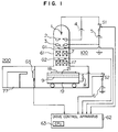
- Fig. 1 is a schematic structural diagram of a scanning electron microscope system according to an embodiment of the invention. This microscope system is arranged by a scanning electron microscope main body 100 and a sample replacing mechanism 200.
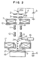
- Fig. 2 schematically represents a structure of the scanning electron microscope main body 100 shown in Fig. 1.
- a cathode 1, a draw-out electrode 2, and an anode 3 constitute a field-emission-type electron gun.
- a draw-out voltage 4 is applied between the cathode 1 and draw- out electrode 2, and an acceleration voltage 5 is applied to the cathode 1.
- An electron beam 20a emitted from the cathode 1 is further accelerated by the voltage applied between the draw-out electrode 2 and anode 3 biased at the ground potential.
- acceleration voltage energy (acceleration voltage) of the electron beam passing through the anode 3 coincides with the acceleration voltage 5. Since a voltage of a negative superimposed voltage source 6 is applied via a sample holder 21 to the sample 18, and a retarding static field is produced between an objective lense 17 and the sample 18, the acceleration voltage of the electron beam illuminated, or irradiated to the sample 18 is equal to a voltage obtained by subtracting the voltage of the negative superimposed voltage source 6 from the acceleration voltage 5.
- the electron beam 20b accelerated as the result of passing through the anode 3 is focused onto the sample 18 by a condenser lens 7 and the objective lense 17.
- the electron beam passing through the objective lense 17 is decelerated by the retarding static field formed between the objective lense 17 and the sample 18, and reaches the sample 18 at energy corresponding to the voltage obtained by essentially subtracting the voltage of the superimposed voltage source 6 from the acceleration voltage.
- the divergence angle of the electron beam at the objective lens 17 is determined by an aperture 8 set under the condenser lens 7. Centering of the aperture 8 is performed by operating an adjusting knob 10.
- the accelerated electron beam 20b is deflected by an upper scanning coil 11 and a lower scanning coil 12.
- the focused electron beam 20c which has been decelerated by the retarding static field is scanned on the sample 18 in a raster-like fashion.
- the scanning coils are arranged in two stages, so that the scanned electron beam always passes through the center of the objective lens 17.
- the sample 18 is fixed by a sample holder 21, and the sample holder 21 is mounted via an insulating table 9 on a sample stage 19 whose position is adjustable along the horizontal direction and the like.
- the voltage of the superimposed voltage source 6 is applied to the sample holder 21.
- Secondary electrons 24 emitted from the sample 18 to which the decelerated electron beam 20c is irradiated, are accelerated by the retarding static field produced between the objective lens 17 and the sample 18, and then are extracted within the objective lens 17, and furthermore are climbed up in a spiral motion while being influenced by the magnetic field of the objective lens 17.
- the secondary electrons 24 passing through the objective lens 17 are absorbed by an extraction electrode 13 which is provided outside the electron beam path and between the objective lens 17 and the lower scanning coil 12, to which a positive potential is applied. Then, the secondary electrons 24 are extracted and accelerated by a scintillator 14 to which a positive potential of 10 KV is applied, so that the scintillator 14 is illuminated.
- the emitted light is directed to a photomultiplier tube 16 by a light guide 15 and converted into electric signals.
- the output of the photomultiplier tube 16 is further amplified to serve as the brightness modulation input of a cathode ray tube.
- the diagram showing the process is not illustrated.
- the primary electron beam irradiated to the sample is retarded or decelerated, thereby having low energy, the charging-up of the sample can be solved.
- the beam diameter was 15 nm when only the acceleration voltage of 500 V was applied.
- the beam diameter could be advantageously 10 nm when the acceleration voltage of 1,000 V was superimposed with the superimposed voltage of 500 V.
- the constructive elements such as the field emitting cathode 1, the draw-out electrode 2, the anode 3, the condenser lens 7, the objective lens 17, the sample 18, the sample holder 21, the insulating stage 9, and the sample stage 19, are contained within a vacuum chamber 61. It should be noted that the vacuum exhausting system is omitted from Fig. 1.
- the above-described control of the switch S2 is executed by way of a drive control apparatus 62.
- This drive control apparatus controls an overall operation of the scanning electron microscope system in accordance with operations of a CPU (central processing unit) 63.
- CPU central processing unit
- the drive control apparatus 62 drives to open and close the switches S1, S2 and the valves G1, G2, G3 respectively in accordance with an instruction issued from the CPU 63, and also confirms whether or not the drive control has been executed in response to the instruction.
- the control operation to turn ON/OFF the switch S2 so as to apply the superimposed voltage is also performed in accordance with a flow chart shown in Fig. 3.
- a check is made as to whether or not the switch S1 for acceleration voltage is closed at a step S64. If the check result become YES, then another check is done as to whether or not the valves G1 and G2 provided on the electron beam path are opened at a step 65.
- the control process is advanced to a step 66 at which a judgement is made as to whether or not the valve G3 provided on the path along which the sample is inserted and extracted, is closed.
- the switch S2 for applying the superimposed voltage is closed the superimposed voltage to the sample. If even one judgement result becomes NO at the above-explained steps 64 to 66, then since any one of the three conditions cannot be satisfied, the switch S2 is opened at a step 68, so that no superimposed voltage is applied to the sample.
- sample holder 21 is electrically connected via a discharge resistor R to the sample stage 19, when the switch S2 is opened, the electrons charged on the sample 18 are quickly discharged through the sample holder 21, the discharge resistor R and the sample stage 19 under a preselected time constant, and thus the potential of the sample 18 become the ground potential.
- valves G1 and G2 are opened either only when the acceleration voltage 5 is applicable under a certain condition that a vacuum degree around the cathode 1 is higher than a preset value, or only when a vacuum degree of the vacuum chamber 61 is higher than a preset value.
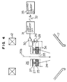
- Fig. 4 is a schematic structural diagram for showing a secondary electron detecting unit of a scanning electron microscope according to a second embodiment of the present invention, in which the same symbols as those of the first embodiment represent the same or equivalent portions.
- the first embodiment shown in Fig. 2 detects the secondary electrons 24 by directing them to the outside of the electron beam path by the absorbing electrode 13. However, in the second embodiment, the secondary electrons are detected by a multi-channel plate detector 26.
- a disk-shaped multi-channel plate main body 25 having a central hole 33 is employed between the objective lens 17 and the lower scanning coil 12.
- a diameter of the central hole 33 is selected to be such a size that the electron beam 20b deflected by the lower scanning coil 12 does not collide with this central hole 33.
- a mesh 34 is provided under the multi-channel plate main body 25.
- the electron beam 20b is focused by the objective lens 17 and then irradiated on the sample 18.
- the secondary electrons 24 emitted from the sample 18 undergo the lens-action of the objective lens 17, pass through the mesh 34 set on the front surface while diverging, and enter the multi-channel plate 25.
- the secondary electrons 24 having entered the multi-channel plate 25 are accelerated and amplified by an amplifying voltage 28 applied to both ends of the multi-channel plate 25.
- the amplified electrons 27 are further accelerated by the anode voltage 29 and captured by the anode 37
- the captured secondary electrons After the captured secondary electrons have been amplified by an amplifier 30, they are converted into light by light converting circuit 31.
- the reason whey the secondary electrons are converted into the light 32, is such that the amplifier 30 is brought in a floating state due to the amplifying voltage 28 of the multi-channel plate 25, and so forth.
- the light 32 is converted into electric signals again by an electricity converting circuit 35 for a ground potential and used as the brightness modulation signal for the scanning image. According to this method, only the secondary electrons but also the backscatterd electrons may be detected.
- Fig. 5 is a schematic structural diagram for showing a secondary electron detecting unit of a scanning electron microscope according to a third embodiment of the present invention, in which the same symbols as those of the second embodiment represent the same or equivalent portions.
- the third embodiment is characterized in that desired secondary signals can be selectively detected.
- a filtering voltage capable of optionally controlling the potential of the channel plate 25 is applied to the channel plate 25 from a power source 36.
- the filtering voltage from the power source 36 is assumed to be a negative voltage of approximately 10 V lower than the superimposed voltage from the power source 6, the secondary electrons among the secondary electrons and the backscatterd electrons emitted from a sample are repelled by an inverse electric field produced between the channel plate 25 and mesh 33, and only the backscatterd electrons having higher energy can be selectively detected.
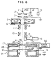
- Fig. 6 is a schematic structural diagram for representing a secondary electron detecting unit of a scanning electron microscope according to a fourth embodiment of the present invention, in which the same reference numerals are employed as those for denoting the same or similar components.
- This embodiment is to provide an energy filter, namely a potential barrier above the objective lens 17.
- an in-lens method that the sample 18 is arranged within the objective lens 17.
- the energy filter is constructed of a cylinder 46, one pair of shield grids 41, and a filtering grid 42. Similarly to the third embodiment in Fig. 4, this embodiment makes it possible to measure the potential of the sample 18 by controlling the filtering voltage to properly adjust the potential of the filtering grid 42.
- this embodiment makes it possible to selectively detect only secondary electrons without detecting backscatterd electrons by properly selecting the voltage of the extraction electrode 13.
- the sample stage 19 is disposed inside the objective lens 17, an the sample 18 is fixed via the insulating stage 9 and the sample holder 21 to the sample stage 19.
- the superimposed voltage 6 is applied to a sample holder 21, and a retarding static field is produced between the sample 18 and the objective lens 17.
- An energizing coil 45 of the objective lens 17 is fixed on the upper portion of the objective lens 17.
- the objective 17 is large enough to house 8-inch wafers.
- Fig. 7 is a schematic structural diagram for showing a secondary electron detecting unit of a scanning electron microscope according to a fifth embodiment of the present invention, in which the same symbols as those of the fourth embodiment represent the same or equivalent portions. This embodiment is capable of observing a sample which may be damaged if a strong electric field would be applied to it.
- an element may be broken down by a strong electric field.
- this embodiment is provided with a control electrode 39 between the objective lens 17 and the sample 18 to apply several tens of voltage derived from a control voltage source 40 to the control electrode 39.
- the electric field produced between the objective lens 17 and the sample 18 is relaxed by way of the control electrode 39, so that it may be prevent a destroy of the element.
- Fig. 8 is a schematic structural diagram for showing a secondary electron detecting unit of a scanning electron microscope according to a sixth embodiment of the present invention, in which the same symbols as those of the fifth embodiment represent the same or equivalent portions.
- the secondary signals are deflected by utilizing the electric field and then the deflected secondary signal is detected by the detector.
- the secondary particles are deflected by utilizing the magnetic field and the electric field.
- an electric field "E" generated by the extraction electrode 13 for extracting the secondary electrons 24 bends not only the secondary electrons 24 but also the primary electron beam 20b.
- the present embodiment solves this problem by taking account of such a fact that the direction of deflection of an electron beam due to a magnetic field "B" depends on progress direction of the electron beam deflection of the primary electron beam 20b due to the electric field "E” is canceled by the magnetic field "B” and the magnetic field supplements the deflection of the secondary electrons 24.
- this embodiment generates the magnetic field B in such a manner that the primary electron beam 22b is deflected in the direction opposite to the direction of deflection caused by the electric field E generated by the extraction electrode 13. Therefore, the deflection of the electron beam 22b due to the electric field E is canceled by properly controlling the magnitude of the magnetic field B.
- Fig. 9 is a schematic structural diagram for showing a secondary electron detecting unit of a scanning electron microscope according to a seventh embodiment of the present invention, in which the same symbols as those of the sixth embodiment indicate the same or equivalent portions.
- secondary signals are detected by utilizing a single crystal scintillator.
- a single crystal scintillator 55 is constructed such that, for example, a cylindrical YAG single crystal is obliquely cut, an opening 57 for passing the primary electrons 20b is formed in the cut surface, the tip portion of the scintillator 55 is coated with a conductive thin film 56 made of metal or carbon, and the ground potential is given to the thin film 56.
- the crossover 58 of the primary electron beam 20b produced by the condenser lens 7 is positioned near the opening 57 and the crossover 59 of the secondary electrons 24 by the objective lens 17 is positioned apart from the opening 57. Accordingly, the secondary electrons 24 can be efficiently detected, while the primary electron beam 20b is not shielded by the opening 57.
- the above seventh embodiment describes such that the light emitting portion of the scintillator and the light guide are arranged by the YAG single crystal.
- the light emitting portion of the scintillator for detecting the secondary electrons may be formed by the YAG single crystal, and other portions thereof may be fabricated by such a transparent member as glass and resin.
- Fig. 10 is a schematic structural diagram for indicating a secondary electron detecting unit of a major portion of a scanning electron microscope according to an eighth embodiment of the present invention, in which the same symbols as those of the seventh embodiment represent the same or equivalent portions.
- an anode for constructing an electron gun is omitted, and an electron beam is accelerated by the draw-out voltage 4 applied between the draw-out electrode 2 connected to the ground potential and the cathode 1.
- the electrons accelerated by the draw-out voltage 4 are converged by the objective lens 17 and then are directed toward the sample 18.
- a positive polarity of the acceleration voltage source 5 is connected to the sample 18. At this time, since the voltage of the acceleration voltage source 5 is higher than the voltage of the draw-out voltage source 4 in the low acceleration voltage region, the electron beam is decelerated by the acceleration voltage 5 between the objective lens 17 and the sample 18 and then reaches the sample.
- the draw-out voltage is 3 KV and the acceleration voltage is 1 KV.
Abstract
Description
- The present invention generally relates to a scanning electron microscope for obtaining a scanning image by scanning an electron spot on a sample, and particularly to a scanning electron microscope capable of obtaining a scanning image with high spatial resolution within a low acceleration voltage region.
- A scanning electron microscope has been conventionally used for observation and a length-measurement of submicron-order (1 micron or less), such as contact holes and line patterns in a semiconductor device sample.
- The scanning electron microscope obtains a scanning image (SEM image) by scanning an electron beam emitted from a heating type or field emission type electron source on a sample to detect secondary particles such as secondary electrons and back scattered electrons as detection signals, and using the detection signals for the brightness modulation input for a cathode ray tube scanned synchronously with the electron beam scanning. In typical scanning electron microscopes, electrons emitted from an electron source are accelerated between the electron source to which a negative potential is being applied and an anode connected to the ground potential. The accelerated electrons are focused on the sample connected to the ground potential.
- Very recently, scanning electron microscopes have been used in manufacturing process and inspections of semiconductor devices. For this purpose, a need has arisen for achieving high resolution below than 10 nm with employment of such a low acceleration voltage less than 1,000V in order to observe an insulating material without any charging-up effect.
- That is, a semiconductor device sample is generally made by forming an electrical insulator such as SiO₂ or SiN on a conductive portion of Al or Si. When an electron beam is applied to the semiconductor device sample, the surface of the electrical insulation is negatively electrified (hereafter may be expressed simply as "changing-up"), orbit of the emitted electrons is changed, and orbit of the primary electrons per se is changed. As a result, abnormal contrast or distortion may occur in the SEM (scanning electron microscope) image.
- The above image interference due to charging-up seriously affects the observation of contact holes and the length-measurement of lines-and-spaces. Therefore, this makes it difficult to not only evaluate semiconductor manufacturing processes, but also assure the quality of semiconductor devices. For this reason, a so-called low voltage acceleration SEM has been conventionally used in which the energy of the primary electron beam which scans on a sample is 1 keV or lower.
- However, the above-described prior art owns the following various problems. That is, if the acceleration voltage would become lower, observation at a high magnification would become difficult because the resolution is extremely degraded due to increase of chromatic aberration caused by energy spread of electron beams. If electron current would decrease, the ratio of secondary signal to noise (S/N) would extremely decrease, the contrast of an SEM image is impaired, and observation at high magnification and resolution would become difficult. Especially, for a semiconductor device made by an ultra-fine processing technique, signals generated from recessed portions of contact holes and line patterns become weak. Therefore, this makes fine observation and length-measurement very difficult.
- To solve such a problem, some methods have been proposed. For instance, in accordance with proceeding of IEEE 9th Annual Symposium on Electron, Ion and Laser Technology, pages 176 to 186, the acceleration voltage applied between the electron source and the anode biased at the ground potential is set to the high value, and the retarding static field is produced between the objective lense biased at the ground potential and the inspection sample to which the negative potential is applied, so that the electron beams irradiated to the sample are decelerated. Thus, the acceleration voltage is eventually set to a relatively low voltage, and such a scanning electron microscope is proposed that both chromatic aberration can be reduced and the changing-up can be prevented.
- Nevertheless, since the applications of negative potentials to the sample are manually performed by operators in this prior art scanning electron microscope, there are some possibilities that a shortcircuit happens to occurs between the sample and the ground potential when operators would forget to cut off the application of negative potentials to the sample during substitution of the sample. Moreover, there are possibilities that samples such as semiconductor devices which are readily, adversely influenced by electric damages may be destroyed due to sudden potential changes caused by the shortcircuit. As a consequence, there are various problems. That is, a careful operation is required when the voltage application is turned ON/OFF while the sample is mounted and replaced in the scanning electron microscope, i.e., a difficult handling of the sample is needed.
- An object of the present invention has been made to solve the above-described conventional problems, and therefor to provide a scanning electron microscope capable of easily mounting and relating a sample with respect to such a scanning electron microscope that a retarding static field for electron beams is produced between an objective lens and the sample.
- To achieve the above-explained object, according to the present invention, in a scanning electron microscope wherein primary electron beams emitted from an electron source are scanned on a sample, and a scanning image is obtained from a detection signal produced by secondary particles generated from the sample, there are provided:
means for detecting the secondary particles generated from a surface of the sample on the side of the electron source separated from an objective lens;
means for producing a retarding static field with respect to the primary electron beams between the sample and the objective lens by applying a negative voltage to the sample; and
means for controlling an application of the negative voltage to the sample in conjunction with a preparation operation for mounting and replacing the sample. - With the above-described arrangement, since the application of negative voltage to the sample is controlled in conjunction with the preparation operation for mounting and replacing the sample, operators can mount and replace the sample without paying their specific attentions to the application of negative voltage to the sample, resulting in very easy handling.
- For a more complete understanding of the present invention, and the advantages thereof, reference is now made of the following descriptions taken in conjunction with the accompanying drawings, in which:
- Fig. 1 is a schematic structural diagram of a scanning electron microscope according to a first embodiment of the present invention;
- Fig. 2 is a schematic structural diagram of the scanning electron microscope unit shown in Fig. 1;
- Fig. 3 is a flow chart for representing a major operation of the scanning electron microscope according to the present invention;
- Fig. 4 is a schematic structural diagram of another scanning electron microscope unit according to a second embodiment of the present invention;
- Fig. 5 is a schematic structural diagram of another scanning electron microscope unit according to a third embodiment of the present invention;
- Fig. 6 is a schematic structural diagram of another scanning electron microscope unit according to a fourth embodiment of the present invention;
- Fig. 7 is a schematic structural diagram of another scanning electron microscope unit according to a fifth embodiment of the present invention;
- Fig. 8 is a schematic structural diagram of another scanning electron microscope unit according to a sixth embodiment of the present invention;
- Fig. 9 is a schematic structural diagram of a further scanning electron microscope unit according to a seventh embodiment of the present invention; and
- Fig. 10 is a schematic structural diagram of a still further scanning electron microscope unit according to an eighth embodiment of the present invention.
- Referring now to drawings, the present invention will be described in detail.
- Fig. 1 is a schematic structural diagram of a scanning electron microscope system according to an embodiment of the invention. This microscope system is arranged by a scanning electron microscope
main body 100 and asample replacing mechanism 200. Fig. 2 schematically represents a structure of the scanning electron microscopemain body 100 shown in Fig. 1. - In Fig. 2, a cathode 1, a draw-out
electrode 2, and ananode 3 constitute a field-emission-type electron gun. A draw-outvoltage 4 is applied between the cathode 1 and draw- outelectrode 2, and an acceleration voltage 5 is applied to the cathode 1. Anelectron beam 20a emitted from the cathode 1 is further accelerated by the voltage applied between the draw-outelectrode 2 andanode 3 biased at the ground potential. - As a result, energy (acceleration voltage) of the electron beam passing through the
anode 3 coincides with the acceleration voltage 5. Since a voltage of a negative superimposedvoltage source 6 is applied via asample holder 21 to thesample 18, and a retarding static field is produced between anobjective lense 17 and thesample 18, the acceleration voltage of the electron beam illuminated, or irradiated to thesample 18 is equal to a voltage obtained by subtracting the voltage of the negativesuperimposed voltage source 6 from the acceleration voltage 5. - The
electron beam 20b accelerated as the result of passing through theanode 3 is focused onto thesample 18 by acondenser lens 7 and theobjective lense 17. The electron beam passing through theobjective lense 17 is decelerated by the retarding static field formed between theobjective lense 17 and thesample 18, and reaches thesample 18 at energy corresponding to the voltage obtained by essentially subtracting the voltage of thesuperimposed voltage source 6 from the acceleration voltage. - The divergence angle of the electron beam at the
objective lens 17 is determined by anaperture 8 set under thecondenser lens 7. Centering of theaperture 8 is performed by operating an adjustingknob 10. - The accelerated
electron beam 20b is deflected by an upper scanning coil 11 and alower scanning coil 12. The focusedelectron beam 20c which has been decelerated by the retarding static field is scanned on thesample 18 in a raster-like fashion. In this embodiment, the scanning coils are arranged in two stages, so that the scanned electron beam always passes through the center of theobjective lens 17. - The
sample 18 is fixed by asample holder 21, and thesample holder 21 is mounted via an insulating table 9 on asample stage 19 whose position is adjustable along the horizontal direction and the like. The voltage of thesuperimposed voltage source 6 is applied to thesample holder 21. -
Secondary electrons 24 emitted from thesample 18 to which the deceleratedelectron beam 20c is irradiated, are accelerated by the retarding static field produced between theobjective lens 17 and thesample 18, and then are extracted within theobjective lens 17, and furthermore are climbed up in a spiral motion while being influenced by the magnetic field of theobjective lens 17. - The
secondary electrons 24 passing through theobjective lens 17 are absorbed by anextraction electrode 13 which is provided outside the electron beam path and between theobjective lens 17 and thelower scanning coil 12, to which a positive potential is applied. Then, thesecondary electrons 24 are extracted and accelerated by ascintillator 14 to which a positive potential of 10 KV is applied, so that thescintillator 14 is illuminated. - The emitted light is directed to a
photomultiplier tube 16 by alight guide 15 and converted into electric signals. The output of thephotomultiplier tube 16 is further amplified to serve as the brightness modulation input of a cathode ray tube. However, the diagram showing the process is not illustrated. - In accordance with the scanning electron microscope with such a structural arrangement, as described above, since energy of the
electron beam 20b when passing through thecondenser lens 7, theaperture 8, and theobjective lens 17 is higher than that of theelectron beam 20c at the final stage, chromatic aberration could be improved and higher resolution could be achieved, as compared with those of the conventional microscope system. - Moreover, since the primary electron beam irradiated to the sample is retarded or decelerated, thereby having low energy, the charging-up of the sample can be solved.
- Concretely speaking, the beam diameter was 15 nm when only the acceleration voltage of 500 V was applied. To the contrary, the beam diameter could be advantageously 10 nm when the acceleration voltage of 1,000 V was superimposed with the superimposed voltage of 500 V.
- In Fig. 1, the constructive elements such as the field emitting cathode 1, the draw-out
electrode 2, theanode 3, thecondenser lens 7, theobjective lens 17, thesample 18, thesample holder 21, the insulatingstage 9, and thesample stage 19, are contained within avacuum chamber 61. It should be noted that the vacuum exhausting system is omitted from Fig. 1. - It should also be noted that under such a condition that the negative voltage is being applied to the
sample 18, it must be avoided that the sample replacement by asample replacing mechanism 77 and thevacuum chamber 61 are under atmospheric pressure. In other words, the voltage of the superimposedpower source 6 may be applied only when the electron beam is scanned on thesample 18. - Therefore, according to the present invention, only when all of the following first to third conditions which are preparation operations for mounting/replacing the sample, are satisfied, such a control to close a switch S2 is performed in such a manner that the voltage of the superimposed
voltage source 6 is applied to thesample 18. In the first condition, a switch S1 is closed to apply the acceleration voltage 5. In the second condition, both of a valve G1 and a valve G2, which are provided between the cathode 1 and thesample 18, are opened. In the third condition, a valve G3 for causing the sample to pass therethrough is closed when thesample 18 is mounted on thesample stage 19 by using thesample replacing mechanism 77. - The above-described control of the switch S2 is executed by way of a
drive control apparatus 62. This drive control apparatus controls an overall operation of the scanning electron microscope system in accordance with operations of a CPU (central processing unit) 63. In particular, only a control operation of the switch S2 will now be explained. - The
drive control apparatus 62 drives to open and close the switches S1, S2 and the valves G1, G2, G3 respectively in accordance with an instruction issued from theCPU 63, and also confirms whether or not the drive control has been executed in response to the instruction. Here, the control operation to turn ON/OFF the switch S2 so as to apply the superimposed voltage is also performed in accordance with a flow chart shown in Fig. 3. First, a check is made as to whether or not the switch S1 for acceleration voltage is closed at a step S64. If the check result become YES, then another check is done as to whether or not the valves G1 and G2 provided on the electron beam path are opened at astep 65. At this step, if the check result becomes YES, then the control process is advanced to astep 66 at which a judgement is made as to whether or not the valve G3 provided on the path along which the sample is inserted and extracted, is closed. At this step, if the judgement result becomes YES, then since all of the above-described first, second and third conditions can be satisfied, the switch S2 for applying the superimposed voltage is closed the superimposed voltage to the sample. If even one judgement result becomes NO at the above-explainedsteps 64 to 66, then since any one of the three conditions cannot be satisfied, the switch S2 is opened at astep 68, so that no superimposed voltage is applied to the sample. - It should be noted that the
sample holder 21 is electrically connected via a discharge resistor R to thesample stage 19, when the switch S2 is opened, the electrons charged on thesample 18 are quickly discharged through thesample holder 21, the discharge resistor R and thesample stage 19 under a preselected time constant, and thus the potential of thesample 18 become the ground potential. - It should also be noted that such a normal sequence that the valves G1 and G2 are opened either only when the acceleration voltage 5 is applicable under a certain condition that a vacuum degree around the cathode 1 is higher than a preset value, or only when a vacuum degree of the
vacuum chamber 61 is higher than a preset value. - Although there has been described in this embodiment that when all of the above-explained three conditions could be satisfied, the superimposed
voltage 6 was applied, when either one or two conditions among them can be satisfied, the switch S2 may be closed. - Fig. 4 is a schematic structural diagram for showing a secondary electron detecting unit of a scanning electron microscope according to a second embodiment of the present invention, in which the same symbols as those of the first embodiment represent the same or equivalent portions.
- The first embodiment shown in Fig. 2 detects the
secondary electrons 24 by directing them to the outside of the electron beam path by the absorbingelectrode 13. However, in the second embodiment, the secondary electrons are detected by amulti-channel plate detector 26. - In this drawing, a disk-shaped multi-channel plate
main body 25 having acentral hole 33 is employed between theobjective lens 17 and thelower scanning coil 12. A diameter of thecentral hole 33 is selected to be such a size that theelectron beam 20b deflected by thelower scanning coil 12 does not collide with thiscentral hole 33. Amesh 34 is provided under the multi-channel platemain body 25. - With such a structure, after the accelerated
electron beam 20b has passed through thecentral hole 33 of the multi- channel platemain body 25, theelectron beam 20b is focused by theobjective lens 17 and then irradiated on thesample 18. Thesecondary electrons 24 emitted from thesample 18 undergo the lens-action of theobjective lens 17, pass through themesh 34 set on the front surface while diverging, and enter themulti-channel plate 25. Thesecondary electrons 24 having entered themulti-channel plate 25 are accelerated and amplified by an amplifyingvoltage 28 applied to both ends of themulti-channel plate 25. The amplifiedelectrons 27 are further accelerated by theanode voltage 29 and captured by theanode 37 - After the captured secondary electrons have been amplified by an
amplifier 30, they are converted into light by light convertingcircuit 31. The reason whey the secondary electrons are converted into the light 32, is such that theamplifier 30 is brought in a floating state due to the amplifyingvoltage 28 of themulti-channel plate 25, and so forth. - The light 32 is converted into electric signals again by an
electricity converting circuit 35 for a ground potential and used as the brightness modulation signal for the scanning image. According to this method, only the secondary electrons but also the backscatterd electrons may be detected. - As apparent from the foregoing description, similar advantages to the previous embodiment can be achieved by this embodiment.
- Fig. 5 is a schematic structural diagram for showing a secondary electron detecting unit of a scanning electron microscope according to a third embodiment of the present invention, in which the same symbols as those of the second embodiment represent the same or equivalent portions. The third embodiment is characterized in that desired secondary signals can be selectively detected.
- In this drawing, a filtering voltage capable of optionally controlling the potential of the
channel plate 25 is applied to thechannel plate 25 from apower source 36. For example, when the filtering voltage from thepower source 36 is assumed to be a negative voltage of approximately 10 V lower than the superimposed voltage from thepower source 6, the secondary electrons among the secondary electrons and the backscatterd electrons emitted from a sample are repelled by an inverse electric field produced between thechannel plate 25 andmesh 33, and only the backscatterd electrons having higher energy can be selectively detected. - It is also possible to find the potential of the sample by measuring the filtering voltage which is a limit for repelling secondary electrons. Thus, it is possible to inspect the functions of finished semiconductor devices by adding such a function.
- Fig. 6 is a schematic structural diagram for representing a secondary electron detecting unit of a scanning electron microscope according to a fourth embodiment of the present invention, in which the same reference numerals are employed as those for denoting the same or similar components. This embodiment is to provide an energy filter, namely a potential barrier above the
objective lens 17. Especially, in accordance with the present embodiment, there is represented an in-lens method that thesample 18 is arranged within theobjective lens 17. - The energy filter is constructed of a
cylinder 46, one pair ofshield grids 41, and afiltering grid 42. Similarly to the third embodiment in Fig. 4, this embodiment makes it possible to measure the potential of thesample 18 by controlling the filtering voltage to properly adjust the potential of thefiltering grid 42. - Moreover, this embodiment makes it possible to selectively detect only secondary electrons without detecting backscatterd electrons by properly selecting the voltage of the
extraction electrode 13. - In this in-lens system, the
sample stage 19 is disposed inside theobjective lens 17, an thesample 18 is fixed via the insulatingstage 9 and thesample holder 21 to thesample stage 19. The superimposedvoltage 6 is applied to asample holder 21, and a retarding static field is produced between thesample 18 and theobjective lens 17. An energizingcoil 45 of theobjective lens 17 is fixed on the upper portion of theobjective lens 17. The objective 17 is large enough to house 8-inch wafers. - Fig. 7 is a schematic structural diagram for showing a secondary electron detecting unit of a scanning electron microscope according to a fifth embodiment of the present invention, in which the same symbols as those of the fourth embodiment represent the same or equivalent portions. This embodiment is capable of observing a sample which may be damaged if a strong electric field would be applied to it.
- In semiconductor integrated circuits, an element may be broken down by a strong electric field. To solve the problem, this embodiment is provided with a
control electrode 39 between theobjective lens 17 and thesample 18 to apply several tens of voltage derived from acontrol voltage source 40 to thecontrol electrode 39. - In accordance with this embodiment, the electric field produced between the
objective lens 17 and thesample 18 is relaxed by way of thecontrol electrode 39, so that it may be prevent a destroy of the element. - Fig. 8 is a schematic structural diagram for showing a secondary electron detecting unit of a scanning electron microscope according to a sixth embodiment of the present invention, in which the same symbols as those of the fifth embodiment represent the same or equivalent portions.
- In the above-described first and fourth embodiments, the secondary signals are deflected by utilizing the electric field and then the deflected secondary signal is detected by the detector. In this embodiment, the secondary particles are deflected by utilizing the magnetic field and the electric field.
- When the retarding voltage increases and then the energy difference between the
primary electron beam 20b and thesecondary electrons 24 emitted from the sample and accelerated by the retarding static field decreases. Therefore, an electric field "E" generated by theextraction electrode 13 for extracting thesecondary electrons 24 bends not only thesecondary electrons 24 but also theprimary electron beam 20b. - The present embodiment solves this problem by taking account of such a fact that the direction of deflection of an electron beam due to a magnetic field "B" depends on progress direction of the electron beam deflection of the
primary electron beam 20b due to the electric field "E" is canceled by the magnetic field "B" and the magnetic field supplements the deflection of thesecondary electrons 24. - That is, this embodiment generates the magnetic field B in such a manner that the primary electron beam 22b is deflected in the direction opposite to the direction of deflection caused by the electric field E generated by the
extraction electrode 13. Therefore, the deflection of the electron beam 22b due to the electric field E is canceled by properly controlling the magnitude of the magnetic field B. - On the other hand, because the direction of deflection of secondary electrons due to the magnetic field B is the same as that due to the electric field E, the deflection amount of the secondary electrons increases and the secondary electrons can be easily detected.
- Fig. 9 is a schematic structural diagram for showing a secondary electron detecting unit of a scanning electron microscope according to a seventh embodiment of the present invention, in which the same symbols as those of the sixth embodiment indicate the same or equivalent portions. In this embodiment, secondary signals are detected by utilizing a single crystal scintillator.
- In this drawing, a
single crystal scintillator 55 is constructed such that, for example, a cylindrical YAG single crystal is obliquely cut, anopening 57 for passing theprimary electrons 20b is formed in the cut surface, the tip portion of thescintillator 55 is coated with a conductivethin film 56 made of metal or carbon, and the ground potential is given to thethin film 56. - In this embodiment, the
crossover 58 of theprimary electron beam 20b produced by thecondenser lens 7 is positioned near theopening 57 and thecrossover 59 of thesecondary electrons 24 by theobjective lens 17 is positioned apart from theopening 57. Accordingly, thesecondary electrons 24 can be efficiently detected, while theprimary electron beam 20b is not shielded by theopening 57. - It should be understood that the above seventh embodiment describes such that the light emitting portion of the scintillator and the light guide are arranged by the YAG single crystal. Alternatively, only the light emitting portion of the scintillator for detecting the secondary electrons may be formed by the YAG single crystal, and other portions thereof may be fabricated by such a transparent member as glass and resin.
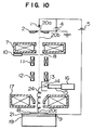
- Fig. 10 is a schematic structural diagram for indicating a secondary electron detecting unit of a major portion of a scanning electron microscope according to an eighth embodiment of the present invention, in which the same symbols as those of the seventh embodiment represent the same or equivalent portions.
- In this embodiment, an anode for constructing an electron gun is omitted, and an electron beam is accelerated by the draw-out
voltage 4 applied between the draw-outelectrode 2 connected to the ground potential and the cathode 1. The electrons accelerated by the draw-outvoltage 4 are converged by theobjective lens 17 and then are directed toward thesample 18. A positive polarity of the acceleration voltage source 5 is connected to thesample 18. At this time, since the voltage of the acceleration voltage source 5 is higher than the voltage of the draw-outvoltage source 4 in the low acceleration voltage region, the electron beam is decelerated by the acceleration voltage 5 between theobjective lens 17 and thesample 18 and then reaches the sample. In the typical example with employment of the field emission cathode, the draw-out voltage is 3 KV and the acceleration voltage is 1 KV. With such a structure, since both of the anode and the superimposed voltage source are omitted, the overall arrangement can be made simple. - As previously described in detail, in accordance with the present invention, in such a scanning electron microscope that the electron beams to be irradiated to the sample are decelerated by producing the retarding static field between the sample and the objective lens while applying the negative potential to the sample, whereby chromatic aberration is reduced and the charging-up is prevented, since the application of the negative potential is automatically controlled in conjunction with the preparation operation for mounting and replacing the sample, operators can mount and replace the sample without paying their specific attentions to the application of negative potential to the sample. As a consequence, the scanning electron microscope system can be very easily handled.
Claims (11)
- A scanning electron microscope wherein primary electron beams emitted from an electron source (1) are scanned on a sample, and a scanning image is obtained from a detection signal produced by secondary particles generated from the sample, comprising:
secondary particle detecting means (13-16, 25) for detecting the secondary particles generated from a surface of the sample (18) on the side of the electron source (1) separated from an objective lens (17);
means (6, 52) for producing a retarding static field with respect to the primary electron beams between the sample (18) and the objective lens (17) by applying a negative voltage to the sample (18); and
means (62, 63) for controlling an application of the negative voltage to the sample (18) in conjunction with a preparation operation for mounting and replacing the sample. - A scanning electron microscope as claimed in claim 1, wherein said preparation operation corresponds to at least one of opening/closing operations for a sample transporting gate valve (G3), opening/closing operations for gate valves (G1, G2) employed in a vacuum chamber, and a control operation to apply an acceleration voltage.
- A scanning electron microscope as claimed in claim 1 or 2, wherein said means for applying the negative voltage to the sample is constructed of:
a sample holder (21) for fixing the sample (18);
a sample stage (19) for mounting the sample holder (21) via an insulating stage (9); and
means (6, 52) for applying the negative voltage to the sample holder (21). - A scanning electron microscope as claimed in claim 3, wherein said sample stage (19) is grounded, and said sample holder (21) is electrically connected via a discharge resistor (R) to the sample stage (19).
- A scanning electron microscope as claimed in claim 1, wherein said secondary particles detecting means (13-16, 25) includes a scintillator (14) provided outside an electron beam path, and an extraction electrode (13) to which a potential to extract the secondary particles is applied, is provided between said scintillator (14) and said electron beam path.
- A scanning electron microscope as claimed in claim 1, wherein said secondary particles detecting means (13-16, 25) is a multi-channel plate detector (25) having an opening (33) at a central portion thereof, which constitutes the electron beam path.
- A scanning electron microscope as claimed in claim 1, wherein said secondary particles detecting means (13-16, 25) is a single crystal scintillator (55).
- A scanning electron microscope as claimed in claim 5, further comprising:
potential barrier generating means (36, 41, 42) provided between said sample (18) and said secondary particles detecting means (13-16, 25) for generating a potential barrier used to select the secondary particles. - A scanning electron microscope as claimed in claim 6, further comprising:
potential barrier generating means (36, 41, 42) provided between said sample (18) and said secondary particles detecting means (13-16, 25) for generating a potential barrier used to select the secondary particles. - A scanning electron microscope as claimed in claim 1, further comprising:
a control electrode (39) provided between said sample (18) and said objective lens (17), for producing an electric field used to relax an influence of the electric field given to the sample (18). - A scanning electron microscope as claimed in claim 5, further comprising:
means for producing a magnetic field perpendicular to said extraction field, which acts to cancel deflection caused by said extraction field with respect to the primary electron beams, and acts to supplement the deflection caused by said extraction field with respect to the secondary particles emitted from the sample (18).
Priority Applications (2)
| Application Number | Priority Date | Filing Date | Title |
|---|---|---|---|
| EP00109452A EP1028452B1 (en) | 1992-10-20 | 1993-10-15 | Scanning electron microscope |
| EP00125870A EP1139385A3 (en) | 1992-10-20 | 1993-10-15 | Scanning electron microscope |
Applications Claiming Priority (3)
| Application Number | Priority Date | Filing Date | Title |
|---|---|---|---|
| JP30620592 | 1992-10-20 | ||
| JP306205/92 | 1992-10-20 | ||
| JP4306205A JP2927627B2 (en) | 1992-10-20 | 1992-10-20 | Scanning electron microscope |
Related Child Applications (4)
| Application Number | Title | Priority Date | Filing Date |
|---|---|---|---|
| EP00125870A Division EP1139385A3 (en) | 1992-10-20 | 1993-10-15 | Scanning electron microscope |
| EP00109452A Division EP1028452B1 (en) | 1992-10-20 | 1993-10-15 | Scanning electron microscope |
| EP00109452.3 Division-Into | 2000-05-03 | ||
| EP00125870.6 Division-Into | 2000-11-24 |
Publications (2)
| Publication Number | Publication Date |
|---|---|
| EP0594084A1 true EP0594084A1 (en) | 1994-04-27 |
| EP0594084B1 EP0594084B1 (en) | 2003-05-21 |
Family
ID=17954262
Family Applications (3)
| Application Number | Title | Priority Date | Filing Date |
|---|---|---|---|
| EP00109452A Expired - Lifetime EP1028452B1 (en) | 1992-10-20 | 1993-10-15 | Scanning electron microscope |
| EP93116733A Expired - Lifetime EP0594084B1 (en) | 1992-10-20 | 1993-10-15 | Scanning electron microscope |
| EP00125870A Withdrawn EP1139385A3 (en) | 1992-10-20 | 1993-10-15 | Scanning electron microscope |
Family Applications Before (1)
| Application Number | Title | Priority Date | Filing Date |
|---|---|---|---|
| EP00109452A Expired - Lifetime EP1028452B1 (en) | 1992-10-20 | 1993-10-15 | Scanning electron microscope |
Family Applications After (1)
| Application Number | Title | Priority Date | Filing Date |
|---|---|---|---|
| EP00125870A Withdrawn EP1139385A3 (en) | 1992-10-20 | 1993-10-15 | Scanning electron microscope |
Country Status (4)
| Country | Link |
|---|---|
| US (1) | US5389787A (en) |
| EP (3) | EP1028452B1 (en) |
| JP (1) | JP2927627B2 (en) |
| DE (1) | DE69332995T2 (en) |
Cited By (8)
| Publication number | Priority date | Publication date | Assignee | Title |
|---|---|---|---|---|
| EP0769799A2 (en) * | 1995-10-19 | 1997-04-23 | Hitachi, Ltd. | Scanning electron microscope |
| WO1998022971A2 (en) * | 1996-11-15 | 1998-05-28 | Leo Electron Microscopy Limited | Scanning electron microscope |
| EP0872873A2 (en) * | 1997-04-18 | 1998-10-21 | Hitachi, Ltd. | Scanning electron microscope |
| US6198299B1 (en) | 1998-08-27 | 2001-03-06 | The Micromanipulator Company, Inc. | High Resolution analytical probe station |
| EP1162645A2 (en) * | 2000-06-09 | 2001-12-12 | Jeol Ltd. | Specimen inspection instrument |
| EP1363395A1 (en) * | 2001-01-25 | 2003-11-19 | Kabushiki Kaisha Toshiba | Method for manufacturing surface acoustic wave device and inspecting instrument |
| US6744268B2 (en) | 1998-08-27 | 2004-06-01 | The Micromanipulator Company, Inc. | High resolution analytical probe station |
| WO2006135939A2 (en) * | 2005-06-16 | 2006-12-21 | Touchstone Research Laboratory, Ltd. | Microsystem manipulation apparatus |
Families Citing this family (39)
| Publication number | Priority date | Publication date | Assignee | Title |
|---|---|---|---|---|
| US5614833A (en) * | 1994-10-25 | 1997-03-25 | International Business Machines Corporation | Objective lens with large field deflection system and homogeneous large area secondary electron extraction field |
| JP3966350B2 (en) * | 1995-10-19 | 2007-08-29 | 株式会社日立製作所 | Scanning electron microscope |
| JP4179369B2 (en) * | 1995-10-19 | 2008-11-12 | 株式会社日立製作所 | Scanning electron microscope |
| JP3774953B2 (en) * | 1995-10-19 | 2006-05-17 | 株式会社日立製作所 | Scanning electron microscope |
| KR100711198B1 (en) * | 1995-10-19 | 2007-07-06 | 가부시끼가이샤 히다치 세이사꾸쇼 | Scanning electron microscope |
| JP4179390B2 (en) * | 1995-10-19 | 2008-11-12 | 株式会社日立製作所 | Scanning electron microscope |
| US6163590A (en) * | 1997-04-08 | 2000-12-19 | X-Ray Technologies Pty Ltd. | High resolution x-ray imaging of very small objects |
| DE19732093B4 (en) | 1997-07-25 | 2008-09-25 | Carl Zeiss Nts Gmbh | Charged particle beam |
| JP3564958B2 (en) * | 1997-08-07 | 2004-09-15 | 株式会社日立製作所 | Inspection method and inspection apparatus using electron beam |
| JP3534582B2 (en) * | 1997-10-02 | 2004-06-07 | 株式会社日立製作所 | Pattern defect inspection method and inspection device |
| WO1999046798A1 (en) * | 1998-03-09 | 1999-09-16 | Hitachi, Ltd. | Scanning electron microscope |
| JP4702295B2 (en) * | 1998-04-20 | 2011-06-15 | 株式会社日立製作所 | Semiconductor manufacturing apparatus and semiconductor inspection apparatus |
| US6509564B1 (en) | 1998-04-20 | 2003-01-21 | Hitachi, Ltd. | Workpiece holder, semiconductor fabricating apparatus, semiconductor inspecting apparatus, circuit pattern inspecting apparatus, charged particle beam application apparatus, calibrating substrate, workpiece holding method, circuit pattern inspecting method, and charged particle beam application method |
| US6426501B1 (en) | 1998-05-27 | 2002-07-30 | Jeol Ltd. | Defect-review SEM, reference sample for adjustment thereof, method for adjustment thereof, and method of inspecting contact holes |
| US6661008B2 (en) | 1998-06-22 | 2003-12-09 | Nikon Corporation | Electron-optical system and inspection method using the same |
| JP4236742B2 (en) | 1998-10-29 | 2009-03-11 | 株式会社日立製作所 | Scanning electron microscope |
| JP4093662B2 (en) * | 1999-01-04 | 2008-06-04 | 株式会社日立製作所 | Scanning electron microscope |
| EP1105914B1 (en) * | 1999-06-22 | 2007-03-07 | Fei Company | Particle-optical apparatus including a particle source that can be switched between high brightness and large beam current |
| US6847038B2 (en) * | 2002-07-15 | 2005-01-25 | Hitachi, Ltd. | Scanning electron microscope |
| WO2001075929A1 (en) * | 2000-03-31 | 2001-10-11 | Hitachi, Ltd. | Scanning electron microscope |
| EP1339100A1 (en) * | 2000-12-01 | 2003-08-27 | Ebara Corporation | Inspection method and apparatus using electron beam, and device production method using it |
| WO2002103337A2 (en) * | 2001-06-15 | 2002-12-27 | Ebara Corporation | Electron beam apparatus and method for using said apparatus |
| DE60118070T2 (en) * | 2001-09-04 | 2006-08-17 | Advantest Corp. | Particle beam apparatus |
| US20040069945A1 (en) * | 2002-10-09 | 2004-04-15 | Taiwan Semiconductor Manufacturing Co., Ltd. | Method for measuring an electrical charge of a photoresist layer |
| US6753533B2 (en) * | 2002-11-04 | 2004-06-22 | Jeol Ltd. | Electron beam apparatus and method of controlling same |
| PL207238B1 (en) * | 2003-10-14 | 2010-11-30 | Politechnika Wroclawska | System for detection of secondary and backward scattered electrons for use in scanning electron microscope |
| US7335879B2 (en) * | 2004-08-16 | 2008-02-26 | Hermes-Microvision, Inc. | System and method for sample charge control |
| JP4634852B2 (en) | 2005-04-25 | 2011-02-16 | 株式会社日立ハイテクノロジーズ | SEM type visual inspection apparatus and inspection method |
| JP4845468B2 (en) * | 2005-10-06 | 2011-12-28 | オリンパス株式会社 | Observation device |
| JP2007324099A (en) * | 2006-06-05 | 2007-12-13 | Hitachi High-Technologies Corp | Sample micromotion system, and charged particle beam device |
| JP4528317B2 (en) | 2007-07-25 | 2010-08-18 | 株式会社日立ハイテクノロジーズ | Visual inspection apparatus equipped with scanning electron microscope and image generation method using scanning electron microscope |
| JP4764436B2 (en) * | 2008-02-14 | 2011-09-07 | 株式会社日立ハイテクノロジーズ | Appearance inspection method and inspection apparatus |
| JP4728361B2 (en) * | 2008-03-06 | 2011-07-20 | 株式会社日立製作所 | Substrate inspection apparatus and substrate inspection method using charged particle beam |
| JP5227643B2 (en) | 2008-04-14 | 2013-07-03 | 株式会社日立ハイテクノロジーズ | An electron beam application device that enables observation with high resolution and high contrast |
| US20090309022A1 (en) * | 2008-06-12 | 2009-12-17 | Hitachi High-Technologies Corporation | Apparatus for inspecting a substrate, a method of inspecting a substrate, a scanning electron microscope, and a method of producing an image using a scanning electron microscope |
| JP5276921B2 (en) | 2008-08-08 | 2013-08-28 | 株式会社日立ハイテクノロジーズ | Inspection device |
| US9202667B2 (en) | 2009-02-19 | 2015-12-01 | Hitachi High-Technologies Corporation | Charged particle radiation device with bandpass detection |
| DE102010008296A1 (en) * | 2010-02-17 | 2011-08-18 | Carl Zeiss NTS GmbH, 73447 | Laser processing system, object holder and laser processing method |
| US8759764B2 (en) * | 2012-06-29 | 2014-06-24 | Fei Company | On-axis detector for charged particle beam system |
Citations (5)
| Publication number | Priority date | Publication date | Assignee | Title |
|---|---|---|---|---|
| JPS5648044A (en) * | 1979-09-28 | 1981-05-01 | Hitachi Ltd | Electron beam device |
| JPS60212954A (en) * | 1984-04-09 | 1985-10-25 | Hitachi Ltd | Electron microscope |
| JPH01115042A (en) * | 1987-10-28 | 1989-05-08 | Hitachi Ltd | Sample stand of scanning type electronic microscope |
| JPH02142045A (en) * | 1988-11-24 | 1990-05-31 | Hitachi Ltd | Scan type electron microscope and similar device thereof |
| JPH0371544A (en) * | 1989-08-11 | 1991-03-27 | Hitachi Ltd | Charged particle beam device |
Family Cites Families (11)
| Publication number | Priority date | Publication date | Assignee | Title |
|---|---|---|---|---|
| JPS478874Y1 (en) * | 1967-10-25 | 1972-04-04 | ||
| NL7100609A (en) * | 1970-02-07 | 1971-08-10 | ||
| DE2005682C3 (en) * | 1970-02-07 | 1974-05-09 | Siemens Ag, 1000 Berlin Und 8000 Muenchen | Device for extracting the secondary electrons in a scanning electron microscope or an electron beam microanalyser |
| US3792263A (en) * | 1972-09-13 | 1974-02-12 | Jeol Ltd | Scanning electron microscope with means to remove low energy electrons from the primary electron beam |
| JPS5132435A (en) * | 1974-09-13 | 1976-03-19 | Furukawa Electric Co Ltd | GINNOHEIKATSU DENCHAKUHO |
| JPS52123163A (en) * | 1976-04-09 | 1977-10-17 | Hitachi Ltd | Reflection electron image observation unit for scanning type electroni c microscope |
| JPS55104059A (en) * | 1979-02-05 | 1980-08-09 | Hitachi Ltd | Electric field radiation type electron microscope |
| US4926054A (en) * | 1988-03-17 | 1990-05-15 | Ict Integrated Circuit Testing Gesellschaft Fur Halbleiterpruftechnik Mbh | Objective lens for focusing charged particles in an electron microscope |
| JPH0349142A (en) * | 1989-07-17 | 1991-03-01 | Hitachi Ltd | Scanning type electron microscope and similar device thereof |
| JPH03295142A (en) * | 1990-04-13 | 1991-12-26 | Hitachi Ltd | Scanning electron microscope |
| JP2919170B2 (en) * | 1992-03-19 | 1999-07-12 | 株式会社日立製作所 | Scanning electron microscope |
-
1992
- 1992-10-20 JP JP4306205A patent/JP2927627B2/en not_active Expired - Lifetime
-
1993
- 1993-10-15 EP EP00109452A patent/EP1028452B1/en not_active Expired - Lifetime
- 1993-10-15 EP EP93116733A patent/EP0594084B1/en not_active Expired - Lifetime
- 1993-10-15 DE DE69332995T patent/DE69332995T2/en not_active Expired - Fee Related
- 1993-10-15 EP EP00125870A patent/EP1139385A3/en not_active Withdrawn
- 1993-10-19 US US08/137,976 patent/US5389787A/en not_active Expired - Lifetime
Patent Citations (5)
| Publication number | Priority date | Publication date | Assignee | Title |
|---|---|---|---|---|
| JPS5648044A (en) * | 1979-09-28 | 1981-05-01 | Hitachi Ltd | Electron beam device |
| JPS60212954A (en) * | 1984-04-09 | 1985-10-25 | Hitachi Ltd | Electron microscope |
| JPH01115042A (en) * | 1987-10-28 | 1989-05-08 | Hitachi Ltd | Sample stand of scanning type electronic microscope |
| JPH02142045A (en) * | 1988-11-24 | 1990-05-31 | Hitachi Ltd | Scan type electron microscope and similar device thereof |
| JPH0371544A (en) * | 1989-08-11 | 1991-03-27 | Hitachi Ltd | Charged particle beam device |
Non-Patent Citations (6)
| Title |
|---|
| I.MUELLEROVA, M.LENC: "Some Approaches to Low-Voltage Scanning Electron Microscopy", ULTRAMICROSCOPY, no. 41, 1992, NORTH-HOLLAND, pages 399 - 410, XP002237336, DOI: doi:10.1016/0304-3991(92)90219-A |
| PATENT ABSTRACTS OF JAPAN vol. 1, no. 61 (E - 387) 11 March 1986 (1986-03-11) * |
| PATENT ABSTRACTS OF JAPAN vol. 13, no. 354 (E - 802) 8 August 1989 (1989-08-08) * |
| PATENT ABSTRACTS OF JAPAN vol. 14, no. 387 (E - 967) 21 August 1990 (1990-08-21) * |
| PATENT ABSTRACTS OF JAPAN vol. 15, no. 236 (E - 1078) 18 June 1991 (1991-06-18) * |
| PATENT ABSTRACTS OF JAPAN vol. 5, no. 109 (E - 65) 15 July 1981 (1981-07-15) * |
Cited By (18)
| Publication number | Priority date | Publication date | Assignee | Title |
|---|---|---|---|---|
| EP0769799A3 (en) * | 1995-10-19 | 2004-11-24 | Hitachi, Ltd. | Scanning electron microscope |
| EP0769799A2 (en) * | 1995-10-19 | 1997-04-23 | Hitachi, Ltd. | Scanning electron microscope |
| GB2334373B (en) * | 1996-11-15 | 2001-10-17 | Leo Electron Microscopy Ltd | Scanning electron microscope |
| WO1998022971A2 (en) * | 1996-11-15 | 1998-05-28 | Leo Electron Microscopy Limited | Scanning electron microscope |
| WO1998022971A3 (en) * | 1996-11-15 | 1998-07-23 | Pierre Sudraud | Scanning electron microscope |
| GB2334373A (en) * | 1996-11-15 | 1999-08-18 | Leo Electron Microscopy Limite | Scanning electron microscope |
| EP0872873A3 (en) * | 1997-04-18 | 2002-01-30 | Hitachi, Ltd. | Scanning electron microscope |
| EP0872873A2 (en) * | 1997-04-18 | 1998-10-21 | Hitachi, Ltd. | Scanning electron microscope |
| US6198299B1 (en) | 1998-08-27 | 2001-03-06 | The Micromanipulator Company, Inc. | High Resolution analytical probe station |
| US6744268B2 (en) | 1998-08-27 | 2004-06-01 | The Micromanipulator Company, Inc. | High resolution analytical probe station |
| US6838895B2 (en) | 1998-08-27 | 2005-01-04 | The Micromanipulator Company, Inc. | High resolution analytical probe station |
| US7180317B2 (en) | 1998-08-27 | 2007-02-20 | The Micromanipulator Co., Inc. | High resolution analytical probe station |
| EP1162645A2 (en) * | 2000-06-09 | 2001-12-12 | Jeol Ltd. | Specimen inspection instrument |
| EP1162645A3 (en) * | 2000-06-09 | 2007-09-26 | Jeol Ltd. | Specimen inspection instrument |
| EP1363395A1 (en) * | 2001-01-25 | 2003-11-19 | Kabushiki Kaisha Toshiba | Method for manufacturing surface acoustic wave device and inspecting instrument |
| EP1363395A4 (en) * | 2001-01-25 | 2009-09-02 | Toshiba Kk | Method for manufacturing surface acoustic wave device and inspecting instrument |
| WO2006135939A2 (en) * | 2005-06-16 | 2006-12-21 | Touchstone Research Laboratory, Ltd. | Microsystem manipulation apparatus |
| WO2006135939A3 (en) * | 2005-06-16 | 2007-02-15 | Touchstone Res Lab Ltd | Microsystem manipulation apparatus |
Also Published As
| Publication number | Publication date |
|---|---|
| EP0594084B1 (en) | 2003-05-21 |
| EP1028452B1 (en) | 2012-03-28 |
| DE69332995T2 (en) | 2004-05-13 |
| US5389787A (en) | 1995-02-14 |
| EP1028452A2 (en) | 2000-08-16 |
| EP1028452A3 (en) | 2006-05-03 |
| JP2927627B2 (en) | 1999-07-28 |
| JPH06139985A (en) | 1994-05-20 |
| EP1139385A3 (en) | 2006-05-03 |
| EP1139385A2 (en) | 2001-10-04 |
| DE69332995D1 (en) | 2003-06-26 |
Similar Documents
| Publication | Publication Date | Title |
|---|---|---|
| US5389787A (en) | Scanning electron microscope | |
| US5424541A (en) | Scanning electron microscope and method for controlling a scanning electron microscope | |
| US5872358A (en) | Scanning electron microscope | |
| JP4302316B2 (en) | Scanning electron microscope | |
| EP1122761B1 (en) | Optical column for charged particle beam device | |
| EP1150327B1 (en) | Multi beam charged particle device | |
| US6825475B2 (en) | Deflection method and system for use in a charged particle beam column | |
| EP1305816B1 (en) | Collection of secondary electrons through the objective lens of a scanning electron microscope | |
| JPH0286036A (en) | Ion micro-analyzer | |
| US10886101B2 (en) | Charged particle beam device | |
| TWI749396B (en) | An electromagnetic compound lens, a charged particle optical system and a method to configure an electromagnetic compound lens with an optical axis | |
| EP0617452B1 (en) | Charged particle analyser | |
| JPH11242941A (en) | Scanning electron microscope | |
| JP3494208B2 (en) | Scanning electron microscope | |
| JP3014986B2 (en) | Scanning electron microscope | |
| KR100711198B1 (en) | Scanning electron microscope | |
| JP3494152B2 (en) | Scanning electron microscope | |
| JP3062492B2 (en) | Scanning electron microscope | |
| JP2583419B2 (en) | Electronic beam irradiation device | |
| JP2000182557A (en) | Charged particle beam device |
Legal Events
| Date | Code | Title | Description |
|---|---|---|---|
| PUAI | Public reference made under article 153(3) epc to a published international application that has entered the european phase |
Free format text: ORIGINAL CODE: 0009012 |
|
| AK | Designated contracting states |
Kind code of ref document: A1 Designated state(s): DE GB |
|
| 17P | Request for examination filed |
Effective date: 19940520 |
|
| 17Q | First examination report despatched |
Effective date: 19951221 |
|
| GRAG | Despatch of communication of intention to grant |
Free format text: ORIGINAL CODE: EPIDOS AGRA |
|
| GRAG | Despatch of communication of intention to grant |
Free format text: ORIGINAL CODE: EPIDOS AGRA |
|
| GRAG | Despatch of communication of intention to grant |
Free format text: ORIGINAL CODE: EPIDOS AGRA |
|
| GRAG | Despatch of communication of intention to grant |
Free format text: ORIGINAL CODE: EPIDOS AGRA |
|
| GRAH | Despatch of communication of intention to grant a patent |
Free format text: ORIGINAL CODE: EPIDOS IGRA |
|
| GRAH | Despatch of communication of intention to grant a patent |
Free format text: ORIGINAL CODE: EPIDOS IGRA |
|
| GRAA | (expected) grant |
Free format text: ORIGINAL CODE: 0009210 |
|
| AK | Designated contracting states |
Designated state(s): DE GB |
|
| REG | Reference to a national code |
Ref country code: GB Ref legal event code: FG4D |
|
| REF | Corresponds to: |
Ref document number: 69332995 Country of ref document: DE Date of ref document: 20030626 Kind code of ref document: P |
|
| PLBE | No opposition filed within time limit |
Free format text: ORIGINAL CODE: 0009261 |
|
| STAA | Information on the status of an ep patent application or granted ep patent |
Free format text: STATUS: NO OPPOSITION FILED WITHIN TIME LIMIT |
|
| 26N | No opposition filed |
Effective date: 20040224 |
|
| PGFP | Annual fee paid to national office [announced via postgrant information from national office to epo] |
Ref country code: GB Payment date: 20060925 Year of fee payment: 14 |
|
| PGFP | Annual fee paid to national office [announced via postgrant information from national office to epo] |
Ref country code: DE Payment date: 20061207 Year of fee payment: 14 |
|
| GBPC | Gb: european patent ceased through non-payment of renewal fee |
Effective date: 20071015 |
|
| PG25 | Lapsed in a contracting state [announced via postgrant information from national office to epo] |
Ref country code: DE Free format text: LAPSE BECAUSE OF NON-PAYMENT OF DUE FEES Effective date: 20080501 |
|
| PG25 | Lapsed in a contracting state [announced via postgrant information from national office to epo] |
Ref country code: GB Free format text: LAPSE BECAUSE OF NON-PAYMENT OF DUE FEES Effective date: 20071015 |