EP0594432A2 - Convergence correction apparatus - Google Patents
Convergence correction apparatus Download PDFInfo
- Publication number
- EP0594432A2 EP0594432A2 EP93308388A EP93308388A EP0594432A2 EP 0594432 A2 EP0594432 A2 EP 0594432A2 EP 93308388 A EP93308388 A EP 93308388A EP 93308388 A EP93308388 A EP 93308388A EP 0594432 A2 EP0594432 A2 EP 0594432A2
- Authority
- EP
- European Patent Office
- Prior art keywords
- waveform
- correction
- scanning
- convergence
- amplitude
- Prior art date
- Legal status (The legal status is an assumption and is not a legal conclusion. Google has not performed a legal analysis and makes no representation as to the accuracy of the status listed.)
- Granted
Links
Images


Classifications
-
- H—ELECTRICITY
- H04—ELECTRIC COMMUNICATION TECHNIQUE
- H04N—PICTORIAL COMMUNICATION, e.g. TELEVISION
- H04N9/00—Details of colour television systems
- H04N9/12—Picture reproducers
- H04N9/16—Picture reproducers using cathode ray tubes
- H04N9/28—Arrangements for convergence or focusing
-
- H—ELECTRICITY
- H04—ELECTRIC COMMUNICATION TECHNIQUE
- H04N—PICTORIAL COMMUNICATION, e.g. TELEVISION
- H04N3/00—Scanning details of television systems; Combination thereof with generation of supply voltages
- H04N3/10—Scanning details of television systems; Combination thereof with generation of supply voltages by means not exclusively optical-mechanical
- H04N3/16—Scanning details of television systems; Combination thereof with generation of supply voltages by means not exclusively optical-mechanical by deflecting electron beam in cathode-ray tube, e.g. scanning corrections
- H04N3/22—Circuits for controlling dimensions, shape or centering of picture on screen
- H04N3/23—Distortion correction, e.g. for pincushion distortion correction, S-correction
- H04N3/233—Distortion correction, e.g. for pincushion distortion correction, S-correction using active elements
Definitions
- the present invention relates to a convergence correction apparatus for use in a color television receiver, and more particularly to a convergence correction apparatus capable of performing an automatic convergence correction with high accuracy by digitally controlling various correction waveforms.
- three projection tubes are used for applying light beams of three primary colors red (R), green (G) and blue (B) for expanding and projecting a video image picture onto a screen, where the incident projection angles (hereinafter, referred to as, "convergence angle") of the light beams from the projection tubes with respect to the screen are different from each other, resulting in that color deviation, i.e., misconvergence may occur in the picture displayed on the screen.
- Convergence correction to such misconvergence has been implemented by such a system that an analog-like correction waveform is created in synchronization with horizontal and vertical scanning periods so that the amplitude and shape af the analog-like correction waveform are varied to be adjusted for the convergence correction.
- such a conventional system has been accompanied by a problem in the viewpoint of correction accuracy.
- the conventional adjustment system mentioned above has been also accompanied by another problem that much time is required in operation because the correction is manually performed while visually observing the misconvergence on the screen.
- the Japanese Patent Unexamined Laid-Open No. 8114/1984 discloses a digital convergence apparatus capable of convergence correction with high accuracy.
- the Japanese Patent Publication No. 38797/1991 discloses a digital convergence apparatus for performing an automatic correction.
- the Japanese Patent Publication No. 5314/1992 discloses a digital convergence apparatus capable of coping with various scanning frequencies.
- the Japanese Patent Unexamined Laid-Open No. 11388/1987 discloses a digital convergence apparatus capable of coping with various aspect ratios.
- the Japanese Patent Unexamined Laid-Open Nos. 122417/1977, 147016/1977, and 79893/1985 each discloses a method of performing a convergence correction by dividing an analog waveform.
- the apparatus includes a projection cathode-ray tube 8, a convergence yoke 9, a deflection yoke 10, a screen 86, and a projection lens 87.
- a video signal is applied to a video circuit 81 through a video input terminal 1, where the input video signal is amplified to an appropriate amplitude to drive the projection cathode-ray tube 8.
- the video circuit 81 serves as the conventional television receiver in the normal mode, whereas it displays, as shown in Fig. 22, on the display screen a crosshatch signal fed from a digital convergence circuit 82 during a convergence adjustment operation mode.
- correction data of adjustment points displayed on the screen is stored and interpolation of the correction data is performed among the adjustment points to create a correction waveform. Accordingly, correction can be effected for each adjustment point independently, so that high-accuracy correction can be implemented.
- Electron beams are scanned by means of a deflection circuit 83 and the deflection yoke 10 in the projection cathode-ray tube 8 in accordance with a sync. signal applied through a sync. signal input terminal 2.
- a single projection cathode-ray tube 8 is shown in Fig. 21, normally used are three projection cathode-ray tubes for primary three colors of R, G and B.
- An adjustment pattern detector 85 such as a camera performing photodetection, detects a crosshatch pattern projected on the screen 86.
- the detection signal of the crosshatch pattern is fed from the detector 85 to an adjustment-point detector circuit 84.
- the adjustment-point detector circuit 84 detects convergence deviation of each adjustment point and adjusts the amount of correction of the digital convergence circuit 82 according to the resultant detection signal, thus automatically accomplishing the convergence adjustment.
- a convergence correction apparatus comprises: scanning waveform generating means for generating a scanning waveform with receipt of a sync signal for scanning an electron beam in a cathode ray tube; control means for controlling a raster size according to the scanning waveform generated by said scanning waveform generating means with receipt of a control signal; and correction waveform generating means for generating a correction waveform for performing a convergence correction according to the scanning waveform and the control signal, whereby convergence correction is formed in accordance with the scanning waveform corresponding to the scanning frequency and the raster size.
- the apparatus can automatically follow convergence correction signal sources having different input scanning frequencies and different aspect ratios, thereby remarkably reducing the time necessary for the adjustment.
- a convergence correction apparatus comprises: control means for controlling a raster size defined by a scanning waveform according to a control signal; fundamental correction waveform generating means for generating a fundamental correction waveform for correcting a convergence according to the scanning waveform and the control signal; memory means for storing amplitude-control data for amplitude-controlling the fundamental correction waveform; conversion means for a multiplication type digital-to-analog conversion of the amplitude-control data and the fundamental correction waveform; and correction waveform generation means for generating a correction waveform for performing convergence correction according to the resulting conversion signal, thereby digitally forming convergence correction data according to the scanning waveform corresponding to the scanning frequency and the raster size.
- the apparatus can effect a stable high-accuracy convergence correction to easily achieve an automatic adjustment.
- Fig. 1 shows a block diagram of an image correction apparatus which includes a convergence correction apparatus in accordance with a first embodiment of the present invention.
- a video signal is input to a video signal processing section 4 through a video signal input terminal 1.
- the convergence correction apparatus is provided with a sync signal input terminal 2 for receiving a sync signal, and a control signal input terminal 3 for receiving a control signal for controlling a raster size according to various aspect ratios.
- the video signal processing section 4 amplifies the input video signal to a level required for driving a cathode ray tube 8.
- the cathode ray tube 8 is provided with a convergence yoke 9 and a deflection yoke 10.
- the apparatus includes a convergence correction waveform generating section 5 for generating a convergence correction waveform for driving the convergence yoke 9 and further includes a scanning waveform generating section 6 for generating a scanning waveform for driving the deflection yoke 10.
- the scanning waveform is formed in synchronization with the sync signal applied through the input terminal 2 thereby to drive the deflection yoke 10.
- the convergence correction waveform generating section 5 receives the control signal applied through the input terminal 3 and the scanning waveform output from the scanning waveform generating section 6 so that the section 5 generates the convergence correction waveform according to the control signal and the scanning waveform to drive the convergence yoke 9.
- Reference numeral 7 denotes an amplitude control section which also receives the control signal entered through the input terminal 3 and the scanning waveform output from the scanning waveform generating section 6.
- the output signal of the section 7 is applied to the scanning waveform generating section 6 performing a feedback-control to have a regular raster size even when various signal sources having different scanning frequencies are used.
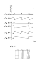
- the following describes the operation of the image correction apparatus shown in Fig. 1 including the convergence correction apparatus of the first embodiment with reference to the operation waveforms as shown in Figs. 2(a) to 2(f) and an image picture displayed on the display screen as shown in Fig. 3.
- the input terminal 2 receives two kinds of sync signals having different scanning frequencies from each other as shown in Figs. 2(a) and 2(c) alternatively and one of the input sync signals is supplied to the scanning waveform generating section 6.
- the amplitude control section 7 controls a power voltage (not shown) for driving the scanning waveform generating section 6 according to the scanning frequency of the scanning signal with receipt of the control signal so that the scanning waveform generating section 6 generates a regular deflection current of a sawtooth waveform having a regular amplitude as shown in Figs. 2(b) and 2(d).
- the sawtooth waveform generated by the scanning waveform generating section 6 is supplied to the deflection yoke 10.
- the control signal applied through the input terminal 3 is fed to a reference voltage terminal of a comparator (which is referred later with reference to Fig. 8) provided in the convergence correction waveform generating section 5, thereby allowing to set the raster size according to the control signal.
- a comparator which is referred later with reference to Fig. 8
- the control signal input through the terminal 3 is applied to the convergence correction waveform generating section 5 for setting the raster size while another output signal of the scanning waveform generating section 6 which is formed according to the scanning frequency of the input sync signal is also applied to the convergence correction waveform generating section 5, whereby the section 5 forms convergence correction waveforms of sawtooth shapes each having a regular amplitude as shown in Figs. 2(e) and 2(f) corresponding to the scanning frequencies and the raster size.
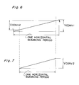
- a sawtooth waveform having an amplitude V CONV1 as shown in Fig. 6 is generated when the aspect ratio is 16 : 9 (H-SIZE 1 in Fig. 4), where the amplitude of the sawtooth waveform is linearly increased from zero to V CONV1 in one horizontal scanning period.
- the aspect ratio is 12 : 9 (H-SIZE 2 in Fig. 4)
- a sawtooth waveform having an amplitude V CONV2 as shown in Fig. 7 is generated, where the amplitude of the sawtooth waveform is linearly increased from zero to V coNV2 in one horizontal scanning period.
- Each of the above-mentioned convergence correction waveform signals is used for driving the convergence yoke 9 to perform the convergence correction.
- the correction waveform having the aspect ratio of 12: 9 (H-SIZE 2) as indicated by the dotted line in Fig. 4 is automatically formed based on the convergence correction data adjusted at the aspect ratio of 16 : 9 (H-SIZE 1) as indicated by the solid line in Fig. 4. Therefore, a good convergence image picture can be achieved on the display screen even when the aspect ratio is varied.
- Fig. 10(a) shows a constitution of a sawtooth waveform generating circuit composed of a mirror integration circuit
- Fig. 10(b) shows a chart of a waveform for explaining the operation of the integration circuit shown in Fig. 10(a)
- Fig.10(c) shows an equivalent circuit corresponding to the integration circuit shown in Fig. 10(a).
- an amplifier 107 has its input impedance being infinite (oo) and its output impedance being O
- current i flowing through a resistor 103 is entirely supplied to a capacitor 104. Therefore, the following equations (1) to (3) are obtained: when eliminating v o and v o from Equations (1) through (3), obtained is Equation (4) as following:
- the circuit constitution shown in Fig. 10(a) can be represented by the equivalent circuit shown in Fig. 10(c).
- the capacitance C is made (1-G) times in appearance.
- the circuit of Fig. 10(c) is an RC integration circuit, the integration time constant ⁇ m is given by:
- Equation (6) When G is -oo, im becomes 00 . Even when G is not -oo but sufficiently large negative value (i.e., considerable ⁇ m>t), the value of e in Fig. 10(c) is Vc (E/ ⁇ ) ⁇ t, where ⁇ is replaced by ⁇ m to obtain Equation (6) as following:
- the output v o is represented by the waveform shown in Fig. 10(b), which is represented by: where the equation represents formation of a sawtooth waveform. It is noted here from the above equation that the inclination of the output v o is due to the integration time constant ⁇ m.
- Fig. 11 shows an operational characteristic view between the input frequency and the output signal amplitude, where the amplitude increases in proportion to the square of the frequency as shown by a one-dotted broken line while a solid line represents an amplitude-regulated characteristic obtained through the feedback control loop which is described below in connection with Fig. 8.
- a fundamental correction waveform generating portion in the section 5 is composed of a plurality of feedback control loops 23 and 24 for automatic gain control and further feedback control loop (not shown) for higher-order correction arranged in parallel thereto.
- the first feedback control loop 23 for automatic gain control includes an integration circuit 14, amplitude detector circuit 15, comparator 16 and reference voltage generator circuit 18.
- the second feedback control loop 24 similarly includes an integration circuit 19, amplitude detector circuit 20, comparator 22 and reference voltage generator circuit 21.
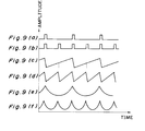
- an input terminal 11 receives scanning signals having different scanning frequencies as shown in Figs. 9(a) and 9(b), which the scanning waveforms correspond to the scanning output from the scanning waveform generating section 6.
- the input scanning signal supplied from the input terminal 11 is fed to the integration circuit 14 to generate a corresponding one of the sawtooth waveforms as shown in Figs. 9(c) and 9(d).
- the resulting sawtooth waveform output from the integration circuit 14 is fed back to the comparator 16 by way of the amplitude detector circuit 15.
- the amplitude of the sawtooth waveform output from the integration circuit 14 is detected by the amplitude detector circuit 15, and the resultant detection signal is compared by means of the comparator 16 with a reference voltage supplied from the reference voltage generator circuit 18 while the reference voltage is being added with the control signal by way of an adder 17.
- the adder 17 adds the control signal fed through the terminal 3 to the reference voltage.
- the resultant comparison signal output from the comparator 16 is fed back to a gain control terminal T G1 of the integration circuit 14 thereby to output a sawtooth waveform having a regular amplitude through an output terminal 12 even when the scanning frequency is changed as shown in Figs. 9(c) and 9(d).
- the sawtooth waveform output from the integration circuit 14 may have a different scanning frequency and a regular amplitude as shown in Figs. 9(c) and 9(d).
- the sawtooth waveform output from the integration circuit 14 having different scanning frequency and a regular amplitude is supplied to the integration circuit 19 in the second feedback control loop 24 to generate parabola waveforms as shown in Figs. 9(e) and 9(f) through another output terminal 13.
- the parabola waveform output from the integration circuit 19 is fed back to the amplitude detector circuit 20.
- the amplitude detector circuit 20 detects the amplitude of the parabola waveform, and the resultant detection signal is compared in the comparator 22 with a reference voltage supplied from the reference voltage generator circuit 21.
- the resultant comparison signal output from the comparator 22 is fed back to a gain control terminal T G2 of the integration circuit 19 to output a parabola waveform having a regular amplitude as shown in Figs. 9(e) and 9(f) through the output terminal 13 even when the scanning frequency is changed.
- the comparator 16 As a reference voltage applied to the comparator 16 in the first feedback control loop 23, the comparator 16 is supplied with a signal formed by adding the reference voltage generated by the reference voltage generator circuit 18 to the control signal for controlling the amplitude fed from the input terminal 3 in the adder 17. This means that the control signal fed through the input terminal 3 to the loop 23 changes the amplitudes of the convergence correction waveforms (sawtooth waveform and parabola waveform).
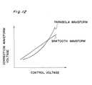
- Fig. 12 shows a relation between the control signal and each correction waveform voltage, where the amplitude of the correction waveform is controlled so that the amplitude of the sawtooth waveform is proportional to that of the control signal while the amplitude of the parabola waveform is proportional to the square of that of the control signal.
- the sawtooth and parabola waveforms each having a regular amplitude can be generated as the convergence correction waveforms even when the scanning frequency is changed, where in the first feedback control loop 23 the reference voltage is controlled by the control signal to form the sawtooth waveforms each having a regular amplitude proportional to that of the control signal.
- the resultant sawtooth waveforms are input to the second feedback control loop 24 to be further processed in the integration circuit 19, thereby automatically obtaining the parabola waveforms each having a regular amplitude proportional to the square of that of the control signal.
- a correction waveform in the vertical scanning period can be formed. Therefore, as described with regard to the correspondence in aspect ratio in conjunction with Figs. 4 through 7, a convergence correction waveform corresponding to each aspect ratio is automatically formed only by changing the control signal.
- Figs. 13(1) through 13(4) show variations in correction represented by the movement of display on the screen according to various convergence correction waveforms.
- Figs. 13(1-A) to 13(1-C) when a correction waveform of a vertical sawtooth waveform shown in Fig. 13(1-A) is supplied to a vertical convergence coil, vertical amplitude correction is performed as shown in Fig. 13(1-B), and on the other hand, when the correction waveform of the vertical sawtooth waveform is supplied to a horizontal convergence coil, orthogonal correction of vertical lines is performed as shown in Fig. 13(1-C).
- Figs. 13(2-A) to 13(2-C) when a correction waveform of a vertical parabola waveform shown in Fig. 13(2-A) is supplied to a vertical convergence coil, vertical linearity correction is performed as shown in Fig. 13(2-B), and on the other hand, when the correction waveform of the vertical parabola waveform is supplied to a horizontal convergence coil, vertical line curve correction is performed as shown in Fig. 13(2-C).
- Figs. 13(3-A) to 13(3-C) when a correction waveform of a horizontal sawtooth waveform shown in Fig. 13(3-A) is supplied to a vertical convergence coil, orthogonal correction of horizontal lines is performed as shown in Fig. 13(3-B), and on the other hand, when the correction waveform of the horizontal sawtooth waveform is supplied to a horizontal convergence coil, horizontal amplitude correction is performed as shown in Fig. 13(3-C).
- Figs. 13(4-A) to 13(4-C) when a correction waveform of a horizontal parabola waveform shown in Fig. 13(4-A) is supplied to a vertical convergence coil, horizontal line curve correction is performed as shown in Fig. 13(4-B), and on the other hand, when the correction waveform of the horizontal parabola waveform is supplied to a horizontal convergence coil, horizontal linearity correction is performed as shown in Fig. 13(4-C).
- the automatic convergence correction can be effected even when the scanning frequency and/or the aspect ratio is changed.
- Fig. 14 shows a divisional correction waveform generating portion of the section 5, which includes a horizontal (H) sawtooth waveform generator circuit 29, a horizontal (H) parabola waveform generator circuit 30, a horizontal (H) sine waveform generator circuit 31, a vertical (V) sawtooth waveform generator circuit 34, a vertical (V) parabola waveform generator circuit 35, and a vertical (V) sine waveform generator circuit 37, where each of the circuits is a correction waveform generator circuit composed of an integration circuit in the feedback control loop as shown in Fig. 8.
- the horizontal (H) sawtooth waveform generator circuit 29, horizontal (H) parabola waveform generator circuit 30, and horizontal (H) sine waveform generator circuit 31 are serially connected.
- the vertical (V) sawtooth waveform generator circuit 34, vertical (V) parabola waveform generator circuit 35, and vertical (V) sine waveform generator circuit 37 are serially connected.
- the horizontal (H) sawtooth waveform generator circuit 29 and vertical (V) sawtooth waveform generator circuit 34 correspond to the first feedback control loop 23 for automatic sawtooth waveform gain control shown in Fig. 8.
- the horizontal (H) parabola waveform generator circuit 30 and vertical (V) parabola waveform generator circuit 35 correspond to the second feedback control loop 24 for automatic parabola waveform gain control shown in Fig. 8.
- the horizontal (H) sine waveform generator circuit 31 and vertical (V) sine waveform generator circuit 37 correspond to further feedback control loop for higher-order correction for automatic sine waveform gain control (not shown in Fig. 8).
- the amplitude of the sawtooth waveform is proportional to that of the control signal
- the amplitude of the parabola waveform is proportional to the square of that of the control signal
- the amplitude of the sine waveform is proportional to the cube of that of the control signal.
- a horizontal scanning signal as shown in Fig. 15(a) input through the input terminal 25 is supplied to the H sawtooth waveform generator circuit 29 to form a horizontal sawtooth waveform as shown in Fig. 15(b) by receiving a horizontal amplitude control signal from a terminal 26.
- the sawtooth waveform generated by the H sawtooth waveform generator circuit 29 is supplied to the H parabola waveform generator circuit 30 to form a horizontal parabola waveform as shown in Fig. 15(c).
- the parabola waveform generated by the H parabola waveform generator circuit 30 is supplied to the H sine waveform generator circuit 31 to form a sine waveform as shown in Fig. 15(d).
- the sawtooth waveform generated by the H sawtooth waveform generator circuit 29 is also supplied to a comparator 32 to be compared with a reference voltage of 0 V for detecting the scanning center position of the sawtooth waveform to output a horizontal changeover signal as shown in Fig. 15(e).
- the horizontal changeover signal is supplied from the comparator 32 to a changeover circuit (SW) 33 to form horizontal (H) sine divisional correction waveforms 1 as shown in Figs. 15(f) and 15(g) at an output terminal 40.
- a vertical scanning signal as shown in Fig. 15(h) input through the input terminal 27 is supplied to the V sawtooth waveform generator circuit 34 to form a vertical sawtooth waveform as shown in Fig. 15(i) by receiving a vertical amplitude control signal from a terminal 28.
- the sawtooth waveform is supplied from the V sawtooth waveform generator circuit 34 to the V parabola waveform generator circuit 35 to form a vertical parabola waveform as shown in Fig. 150).
- the parabola waveform generated by the V parabola waveform generator circuit 35 is supplied to the V sine waveform generator circuit 37 to form a sine waveform as shown in Fig. 15(k).
- the sawtooth waveform generated by the V sawtooth waveform generator circuit 34 is also supplied to a comparator 36 to be compared with a reference voltage of 0 V for detecting the scanning center position of the sawtooth waveform to output a vertical changeover signal as shown in Fig. 15(1).
- the vertical changeover signal output from the comparator 36 is supplied to a changeover circuit (SW) 39 to form vertical (V) sine divisional correction waveforms 3 as shown in Figs. 15(m) and 15(n).
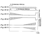
- an H sawtooth waveform from the H sawtooth waveform generator circuit 29 a V sawtooth waveform from the V sawtooth waveform generator circuit 34, and H and V changeover signals output from the comparators 32 and 36 respectively are supplied to further another changeover circuit (SW) 38 to form divisional correction waveforms 2 as shown in Figs. 16(c), 16(d), 16(e), and 16(f) at an output terminal 41 each having a horizontal scanning period shown in Fig. 16(a) and a vertical scanning period shown in Fig. 16(b).
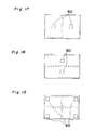
- Figs. 17 through 19 show division areas where the convergence is varied on the screen by the divisional correction waveforms.
- the divisional correction waveforms 1 shown in Figs. 15(f) and 15(g) can correct the convergence in areas divided right and left horizontally on the screen as shown in Fig. 17.
- the divisional correction waveforms 3 shown in Figs. 15(m) and 15(n) can correct the convergence in areas divided upper and lower vertically on the screen as shown in Fig. 18.
- the divisional correction waveforms 2 shown in Figs. 16(c) to 16(f) can correct the convergence at the four corners of the screen as shown in Fig. 19, where the left upper corner corresponds to the divisional correction waveform shown in Fig.
- each mark D 60 indicates a portion where the maximum change of convergence is effected.
- a high-accuracy convergence correction can be achieved by forming not only the fundamental correction waveforms but also the divisional correction waveforms as convergence correction waveforms.
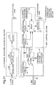
- Figs. 20 and 21 show constructions of a horizontal and vertical correction systems respectively. It is noted here that like parts in Figs. 20 and 21 similar to those in Fig. 8 are designated by the same reference numerals.
- a horizontal sync signal is applied to horizontal oscillator circuit 56 through a sync input terminal 2, which the oscillator circuit 56 performs a pulse oscillation in synchronization with the sync signal.
- the output of the oscillator circuit 56 is applied to a horizontal drive circuit 57 which performs a drive operation for driving the horizontal output signal.
- the output of the drive circuit 57 is applied to a horizontal output circuit 58 which drives a deflection york 10 to effect a horizontal scanning with horizontal deflection current of a sawtooth waveform flowing therethrough, where the circuits 56, 57 and 58 are included in the section 6.
- a flyback pulse is induced by the deflection york 10 and the peak value of the pulse is detected by a peak value detector 62 and the resultant detection value is supplied to a comparator 60.
- the comparator 60 compares the detection peak value with a reference voltage supplied from a reference voltage generating circuit 61 by way of an adder 17'.
- the comparison result output from the comparator 60 applied to a power voltage control circuit 59, where the circuits 59 through 62 are included in the section 7.
- the power voltage control circuit 59 controls the source voltage to be supplied to the horizontal output circuit 58 in such a manner that the flyback pulse has a constant peak value.
- the flyback pulse induced in the deflection york 10 is supplied to a two-value circuit 63 in the section 6 to form a horizontal scanning signal for forming a fundamental correction waveform for convergence correction.
- the horizontal scanning signal output from the two-value circuit 63 is supplied to a feedback control loop comprised of an integration circuit 14, amplitude detector circuit 15, comparator 16, adder 17 and reference voltage generating circuit 18 provided in the section 5 as described in connection with Fig. 8, thereby forming a horizontal sawtooth waveform.
- an integration circuit 19 generates a horizontal parabola waveform
- the subsequent integration circuit 64 generates a horizontal sine waveform
- a division waveform generating circuit 65 generates a division correction waveform.
- the correction waveforms output from the integration circuits 14, 19 and 64 and the division waveform generating circuit 65 are supplied to an adder 66 to be added together. Thereafter, the output of the adder 66 is amplified by means of an amplifier 67 to drive the convergence york 9 through which a horizontal convergence correction current flows to perform the horizontal convergence correction.
- the horizontal amplitude control signal applied through the input terminal 26 is supplied to the scanning waveform generating section 6 and to the adder 17' located in the amplitude control section 7.
- the horizontal amplitude control signal is also applied to the adder 17 in the feedback control loop in the convergence correction waveform generating section 5, thereby controlling the raster size and forming a convergence correction corresponding to the raster size.
- a vertical sync signal is applied to a vertical oscillator circuit 68 through the input terminal 2 to perform a pulse oscillation in synchronization with the sync signal.
- the output from the oscillator circuit 68 is applied to a two-value circuit 69 to form a binary data to form a vertical scanning signal for forming a fundamental correction waveform for convergence correction.
- the vertical scanning signal output from the two-value circuit 69 is supplied to a feedback control loop comprised of an integration circuit 14, amplitude detector circuit 15, comparator 16, adder 17 and reference voltage generating circuit 18 provided in the section 5 as described in connection with Fig. 8, thereby forming a vertical sawtooth waveform.
- an integration circuit 19 generates a vertical parabola waveform
- the subsequent integration circuit 64 generates a vertical sine waveform
- a division waveform generating circuit 65 generates a division correction waveform.
- the correction waveforms output from the integration circuits 14, 19 and 64 and the division waveform generating circuit 65 are supplied to an adder66 to be added together. Thereafter, the output of the adder 66 is amplified by means of an amplifier 67 to drive the convergence york 9 through which a vertical convergence correction current flows to perform the vertical convergence correction.
- the vertical amplitude control signal applied through the input terminal 28 is supplied to the adder 17 in the feedback control loop in the convergence correction waveform generating section 5, thereby controlling the raster size and forming a convergence correction corresponding to the raster size.
- the vertical sawtooth waveform output from the integration circuit 14 is supplied to a vertical output circuit 70 to drive the deflection york 10 through which vertical deflection current of a sawtooth waveform flows to perform the vertical scanning operation.
- the scanning signal of a vertical sawtooth waveform is used in common both the scanning waveform generating section 6 and the convergence correction waveform generating section 5. Therefore, a stable amplitude control is performed, flowing a constant deflection current through the deflection york 10 to maintain the vertical amplitude to be constant.
- the vertical output circuit 70 receives the vertical sawtooth waveform signal output from the feedback control loop composed of the integration circuit 14 and the like in the section 5 as its input signal, there may be provided a similar feedback control loop between the vertical oscillator circuit 68 and the vertical output circuit 70 to generate a vertical scanning waveform.
- a convergence correction waveform is formed in accordance with the scanning waveform corresponding to the scanning frequency and the raster size, so that a convergence correction can be effected automatically following the signal sources having different scanning frequencies and different aspect ratios, which remarkably reduces the time for adjustment.
- Fig. 22 shows an image correction apparatus which includes a convergence correction apparatus in accordance with a second embodiment of the present invention.
- the convergence correction apparatus includes a fundamental correction waveform generation section 43 for forming a fundamental correction waveform for convergence correction according to the sync signal input through the input terminal 2 and the control signal input through the input terminal 3 for controlling the raster size.
- the convergence correction apparatus further includes a memory 44 for storing correction data for controlling the amplitude of each fundamental correction waveform.
- the apparatus also includes a multiplication type digital-to-analog converter 45 (referred to as "multiplication type D-A converter” hereinafter) having a digital-to-analog conversion function for converting digital correction data supplied from the memory 44 into an analog quantity and a multiplication function for multiplying the resulting conversion signal by each correction waveform fed from the fundamental correction waveform generation section 43 to control the amplitude and direct current electric potential of the fundamental correction waveform.
- Reference numeral 46 denotes a convergence correction waveform generation section for generating a convergence correction waveform according to each amplitude-controlled fundamental correction waveform output from the multiplication type D-A converter 45. The convergence correction waveform output from the section 46 is supplied to the convergence york 9 to be driven.
- the scanning waveform generating section 6 receives the sync signal and the control signal through the terminals 2 and 3 respectively to generates the scanning waveform signal corresponding to the scanning frequency which is fed to the fundamental correction waveform generation section 43 which generates an analog correction waveform of parabola and sawtooth waveform in each scanning direction.
- the analog correction waveform output from the section 43 is applied to the reference voltage input terminal of the multiplication type D-A converter 45.
- the control signal applied through the input terminal 3 is supplied to the fundamental correction waveform generating section 46 to control the reference voltage in the feedback control loop for forming the sawtooth waveform as described in connection with Fig. 14, thereby forming a fundamental correction waveform corresponding to the aspect ration.
- the correction data for each fundamental correction waveform is stored in the memory 44 and the digital correction data output from the memory 44 is supplied to a data input terminal of the multiplication type D-A converter 45.
- the multiplication type D-A converter 45 multiplies the digital-to-analog conversion signal by the analog fundamental correction waveform to control the amplitude of the correction waveform and direct current electric potential.
- the correction data output from the multiplication type D-A converter 45 is supplied to the convergence correction waveform generation section 46 to form a correction waveform for driving the convergence yoke 9.
- the scanning signal output from the scanning waveform generating section 6 and the control signal are both supplied to the fundamental correction waveform generating section 43 by way of the input terminals 11 and 3 respectively to form a fundamental correction waveform corresponding to the scanning frequency and the raster size.
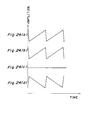
- the serial correction data output from the memory 44 is input to the D/A converter 49 by way of an input terminal 47 shown in Fig. 23.
- a horizontal sawtooth waveform as shown in Fig. 24 (a) is supplied from the fundamental correction waveform generation section 43 to the D/A converter 49 by way of a reference voltage terminal 48.
- a multiplication type D-Aconverter49 an analog data obtained through a digital-to-analog conversion of the serial digital data input through the input terminal 47 is multiplied by an analog correction waveform input through the reference voltage terminal 48.
- the relation between the memory data of 16 scale system of notation (i.e., total 256 steps of data) output from the memory 44 and the correction waveform output from the section 43 is shown in Table 1.
- Fig. 24 (b) when the data of 16-scale notation from the memory 44 is the minimum value of OOH (i.e., 000), or generated is an uncorrected flat correction waveform without signal representation as shown in Fig. 24 (c) when the data from the memory 44 is the middle value of 80H (i.e., 128), or generated is an output correction waveform with a negative polarity as shown in Fig. 24 (d) when the data from the memory 44 is the maximum value of FFH (i.e., 256).
- OOH i.e., 000
- Fig. 24 (c) when the data from the memory 44 is the middle value of 80H (i.e., 128)
- Fig. 24 (d) when the data from the memory 44 is the maximum value of FFH (i.e., 256).
- the above fact means that the amplitude and the polarity of the correction waveform is controlled in accordance with the data from the memory 44. Therefore, it is possible to form an optimum correction waveform for each portion to be corrected.
- the correction waveforms and data output from the multiplication type D-A converters 49 through 53 are supplied to an adder 54 which forms a convergence correction waveform for effecting convergence correction by adding fundamental correction waveforms necessary for various correction systems.
- a convergence correction waveform is formed from the scanning waveform corresponding to the scanning frequency and the raster size.
- the apparatus of the present embodiment can automatically form an optimum convergence correction waveform even for the signal sources having different scanning frequencies and different aspect ratios by merely writing one type of fundamental correction data into the memory 44.
- various control signals such as remote control code signals are supplied to a microprocessor (CPU) 75 by way of an input terminal 77 for controlling the convergence correction and raster size, and the microprocessor 75 judges the remote control code signals to store the correction data in the memory 44 for various corrections.
- the correction data output from the memory 44 is supplied to both the multiplication type D/A converter 45 for convergence correction and anot her D/A converter 76 for controlling raster size.
- the D/A converter 45 is operated in the same manner as described above.
- the control signal output from the raster size D/A converter 76 is fed back to both the section 6 and the section 43 to form the scanning waveform and convergence correction waveform corresponding to the raster size.
- the scanning waveform generating section has the same construction as that of the first embodiment shown in Figs. 20 and 21, which is remarkably effective in the digital control system using the D/A converters and memory.
- the present invention as described above, by digitally forming a convergence correction waveform according to a scanning waveform corresponding to a scanning frequency and a raster size, reduction of the circuit scale and stabilization of the correction waveform can be assured thereby remarkably reducing the time for adjustment by virtue of the automatized adjustment arrangement. Furthermore, the data line amount can be remarkably reduced by using a serial input type digital-to-analog converter.
- each sawtooth waveform may be formed as a correction waveform from the scanning waveform generation means.
- each correction waveform is added in analog form in the second embodiment, the addition may be effected digitally.
- a convergence correction waveform is formed in accordance with the scanning frequency and the raster size so that the convergence can be corrected automatically following signal sources having different scanning frequencies and different aspect ratios thereby to allow a remarkable reduction of the adjustment time to be achieved.
- a correction waveform in a manner that the sawtooth waveform is proportional in amplitude to the control signal and the parabola waveform is proportional in amplitude to the square of the control signal, a high-accuracy convergence correction can be achieved even for a signal source having a different aspect ratio.
- the first inventive apparatus by detecting the scanning center position from a sawtooth waveform and forming divisional correction waveforms for the upper, lower, right, left, and four corner portions of the screen according to the detection signal, an improved correction accuracy can be achieved in the peripheral areas of the screen.
- the second inventive apparatus by digitally forming a convergence correction waveform from the scanning waveform corresponding to the scanning frequency and the rastersize, an automatic adjustment can be achieved together with reduction of the circuit scale and stabilization of the correction waveforms to allow a remarkable reduction of the time for adjustment.
- the data line amount can be remarkably reduced.
Abstract
Description
- The present invention relates to a convergence correction apparatus for use in a color television receiver, and more particularly to a convergence correction apparatus capable of performing an automatic convergence correction with high accuracy by digitally controlling various correction waveforms.
- Generally in a video projector, three projection tubes are used for applying light beams of three primary colors red (R), green (G) and blue (B) for expanding and projecting a video image picture onto a screen, where the incident projection angles (hereinafter, referred to as, "convergence angle") of the light beams from the projection tubes with respect to the screen are different from each other, resulting in that color deviation, i.e., misconvergence may occur in the picture displayed on the screen. Convergence correction to such misconvergence has been implemented by such a system that an analog-like correction waveform is created in synchronization with horizontal and vertical scanning periods so that the amplitude and shape af the analog-like correction waveform are varied to be adjusted for the convergence correction. However, such a conventional system has been accompanied by a problem in the viewpoint of correction accuracy.
- The conventional adjustment system mentioned above has been also accompanied by another problem that much time is required in operation because the correction is manually performed while visually observing the misconvergence on the screen.
- In order to solve this problem, the Japanese Patent Unexamined Laid-Open No. 8114/1984 discloses a digital convergence apparatus capable of convergence correction with high accuracy. Besides, the Japanese Patent Publication No. 38797/1991 discloses a digital convergence apparatus for performing an automatic correction. The Japanese Patent Publication No. 5314/1992 discloses a digital convergence apparatus capable of coping with various scanning frequencies. The Japanese Patent Unexamined Laid-Open No. 11388/1987 discloses a digital convergence apparatus capable of coping with various aspect ratios. The Japanese Patent Unexamined Laid-Open Nos. 122417/1977, 147016/1977, and 79893/1985 each discloses a method of performing a convergence correction by dividing an analog waveform.
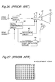
- One of such conventional convergence correction apparatuses for use in a video projector is described below with reference to Fig. 21.
- Referring to Fig. 21, the apparatus includes a projection cathode-
ray tube 8, aconvergence yoke 9, adeflection yoke 10, ascreen 86, and aprojection lens 87. - A video signal is applied to a
video circuit 81 through avideo input terminal 1, where the input video signal is amplified to an appropriate amplitude to drive the projection cathode-ray tube 8. Thevideo circuit 81 serves as the conventional television receiver in the normal mode, whereas it displays, as shown in Fig. 22, on the display screen a crosshatch signal fed from adigital convergence circuit 82 during a convergence adjustment operation mode. - In the digital convergence of the crosshatch signal, correction data of adjustment points displayed on the screen is stored and interpolation of the correction data is performed among the adjustment points to create a correction waveform. Accordingly, correction can be effected for each adjustment point independently, so that high-accuracy correction can be implemented. Electron beams are scanned by means of a
deflection circuit 83 and thedeflection yoke 10 in the projection cathode-ray tube 8 in accordance with a sync. signal applied through a sync.signal input terminal 2. Although a single projection cathode-ray tube 8 is shown in Fig. 21, normally used are three projection cathode-ray tubes for primary three colors of R, G and B. - An
adjustment pattern detector 85 such as a camera performing photodetection, detects a crosshatch pattern projected on thescreen 86. The detection signal of the crosshatch pattern is fed from thedetector 85 to an adjustment-point detector circuit 84. The adjustment-point detector circuit 84 detects convergence deviation of each adjustment point and adjusts the amount of correction of thedigital convergence circuit 82 according to the resultant detection signal, thus automatically accomplishing the convergence adjustment. - As described above, by detecting the misconvergence in the picture displayed on the screen with the
detector camera 85 and using the resulting detection signal to control correction data, there can be achieved an automatically adjustable high-accuracy convergence correction apparatus. - In such a conventional convergence correction apparatus as described above, it is required to input misconvergence correction data of each adjustment point in each mode in order to cope with signal sources having different input scanning frequencies and different aspect ratios. Therefore, the conventional apparatus has such problems that it requires much time for the adjustment and significantly increased memory capacity and circuit scale due to the necessity of a particular adjustment function for each mode.
- According to a first aspect of this invention a convergence correction apparatus comprises: scanning waveform generating means for generating a scanning waveform with receipt of a sync signal for scanning an electron beam in a cathode ray tube; control means for controlling a raster size according to the scanning waveform generated by said scanning waveform generating means with receipt of a control signal; and correction waveform generating means for generating a correction waveform for performing a convergence correction according to the scanning waveform and the control signal, whereby convergence correction is formed in accordance with the scanning waveform corresponding to the scanning frequency and the raster size.
- According to a first feature of the present invention, the apparatus can automatically follow convergence correction signal sources having different input scanning frequencies and different aspect ratios, thereby remarkably reducing the time necessary for the adjustment.
- According to a second aspect of this invention a convergence correction apparatus comprises: control means for controlling a raster size defined by a scanning waveform according to a control signal; fundamental correction waveform generating means for generating a fundamental correction waveform for correcting a convergence according to the scanning waveform and the control signal; memory means for storing amplitude-control data for amplitude-controlling the fundamental correction waveform; conversion means for a multiplication type digital-to-analog conversion of the amplitude-control data and the fundamental correction waveform; and correction waveform generation means for generating a correction waveform for performing convergence correction according to the resulting conversion signal, thereby digitally forming convergence correction data according to the scanning waveform corresponding to the scanning frequency and the raster size.
- According to a second feature of the present invention, the apparatus can effect a stable high-accuracy convergence correction to easily achieve an automatic adjustment.
- Particular embodiments of the present invention will now be described with reference to the accompanying drawings, in which:
- Fig. 1 is a block diagram showing an image correction apparatus including a convergence correction apparatus in accordance with a first embodiment of the present invention;
- Figs. 2(a), 2(b), 2(c), 2(d), 2(e) and 2(f) are charts of waveforms for explaining the operation of the first embodiment with respect to a scanning frequency;
- Fig. 3 is a view of a display screen for explaining the operation of the first embodiment with respect to a scanning frequency;
- Fig. 4 is a view of a display screen for explaining an operation of the first embodiment with respect to an aspect ratio;
- Fig. 5 is a graph showing a relation between a horizontal size (H size) and a control voltage for controlling the raster size;
- Fig. 6 is a chart of a waveform for explaining an operation of the first embodiment with respect to an aspect ratio;
- Fig. 7 is a chart of a waveform for explaining an operation of the first embodiment with respect to an aspect ratio;
- Fig. 8 is a block diagram of the fundamental correction waveform generation section of the first embodiment;
- Figs. 9(a), 9(b), 9(c), 9(d), 9(e), and 9(f) are charts of waveforms for explaining the operation of the fundamental correction waveform generation section of the first embodiment;
- Fig. 10(a) is a circuit arrangement for explaining a sawtooth waveform generating section composed of a mirror integration circuit according to the present invention;
- Figs. 1 0(b-1) and 10(b-2) are charts each for explaining an operational waveform of the circuit arrangement of Fig. 10(a);
- Fig. 10(c) is a diagram showing an equivalent circuit of fig. 10(a);
- Fig. 11 is a graph showing an operational characteristic between the input frequency and the output signal amplitude of the circuit of Fig. 10(a);
- Fig. 12 is a graph showing a relation between a control voltage and each correction waveform voltage;
- Figs. 13(1-A), 13(1-B), 13(1-C); 13(2-A), 13(2-B), 13(2-C); 13(3-A), 13(3-B), 13(3-C); and 13(4-A), 13(4-B), 13(4-C) are schematic diagrams each showing correction variations with respect to correction waveforms of the first embodiment;
- Fig. 14 is a block diagram of a divisional correction waveform generation section of the first embodiment;
- Figs. 15(a), 15(b), 15(c), 15(d), 15(e), 15(f), 15(g), 15(h), 15(i), 150),15(k), 15(l), 15(m), and 15(n)are charts of waveforms for explaining the operation of the divisional correction waveform generation section of the first embodiment;
- Figs. 16(a), 16(b), 16(c), 16(d), 16(e) and 16(f) are charts of waveforms for explaining the operation of the divisional correction waveform generation section of the first embodiment;
- Fig. 17 is a view of a display screen for explaining the operation of the divisional correction waveform generation section of the first embodiment;
- Fig. 18 is a view of another display screen for explaining the operation of the divisional correction waveform generation section of the first embodiment;
- Fig. 19 is a view of yet another display screen for explaining the operation of the divisional correction waveform generation section of the first embodiment;
- Figs. 20 and 21 are block diagrams showing constructions of a horizontal and vertical correction systems respectively;
- Fig. 22 is a block diagram of an image correction apparatus including a convergence correction apparatus in accordance with a second embodiment of the present invention;
- Fig. 23 is a block diagram of a data control system of the second embodiment;
- Figs. 24(a), 24(b), 24(c) and 24(d) are charts of waveforms for explaining the operation of the data control system of the second embodiment;
- Fig. 25 is a block diagram for explaining the scanning waveform generation and convergence correction waveform generation;
- Fig. 26 is a block diagram of a conventional convergence correction apparatus; and
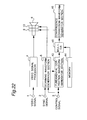
- Fig. 27 is a view of a display screen on which a cross hatching signal is displayed in the conventional apparatus.
- The following describes preferred embodiments of the present invention with reference to the attached drawings. Before the description proceeds, it is to be noted here that similar parts are designated by the same reference numerals throughout the drawings.
- Fig. 1 shows a block diagram of an image correction apparatus which includes a convergence correction apparatus in accordance with a first embodiment of the present invention.
- Referring to Fig. 1, a video signal is input to a video signal processing section 4 through a video
signal input terminal 1. The convergence correction apparatus is provided with a syncsignal input terminal 2 for receiving a sync signal, and a controlsignal input terminal 3 for receiving a control signal for controlling a raster size according to various aspect ratios. The video signal processing section 4 amplifies the input video signal to a level required for driving acathode ray tube 8. Thecathode ray tube 8 is provided with aconvergence yoke 9 and adeflection yoke 10. - The apparatus includes a convergence correction
waveform generating section 5 for generating a convergence correction waveform for driving theconvergence yoke 9 and further includes a scanningwaveform generating section 6 for generating a scanning waveform for driving thedeflection yoke 10. In thesection 6, the scanning waveform is formed in synchronization with the sync signal applied through theinput terminal 2 thereby to drive thedeflection yoke 10. The convergence correctionwaveform generating section 5 receives the control signal applied through theinput terminal 3 and the scanning waveform output from the scanningwaveform generating section 6 so that thesection 5 generates the convergence correction waveform according to the control signal and the scanning waveform to drive theconvergence yoke 9.Reference numeral 7 denotes an amplitude control section which also receives the control signal entered through theinput terminal 3 and the scanning waveform output from the scanningwaveform generating section 6. The output signal of thesection 7 is applied to the scanningwaveform generating section 6 performing a feedback-control to have a regular raster size even when various signal sources having different scanning frequencies are used. - The following describes the operation of the image correction apparatus shown in Fig. 1 including the convergence correction apparatus of the first embodiment with reference to the operation waveforms as shown in Figs. 2(a) to 2(f) and an image picture displayed on the display screen as shown in Fig. 3.
- The
input terminal 2 receives two kinds of sync signals having different scanning frequencies from each other as shown in Figs. 2(a) and 2(c) alternatively and one of the input sync signals is supplied to the scanningwaveform generating section 6. Theamplitude control section 7 controls a power voltage (not shown) for driving the scanningwaveform generating section 6 according to the scanning frequency of the scanning signal with receipt of the control signal so that the scanningwaveform generating section 6 generates a regular deflection current of a sawtooth waveform having a regular amplitude as shown in Figs. 2(b) and 2(d). The sawtooth waveform generated by the scanningwaveform generating section 6 is supplied to thedeflection yoke 10. The control signal applied through theinput terminal 3 is fed to a reference voltage terminal of a comparator (which is referred later with reference to Fig. 8) provided in the convergence correctionwaveform generating section 5, thereby allowing to set the raster size according to the control signal. - The control signal input through the
terminal 3 is applied to the convergence correctionwaveform generating section 5 for setting the raster size while another output signal of the scanningwaveform generating section 6 which is formed according to the scanning frequency of the input sync signal is also applied to the convergence correctionwaveform generating section 5, whereby thesection 5 forms convergence correction waveforms of sawtooth shapes each having a regular amplitude as shown in Figs. 2(e) and 2(f) corresponding to the scanning frequencies and the raster size. - Accordingly, even when the scanning frequency differs between the two sync signals as shown in Figs. 2(a) and 2(c), a correction waveform corresponding to the latter scanning frequency shown in Fig. 2(c) is automatically formed from the convergence correction data adjusted according to the former scanning frequency shown in Fig. 2(a). Therefore, a good convergence image display can be achieved on the display screen as shown by the cross hatching image picture in Fig. 3.
- The following describes an operation in a case where the aspect ratio is varied, with reference to Figs. 4, 5, 6 and 7.
- Referring to Figs. 4 and 5, when the aspect ratio is changed from 16 : 9 (H-
SIZE 1 as indicated by the solid line) to 4 : 3, i.e., 12 : 9 (H-SIZE 2 as indicated by the dotted line), the H-SIZE 1 corresponds to a control voltage VH1, while the H-SIZE 2 corresponds to a control voltage VH2 as shown in Fig. 5. Therefore, by inputting each of the above-mentioned control signals VH1 and VH2 to theinput terminal 3, the corresponding aspect ratio as shown in Fig. 4 can be set. - In regard to a correction waveform generated from the convergence correction
waveform generating section 5, a sawtooth waveform having an amplitude VCONV1 as shown in Fig. 6 is generated when the aspect ratio is 16 : 9 (H-SIZE 1 in Fig. 4), where the amplitude of the sawtooth waveform is linearly increased from zero to VCONV1 in one horizontal scanning period. When the aspect ratio is 12 : 9 (H-SIZE 2 in Fig. 4), a sawtooth waveform having an amplitude VCONV2 as shown in Fig. 7 is generated, where the amplitude of the sawtooth waveform is linearly increased from zero to VcoNV2 in one horizontal scanning period. Each of the above-mentioned convergence correction waveform signals is used for driving theconvergence yoke 9 to perform the convergence correction. The correction waveform having the aspect ratio of 12: 9 (H-SIZE 2) as indicated by the dotted line in Fig. 4 is automatically formed based on the convergence correction data adjusted at the aspect ratio of 16 : 9 (H-SIZE 1) as indicated by the solid line in Fig. 4. Therefore, a good convergence image picture can be achieved on the display screen even when the aspect ratio is varied. - The following describes a method of forming a fundamental correction waveform for convergence correction with reference to Fig. 8, Figs. 9(a) through 9(f), Figs. 10(a) through 10(c), and Fig. 11.
- In order to clearly understand the present invention, an operation of a integration circuit for forming various correction waveforms is first generally described below with reference to Figs. 10(a) through 10(c) and Fig. 11.
- Fig. 10(a) shows a constitution of a sawtooth waveform generating circuit composed of a mirror integration circuit, Fig. 10(b) shows a chart of a waveform for explaining the operation of the integration circuit shown in Fig. 10(a), and Fig.10(c) shows an equivalent circuit corresponding to the integration circuit shown in Fig. 10(a). Assuming that an
amplifier 107 has its input impedance being infinite (oo) and its output impedance being O, current i flowing through aresistor 103 is entirely supplied to acapacitor 104. Therefore, the following equations (1) to (3) are obtained:


when eliminating vo and vo from Equations (1) through (3), obtained is Equation (4) as following:
- Accordingly, the circuit constitution shown in Fig. 10(a) can be represented by the equivalent circuit shown in Fig. 10(c). In this arrangement having the
amplifier 107, the capacitance C is made (1-G) times in appearance. Since the circuit of Fig. 10(c) is an RC integration circuit, the integration time constant τm is given by:
- When G is -oo, im becomes 00. Even when G is not -oo but sufficiently large negative value (i.e., considerable τm>t), the value of e in Fig. 10(c) is Vc (E/τ)· t, where τ is replaced by τm to obtain Equation (6) as following:

- Accordingly, from Equations (2) and (6), the output vo is represented by the waveform shown in Fig. 10(b), which is represented by:

where the equation represents formation of a sawtooth waveform. It is noted here from the above equation that the inclination of the output vo is due to the integration time constant τm. - Fig. 11 shows an operational characteristic view between the input frequency and the output signal amplitude, where the amplitude increases in proportion to the square of the frequency as shown by a one-dotted broken line while a solid line represents an amplitude-regulated characteristic obtained through the feedback control loop which is described below in connection with Fig. 8.
- Referring to Fig. 8, a fundamental correction waveform generating portion in the
section 5 is composed of a plurality offeedback control loops feedback control loop 23 for automatic gain control includes anintegration circuit 14,amplitude detector circuit 15,comparator 16 and referencevoltage generator circuit 18. The secondfeedback control loop 24 similarly includes anintegration circuit 19,amplitude detector circuit 20,comparator 22 and referencevoltage generator circuit 21. - In the first
feedback control loop 23 for automatic gain control of a sawtooth waveform, aninput terminal 11 receives scanning signals having different scanning frequencies as shown in Figs. 9(a) and 9(b), which the scanning waveforms correspond to the scanning output from the scanningwaveform generating section 6. The input scanning signal supplied from theinput terminal 11 is fed to theintegration circuit 14 to generate a corresponding one of the sawtooth waveforms as shown in Figs. 9(c) and 9(d). The resulting sawtooth waveform output from theintegration circuit 14 is fed back to thecomparator 16 by way of theamplitude detector circuit 15. - The amplitude of the sawtooth waveform output from the
integration circuit 14 is detected by theamplitude detector circuit 15, and the resultant detection signal is compared by means of thecomparator 16 with a reference voltage supplied from the referencevoltage generator circuit 18 while the reference voltage is being added with the control signal by way of anadder 17. Theadder 17 adds the control signal fed through theterminal 3 to the reference voltage. The resultant comparison signal output from thecomparator 16 is fed back to a gain control terminal TG1 of theintegration circuit 14 thereby to output a sawtooth waveform having a regular amplitude through anoutput terminal 12 even when the scanning frequency is changed as shown in Figs. 9(c) and 9(d). The sawtooth waveform output from theintegration circuit 14 may have a different scanning frequency and a regular amplitude as shown in Figs. 9(c) and 9(d). - The sawtooth waveform output from the
integration circuit 14 having different scanning frequency and a regular amplitude is supplied to theintegration circuit 19 in the secondfeedback control loop 24 to generate parabola waveforms as shown in Figs. 9(e) and 9(f) through anotheroutput terminal 13. - In the second
feedback control loop 24 for automatic gain control of a parabola waveform, the parabola waveform output from theintegration circuit 19 is fed back to theamplitude detector circuit 20. Theamplitude detector circuit 20 detects the amplitude of the parabola waveform, and the resultant detection signal is compared in thecomparator 22 with a reference voltage supplied from the referencevoltage generator circuit 21. The resultant comparison signal output from thecomparator 22 is fed back to a gain control terminal TG2 of theintegration circuit 19 to output a parabola waveform having a regular amplitude as shown in Figs. 9(e) and 9(f) through theoutput terminal 13 even when the scanning frequency is changed. - As a reference voltage applied to the
comparator 16 in the firstfeedback control loop 23, thecomparator 16 is supplied with a signal formed by adding the reference voltage generated by the referencevoltage generator circuit 18 to the control signal for controlling the amplitude fed from theinput terminal 3 in theadder 17. This means that the control signal fed through theinput terminal 3 to theloop 23 changes the amplitudes of the convergence correction waveforms (sawtooth waveform and parabola waveform). - Fig. 12 shows a relation between the control signal and each correction waveform voltage, where the amplitude of the correction waveform is controlled so that the amplitude of the sawtooth waveform is proportional to that of the control signal while the amplitude of the parabola waveform is proportional to the square of that of the control signal.
- By the first and second
feedback control loop feedback control loop 23 the reference voltage is controlled by the control signal to form the sawtooth waveforms each having a regular amplitude proportional to that of the control signal. The resultant sawtooth waveforms are input to the secondfeedback control loop 24 to be further processed in theintegration circuit 19, thereby automatically obtaining the parabola waveforms each having a regular amplitude proportional to the square of that of the control signal. - In the same manner as the formation of the fundamental correction waveform in the horizontal scanning period as described above, a correction waveform in the vertical scanning period can be formed. Therefore, as described with regard to the correspondence in aspect ratio in conjunction with Figs. 4 through 7, a convergence correction waveform corresponding to each aspect ratio is automatically formed only by changing the control signal.
- Figs. 13(1) through 13(4) show variations in correction represented by the movement of display on the screen according to various convergence correction waveforms.
- Referring to Figs. 13(1-A) to 13(1-C), when a correction waveform of a vertical sawtooth waveform shown in Fig. 13(1-A) is supplied to a vertical convergence coil, vertical amplitude correction is performed as shown in Fig. 13(1-B), and on the other hand, when the correction waveform of the vertical sawtooth waveform is supplied to a horizontal convergence coil, orthogonal correction of vertical lines is performed as shown in Fig. 13(1-C).
- Referring to Figs. 13(2-A) to 13(2-C), when a correction waveform of a vertical parabola waveform shown in Fig. 13(2-A) is supplied to a vertical convergence coil, vertical linearity correction is performed as shown in Fig. 13(2-B), and on the other hand, when the correction waveform of the vertical parabola waveform is supplied to a horizontal convergence coil, vertical line curve correction is performed as shown in Fig. 13(2-C).
- Referring to Figs. 13(3-A) to 13(3-C), when a correction waveform of a horizontal sawtooth waveform shown in Fig. 13(3-A) is supplied to a vertical convergence coil, orthogonal correction of horizontal lines is performed as shown in Fig. 13(3-B), and on the other hand, when the correction waveform of the horizontal sawtooth waveform is supplied to a horizontal convergence coil, horizontal amplitude correction is performed as shown in Fig. 13(3-C).
- Referring to Figs. 13(4-A) to 13(4-C), when a correction waveform of a horizontal parabola waveform shown in Fig. 13(4-A) is supplied to a vertical convergence coil, horizontal line curve correction is performed as shown in Fig. 13(4-B), and on the other hand, when the correction waveform of the horizontal parabola waveform is supplied to a horizontal convergence coil, horizontal linearity correction is performed as shown in Fig. 13(4-C).
- As shown in Figs. 13(1) through 13(4), the automatic convergence correction can be effected even when the scanning frequency and/or the aspect ratio is changed.
- Then the following describes in detail a method for forming a divisional correction waveform with reference to Fig. 14 and Figs. 15(a) through 15(n).
- Fig. 14 shows a divisional correction waveform generating portion of the
section 5, which includes a horizontal (H) sawtoothwaveform generator circuit 29, a horizontal (H) parabolawaveform generator circuit 30, a horizontal (H) sinewaveform generator circuit 31, a vertical (V) sawtoothwaveform generator circuit 34, a vertical (V) parabolawaveform generator circuit 35, and a vertical (V) sinewaveform generator circuit 37, where each of the circuits is a correction waveform generator circuit composed of an integration circuit in the feedback control loop as shown in Fig. 8. The horizontal (H) sawtoothwaveform generator circuit 29, horizontal (H) parabolawaveform generator circuit 30, and horizontal (H) sinewaveform generator circuit 31 are serially connected. Also, the vertical (V) sawtoothwaveform generator circuit 34, vertical (V) parabolawaveform generator circuit 35, and vertical (V) sinewaveform generator circuit 37 are serially connected. The horizontal (H) sawtoothwaveform generator circuit 29 and vertical (V) sawtoothwaveform generator circuit 34 correspond to the firstfeedback control loop 23 for automatic sawtooth waveform gain control shown in Fig. 8. The horizontal (H) parabolawaveform generator circuit 30 and vertical (V) parabolawaveform generator circuit 35 correspond to the secondfeedback control loop 24 for automatic parabola waveform gain control shown in Fig. 8. The horizontal (H) sinewaveform generator circuit 31 and vertical (V) sinewaveform generator circuit 37 correspond to further feedback control loop for higher-order correction for automatic sine waveform gain control (not shown in Fig. 8). Regarding the relation between the amplitude of the respective waveforms and that of the control signal, the amplitude of the sawtooth waveform is proportional to that of the control signal, the amplitude of the parabola waveform is proportional to the square of that of the control signal, and the amplitude of the sine waveform is proportional to the cube of that of the control signal. - A horizontal scanning signal as shown in Fig. 15(a) input through the
input terminal 25 is supplied to the H sawtoothwaveform generator circuit 29 to form a horizontal sawtooth waveform as shown in Fig. 15(b) by receiving a horizontal amplitude control signal from a terminal 26. The sawtooth waveform generated by the H sawtoothwaveform generator circuit 29 is supplied to the H parabolawaveform generator circuit 30 to form a horizontal parabola waveform as shown in Fig. 15(c). The parabola waveform generated by the H parabolawaveform generator circuit 30 is supplied to the H sinewaveform generator circuit 31 to form a sine waveform as shown in Fig. 15(d). - On the other hand, the sawtooth waveform generated by the H sawtooth
waveform generator circuit 29 is also supplied to acomparator 32 to be compared with a reference voltage of 0 V for detecting the scanning center position of the sawtooth waveform to output a horizontal changeover signal as shown in Fig. 15(e). The horizontal changeover signal is supplied from thecomparator 32 to a changeover circuit (SW) 33 to form horizontal (H) sinedivisional correction waveforms 1 as shown in Figs. 15(f) and 15(g) at anoutput terminal 40. - In the same manner, a vertical scanning signal as shown in Fig. 15(h) input through the
input terminal 27 is supplied to the V sawtoothwaveform generator circuit 34 to form a vertical sawtooth waveform as shown in Fig. 15(i) by receiving a vertical amplitude control signal from a terminal 28. The sawtooth waveform is supplied from the V sawtoothwaveform generator circuit 34 to the V parabolawaveform generator circuit 35 to form a vertical parabola waveform as shown in Fig. 150). The parabola waveform generated by the V parabolawaveform generator circuit 35 is supplied to the V sinewaveform generator circuit 37 to form a sine waveform as shown in Fig. 15(k). On the other hand, the sawtooth waveform generated by the V sawtoothwaveform generator circuit 34 is also supplied to acomparator 36 to be compared with a reference voltage of 0 V for detecting the scanning center position of the sawtooth waveform to output a vertical changeover signal as shown in Fig. 15(1). The vertical changeover signal output from thecomparator 36 is supplied to a changeover circuit (SW) 39 to form vertical (V) sinedivisional correction waveforms 3 as shown in Figs. 15(m) and 15(n). - On the other hand, an H sawtooth waveform from the H sawtooth
waveform generator circuit 29, a V sawtooth waveform from the V sawtoothwaveform generator circuit 34, and H and V changeover signals output from thecomparators divisional correction waveforms 2 as shown in Figs. 16(c), 16(d), 16(e), and 16(f) at anoutput terminal 41 each having a horizontal scanning period shown in Fig. 16(a) and a vertical scanning period shown in Fig. 16(b). - Figs. 17 through 19 show division areas where the convergence is varied on the screen by the divisional correction waveforms. The
divisional correction waveforms 1 shown in Figs. 15(f) and 15(g) can correct the convergence in areas divided right and left horizontally on the screen as shown in Fig. 17. Thedivisional correction waveforms 3 shown in Figs. 15(m) and 15(n) can correct the convergence in areas divided upper and lower vertically on the screen as shown in Fig. 18. Thedivisional correction waveforms 2 shown in Figs. 16(c) to 16(f) can correct the convergence at the four corners of the screen as shown in Fig. 19, where the left upper corner corresponds to the divisional correction waveform shown in Fig. 16(c), the right upper corner corresponds to the divisional correction waveform shown in Fig. 16(d), the right lower corner corresponds to the divisional correction waveform shown in Fig. 16(e), and the left lower corner corresponds to the divisional correction waveform shown in Fig. 16(f). In Figs. 17 through 19, eachmark D 60 indicates a portion where the maximum change of convergence is effected. As described above, a high-accuracy convergence correction can be achieved by forming not only the fundamental correction waveforms but also the divisional correction waveforms as convergence correction waveforms. - The following describes an entire system including a scanning
waveform generating section 6,amplitude control section 7 and convergence correctionwaveform generating section 5 with reference to Figs. 20 and 21. - Figs. 20 and 21 show constructions of a horizontal and vertical correction systems respectively. It is noted here that like parts in Figs. 20 and 21 similar to those in Fig. 8 are designated by the same reference numerals.
- Referring to Fig. 20, a horizontal sync signal is applied to
horizontal oscillator circuit 56 through async input terminal 2, which theoscillator circuit 56 performs a pulse oscillation in synchronization with the sync signal. The output of theoscillator circuit 56 is applied to ahorizontal drive circuit 57 which performs a drive operation for driving the horizontal output signal. The output of thedrive circuit 57 is applied to ahorizontal output circuit 58 which drives adeflection york 10 to effect a horizontal scanning with horizontal deflection current of a sawtooth waveform flowing therethrough, where thecircuits section 6. - A flyback pulse is induced by the
deflection york 10 and the peak value of the pulse is detected by apeak value detector 62 and the resultant detection value is supplied to acomparator 60. Thecomparator 60 compares the detection peak value with a reference voltage supplied from a reference voltage generating circuit 61 by way of an adder 17'. The comparison result output from thecomparator 60 applied to a powervoltage control circuit 59, where thecircuits 59 through 62 are included in thesection 7. The powervoltage control circuit 59 controls the source voltage to be supplied to thehorizontal output circuit 58 in such a manner that the flyback pulse has a constant peak value. - Therefore, even when the horizontal scanning frequency is varied, a constant deflection current flows through the
deflection york 10 to maintain the horizontal amplitude to be constant. The flyback pulse induced in thedeflection york 10 is supplied to a two-value circuit 63 in thesection 6 to form a horizontal scanning signal for forming a fundamental correction waveform for convergence correction. The horizontal scanning signal output from the two-value circuit 63 is supplied to a feedback control loop comprised of anintegration circuit 14,amplitude detector circuit 15,comparator 16,adder 17 and referencevoltage generating circuit 18 provided in thesection 5 as described in connection with Fig. 8, thereby forming a horizontal sawtooth waveform. Further, anintegration circuit 19 generates a horizontal parabola waveform, thesubsequent integration circuit 64 generates a horizontal sine waveform, and a divisionwaveform generating circuit 65 generates a division correction waveform. The correction waveforms output from theintegration circuits waveform generating circuit 65 are supplied to anadder 66 to be added together. Thereafter, the output of theadder 66 is amplified by means of anamplifier 67 to drive theconvergence york 9 through which a horizontal convergence correction current flows to perform the horizontal convergence correction. The horizontal amplitude control signal applied through theinput terminal 26 is supplied to the scanningwaveform generating section 6 and to the adder 17' located in theamplitude control section 7. The horizontal amplitude control signal is also applied to theadder 17 in the feedback control loop in the convergence correctionwaveform generating section 5, thereby controlling the raster size and forming a convergence correction corresponding to the raster size. - Similarly, referring to the vertical correction system shown in Fig. 21, a vertical sync signal is applied to a vertical oscillator circuit 68 through the
input terminal 2 to perform a pulse oscillation in synchronization with the sync signal. The output from the oscillator circuit 68 is applied to a two-value circuit 69 to form a binary data to form a vertical scanning signal for forming a fundamental correction waveform for convergence correction. The vertical scanning signal output from the two-value circuit 69 is supplied to a feedback control loop comprised of anintegration circuit 14,amplitude detector circuit 15,comparator 16,adder 17 and referencevoltage generating circuit 18 provided in thesection 5 as described in connection with Fig. 8, thereby forming a vertical sawtooth waveform. Further, anintegration circuit 19 generates a vertical parabola waveform, thesubsequent integration circuit 64 generates a vertical sine waveform, and a divisionwaveform generating circuit 65 generates a division correction waveform. The correction waveforms output from theintegration circuits waveform generating circuit 65 are supplied to an adder66 to be added together. Thereafter, the output of theadder 66 is amplified by means of anamplifier 67 to drive theconvergence york 9 through which a vertical convergence correction current flows to perform the vertical convergence correction. - The vertical amplitude control signal applied through the
input terminal 28 is supplied to theadder 17 in the feedback control loop in the convergence correctionwaveform generating section 5, thereby controlling the raster size and forming a convergence correction corresponding to the raster size. On the other hand, the vertical sawtooth waveform output from theintegration circuit 14 is supplied to a vertical output circuit 70 to drive thedeflection york 10 through which vertical deflection current of a sawtooth waveform flows to perform the vertical scanning operation. - In the vertical scanning operation, the scanning signal of a vertical sawtooth waveform is used in common both the scanning
waveform generating section 6 and the convergence correctionwaveform generating section 5. Therefore, a stable amplitude control is performed, flowing a constant deflection current through thedeflection york 10 to maintain the vertical amplitude to be constant. In Fig. 21, although the vertical output circuit 70 receives the vertical sawtooth waveform signal output from the feedback control loop composed of theintegration circuit 14 and the like in thesection 5 as its input signal, there may be provided a similar feedback control loop between the vertical oscillator circuit 68 and the vertical output circuit 70 to generate a vertical scanning waveform. - According to the present embodiment as described above, a convergence correction waveform is formed in accordance with the scanning waveform corresponding to the scanning frequency and the raster size, so that a convergence correction can be effected automatically following the signal sources having different scanning frequencies and different aspect ratios, which remarkably reduces the time for adjustment.
- Then the following describes a second embodiment of the present invention with reference to Figs. 22 through 24. The same parts having the same function as in the first embodiment are denoted by the same numerals, and herein no description is provided therefor.
- Fig. 22 shows an image correction apparatus which includes a convergence correction apparatus in accordance with a second embodiment of the present invention.
- Referring to Fig. 22, the convergence correction apparatus includes a fundamental correction
waveform generation section 43 for forming a fundamental correction waveform for convergence correction according to the sync signal input through theinput terminal 2 and the control signal input through theinput terminal 3 for controlling the raster size. The convergence correction apparatus further includes amemory 44 for storing correction data for controlling the amplitude of each fundamental correction waveform. The apparatus also includes a multiplication type digital-to-analog converter 45 (referred to as "multiplication type D-A converter" hereinafter) having a digital-to-analog conversion function for converting digital correction data supplied from thememory 44 into an analog quantity and a multiplication function for multiplying the resulting conversion signal by each correction waveform fed from the fundamental correctionwaveform generation section 43 to control the amplitude and direct current electric potential of the fundamental correction waveform.Reference numeral 46 denotes a convergence correction waveform generation section for generating a convergence correction waveform according to each amplitude-controlled fundamental correction waveform output from the multiplicationtype D-A converter 45. The convergence correction waveform output from thesection 46 is supplied to theconvergence york 9 to be driven. - The following describes the convergence correction apparatus of the second embodiment having the above-mentioned construction.
- The scanning
waveform generating section 6 receives the sync signal and the control signal through theterminals waveform generation section 43 which generates an analog correction waveform of parabola and sawtooth waveform in each scanning direction. The analog correction waveform output from thesection 43 is applied to the reference voltage input terminal of the multiplicationtype D-A converter 45. In addition, the control signal applied through theinput terminal 3 is supplied to the fundamental correctionwaveform generating section 46 to control the reference voltage in the feedback control loop for forming the sawtooth waveform as described in connection with Fig. 14, thereby forming a fundamental correction waveform corresponding to the aspect ration. - On the other hand, the correction data for each fundamental correction waveform is stored in the
memory 44 and the digital correction data output from thememory 44 is supplied to a data input terminal of the multiplicationtype D-A converter 45. The multiplicationtype D-A converter 45 multiplies the digital-to-analog conversion signal by the analog fundamental correction waveform to control the amplitude of the correction waveform and direct current electric potential. The correction data output from the multiplicationtype D-A converter 45 is supplied to the convergence correctionwaveform generation section 46 to form a correction waveform for driving theconvergence yoke 9. - Then the following describes in detail the operation of the multiplication
type D-A converter 45 and the convergence correctionwaveform generation section 46 with reference to the block diagram as shown in Fig. 23 and correction waveforms as shown in Figs. 24(a) through 24(d). - In Fig. 23, the scanning signal output from the scanning
waveform generating section 6 and the control signal are both supplied to the fundamental correctionwaveform generating section 43 by way of theinput terminals memory 44 is input to the D/A converter 49 by way of aninput terminal 47 shown in Fig. 23. Meanwhile, a horizontal sawtooth waveform as shown in Fig. 24 (a) is supplied from the fundamental correctionwaveform generation section 43 to the D/A converter 49 by way of areference voltage terminal 48. In a multiplication type D-Aconverter49, an analog data obtained through a digital-to-analog conversion of the serial digital data input through theinput terminal 47 is multiplied by an analog correction waveform input through thereference voltage terminal 48. The relation between the memory data of 16 scale system of notation (i.e., total 256 steps of data) output from thememory 44 and the correction waveform output from thesection 43 is shown in Table 1.
- From an output terminal of the multiplication
type D-A converter 49, generated is an output correction waveform with a positive polarity as shown in Fig. 24 (b) when the data of 16-scale notation from thememory 44 is the minimum value of OOH (i.e., 000), or generated is an uncorrected flat correction waveform without signal representation as shown in Fig. 24 (c) when the data from thememory 44 is the middle value of 80H (i.e., 128), or generated is an output correction waveform with a negative polarity as shown in Fig. 24 (d) when the data from thememory 44 is the maximum value of FFH (i.e., 256). The above fact means that the amplitude and the polarity of the correction waveform is controlled in accordance with the data from thememory 44. Therefore, it is possible to form an optimum correction waveform for each portion to be corrected. The correction waveforms and data output from the multiplicationtype D-A converters 49 through 53 are supplied to anadder 54 which forms a convergence correction waveform for effecting convergence correction by adding fundamental correction waveforms necessary for various correction systems. - As described above, by effecting an amplitude control of the fundamental correction waveform so that the sawtooth waveform component is proportional to the change in amplitude of the control signal and the parabola waveform component is proportional to the square of the same, a convergence correction waveform is formed from the scanning waveform corresponding to the scanning frequency and the raster size. With the above-mentioned arrangement, a convergence correction can be effected by automatically following signal sources having different scanning frequencies and different aspect ratios.
- Therefore, in contrast to the conventional case where the
memory 44 requires a memory capacity corresponding in amount to a signal source which may have a different scanning frequency and a different aspect ratio, the apparatus of the present embodiment can automatically form an optimum convergence correction waveform even for the signal sources having different scanning frequencies and different aspect ratios by merely writing one type of fundamental correction data into thememory 44. - Next, the operation of the scanning
waveform generating section 6 is described in detail as following with reference to Fig. 25. - It is noted here that similar parts in Fig. 25 in connection with Fig. 1 are denoted by the same reference numerals and the explanation thereof is omitted here.
- In Fig. 25, various control signals such as remote control code signals are supplied to a microprocessor (CPU) 75 by way of an
input terminal 77 for controlling the convergence correction and raster size, and themicroprocessor 75 judges the remote control code signals to store the correction data in thememory 44 for various corrections. The correction data output from thememory 44 is supplied to both the multiplication type D/A converter 45 for convergence correction and anot her D/A converter 76 for controlling raster size. The D/A converter 45 is operated in the same manner as described above. The control signal output from the raster size D/A converter 76 is fed back to both thesection 6 and thesection 43 to form the scanning waveform and convergence correction waveform corresponding to the raster size. The scanning waveform generating section has the same construction as that of the first embodiment shown in Figs. 20 and 21, which is remarkably effective in the digital control system using the D/A converters and memory. - According to the present invention as described above, by digitally forming a convergence correction waveform according to a scanning waveform corresponding to a scanning frequency and a raster size, reduction of the circuit scale and stabilization of the correction waveform can be assured thereby remarkably reducing the time for adjustment by virtue of the automatized adjustment arrangement. Furthermore, the data line amount can be remarkably reduced by using a serial input type digital-to-analog converter.
- Although the above description has been made on the video projector for facilitating understanding of the present embodiment, it is of course effective for a shadow mask direct-viewing type television receiver. Although the above description has been made on the case where a convergence correction waveform is formed, the present invention may be applied to formation of another correction waveform.
- Although the description has been made on the case where all the correction waveforms are processed in convergence correction according to the scanning frequency and aspect ratio in the first embodiment. each sawtooth waveform may be formed as a correction waveform from the scanning waveform generation means.
- Although the description has been made on the case where each correction waveform is added in analog form in the second embodiment, the addition may be effected digitally.
- According to the first inventive apparatus as described above, a convergence correction waveform is formed in accordance with the scanning frequency and the raster size so that the convergence can be corrected automatically following signal sources having different scanning frequencies and different aspect ratios thereby to allow a remarkable reduction of the adjustment time to be achieved.
- Furthermore, in the present invention, by forming a correction waveform in a manner that the sawtooth waveform is proportional in amplitude to the control signal and the parabola waveform is proportional in amplitude to the square of the control signal, a high-accuracy convergence correction can be achieved even for a signal source having a different aspect ratio.
- Further, in the first inventive apparatus, by detecting the scanning center position from a sawtooth waveform and forming divisional correction waveforms for the upper, lower, right, left, and four corner portions of the screen according to the detection signal, an improved correction accuracy can be achieved in the peripheral areas of the screen.
- According to the second inventive apparatus, by digitally forming a convergence correction waveform from the scanning waveform corresponding to the scanning frequency and the rastersize, an automatic adjustment can be achieved together with reduction of the circuit scale and stabilization of the correction waveforms to allow a remarkable reduction of the time for adjustment. By using a serial input type digital-to-analog converter, the data line amount can be remarkably reduced. With the above-mentioned advantageous arrangement, the present invention is effective particularly for the video projector which manages a signal source having a different scanning frequency and a different aspect ratio, and therefore a great practical effect is obtained.
Claims (5)
Applications Claiming Priority (2)
| Application Number | Priority Date | Filing Date | Title |
|---|---|---|---|
| JP4282659A JPH06133324A (en) | 1992-10-21 | 1992-10-21 | Convergence correction device |
| JP282659/92 | 1992-10-21 |
Publications (3)
| Publication Number | Publication Date |
|---|---|
| EP0594432A2 true EP0594432A2 (en) | 1994-04-27 |
| EP0594432A3 EP0594432A3 (en) | 1994-07-27 |
| EP0594432B1 EP0594432B1 (en) | 1998-12-16 |
Family
ID=17655390
Family Applications (1)
| Application Number | Title | Priority Date | Filing Date |
|---|---|---|---|
| EP93308388A Expired - Lifetime EP0594432B1 (en) | 1992-10-21 | 1993-10-21 | Convergence correction apparatus |
Country Status (5)
| Country | Link |
|---|---|
| US (1) | US5473224A (en) |
| EP (1) | EP0594432B1 (en) |
| JP (1) | JPH06133324A (en) |
| KR (1) | KR0127897B1 (en) |
| DE (1) | DE69322595T2 (en) |
Cited By (5)
| Publication number | Priority date | Publication date | Assignee | Title |
|---|---|---|---|---|
| EP0675641A1 (en) * | 1994-03-24 | 1995-10-04 | Thomson Consumer Electronics, Inc. | Parabolic correction signal amplitude control loop |
| EP0682444A1 (en) * | 1994-05-11 | 1995-11-15 | Thomson Consumer Electronics, Inc. | Differential error convergence correction |
| EP0743797A2 (en) * | 1995-05-19 | 1996-11-20 | Thomson Consumer Electronics, Inc. | Right-edge differential convergence correction |
| US5648703A (en) * | 1994-12-08 | 1997-07-15 | Thomson Consumer Electronics, Inc. | Deflection correction signal timing |
| US5847777A (en) * | 1994-05-11 | 1998-12-08 | George; John Barrett | Right-edge differential error convergence correction |
Families Citing this family (16)
| Publication number | Priority date | Publication date | Assignee | Title |
|---|---|---|---|---|
| DE69517747T2 (en) * | 1994-05-11 | 2000-11-09 | Thomson Consumer Electronics | Circuit for correcting convergence |
| DE69516848T2 (en) * | 1994-11-02 | 2000-12-07 | Koninkl Philips Electronics Nv | WAVEFORM PRODUCTION |
| KR0122947Y1 (en) * | 1995-01-11 | 1998-10-15 | 구자홍 | Linearity correction circuit of wide tv |
| US5969655A (en) * | 1995-12-15 | 1999-10-19 | Matsushida Electric Industrial Co., Ltd. | Digital convergence correction device outputting an analog correction signal |
| US5739870A (en) * | 1996-03-11 | 1998-04-14 | Display Laboratories, Inc. | Math engine for generating font gradients |
| US6281950B1 (en) | 1997-06-16 | 2001-08-28 | Display Laboratories, Inc. | High speed digital zone control |
| US6201358B1 (en) * | 1998-08-28 | 2001-03-13 | Sony Corporation | Waveform correction using inductance-controllable inductor |
| US7061552B1 (en) * | 2000-01-28 | 2006-06-13 | Sony Corporation | Method and apparatus to perform automatic digital convergence |
| FR2810488B1 (en) * | 2000-06-16 | 2002-08-30 | St Microelectronics Sa | CORRECTION OF CONVERGENCE OF A CATHODIC TUBE SCREEN OR PROJECTOR |
| US7079775B2 (en) * | 2001-02-05 | 2006-07-18 | Finisar Corporation | Integrated memory mapped controller circuit for fiber optics transceiver |
| KR100396552B1 (en) * | 2001-02-16 | 2003-09-03 | 삼성전자주식회사 | A apparatus and method for controlling convergence of projection television |
| JP3675357B2 (en) * | 2001-05-16 | 2005-07-27 | ソニー株式会社 | Registration adjustment apparatus and registration adjustment method |
| KR100400011B1 (en) * | 2001-10-24 | 2003-09-29 | 삼성전자주식회사 | Projection television and method for controlling convergence thereof |
| KR100455390B1 (en) * | 2002-06-26 | 2004-11-06 | 삼성전자주식회사 | Circuit for controlling vertical and horizontal size of CRT(Cathode Ray Tube) monitor and method thereof |
| US20100134765A1 (en) * | 2005-06-30 | 2010-06-03 | Koninklijke Philips Electronics, N.V. | Method of driving a discharge lamp in a projection system, and driving unit |
| US20100007314A1 (en) * | 2008-07-14 | 2010-01-14 | Green Equity, LLC | Reactance compensation of electrical system |
Citations (5)
| Publication number | Priority date | Publication date | Assignee | Title |
|---|---|---|---|---|
| US4064406A (en) * | 1975-08-11 | 1977-12-20 | U.S. Philips Corporation | Generator for producing a sawtooth and a parabolic signal |
| JPS6083487A (en) * | 1983-10-13 | 1985-05-11 | Toshiba Corp | Signal generating circuit |
| US4945292A (en) * | 1988-08-08 | 1990-07-31 | Unisys Corp. | Dynamic vertical height control circuit |
| WO1991003131A2 (en) * | 1989-08-23 | 1991-03-07 | Thomson Consumer Electronics, Inc. | Convergence control system for multiple vertical formats |
| EP0474420A2 (en) * | 1990-08-29 | 1992-03-11 | Matsushita Electric Industrial Co., Ltd. | Image correction apparatus |
Family Cites Families (19)
| Publication number | Priority date | Publication date | Assignee | Title |
|---|---|---|---|---|
| JPS52122417A (en) * | 1976-04-07 | 1977-10-14 | Mitsubishi Electric Corp | Convergence unit |
| JPS52147016A (en) * | 1976-06-01 | 1977-12-07 | Mitsubishi Electric Corp | Convergence device |
| DE2843204C2 (en) * | 1978-10-04 | 1980-09-25 | Jagenberg-Werke Ag, 4000 Duesseldorf | Spreader roller |
| JPS598114A (en) * | 1982-07-06 | 1984-01-17 | Seiko Epson Corp | Magnetic head |
| JPS59151572A (en) * | 1983-02-17 | 1984-08-30 | Toshiba Corp | Circuit for correcting display distortion of color television camera device |
| JPS6079893A (en) * | 1983-10-07 | 1985-05-07 | Toshiba Corp | Convergence correcting device |
| US4581563A (en) * | 1983-11-28 | 1986-04-08 | International Business Machines Corporation | Variable format controls CRT raster |
| US4524308A (en) * | 1984-06-01 | 1985-06-18 | Sony Corporation | Circuits for accomplishing electron beam convergence in color cathode ray tubes |
| JPH07105951B2 (en) * | 1984-09-04 | 1995-11-13 | 松下電器産業株式会社 | Digital convergence device |
| JPS61281791A (en) * | 1985-06-07 | 1986-12-12 | Sony Corp | Digital convergence device |
| CA1235822A (en) * | 1985-06-11 | 1988-04-26 | Walter Kurz | Regulation of picture size with varying scan frequency |
| JPS6211388A (en) * | 1985-07-09 | 1987-01-20 | Matsushita Electric Ind Co Ltd | Digital convergence device |
| JPH0834593B2 (en) * | 1986-02-28 | 1996-03-29 | 日本電気ホームエレクトロニクス株式会社 | Multiskiyan Projector |
| JP2542591B2 (en) * | 1986-12-12 | 1996-10-09 | 三菱電機株式会社 | Convergence correction device |
| JPH0771195B2 (en) * | 1987-05-18 | 1995-07-31 | 株式会社日立製作所 | Deflection distortion correction circuit |
| JPH0338797A (en) * | 1989-06-30 | 1991-02-19 | Ncr Corp | Cash register having graph display report function |
| JP2895564B2 (en) * | 1990-04-23 | 1999-05-24 | 株式会社コプロス | Shaft drilling rig |
| JP3182759B2 (en) * | 1990-09-05 | 2001-07-03 | ソニー株式会社 | Parabolic wave generation circuit |
| US5212552A (en) * | 1991-07-15 | 1993-05-18 | Matsushita Electric Industrial Co., Ltd. | Horizontal deflection circuit |
-
1992
- 1992-10-21 JP JP4282659A patent/JPH06133324A/en active Pending
-
1993
- 1993-04-09 KR KR1019930005948A patent/KR0127897B1/en not_active IP Right Cessation
- 1993-10-21 EP EP93308388A patent/EP0594432B1/en not_active Expired - Lifetime
- 1993-10-21 DE DE69322595T patent/DE69322595T2/en not_active Expired - Fee Related
- 1993-10-21 US US08/141,327 patent/US5473224A/en not_active Expired - Fee Related
Patent Citations (5)
| Publication number | Priority date | Publication date | Assignee | Title |
|---|---|---|---|---|
| US4064406A (en) * | 1975-08-11 | 1977-12-20 | U.S. Philips Corporation | Generator for producing a sawtooth and a parabolic signal |
| JPS6083487A (en) * | 1983-10-13 | 1985-05-11 | Toshiba Corp | Signal generating circuit |
| US4945292A (en) * | 1988-08-08 | 1990-07-31 | Unisys Corp. | Dynamic vertical height control circuit |
| WO1991003131A2 (en) * | 1989-08-23 | 1991-03-07 | Thomson Consumer Electronics, Inc. | Convergence control system for multiple vertical formats |
| EP0474420A2 (en) * | 1990-08-29 | 1992-03-11 | Matsushita Electric Industrial Co., Ltd. | Image correction apparatus |
Non-Patent Citations (1)
| Title |
|---|
| PATENT ABSTRACTS OF JAPAN vol. 9, no. 225 (E-342)(1948) 11 September 1985 & JP-A-60 083 487 (TOSHIBA K.K.) 11 May 1985 * |
Cited By (9)
| Publication number | Priority date | Publication date | Assignee | Title |
|---|---|---|---|---|
| EP0675641A1 (en) * | 1994-03-24 | 1995-10-04 | Thomson Consumer Electronics, Inc. | Parabolic correction signal amplitude control loop |
| US5550441A (en) * | 1994-03-24 | 1996-08-27 | Thomson Consumer Electronics Inc. | Parabolic correction signal amplitude control loop |
| EP0682444A1 (en) * | 1994-05-11 | 1995-11-15 | Thomson Consumer Electronics, Inc. | Differential error convergence correction |
| US5847777A (en) * | 1994-05-11 | 1998-12-08 | George; John Barrett | Right-edge differential error convergence correction |
| CN1066897C (en) * | 1994-05-11 | 2001-06-06 | 汤姆森消费电子有限公司 | Differential error convergence correction |
| KR100425806B1 (en) * | 1994-05-11 | 2004-06-18 | 톰슨 콘슈머 일렉트로닉스, 인코포레이티드 | Differential error convergence correction |
| US5648703A (en) * | 1994-12-08 | 1997-07-15 | Thomson Consumer Electronics, Inc. | Deflection correction signal timing |
| EP0743797A2 (en) * | 1995-05-19 | 1996-11-20 | Thomson Consumer Electronics, Inc. | Right-edge differential convergence correction |
| EP0743797A3 (en) * | 1995-05-19 | 1997-05-02 | Thomson Consumer Electronics | Right-edge differential convergence correction |
Also Published As
| Publication number | Publication date |
|---|---|
| US5473224A (en) | 1995-12-05 |
| DE69322595T2 (en) | 1999-05-06 |
| JPH06133324A (en) | 1994-05-13 |
| EP0594432B1 (en) | 1998-12-16 |
| KR0127897B1 (en) | 1998-04-04 |
| KR940010823A (en) | 1994-05-26 |
| EP0594432A3 (en) | 1994-07-27 |
| DE69322595D1 (en) | 1999-01-28 |
Similar Documents
| Publication | Publication Date | Title |
|---|---|---|
| US5473224A (en) | Convergence correction apparatus | |
| JP2577329B2 (en) | Image distortion adjustment device for video projector | |
| US5298985A (en) | Image correction apparatus for adjusting images by digitially controlling analog correction waveforms | |
| CA2039143C (en) | Convergence control system for multiple vertical formats | |
| EP0616473B1 (en) | Image correction apparatus | |
| JPH089405A (en) | Digital convergence device | |
| US5237246A (en) | Process and device for adjusting pictures | |
| CA2178156C (en) | Television receiver including shading correction without deteriorating s/n ratio | |
| EP1420596A2 (en) | Method and device for convergence correction in a television receiver | |
| KR100363053B1 (en) | Bias correction waveform generator and video display system | |
| JP4080010B2 (en) | Switching clamp circuit | |
| US5583578A (en) | Projection-type video display apparatus capable of correcting an asymmetrical brightness distribution | |
| US5345151A (en) | Automatic calibration in a waveform generator for deflection | |
| US6774585B2 (en) | Display correction waveform generator for multiple scanning frequencies | |
| EP1089557A2 (en) | Display correction waveform generator for multiple scan frequencies | |
| JP3402788B2 (en) | Digital convergence device | |
| US5235257A (en) | CRT scan system dynamic focus circuit | |
| KR100245526B1 (en) | Automatic focus regulating apparatus for television | |
| JPH07336705A (en) | Image correction device | |
| JPH0767123A (en) | Digital convergence device | |
| JPH04170190A (en) | Picture correction device | |
| JPH06303448A (en) | Focus controller | |
| JPH1169196A (en) | Horizontal linearity correction circuit | |
| JPH08186734A (en) | Dynamic focus circuit | |
| JPS63275218A (en) | Saw-tooth wave generation circuit |
Legal Events
| Date | Code | Title | Description |
|---|---|---|---|
| PUAI | Public reference made under article 153(3) epc to a published international application that has entered the european phase |
Free format text: ORIGINAL CODE: 0009012 |
|
| 17P | Request for examination filed |
Effective date: 19931115 |
|
| AK | Designated contracting states |
Kind code of ref document: A2 Designated state(s): DE FR GB NL |
|
| PUAL | Search report despatched |
Free format text: ORIGINAL CODE: 0009013 |
|
| AK | Designated contracting states |
Kind code of ref document: A3 Designated state(s): DE FR GB NL |
|
| 17Q | First examination report despatched |
Effective date: 19961106 |
|
| GRAG | Despatch of communication of intention to grant |
Free format text: ORIGINAL CODE: EPIDOS AGRA |
|
| GRAG | Despatch of communication of intention to grant |
Free format text: ORIGINAL CODE: EPIDOS AGRA |
|
| GRAH | Despatch of communication of intention to grant a patent |
Free format text: ORIGINAL CODE: EPIDOS IGRA |
|
| GRAH | Despatch of communication of intention to grant a patent |
Free format text: ORIGINAL CODE: EPIDOS IGRA |
|
| GRAA | (expected) grant |
Free format text: ORIGINAL CODE: 0009210 |
|
| AK | Designated contracting states |
Kind code of ref document: B1 Designated state(s): DE FR GB NL |
|
| REF | Corresponds to: |
Ref document number: 69322595 Country of ref document: DE Date of ref document: 19990128 |
|
| ET | Fr: translation filed | ||
| PLBE | No opposition filed within time limit |
Free format text: ORIGINAL CODE: 0009261 |
|
| STAA | Information on the status of an ep patent application or granted ep patent |
Free format text: STATUS: NO OPPOSITION FILED WITHIN TIME LIMIT |
|
| 26N | No opposition filed | ||
| REG | Reference to a national code |
Ref country code: GB Ref legal event code: IF02 |
|
| PGFP | Annual fee paid to national office [announced via postgrant information from national office to epo] |
Ref country code: NL Payment date: 20061015 Year of fee payment: 14 |
|
| PGFP | Annual fee paid to national office [announced via postgrant information from national office to epo] |
Ref country code: GB Payment date: 20061018 Year of fee payment: 14 |
|
| PGFP | Annual fee paid to national office [announced via postgrant information from national office to epo] |
Ref country code: DE Payment date: 20061019 Year of fee payment: 14 |
|
| GBPC | Gb: european patent ceased through non-payment of renewal fee |
Effective date: 20071021 |
|
| NLV4 | Nl: lapsed or anulled due to non-payment of the annual fee |
Effective date: 20080501 |
|
| PG25 | Lapsed in a contracting state [announced via postgrant information from national office to epo] |
Ref country code: DE Free format text: LAPSE BECAUSE OF NON-PAYMENT OF DUE FEES Effective date: 20080501 |
|
| REG | Reference to a national code |
Ref country code: FR Ref legal event code: ST Effective date: 20080630 |
|
| PG25 | Lapsed in a contracting state [announced via postgrant information from national office to epo] |
Ref country code: NL Free format text: LAPSE BECAUSE OF NON-PAYMENT OF DUE FEES Effective date: 20080501 |
|
| PGFP | Annual fee paid to national office [announced via postgrant information from national office to epo] |
Ref country code: FR Payment date: 20061010 Year of fee payment: 14 |
|
| PG25 | Lapsed in a contracting state [announced via postgrant information from national office to epo] |
Ref country code: GB Free format text: LAPSE BECAUSE OF NON-PAYMENT OF DUE FEES Effective date: 20071021 |
|
| PG25 | Lapsed in a contracting state [announced via postgrant information from national office to epo] |
Ref country code: FR Free format text: LAPSE BECAUSE OF NON-PAYMENT OF DUE FEES Effective date: 20071031 |