EP0597428A1 - Anodization apparatus with supporting device for substrate to be treated - Google Patents
Anodization apparatus with supporting device for substrate to be treated Download PDFInfo
- Publication number
- EP0597428A1 EP0597428A1 EP93118093A EP93118093A EP0597428A1 EP 0597428 A1 EP0597428 A1 EP 0597428A1 EP 93118093 A EP93118093 A EP 93118093A EP 93118093 A EP93118093 A EP 93118093A EP 0597428 A1 EP0597428 A1 EP 0597428A1
- Authority
- EP
- European Patent Office
- Prior art keywords
- substrate
- sealing member
- treated
- crystalline silicon
- support jig
- Prior art date
- Legal status (The legal status is an assumption and is not a legal conclusion. Google has not performed a legal analysis and makes no representation as to the accuracy of the status listed.)
- Granted
Links
Images


Classifications
-
- C—CHEMISTRY; METALLURGY
- C25—ELECTROLYTIC OR ELECTROPHORETIC PROCESSES; APPARATUS THEREFOR
- C25D—PROCESSES FOR THE ELECTROLYTIC OR ELECTROPHORETIC PRODUCTION OF COATINGS; ELECTROFORMING; APPARATUS THEREFOR
- C25D11/00—Electrolytic coating by surface reaction, i.e. forming conversion layers
- C25D11/02—Anodisation
- C25D11/32—Anodisation of semiconducting materials
-
- C—CHEMISTRY; METALLURGY
- C25—ELECTROLYTIC OR ELECTROPHORETIC PROCESSES; APPARATUS THEREFOR
- C25D—PROCESSES FOR THE ELECTROLYTIC OR ELECTROPHORETIC PRODUCTION OF COATINGS; ELECTROFORMING; APPARATUS THEREFOR
- C25D11/00—Electrolytic coating by surface reaction, i.e. forming conversion layers
- C25D11/005—Apparatus specially adapted for electrolytic conversion coating
-
- C—CHEMISTRY; METALLURGY
- C25—ELECTROLYTIC OR ELECTROPHORETIC PROCESSES; APPARATUS THEREFOR
- C25D—PROCESSES FOR THE ELECTROLYTIC OR ELECTROPHORETIC PRODUCTION OF COATINGS; ELECTROFORMING; APPARATUS THEREFOR
- C25D17/00—Constructional parts, or assemblies thereof, of cells for electrolytic coating
- C25D17/004—Sealing devices
-
- C—CHEMISTRY; METALLURGY
- C25—ELECTROLYTIC OR ELECTROPHORETIC PROCESSES; APPARATUS THEREFOR
- C25D—PROCESSES FOR THE ELECTROLYTIC OR ELECTROPHORETIC PRODUCTION OF COATINGS; ELECTROFORMING; APPARATUS THEREFOR
- C25D17/00—Constructional parts, or assemblies thereof, of cells for electrolytic coating
- C25D17/06—Suspending or supporting devices for articles to be coated
-
- C—CHEMISTRY; METALLURGY
- C25—ELECTROLYTIC OR ELECTROPHORETIC PROCESSES; APPARATUS THEREFOR
- C25D—PROCESSES FOR THE ELECTROLYTIC OR ELECTROPHORETIC PRODUCTION OF COATINGS; ELECTROFORMING; APPARATUS THEREFOR
- C25D5/00—Electroplating characterised by the process; Pretreatment or after-treatment of workpieces
- C25D5/02—Electroplating of selected surface areas
- C25D5/022—Electroplating of selected surface areas using masking means
Definitions
- the present invention relates to a supporting device for substrate which supports a substrate to be treated (hereinafter referred to simply as "treated substrate") in a treating solution, and an anode formation (anodization) apparatus provided with it. More specifically, the present invention relates to an apparatus for anodization of a crystalline silicon layer used in the field of formation technique of Sol (silicon on insulator) which is utilized in ULSI including Bi-CMOS device with both low dissipation power and high-speed operation, three-dimensional structure device including layered functional elements such as a sensor device, an arithmetical element, a memory, etc., or a high- voltage device such as a power transistor for electronic switching system, discharge printer, or plasma display, and in the field of micro machining technique, etc. Particularly, the present invention relates to an anodization apparatus used in producing porous silicon.
- Sol silicon on insulator
- porous silicon in the present invention means a crystalline silicon having a single crystal structure and at the same time having many pores therein.
- crystalline silicon substrate in the present invention means a silicon single crystal wafer having no pores, which is utilized in the field of semiconductor industries.
- porous silicon was found by A. Uhlir and D. R. Turner in the course of study for electrolytic polishing of silicon single crystal which was biased in a positive potential in a hydrofluoric acid (hereinafter referred to simply as "HF") aqueous solution.
- HF hydrofluoric acid
- anodization apparatus having the structure as shown in a cross section in Fig. 8 as pore-etching apparatus for crystalline silicon utilizing an anodization reaction.
- reference numeral 1 denotes a degenerated crystalline silicon substrate as a substrate to be treated (treated substrate), 2 a formation tank made of a tetrafluoroethylene resin (trade mane: Teflon), 3a and 3b platinum electrode plates to which a voltage is applied from an external direct current (DC) power source (not shown) to constitute negative and positive electrodes, respectively, 4 a substrate support jig made of a tetrafluoroethylene resin (trade name: Teflon) constituting substrate support means, 5 a sealing member for substrate made of a tetrafluoroethylene resin (trade name: Goatex) having flexibility, elasticity and hermetic property, 11 a and 11 b bodies of electrolyte, which is a hydrofluoric acid mixture solution, and 15 a Goatex sealing member for the substrate support jig, which maintains a hermetic contact between the formation tank 2 and the substrate support jig 4.
- a substrate support jig made of a tetra
- FIG. 9A is a perspective view to illustrate constituent elements in the conventional substrate support jig 4 shown in Fig. 8, and Fig. 9B a perspective view to show an assembled state of the support jig 4.
- numerals 4a and 4b represent segments of the substrate support jig, which can be separated from each other so that the crystalline silicon substrate 1 can be readily mounted to or dismounted form the jig.
- Numerals 5a and 5b represent segments of the substrate sealing member made of Goatex, which are set in grooves inside the substrate support jig segments 4a, 4b, respectively, to maintain the hermetic condition between the substrate support jig segments 4a, 4b and the crystalline silicon substrate 1. They are divided in the same manner as the substrate support jig segments 4a, 4b are.
- Crystalline silicon substrates used in semiconductor industries are normally subjected to the orientation flatting processing to indicate the direction of crystallographic axis. Therefore, the segmented substrate sealing member (5a and 5b) and the segmented substrate support jig (4a and 4b) each are shaped asymmetric.
- Numeral 14 denotes bolts made of Teflon, which exert an urging force on the substrate sealing member segments 5a, 5b after assembling the substrate support jig segments 4a, 4b and setting the crystalline silicone substrate 1 thereto. By screwing the bolts 14 completely, the entire circumference of the crystalline silicon substrate 1 and junction planes between the substrate support jig segments 4a and 4b are sealed from the electrolyte bodies 11 a, 11 b.
- the support jig sealing member 15 made of Goatex is set on a groove in the circumference of the substrate support jig 4, and then the assembly is inserted into the formation tank 2, whereby the electrolyte bodies 11 a, 11 can be separated from each other electrically and hermetically.
- the anode-side electrolyte 11 b serves as a liquid electrode. Further, electrical barrier is made on a surface of the crystalline silicone substrate 1 facing the cathode-side electrolyte 11 a due to the difference in work function between the electrolyte and the crystalline silicon substrate. Numeral 8 denotes the direction of a formation current.
- the external DC power source (not shown) supplies a current to form a cathode of the platinum electrode 3a and an anode of the platinum electrode 3b, whereby fluorine ions (hereinafter referred to simply as "F ⁇ ions") are generated in the electrolyte 11 a in the formation tank 2.
- F ⁇ ions fluorine ions
- the F- ions react with silicon atoms on the cathode-side surface of the silicon wafer 1 to form tetrafluorosilicon (SiF 4 ) and hydrogen (H 2 ), whereby the silicon wafer 1 is dissolved while forming pores.
- the above-mentioned electrolyte is usually used in combination with alcohol.
- the added alcohol prevents hydrogen gas generated during the reaction from adhering to the surface, then interfering supply of hydrofluoric acid to the surface, and in turn impeding the reaction.
- the above-mentioned predominant formation of pores also occurs in a degenerated n-type silicon in which holes are minority carriers. In this case, the formation of electron-hole pairs upon irradiation with light is a supply source of holes.
- the crystalline silicon substrate 1 is arranged to effect electrical seal of the electrolyte throughout the entire circumference in the peripheral portion of the beveled side surface, so that the cathode-side surface of the crystalline silicon substrate 1 can be uniformly treated to form many pores.
- the cross sectional structure of the apparatus is electrically symmetrical with respect to the crystalline silicon substrate 1, the both surfaces or entire region of the crystalline silicon substrate 1 can be subjected to the pore-making treatment by inversion of the polarity of the voltage applied to the platinum electrodes 3a, 3b.
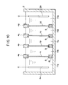
- a plurality of crystalline silicon substrates (1 a-1 d) are arranged in an electrically sealed state at certain intervals through substrate support jigs (4a-4d) as described above along the electric line force of the formation current between the platinum electrodes 3a,3b, whereby the plurality of crystalline silicon substrates can be subjected to the pore-making treatment at the same time.
- the electrolyte has a specific resistance of about 209-cm and serves also as a liquid electrode.
- the formation tank and the substrate support jig except for the crystalline silicon substrate should be made of materials excellent in electric insulating properties.
- a current path is formed through the electrolyte so as to lower the potential difference, whereby the anodization reaction does not proceed near the leakage portion to form a local nonporous region around the leakage portion.
- the conventional sealing member does not have a structure to seal the entire circumference in the peripheral portion on the side surface of the crystalline silicon substrate without a cut or parting, there is a possibility to leak the electrolyte through the junction portion in the substrate support jig in addition to such a problem that labor and time are required for mounting and dismounting the crystalline silicon substrate.
- a problem to be solved is that there is no conventionally available supporting device for substrate, which fully meets the desires to surely prevent the leakage of electrolyte by the treated substrate, to easily mount or dismount the treated substrate, to reduce a production cost, and to simplify the structure.
- a supporting device for treated substrate according to the present invention is applicable to a formation tank in which a chemical treatment is effected on a treated substrate supported in a treating solution, which comprises:
- an integral sealing member without a cut or parting throughout the entire circumference is used for hermetically sealing the peripheral portion of substrate around the entire circumference in close fit to the substrate, so that the treating solution can be surely prevented from leaking.
- the inner diameter of the sealing member is slightly larger than the outer diameter of the treated substrate such as a crystalline silicon substrate; when the pressure is exerted, the inner size of the sealing member becomes perfectly coincident with or slightly smaller than the size of crystalline silicon substrate. Further, a deformation amount of the sealing member and an urging force thereon can be finely adjusted by the air or liquid pressure. Then the treated substrate can be supported without damage while surely preventing the solution from leaking.
- Such a stretchable sealing member is set on the inner circumferential surface of the substrate support jig, which keeps its shape unchanged upon exertion of the pressure, so that the sealing member can be repetitively used as setting, sealing and releasing crystalline silicon substrates one by one.
- Another sealing means in the present invention employs a sealing member of thin tube, which is reversibly or irreversibly heat-shrinkable.
- the tubular sealing member has an inner diameter slightly larger than the outer diameter of crystalline silicon substrate. After the crystalline silicon substrate is inserted inside the tubular sealing member, it is heated to shrink in the normal direction to the crystalline silicon substrate thereby to achieve sealing therebetween.
- the urging force of the sealing member can be finely adjusted by controlling an amount of shrinkage of the tubular sealing member depending upon the heating temperature and the heating time duration.
- a plurality of crystalline silicon substrates having the same shape are set in a tubular sealing member, they are set and heated to shrink one by one in the sealing member as each heated to shrink after set.
- a stretchable sealing member which is similarly tubular but has an inner diameter slightly smaller than the outer diameter of crystalline silicon substrate, the crystalline silicon substrate can be inserted inside the sealing member as expanded, whereby sealing can be achieved in action of shrinking force as a mechanical urging force without relying on heat shrinkage.
- sealing members can seal the entire circumference of crystalline silicon substrate without a cut or junction, they are free of leakage of electrolyte as observed from a junction in a substrate support jig in the conventional sealing member, and the crystalline silicon substrate can be readily mounted to or dismounted from either of the sealing members.
- Fig. 1 is a schematic cross section of an apparatus I in Embodiment 1 of the present invention.
- reference numeral 1 designates a crystalline silicon substrate as a substrate to be treated (treated substrate), 21 a and 21 b electrode support jigs made of a tetrafluoroethylene resin (trade name: Teflon), 3a and 3b platinum electrode plates to which a voltage is applied from an unrepresented external DC power source to constitute negative and positive electrodes, 4 a substrate support jig made of a tetrafluoroethylene resin (trade name: Teflon), constituting substrate supporting means, 5 a substrate sealing member made of a perfluoro elastomer rubber (trade name: Kemraz or Kalrez) similarly having flexibility, elasticity, hermetic property and chemical resistance, 6 a groove, in which the substrate sealing member 5 is set, for uniformly transmitting an air pressure or a liquid pressure onto the sealing member 5, using a space between them, and 7 a pressure supply port for supplying the air
- Numeral 8 denotes outlets for discharging gas generating during formation.
- Numeral 9 denotes formation tank sealing members made of a tetrafluoroethylene resin (trade name: Goatex) having flexibility, elasticity, chemical resistance and hermetic property for preventing an electrolyte from leaking through joint planes between the electrode support jigs 21 a, 21 b and the substrate support jig 4, and 10 bolts for fixing the electrode support jigs 21a, 21 b and the substrate support jig 4 to each other.
- Numerals 11 a and 11 represent the electrolyte, which is a hydrofluoric acid mixture solution.
- Fig. 2A is a cross section to illustrate a positional relation immediately before the crystalline silicon substrate 1 is set in the substrate support jig 4 of the present invention as shown in Fig. 1 or immediately after the setting condition is released. Since Fig. 2A shows a state that the air or liquid pressure is released, the inner diameter of substrate sealing member 5 is larger than the outer diameter of crystalline silicon substrate 1. In this state the crystalline silicon substrate can freely pass inside the substrate sealing member.
- Fig. 2B is a cross section to illustrate a state that the crystalline silicon substrate 1 is set.
- the pressure urges the substrate sealing member 5 along a taper of groove 6 in the normal direction to the crystalline silicon substrate 1 to project it out of the groove 6.
- arrows represent a direction of deformation of the substrate sealing member 5.
- the taper formation in the substrate sealing member 5 and the groove 6 is preferable for hermetically keeping the air or liquid pressure or for preventing a positional deviation of the substrate sealing member 5 relative to the crystalline silicon substrate upon projecting out of the groove.
- the substrate sealing member is made of a perfluoro elastomer rubber (trade name: Kemraz) having an elongation of 200 % at the room temperature.
- the pore-making treatment is carried out as follows on the crystalline silicon substrate.
- a p-type (100) crystalline silicon is produced by the CZ (Czochralski) method as doped with boron (B) to provide a resistivity of 0.01 to 0.02 Qcm.
- B boron
- a wafer is obtained by orientation-flat processing of the thus produced p-type crystalline silicon in diameter 125 mm and thickness 0.6 mm. The wafer is used as the crystalline silicon substrate 1.
- Pressure applying means is compressed air in pressure of 2 kgf/cm 2 from a compressor (not shown) in the pressure supply adjuster 40 in Fig. 1.
- the substrate sealing member 5 has the shape similar to that of the used crystalline silicon substrate 1, but the sealing member 5 has an aperture with inner diameter in a state free of the pressure of compressed air, 2 mm larger than the outer diameter of silicon substrate 1 so that the crystalline silicon substrate 1 may pass freely through the sealing member 5.
- the sealing member 5 has a straight portion corresponding to the orientation flat portion of crystalline silicon substrate 1, and the straight portion has the same length of 42.5 mm as that of substrate.
- an unrepresented vacuum chuck jig When the crystalline silicon substrate 1 is set in the substrate support jig 4, an unrepresented vacuum chuck jig first sucks and supports a flat surface of crystalline silicon substrate 1 in the state that the pressure of compressed air is released, and then locates it in the center of substrate sealing member 5.
- the pressure supply adjuster 40 adjusts the pressure to keep the substrate sealing member 5 in hermetic fit to the entire circumference of crystalline silicon substrate 1. While the pressure is maintained, the vacuum of the vacuum chuck jig is removed.
- the substrate support jig 4 un- itedly supports the crystalline silicon substrate 1 to assure hermetic seal for electrolyte.
- the electrode support jigs 21 a and 21 are connected to the both ends of substrate support jig 4 through the formation tank sealing members 9 and the assembly is secured by the bolts 10.
- Two electrically independent formation cells are formed by the substrate support jig 4, the crystalline silicon substrate 1, and the electrode support jigs 21 a, 21 b.
- a hydrofluoric acid mixture solution in which 48 wt% (% by weight) pure-water-diluted hydrofluoric acid, pure water and alcohol are mixed at a ratio of 1:1:1, is poured into the cells through the outlets 8 to form a body of cathode-side electrolyte 11 a and a body of anode-side electrolyte 11 b.
- the hydrofluoric acid mixture solution has a resistivity of 23.6 Qcm.
- a DC constant-current source (not shown) supplies a current at current density of 8 mA/cm 2 to each of platinum electrodes 3a and 3b.
- the formation reaction starts with the current flow to form pores on the crystalline silicon substrate 1 from the cathode electrode 3a side surface to the anode-side surface.
- Gas such as hydrogen produced in the pore-making treatment is discharged out of the formation cells through the outlets 8.
- the pure water is then discharged and thereafter the bolts 10 are unscrewed to separate the electrode support jigs 21a, 21 b and the substrate support jig 4, disassembling the formation tank.
- the crystalline silicon substrate 1 is then supported by the vacuum chuck (not shown) and the compressed air applied onto the substrate sealing member 5 is released.
- the substrate sealing member 5 having elasticity restores its original shape to free the crystalline silicon substrate 1.
- a reaction for about twelve minutes formed a porous silicon layer in thickness of 10 /1.m.
- the thickness distribution of porous silicon layer was such that the thickness was 10 ⁇ m at the center of substrate and 11 to 12 /1 .m in the peripheral portion of substrate.
- the thus produced porous silicon had a percentage of pores P (Porosity) of 55 %.
- the porous silicon layer was not formed in the leaking portion at all, though the formation reaction occurred at a certain distance from the leaking portion.
- the porous silicon layer was first formed in thickness of 10 /1.m in the region outside a circle with radius 40 mm about the leaking portion.
- the anodization apparatus of the present invention may be so arranged that the electrolyte overflows the formation cells.
- Fig. 11 shows an example of such anodization apparatus.
- reference numerals 1 a, 1 designate formation cells which can keep the liquid surface of electrolyte above the highest portion of treated substrate, 2a, 2b platinum electrodes, 3 a silicon wafer as a treated substrate, 5a, 5b HF aqueous solution as electrolyte, 6 a wafer holder made of Teflon, and 40 an adjuster for supplying a pressure to the wafer holder.
- Numerals 7a, 7b are overflow tanks for receiving the overflowing solution, and 8a, 8b pumps as electrolyte supply means.
- the pumps 8a, 8b circulate the electrolyte in the formation cells.
- the electrolyte in the formation cell 1 a on the treated surface side of treated substrate overflows the upper wall of formation cell 1 a into the overflow tanks 7a, 7b.
- the overflow tanks 7a, 7b formed around the formation cell 1 a are arranged to be connected to each other, and the overflowing solution thereinto is circulated by the pump 8a to the formation cell 1 a.
- bubbles in the electrolyte are discharged from the upper surface of solution and particles are efficiently discharged into the overflow tanks upon overflow to be then removed by a filter 9a set in a pipe in the circulation system.
- the electrolyte is supplied to overflow and then to be cleaned, so that attachment of particles or bubbles may be reduced to the porous surface of treated substrate, enabling more uniform chemical treatment.
- a conductive bulkhead (such as a wafer) for preventing metal contamination may be provided between the treated substrate and the positive metal electrode to avoid direct contact between the electrolyte and the positive metal electrode.
- the metal is prevented from dissolving into the electrolyte, thus preventing metal contamination on the treated substrate.
- the hermetic contact between the treated substrate and the sealing member is achieved by a sealing member arranged oblique to the main surface of treated substrate and urged against the peripheral portion thereof.
- the present invention permits one of electrodes to be set on the back surface of treated substrate.
- the treated substrate (such as wafer) can be effectively transported in the present invention, using a cassette for carrying the treated substrate as shown in Fig. 12.
- a wafer cassette 108 is formed as a plane-plate member, in which an aperture 108a shaped to fit the contour of wafer as the treated substrate is formed in the central portion.
- a step 108b is formed on the lower portion of inner wall in the aperture 108a as a support portion for supporting the peripheral edge of wafer set in the aperture 108a.
- the step 108b is integrally formed throughout the entire circumference of inner wall in the aperture 108a.
- a wafer seal 107 is provided as a sealing member on the upper surface of the step 108b throughout the entire circumference thereof, and a wafer is mounted on this wafer seal 107.
- the treated substrate can be efficiently transported or mounted to the anodization apparatus or to a semiconductor process system.
- Three sets of substrate support jigs 4 as used in Embodiment 1 of the present invention are provided and intervals of the crystalline silicon substrates 1 are arranged to be 50 mm. Then, a plurality of substrates are subjected to anodization treatment at the same time.
- Such formation tank has the same structure as in Embodiment 1 of the present invention except that the substrates are arranged along the formation current between the platinum electrodes.
- the formation conditions are the same as in Embodiment 1 except that the applied voltage is increased in order to allow the same amount of formation current to flow.
- the thickness of the porous silicon layer was from 10 to 11 ⁇ m in the center of the five crystalline silicon substrates after anodization.
- the substrate support jig 4 utilized deformation of the substrate sealing member 5 by compressed air. However, if there is no need to reuse the substrate support jig, the structure can be further simplified.
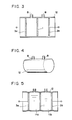
- Fig. 3 is a schematic cross section of an apparatus II in Embodiment 3 of the present invention.
- reference numeral 1 denotes a crystalline silicon substrate, and 3a, 3b platinum electrode plates.
- Numeral 12 denotes a heat-shrinkable tube made of a tetrafluoroethylene resin (Trade name: Teflon) and 8 outlets.
- the outer diameter of the crystalline silicon substrate 1 used is 125 mm as in Embodiment 1.
- the thickness of the heat-shrinkable tube 12 is 0.2 mm. Its cross-sectional shape is shown in Fig. 4 and the tube has an inner diameter 2 mm lager than the outer diameter of the used crystalline silicon substrate and a straight portion with the same length as that of the orientation flat portion, as in Embodiments 1 and 2 of the present invention.
- the shape and the size of the platinum electrode plates 3a, 3b are the same as those of the crystalline silicone substrate 1. Namely, the platinum electrode plates and the crystalline silicon substrate have such sizes that they are movable inside the heat-shrinkable tube 12.
- the platinum electrode plates 3a, 3b and the crystalline silicon substrate 1 are inserted one by one into the heat-shrinkable tube 12 to be set at 50 mm intervals. After the platinum electrode plates and the crystalline silicon substrate are supported by an unrepresented fixing jig through the wall of the heat-shrinkable tube 12, the heat-shrinkable tube 12 is heated to 177 ° C to shrink thereby.
- the heat-shrinkable tube used in the present apparatus II of the invention has a heat shrinkage factor of 77% at the heating temperature, which is full enough to cover the size difference between the tube and the crystalline silicone substrate.
- the heating is continued until the heat-shrinkable tube 12 is hermetically fitted to around the entire circumference of the crystalline silicon substrate 1 and platinum electrode plates 3a, 3b. After completion of the heat shrinkage, the unrepresented fixing jig is removed.
- the whole heat-shrinkable tube may be immersed in a liquid having high electric insulating properties, for example in pure water. This is particularly useful as measure for safety to prevent the platinum electrode plates 3a, 3b from being taken off due to the water pressure of the electrolyte.
- the heat-shrinkable tube is transparent, one can confirm or observe not only the supporting and sealing conditions of the crystalline silicon substrate but also states of the substrate surface and inside the formation cells during anodization.
- the electrolyte is discharged as in the above embodiments.
- the shrinkage of the heat-shrinkable tube utilizes an irreversible deformation with heat. It is thus difficult to utilize the heat deformation again for taking the crystalline silicon substrate and the platinum electrode plates out of the tube. Therefore, the heat-shrinkable tube must be cut to take them out.
- Fig. 6 shows a schematic cross section of an apparatus III in Embodiment 4 of the present invention.
- reference numeral 1 denotes a same crystalline silicon substrate as used in Embodiments 1-3 of the present invention, and 13 an elastic tube made of a perfluoro elastomer rubber (trade name: Kemraz) having an inner diameter slightly smaller than the outer diameter of the crystalline silicon substrate 1.
- the elongation of the tube is 200% and the thickness is 2 mm.
- the cross-sectional shape may be circular.
- the inner diameter of the both end apertures of elastic tube 13 is made larger than the outer diameter of the crystalline silicon substrate in order to facilitate insertion of the crystalline silicon substrate 1 into the tube.
- Numeral 8 denotes outlets.
- Fig. 7 is a schematic cross section to show a state that the platinum electrodes 3a, 3b and the crystalline silicon substrate 1 are set and supported inside the elastic tube 12 in the present apparatus III of the invention.
- the platinum electrodes 3a, 3b and the crystalline silicon substrate 1 are supported one by one by a vacuum chuck (not shown) and then consecutively inserted into the elastic tube 13 as expanded.
- the elastic tube 13 is likely to shrink as to restore its original shape, whereby it hermetically fits to the entire circumferences of the platinum electrodes and the crystalline silicon substrate to thereby support them.
- the electrolyte is poured into the cells through the outlets 8 and a direct current is made to flow through the platinum electrodes to start the anodization reaction.
- the electrolyte After completion of the pore-making treatment on the crystalline silicon substrate 1, the electrolyte is discharged.
- the platinum electrodes 3a, 3b and the crystalline silicon substrate 1 are supported one by one by the vacuum chuck (not shown) and then consecutively pulled out from the end of the elastic tube 13 to the outside.
- the elastic tube 13 restores its original size before the insertion. Thus, it can be used again.
- the apparatus may be immersed in pure water during the anodization in order to cancel the liquid pressure of the electrolyte, as described in the present apparatus II.
- an elastic plate having the same opening can be used in the present invention, though such an embodiment is not shown in a drawing.
- the elastic plate is closely sandwiched and supported between Teflon plates having the same opening.
- the size of the crystalline silicon substrate there is no limitation of the size of the crystalline silicon substrate as long as the size matches the deformation amount of substrate support jig and a substrate support jig for exclusive use is provided.
- the shape of substrate is not limited to disk.
- the shape of the treated substrate is not limited to plate, but the substrate may be spherical or cubic with anodization area limited thereon.
- the apparatus of the present invention can be used for formation reactions other than the pore-making treatment on the crystalline silicon substrate as long as the type and the mixture ratio of electrolyte are properly selected.
- sealing methods in the present invention can be readily used for sealing other liquid or gas materials than the electrolyte of the present invention.
- the present invention can provide a supporting device for substrate having a simple structure, which can certainly prevent the leakage of the treating solution, which is easy in mounting or dismounting the treated substrate and which can be produced in low cost, because the device is so arranged that the treated substrate is hermetically sealed and supported under pressure throughout the entire circumference.
- the anodization apparatus of the invention enjoys an effect of uniform treatment on the treated substrate.
- a supporting device for a treated substrate, applicable to a formation tank in which a chemical treatment is effected on said treated substrate supported in a treating solution comprises:
Abstract
- a sealing member (5) with elasticity for supporting said treated substrate in hermetic fit to a peripheral portion thereof except for a surface to be treated;
- a substrate support jig (4) for supporting said sealing member;
- means (7) for introducing a fluid of gas or liquid from the outside into a hollow portion in said substrate support jig so that a pressure of said fluid urges said sealing member against said peripheral portion except for the surface to be treated on said substrate to achieve hermetic fit therebetween; and
- means for changing said pressure to control a deformation amount of said sealing member and an urging force thereon.
Description
- The present invention relates to a supporting device for substrate which supports a substrate to be treated (hereinafter referred to simply as "treated substrate") in a treating solution, and an anode formation (anodization) apparatus provided with it. More specifically, the present invention relates to an apparatus for anodization of a crystalline silicon layer used in the field of formation technique of Sol (silicon on insulator) which is utilized in ULSI including Bi-CMOS device with both low dissipation power and high-speed operation, three-dimensional structure device including layered functional elements such as a sensor device, an arithmetical element, a memory, etc., or a high- voltage device such as a power transistor for electronic switching system, discharge printer, or plasma display, and in the field of micro machining technique, etc. Particularly, the present invention relates to an anodization apparatus used in producing porous silicon.
- Here, "porous silicon" in the present invention means a crystalline silicon having a single crystal structure and at the same time having many pores therein.
- Further, a term "crystalline silicon substrate" in the present invention means a silicon single crystal wafer having no pores, which is utilized in the field of semiconductor industries.
- Recently, semiconductor devices using porous silicon have been widely researched.
- Formation of porous silicon was found by A. Uhlir and D. R. Turner in the course of study for electrolytic polishing of silicon single crystal which was biased in a positive potential in a hydrofluoric acid (hereinafter referred to simply as "HF") aqueous solution.
- Then, an attempt was made to utilize the high reactivity of porous silicon for an isolation step of elements, which requires a thick insulator formed between elements, in producing a silicon integrated circuit. As a result, application techniques were developed to FIPOS (Full Isolation by Porous Oxidized Silicon), which is a complete isolation technique of IC by a porous silicon oxidized film, and to a silicon direct bonding technique, in which a silicon epitaxial layer grown on a porous silicon substrate is adhered onto an amorphous substrate or onto a silicon single crystal wafer substrate through an oxidized film.
- Inventors of the present invention have been already proposed an anodization apparatus having the structure as shown in a cross section in Fig. 8 as pore-etching apparatus for crystalline silicon utilizing an anodization reaction.
- In Fig. 8,
reference numeral 1 denotes a degenerated crystalline silicon substrate as a substrate to be treated (treated substrate), 2 a formation tank made of a tetrafluoroethylene resin (trade mane: Teflon), 3a and 3b platinum electrode plates to which a voltage is applied from an external direct current (DC) power source (not shown) to constitute negative and positive electrodes, respectively, 4 a substrate support jig made of a tetrafluoroethylene resin (trade name: Teflon) constituting substrate support means, 5 a sealing member for substrate made of a tetrafluoroethylene resin (trade name: Goatex) having flexibility, elasticity and hermetic property, 11 a and 11 b bodies of electrolyte, which is a hydrofluoric acid mixture solution, and 15 a Goatex sealing member for the substrate support jig, which maintains a hermetic contact between theformation tank 2 and thesubstrate support jig 4. - Further, Fig. 9A is a perspective view to illustrate constituent elements in the conventional
substrate support jig 4 shown in Fig. 8, and Fig. 9B a perspective view to show an assembled state of thesupport jig 4. In Figs. 9A and 9B,numerals crystalline silicon substrate 1 can be readily mounted to or dismounted form the jig. -
Numerals support jig segments support jig segments crystalline silicon substrate 1. They are divided in the same manner as the substratesupport jig segments - Crystalline silicon substrates used in semiconductor industries are normally subjected to the orientation flatting processing to indicate the direction of crystallographic axis. Therefore, the segmented substrate sealing member (5a and 5b) and the segmented substrate support jig (4a and 4b) each are shaped asymmetric.
- Numeral 14 denotes bolts made of Teflon, which exert an urging force on the substrate
sealing member segments support jig segments crystalline silicone substrate 1 thereto. By screwing thebolts 14 completely, the entire circumference of thecrystalline silicon substrate 1 and junction planes between the substratesupport jig segments electrolyte bodies - After the
substrate support jig 4 is assembled, the supportjig sealing member 15 made of Goatex is set on a groove in the circumference of thesubstrate support jig 4, and then the assembly is inserted into theformation tank 2, whereby theelectrolyte bodies 11 a, 11 can be separated from each other electrically and hermetically. - Here, the anode-
side electrolyte 11 b serves as a liquid electrode. Further, electrical barrier is made on a surface of thecrystalline silicone substrate 1 facing the cathode-side electrolyte 11 a due to the difference in work function between the electrolyte and the crystalline silicon substrate. Numeral 8 denotes the direction of a formation current. - Then, the external DC power source (not shown) supplies a current to form a cathode of the
platinum electrode 3a and an anode of theplatinum electrode 3b, whereby fluorine ions (hereinafter referred to simply as "F~ ions") are generated in theelectrolyte 11 a in theformation tank 2. The F- ions react with silicon atoms on the cathode-side surface of thesilicon wafer 1 to form tetrafluorosilicon (SiF4) and hydrogen (H2), whereby thesilicon wafer 1 is dissolved while forming pores. - It is known that in formation of pores by the anodization reaction of crystalline silicon, presence of holes in a silicon wafer plays an important role. The mechanism of the formation is considered as follows.
- First, when holes inside a degenerated p-type silicon reach the surface of silicon single crystal wafer, a F- ion starts nucleophilic attack on a Si-H bond compensating for a dangling bond of silicon on the surface, to form a Si-F bond instead thereof.
- Since a F atom has a greater electronegativity than that of a Si atom, polarization induction occurs due to the thus bonded F- ion. Then, another Si-H bond on the surface is attacked by another F- ion to form another Si-F bond, whereby a H2 molecule is produced and at the same time an electron is injected into the anode. By the polarization in the Si-H bond, an electron density in each of back bonds is lowered to make Si-Si bonds weaker.
- These weakened bonds are attacked by HF or H20, so that the Si atom on the crystal surface forms SiF4, which is released from the surface. The crystal surface is terminated by hydrogen or oxygen. A recess formed on the crystal surface by the release of a Si atom generates an electric field distribution which predominantly attracts holes, whereby the surface heterogeneity becomes enhanced thereby to form a pore along the direction of electric field.
- Generally speaking, the above-mentioned electrolyte is usually used in combination with alcohol. The added alcohol prevents hydrogen gas generated during the reaction from adhering to the surface, then interfering supply of hydrofluoric acid to the surface, and in turn impeding the reaction. The above-mentioned predominant formation of pores also occurs in a degenerated n-type silicon in which holes are minority carriers. In this case, the formation of electron-hole pairs upon irradiation with light is a supply source of holes.
- In the conventional anodization apparatus as described above, the
crystalline silicon substrate 1 is arranged to effect electrical seal of the electrolyte throughout the entire circumference in the peripheral portion of the beveled side surface, so that the cathode-side surface of thecrystalline silicon substrate 1 can be uniformly treated to form many pores. - Further, since the cross sectional structure of the apparatus is electrically symmetrical with respect to the
crystalline silicon substrate 1, the both surfaces or entire region of thecrystalline silicon substrate 1 can be subjected to the pore-making treatment by inversion of the polarity of the voltage applied to theplatinum electrodes - Furthermore, in another example as shown in Fig. 10, a plurality of crystalline silicon substrates (1 a-1 d) are arranged in an electrically sealed state at certain intervals through substrate support jigs (4a-4d) as described above along the electric line force of the formation current between the
platinum electrodes - In the conventional anodization apparatus, the electrolyte has a specific resistance of about 209-cm and serves also as a liquid electrode.
- Further, since the anodization reaction proceeds by a potential difference due to the electric barrier between the cathode-side surface and the anode-side surface of the crystalline silicon substrate, it is needless to say that the formation tank and the substrate support jig except for the crystalline silicon substrate should be made of materials excellent in electric insulating properties.
- Accordingly, very careful attention is required in assembling the substrate support jig to prevent the electrolyte from leaking through between the peripheral portion of the crystalline silicon substrate and the sealing member, or through the junction in the substrate support jig.
- Particularly, in the case that the electrolyte leaks in the vicinity of the crystalline silicon substrate, a current path is formed through the electrolyte so as to lower the potential difference, whereby the anodization reaction does not proceed near the leakage portion to form a local nonporous region around the leakage portion.
- Such an unevenness of the thickness of the porous silicon layer formed on the surface of the crystalline silicon substrate cannot be permissible in its applications to products and is a serious problem.
- In addition, from the industrial viewpoint, when a plurality of crystalline silicon substrates are subjected to the pore-making treatment at the same time, it is important to assure certain and easy support of the substrate and leakage prevention of the electrolyte.
- However, since the conventional sealing member does not have a structure to seal the entire circumference in the peripheral portion on the side surface of the crystalline silicon substrate without a cut or parting, there is a possibility to leak the electrolyte through the junction portion in the substrate support jig in addition to such a problem that labor and time are required for mounting and dismounting the crystalline silicon substrate.
- In summary, a problem to be solved is that there is no conventionally available supporting device for substrate, which fully meets the desires to surely prevent the leakage of electrolyte by the treated substrate, to easily mount or dismount the treated substrate, to reduce a production cost, and to simplify the structure.
- It is an object of the present invention to provide a supporting device for substrate having a simple structure, which can surely prevent the leakage of electrolyte by the treated substrate, to which the treated substrate can be easily mounted or dismounted, and which can be produced in a reduced production cost.
- It is another object of the present invention to provide a supporting device for a treated substrate, applicable to a formation tank in which a chemical treatment is effected on a treated substrate supported in a treating solution, comprising:
- a sealing member with elasticity for supporting said treated substrate in hermetic fit to a peripheral portion thereof except for a surface to be treated;
- a substrate support jig for supporting said sealing member;
- means for introducing a fluid of gas or liquid from the outside into a hollow portion in said substrate support jig so that a pressure of said fluid urges said sealing member against said peripheral portion except for the surface to be treated on said substrate to achieve hermetic fit therebetween; and
- means for changing said pressure to control a deformation amount of said sealing member and an urging force thereon.
- It is another object of the present invention to provide an improved anodization apparatus provided with the above-mentioned supporting device.
- It is a further object of the present invention to further improve members used in the supporting device for substrate or in the anodization apparatus.
-
- Fig. 1 is a schematic drawing to show an example of anodization apparatus according to the present invention;
- Figs. 2A and 2B are schematic drawings to illustrate a method for supporting a substrate in the anodization apparatus shown in Fig. 1;
- Fig. 3 is a schematic drawing to show another example of anodization apparatus;
- Fig. 4 is a schematic drawing to show a heat-shrinkable tube used in the apparatus shown in Fig. 3;
- Fig. 5 is a schematic drawing to illustrate a state that a treated substrate and the electrodes are supported in the apparatus shown in Fig. 3;
- Fig. 6 is a schematic drawing to show another example of anodization apparatus;
- Fig. 7 is a schematic drawing to illustrate a state that a treated substrate and the electrodes are supported in the apparatus shown in Fig. 6;
- Fig. 8 is a schematic drawing to show the structure of a conventional anodization apparatus;
- Fig. 9A is a perspective view to show constituent elements in a conventional substrate support jig;
- Fig. 9B is a perspective view to show an assembled state of the conventional substrate support jig shown in Fig. 9A;
- Fig. 10 is a schematic drawing to show a conventional anodization apparatus for treating a plurality of substrates;
- Fig. 11 is a schematic drawing to show another example of anodization apparatus; and
- Fig. 12 is a schematic drawing to show a carrying cassette for treated substrate.
- A supporting device for treated substrate according to the present invention is applicable to a formation tank in which a chemical treatment is effected on a treated substrate supported in a treating solution, which comprises:
- a sealing member with elasticity for supporting said treated substrate in hermetic fit to a peripheral portion thereof except for a surface to be treated;
- a substrate support jig for supporting said sealing member;
- means for introducing a fluid of gas or liquid from the outside into a hollow portion in said substrate support jig so that a pressure of said fluid urges said sealing member against said peripheral portion except for the surface to be treated on said substrate to achieve hermetic fit therebetween; and
- means for changing said pressure to control a deformation amount of said sealing member and the urging force thereon. An anodization apparatus according to the present invention is provided with the supporting device for treated substrate as described above.
- In the present invention, an integral sealing member without a cut or parting throughout the entire circumference is used for hermetically sealing the peripheral portion of substrate around the entire circumference in close fit to the substrate, so that the treating solution can be surely prevented from leaking.
- When the pressure is released, the inner diameter of the sealing member is slightly larger than the outer diameter of the treated substrate such as a crystalline silicon substrate; when the pressure is exerted, the inner size of the sealing member becomes perfectly coincident with or slightly smaller than the size of crystalline silicon substrate. Further, a deformation amount of the sealing member and an urging force thereon can be finely adjusted by the air or liquid pressure. Then the treated substrate can be supported without damage while surely preventing the solution from leaking.
- Such a stretchable sealing member is set on the inner circumferential surface of the substrate support jig, which keeps its shape unchanged upon exertion of the pressure, so that the sealing member can be repetitively used as setting, sealing and releasing crystalline silicon substrates one by one.
- Another sealing means in the present invention employs a sealing member of thin tube, which is reversibly or irreversibly heat-shrinkable.
- The tubular sealing member has an inner diameter slightly larger than the outer diameter of crystalline silicon substrate. After the crystalline silicon substrate is inserted inside the tubular sealing member, it is heated to shrink in the normal direction to the crystalline silicon substrate thereby to achieve sealing therebetween.
- In this case, the urging force of the sealing member can be finely adjusted by controlling an amount of shrinkage of the tubular sealing member depending upon the heating temperature and the heating time duration.
- In case that a plurality of crystalline silicon substrates having the same shape are set in a tubular sealing member, they are set and heated to shrink one by one in the sealing member as each heated to shrink after set.
- Further, employing a stretchable sealing member, which is similarly tubular but has an inner diameter slightly smaller than the outer diameter of crystalline silicon substrate, the crystalline silicon substrate can be inserted inside the sealing member as expanded, whereby sealing can be achieved in action of shrinking force as a mechanical urging force without relying on heat shrinkage.
- Since the sealing members can seal the entire circumference of crystalline silicon substrate without a cut or junction, they are free of leakage of electrolyte as observed from a junction in a substrate support jig in the conventional sealing member, and the crystalline silicon substrate can be readily mounted to or dismounted from either of the sealing members.
- The present invention will be described in more detail with reference to the accompanying drawings.
- Fig. 1 is a schematic cross section of an apparatus I in
Embodiment 1 of the present invention. In Fig. 1,reference numeral 1 designates a crystalline silicon substrate as a substrate to be treated (treated substrate), 21 a and 21 b electrode support jigs made of a tetrafluoroethylene resin (trade name: Teflon), 3a and 3b platinum electrode plates to which a voltage is applied from an unrepresented external DC power source to constitute negative and positive electrodes, 4 a substrate support jig made of a tetrafluoroethylene resin (trade name: Teflon), constituting substrate supporting means, 5 a substrate sealing member made of a perfluoro elastomer rubber (trade name: Kemraz or Kalrez) similarly having flexibility, elasticity, hermetic property and chemical resistance, 6 a groove, in which thesubstrate sealing member 5 is set, for uniformly transmitting an air pressure or a liquid pressure onto the sealingmember 5, using a space between them, and 7 a pressure supply port for supplying the air or liquid pressure from an externalpressure supply system 40 into the space (hollow portion) formed between thegroove 6 and thesubstrate sealing member 5.Numeral 8 denotes outlets for discharging gas generating during formation.Numeral 9 denotes formation tank sealing members made of a tetrafluoroethylene resin (trade name: Goatex) having flexibility, elasticity, chemical resistance and hermetic property for preventing an electrolyte from leaking through joint planes between the electrode support jigs 21 a, 21 b and thesubstrate support jig electrode support jigs substrate support jig 4 to each other.Numerals 11 a and 11 represent the electrolyte, which is a hydrofluoric acid mixture solution. - Fig. 2A is a cross section to illustrate a positional relation immediately before the
crystalline silicon substrate 1 is set in thesubstrate support jig 4 of the present invention as shown in Fig. 1 or immediately after the setting condition is released. Since Fig. 2A shows a state that the air or liquid pressure is released, the inner diameter ofsubstrate sealing member 5 is larger than the outer diameter ofcrystalline silicon substrate 1. In this state the crystalline silicon substrate can freely pass inside the substrate sealing member. - Fig. 2B is a cross section to illustrate a state that the
crystalline silicon substrate 1 is set. In Fig. 2B, when the air or liquid pressure is supplied from thepressure supply port 7, the pressure urges thesubstrate sealing member 5 along a taper ofgroove 6 in the normal direction to thecrystalline silicon substrate 1 to project it out of thegroove 6. In Fig. 2B, arrows represent a direction of deformation of thesubstrate sealing member 5. The taper formation in thesubstrate sealing member 5 and thegroove 6 is preferable for hermetically keeping the air or liquid pressure or for preventing a positional deviation of thesubstrate sealing member 5 relative to the crystalline silicon substrate upon projecting out of the groove. The substrate sealing member is made of a perfluoro elastomer rubber (trade name: Kemraz) having an elongation of 200 % at the room temperature. - In the present apparatus I of the invention the pore-making treatment is carried out as follows on the crystalline silicon substrate. First, a p-type (100) crystalline silicon is produced by the CZ (Czochralski) method as doped with boron (B) to provide a resistivity of 0.01 to 0.02 Qcm. Then a wafer is obtained by orientation-flat processing of the thus produced p-type crystalline silicon in diameter 125 mm and thickness 0.6 mm. The wafer is used as the
crystalline silicon substrate 1. - Pressure applying means is compressed air in pressure of 2 kgf/cm2 from a compressor (not shown) in the
pressure supply adjuster 40 in Fig. 1. Thesubstrate sealing member 5 has the shape similar to that of the usedcrystalline silicon substrate 1, but the sealingmember 5 has an aperture with inner diameter in a state free of the pressure of compressed air, 2 mm larger than the outer diameter ofsilicon substrate 1 so that thecrystalline silicon substrate 1 may pass freely through the sealingmember 5. The sealingmember 5 has a straight portion corresponding to the orientation flat portion ofcrystalline silicon substrate 1, and the straight portion has the same length of 42.5 mm as that of substrate. - When the
crystalline silicon substrate 1 is set in thesubstrate support jig 4, an unrepresented vacuum chuck jig first sucks and supports a flat surface ofcrystalline silicon substrate 1 in the state that the pressure of compressed air is released, and then locates it in the center ofsubstrate sealing member 5. - Then the compressed air is applied to the
substrate sealing member 5 to deform it in the normal direction to the substrate. Thepressure supply adjuster 40 adjusts the pressure to keep thesubstrate sealing member 5 in hermetic fit to the entire circumference ofcrystalline silicon substrate 1. While the pressure is maintained, the vacuum of the vacuum chuck jig is removed. - In this state, the
substrate support jig 4 un- itedly supports thecrystalline silicon substrate 1 to assure hermetic seal for electrolyte. - The electrode support jigs 21 a and 21 are connected to the both ends of
substrate support jig 4 through the formationtank sealing members 9 and the assembly is secured by thebolts 10. - Two electrically independent formation cells are formed by the
substrate support jig 4, thecrystalline silicon substrate 1, and the electrode support jigs 21 a, 21 b. - A hydrofluoric acid mixture solution, in which 48 wt% (% by weight) pure-water-diluted hydrofluoric acid, pure water and alcohol are mixed at a ratio of 1:1:1, is poured into the cells through the
outlets 8 to form a body of cathode-side electrolyte 11 a and a body of anode-side electrolyte 11 b. The hydrofluoric acid mixture solution has a resistivity of 23.6 Qcm. - A DC constant-current source (not shown) supplies a current at current density of 8 mA/cm2 to each of
platinum electrodes - The formation reaction starts with the current flow to form pores on the
crystalline silicon substrate 1 from thecathode electrode 3a side surface to the anode-side surface. Gas such as hydrogen produced in the pore-making treatment is discharged out of the formation cells through theoutlets 8. - After a porous silicon layer is formed in a desired thickness, the direct current is stopped and the electrolyte is discharged through the
outlets 8. Then pure water is poured into the formation cells to wash thecrystalline silicon substrate 1. - The pure water is then discharged and thereafter the
bolts 10 are unscrewed to separate theelectrode support jigs substrate support jig 4, disassembling the formation tank. - The
crystalline silicon substrate 1 is then supported by the vacuum chuck (not shown) and the compressed air applied onto thesubstrate sealing member 5 is released. Thesubstrate sealing member 5 having elasticity restores its original shape to free thecrystalline silicon substrate 1. - According to the above process, a reaction for about twelve minutes formed a porous silicon layer in thickness of 10 /1.m. In a surface of crystalline silicon substrate with diameter 125 mm, the thickness distribution of porous silicon layer was such that the thickness was 10 µm at the center of substrate and 11 to 12 /1.m in the peripheral portion of substrate.
- The thus produced porous silicon had a percentage of pores P (Porosity) of 55 %.
- In a comparative example using the conventional sealing method, if leakage of electrolyte took place due to imperfect seal, the porous silicon layer was not formed in the leaking portion at all, though the formation reaction occurred at a certain distance from the leaking portion. The porous silicon layer was first formed in thickness of 10 /1.m in the region outside a circle with
radius 40 mm about the leaking portion. - The anodization apparatus of the present invention may be so arranged that the electrolyte overflows the formation cells. Fig. 11 shows an example of such anodization apparatus.
- In Fig. 11,
reference numerals - In this apparatus, the
pumps - The electrolyte in the
formation cell 1 a on the treated surface side of treated substrate overflows the upper wall offormation cell 1 a into theoverflow tanks overflow tanks formation cell 1 a are arranged to be connected to each other, and the overflowing solution thereinto is circulated by thepump 8a to theformation cell 1 a. In this occasion, bubbles in the electrolyte are discharged from the upper surface of solution and particles are efficiently discharged into the overflow tanks upon overflow to be then removed by a filter 9a set in a pipe in the circulation system. - In the apparatus shown in Fig. 11, the electrolyte is supplied to overflow and then to be cleaned, so that attachment of particles or bubbles may be reduced to the porous surface of treated substrate, enabling more uniform chemical treatment.
- In the present invention, a conductive bulkhead (such as a wafer) for preventing metal contamination may be provided between the treated substrate and the positive metal electrode to avoid direct contact between the electrolyte and the positive metal electrode. In such an arrangement, the metal is prevented from dissolving into the electrolyte, thus preventing metal contamination on the treated substrate.
- Also, such an arrangement can be employed in the present invention that the hermetic contact between the treated substrate and the sealing member is achieved by a sealing member arranged oblique to the main surface of treated substrate and urged against the peripheral portion thereof.
- Further, the present invention permits one of electrodes to be set on the back surface of treated substrate.
- In addition, the treated substrate (such as wafer) can be effectively transported in the present invention, using a cassette for carrying the treated substrate as shown in Fig. 12.
- In Fig. 12, a
wafer cassette 108 is formed as a plane-plate member, in which anaperture 108a shaped to fit the contour of wafer as the treated substrate is formed in the central portion. Astep 108b is formed on the lower portion of inner wall in theaperture 108a as a support portion for supporting the peripheral edge of wafer set in theaperture 108a. Thestep 108b is integrally formed throughout the entire circumference of inner wall in theaperture 108a. Awafer seal 107 is provided as a sealing member on the upper surface of thestep 108b throughout the entire circumference thereof, and a wafer is mounted on thiswafer seal 107. - In the present invention, using the treated substrate carrying cassette shown in Fig. 12, the treated substrate can be efficiently transported or mounted to the anodization apparatus or to a semiconductor process system.
- Five sets of
substrate support jigs 4 as used inEmbodiment 1 of the present invention are provided and intervals of thecrystalline silicon substrates 1 are arranged to be 50 mm. Then, a plurality of substrates are subjected to anodization treatment at the same time. Such formation tank has the same structure as inEmbodiment 1 of the present invention except that the substrates are arranged along the formation current between the platinum electrodes. - The formation conditions are the same as in
Embodiment 1 except that the applied voltage is increased in order to allow the same amount of formation current to flow. - The thickness of the porous silicon layer was from 10 to 11 µm in the center of the five crystalline silicon substrates after anodization.
- In
Embodiments substrate support jig 4 utilized deformation of thesubstrate sealing member 5 by compressed air. However, if there is no need to reuse the substrate support jig, the structure can be further simplified. - Fig. 3 is a schematic cross section of an apparatus II in
Embodiment 3 of the present invention. - In Fig. 3,
reference numeral 1 denotes a crystalline silicon substrate, and 3a, 3b platinum electrode plates.Numeral 12 denotes a heat-shrinkable tube made of a tetrafluoroethylene resin (Trade name: Teflon) and 8 outlets. - The outer diameter of the
crystalline silicon substrate 1 used is 125 mm as inEmbodiment 1. The thickness of the heat-shrinkable tube 12 is 0.2 mm. Its cross-sectional shape is shown in Fig. 4 and the tube has aninner diameter 2 mm lager than the outer diameter of the used crystalline silicon substrate and a straight portion with the same length as that of the orientation flat portion, as inEmbodiments platinum electrode plates crystalline silicone substrate 1. Namely, the platinum electrode plates and the crystalline silicon substrate have such sizes that they are movable inside the heat-shrinkable tube 12. - The
platinum electrode plates crystalline silicon substrate 1 are inserted one by one into the heat-shrinkable tube 12 to be set at 50 mm intervals. After the platinum electrode plates and the crystalline silicon substrate are supported by an unrepresented fixing jig through the wall of the heat-shrinkable tube 12, the heat-shrinkable tube 12 is heated to 177 ° C to shrink thereby. The heat-shrinkable tube used in the present apparatus II of the invention has a heat shrinkage factor of 77% at the heating temperature, which is full enough to cover the size difference between the tube and the crystalline silicone substrate. - The heating is continued until the heat-
shrinkable tube 12 is hermetically fitted to around the entire circumference of thecrystalline silicon substrate 1 andplatinum electrode plates - By the above operation, two formation cells, which are electrically separated from each other, are formed in the heat-
shrinkable tube 12 in a simple structure. - Then, an electrolyte is poured into the cells through the
outlets 8 and a direct current is made to flow through theplatinum electrode plates - Further, the whole heat-shrinkable tube may be immersed in a liquid having high electric insulating properties, for example in pure water. This is particularly useful as measure for safety to prevent the
platinum electrode plates - However, attention should be paid to prevent the pure water from flowing through the
outlets 8 into the formation cells and thereby to keep the mixture ratio of the electrolyte unchanged. - Since the heat-shrinkable tube is transparent, one can confirm or observe not only the supporting and sealing conditions of the crystalline silicon substrate but also states of the substrate surface and inside the formation cells during anodization.
- After completion of the treatment, the electrolyte is discharged as in the above embodiments.
- Here, the shrinkage of the heat-shrinkable tube utilizes an irreversible deformation with heat. It is thus difficult to utilize the heat deformation again for taking the crystalline silicon substrate and the platinum electrode plates out of the tube. Therefore, the heat-shrinkable tube must be cut to take them out.
- Next described is a method for supporting a substrate using a shrinking force of an elastic tube after expanded, which is opposite to
Embodiment 3. - Fig. 6 shows a schematic cross section of an apparatus III in
Embodiment 4 of the present invention. - In Fig. 6,
reference numeral 1 denotes a same crystalline silicon substrate as used in Embodiments 1-3 of the present invention, and 13 an elastic tube made of a perfluoro elastomer rubber (trade name: Kemraz) having an inner diameter slightly smaller than the outer diameter of thecrystalline silicon substrate 1. The elongation of the tube is 200% and the thickness is 2 mm. - Since the tube can change its shape freely, the cross-sectional shape may be circular.
- The inner diameter of the both end apertures of
elastic tube 13 is made larger than the outer diameter of the crystalline silicon substrate in order to facilitate insertion of thecrystalline silicon substrate 1 into the tube.Numeral 8 denotes outlets. - Further, Fig. 7 is a schematic cross section to show a state that the
platinum electrodes crystalline silicon substrate 1 are set and supported inside theelastic tube 12 in the present apparatus III of the invention. - The
platinum electrodes crystalline silicon substrate 1 are supported one by one by a vacuum chuck (not shown) and then consecutively inserted into theelastic tube 13 as expanded. - In this occasion, the
elastic tube 13 is likely to shrink as to restore its original shape, whereby it hermetically fits to the entire circumferences of the platinum electrodes and the crystalline silicon substrate to thereby support them. - Then, as in the present apparatus II of the invention, the electrolyte is poured into the cells through the
outlets 8 and a direct current is made to flow through the platinum electrodes to start the anodization reaction. - After completion of the pore-making treatment on the
crystalline silicon substrate 1, the electrolyte is discharged. - Next, in the reverse order to the above insertion operation, the
platinum electrodes crystalline silicon substrate 1 are supported one by one by the vacuum chuck (not shown) and then consecutively pulled out from the end of theelastic tube 13 to the outside. - After taking the
crystalline silicon substrate 1 and theplatinum electrodes elastic tube 13 restores its original size before the insertion. Thus, it can be used again. - Also in case of the present apparatus III of the invention, the apparatus may be immersed in pure water during the anodization in order to cancel the liquid pressure of the electrolyte, as described in the present apparatus II.
- Instead of the elastic tube as used in present apparatus III of the invention, an elastic plate having the same opening can be used in the present invention, though such an embodiment is not shown in a drawing. In this case, the elastic plate is closely sandwiched and supported between Teflon plates having the same opening.
- In the above embodiments, there is no limitation of the size of the crystalline silicon substrate as long as the size matches the deformation amount of substrate support jig and a substrate support jig for exclusive use is provided. Thus, the shape of substrate is not limited to disk.
- Further, the shape of the treated substrate is not limited to plate, but the substrate may be spherical or cubic with anodization area limited thereon.
- Furthermore, the apparatus of the present invention can be used for formation reactions other than the pore-making treatment on the crystalline silicon substrate as long as the type and the mixture ratio of electrolyte are properly selected.
- Yet furthermore, a part of the sealing methods in the present invention can be readily used for sealing other liquid or gas materials than the electrolyte of the present invention.
- As detailed above, the present invention can provide a supporting device for substrate having a simple structure, which can certainly prevent the leakage of the treating solution, which is easy in mounting or dismounting the treated substrate and which can be produced in low cost, because the device is so arranged that the treated substrate is hermetically sealed and supported under pressure throughout the entire circumference. Particularly, the anodization apparatus of the invention enjoys an effect of uniform treatment on the treated substrate.
- A supporting device for a treated substrate, applicable to a formation tank in which a chemical treatment is effected on said treated substrate supported in a treating solution comprises:
- a sealing member with elasticity for supporting said treated substrate in hermetic fit to a peripheral portion thereof except for a surface to be treated;
- a substrate support jig for supporting said sealing member;
- means for introducing a fluid of gas or liquid from the outside into a hollow portion in said substrate support jig so that a pressure of said fluid urges said sealing member against said peripheral portion except for the surface to be treated on said substrate to achieve hermetic fit therebetween; and
- means for changing said pressure to control a deformation amount of said sealing member and an urging force thereon.
Claims (7)
Applications Claiming Priority (14)
| Application Number | Priority Date | Filing Date | Title |
|---|---|---|---|
| JP32229592A JP3110178B2 (en) | 1992-11-09 | 1992-11-09 | Method for producing semiconductor substrate and anodizing apparatus |
| JP322295/92 | 1992-11-09 | ||
| JP73293A JP3181128B2 (en) | 1993-01-06 | 1993-01-06 | Semiconductor process equipment |
| JP732/93 | 1993-01-06 | ||
| JP21637/93 | 1993-01-18 | ||
| JP2163793A JPH06216110A (en) | 1993-01-18 | 1993-01-18 | Anode formation method and device |
| JP86876/93 | 1993-03-23 | ||
| JP08687693A JP3416190B2 (en) | 1993-03-23 | 1993-03-23 | Anodizing apparatus and method |
| JP95011/93 | 1993-03-31 | ||
| JP05095011A JP3129569B2 (en) | 1993-03-31 | 1993-03-31 | Anodizing equipment and method |
| JP12207793A JP3201875B2 (en) | 1993-04-27 | 1993-04-27 | Anodizing equipment and method |
| JP122077/93 | 1993-04-27 | ||
| JP135117/93 | 1993-05-14 | ||
| JP13511793A JPH06326084A (en) | 1993-05-14 | 1993-05-14 | Anode formation device |
Publications (2)
| Publication Number | Publication Date |
|---|---|
| EP0597428A1 true EP0597428A1 (en) | 1994-05-18 |
| EP0597428B1 EP0597428B1 (en) | 1997-07-30 |
Family
ID=27563084
Family Applications (1)
| Application Number | Title | Priority Date | Filing Date |
|---|---|---|---|
| EP93118093A Expired - Lifetime EP0597428B1 (en) | 1992-11-09 | 1993-11-08 | Anodization apparatus with supporting device for substrate to be treated |
Country Status (3)
| Country | Link |
|---|---|
| US (1) | US5458755A (en) |
| EP (1) | EP0597428B1 (en) |
| DE (1) | DE69312636T2 (en) |
Cited By (10)
| Publication number | Priority date | Publication date | Assignee | Title |
|---|---|---|---|---|
| EP0846790A2 (en) * | 1996-11-28 | 1998-06-10 | Canon Kabushiki Kaisha | Anodizing apparatus and apparatus and method associated with the same |
| EP0926269A2 (en) * | 1997-12-26 | 1999-06-30 | Canon Kabushiki Kaisha | Anodizing apparatus and method and porous substrate |
| EP2387458A1 (en) * | 2009-01-15 | 2011-11-23 | Solexel, Inc. | Porous silicon electro-etching system and method |
| US9076642B2 (en) | 2009-01-15 | 2015-07-07 | Solexel, Inc. | High-Throughput batch porous silicon manufacturing equipment design and processing methods |
| EP2619790A4 (en) * | 2010-09-24 | 2015-11-11 | Solexel Inc | High-throughput batch porous silicon manufacturing equipment design and processing methods |
| EP2652774A4 (en) * | 2010-11-03 | 2016-04-27 | Solexel Inc | Apparatus and methods for uniformly forming porous semiconductor on a substrate |
| US9401276B2 (en) | 2010-02-12 | 2016-07-26 | Solexel, Inc. | Apparatus for forming porous silicon layers on at least two surfaces of a plurality of silicon templates |
| EP3124655A1 (en) | 2015-07-31 | 2017-02-01 | Silimixt | Adaptable supporting device for substrates to be treated in particular chemically or electrochemically |
| FR3039564A1 (en) * | 2015-07-31 | 2017-02-03 | Silimixt | SUPPORT DEVICE FOR SUBSTRATE TO BE PROCESSED IN PARTICULAR BY CHEMICAL OR ELECTROCHEMICAL |
| CN109056049A (en) * | 2018-08-16 | 2018-12-21 | 湖南文理学院 | A kind of preparation method of nano-structure porous silicon biconcave lens |
Families Citing this family (55)
| Publication number | Priority date | Publication date | Assignee | Title |
|---|---|---|---|---|
| SE500333C2 (en) * | 1993-03-17 | 1994-06-06 | Herman Georg Grimmeiss | Apparatus for electrolytic oxidation of silicon wafers |
| US5824199A (en) * | 1993-11-22 | 1998-10-20 | E. I. Du Pont De Nemours And Company | Electrochemical cell having an inflatable member |
| DE69533245D1 (en) * | 1994-03-25 | 2004-08-19 | Nec Electronics Corp | Electrolytic treatment device |
| JP3985065B2 (en) * | 1997-05-14 | 2007-10-03 | 忠弘 大見 | Porous silicon substrate forming method and porous silicon substrate forming apparatus |
| SG71903A1 (en) | 1998-01-30 | 2000-04-18 | Canon Kk | Process of reclamation of soi substrate and reproduced substrate |
| DE19803852C2 (en) * | 1998-01-31 | 2003-12-18 | Bosch Gmbh Robert | Process for the production of silicon wafers oxidized on both sides |
| JPH11243076A (en) * | 1998-02-26 | 1999-09-07 | Canon Inc | Anodization method and apparatus and manufacture of semiconductor substrate |
| JP3762144B2 (en) | 1998-06-18 | 2006-04-05 | キヤノン株式会社 | Method for manufacturing SOI substrate |
| JP2000082679A (en) | 1998-07-08 | 2000-03-21 | Canon Inc | Semiconductor substrate and production thereof |
| US6197654B1 (en) * | 1998-08-21 | 2001-03-06 | Texas Instruments Incorporated | Lightly positively doped silicon wafer anodization process |
| US6417069B1 (en) | 1999-03-25 | 2002-07-09 | Canon Kabushiki Kaisha | Substrate processing method and manufacturing method, and anodizing apparatus |
| US6410436B2 (en) | 1999-03-26 | 2002-06-25 | Canon Kabushiki Kaisha | Method of cleaning porous body, and process for producing porous body, non-porous film or bonded substrate |
| US6468923B1 (en) | 1999-03-26 | 2002-10-22 | Canon Kabushiki Kaisha | Method of producing semiconductor member |
| DE19914905A1 (en) * | 1999-04-01 | 2000-10-05 | Bosch Gmbh Robert | Electrochemical etching cell for etching silicon wafers uses electrode materials that do not contaminate and/or damage the etching body after etching |
| DE19936569B4 (en) * | 1999-08-03 | 2006-04-27 | Robert Bosch Gmbh | Production of porous silicon |
| TW587332B (en) | 2000-01-07 | 2004-05-11 | Canon Kk | Semiconductor substrate and process for its production |
| JP2002075917A (en) * | 2000-08-25 | 2002-03-15 | Canon Inc | Device and method for separating sample |
| US6454917B1 (en) * | 2000-10-30 | 2002-09-24 | Taiwan Semiconductor Manufacturing Co., Ltd. | High throughput and high performance copper electroplating tool |
| JP3892703B2 (en) * | 2001-10-19 | 2007-03-14 | 富士通株式会社 | Semiconductor substrate jig and semiconductor device manufacturing method using the same |
| US20040124088A1 (en) * | 2002-12-26 | 2004-07-01 | Canon Kabushiki Kaisha | Processing apparatus |
| JP4438049B2 (en) * | 2003-08-11 | 2010-03-24 | キヤノン株式会社 | Field effect transistor, sensor using the same, and manufacturing method thereof |
| US7323731B2 (en) | 2003-12-12 | 2008-01-29 | Canon Kabushiki Kaisha | Photoelectric conversion device, method of manufacturing photoelectric conversion device, and image pickup system |
| JP2005210062A (en) * | 2003-12-26 | 2005-08-04 | Canon Inc | Semiconductor member, manufacturing method therefor, and semiconductor device |
| US9508886B2 (en) | 2007-10-06 | 2016-11-29 | Solexel, Inc. | Method for making a crystalline silicon solar cell substrate utilizing flat top laser beam |
| US8399331B2 (en) | 2007-10-06 | 2013-03-19 | Solexel | Laser processing for high-efficiency thin crystalline silicon solar cell fabrication |
| JP2007297657A (en) * | 2006-04-28 | 2007-11-15 | Canon Inc | Adsorption pat and substrate treatment device |
| JP2008019495A (en) * | 2006-07-14 | 2008-01-31 | Ebara Corp | Method for cleaning porous body, and cleaning device therefor |
| US8035028B2 (en) * | 2006-10-09 | 2011-10-11 | Solexel, Inc. | Pyramidal three-dimensional thin-film solar cells |
| US7999174B2 (en) * | 2006-10-09 | 2011-08-16 | Solexel, Inc. | Solar module structures and assembly methods for three-dimensional thin-film solar cells |
| US20080264477A1 (en) * | 2006-10-09 | 2008-10-30 | Soltaix, Inc. | Methods for manufacturing three-dimensional thin-film solar cells |
| US8084684B2 (en) | 2006-10-09 | 2011-12-27 | Solexel, Inc. | Three-dimensional thin-film solar cells |
| US8193076B2 (en) | 2006-10-09 | 2012-06-05 | Solexel, Inc. | Method for releasing a thin semiconductor substrate from a reusable template |
| WO2009114108A2 (en) | 2008-03-08 | 2009-09-17 | Crystal Solar, Inc. | Integrated method and system for manufacturing monolithic panels of crystalline solar cells |
| EP2356675B1 (en) | 2008-11-13 | 2016-06-01 | Solexel, Inc. | Three dimensional thin film solar cell and manufacturing method thereof |
| US8906218B2 (en) | 2010-05-05 | 2014-12-09 | Solexel, Inc. | Apparatus and methods for uniformly forming porous semiconductor on a substrate |
| US9890465B2 (en) * | 2009-01-15 | 2018-02-13 | Trutag Technologies, Inc. | Apparatus and methods for uniformly forming porous semiconductor on a substrate |
| US9318644B2 (en) | 2009-05-05 | 2016-04-19 | Solexel, Inc. | Ion implantation and annealing for thin film crystalline solar cells |
| MY165969A (en) * | 2009-05-05 | 2018-05-18 | Solexel Inc | High-productivity porous semiconductor manufacturing equipment |
| US20130167915A1 (en) | 2009-12-09 | 2013-07-04 | Solexel, Inc. | High-efficiency photovoltaic back-contact solar cell structures and manufacturing methods using three-dimensional semiconductor absorbers |
| ITMI20100407A1 (en) * | 2010-03-12 | 2011-09-13 | Rise Technology S R L | PHOTO-VOLTAIC CELL WITH REGIONS OF POROUS SEMICONDUCTOR FOR ANCHORING CONTACT TERMINALS |
| JP5489855B2 (en) | 2010-05-14 | 2014-05-14 | キヤノン株式会社 | Method for manufacturing solid-state imaging device |
| WO2011156657A2 (en) | 2010-06-09 | 2011-12-15 | Solexel, Inc. | High productivity thin film deposition method and system |
| JP5715351B2 (en) * | 2010-06-30 | 2015-05-07 | キヤノン株式会社 | Semiconductor device, manufacturing method thereof, and solid-state imaging device |
| MY158500A (en) | 2010-08-05 | 2016-10-14 | Solexel Inc | Backplane reinforcement and interconnects for solar cells |
| US8992746B2 (en) | 2010-12-02 | 2015-03-31 | Dainippon Screen Mfg. Co., Ltd. | Anodizing apparatus |
| US9748414B2 (en) | 2011-05-20 | 2017-08-29 | Arthur R. Zingher | Self-activated front surface bias for a solar cell |
| JP5908266B2 (en) * | 2011-11-30 | 2016-04-26 | 株式会社Screenホールディングス | Anodizing apparatus, anodizing system including the same, and semiconductor wafer |
| JP6189656B2 (en) | 2013-06-14 | 2017-08-30 | Kyb株式会社 | Power supply member and high-speed plating apparatus including the same |
| JP6193005B2 (en) * | 2013-06-14 | 2017-09-06 | Kyb株式会社 | Holding device and high-speed plating apparatus provided with the same |
| FR3020642B1 (en) * | 2014-04-30 | 2021-07-02 | Turbomeca | DEVICE INTENDED FOR IMPLEMENTING AN ANODIZATION TREATMENT |
| CN106906506B (en) * | 2016-12-29 | 2018-12-25 | 平湖瑞星金属工艺有限公司 | A kind of fixture of communication apparatus surface oxidation treatment |
| JP6847691B2 (en) * | 2017-02-08 | 2021-03-24 | 株式会社荏原製作所 | Substrate holder used with plating equipment and plating equipment |
| EP3530776B1 (en) * | 2018-02-26 | 2020-07-08 | Cockerill Maintenance & Ingenierie S.A. | Localised surface treatment installation and method for industrial parts |
| JP2020105590A (en) | 2018-12-27 | 2020-07-09 | キオクシア株式会社 | Substrate processing apparatus and substrate processing method |
| KR20200104691A (en) * | 2019-02-27 | 2020-09-04 | 주식회사 만도 | Anodizing Apparatus |
Citations (3)
| Publication number | Priority date | Publication date | Assignee | Title |
|---|---|---|---|---|
| FR1183754A (en) * | 1956-11-08 | 1959-07-13 | Device for the partial galvanization of cases, in particular watch cases | |
| CH578054A5 (en) * | 1973-09-07 | 1976-07-30 | Oxy Metal Finishing Corp | Jigs for selective electroplating - using inflatable balloons to mask the interior of the workpieces being plated |
| FR2315028A1 (en) * | 1975-06-17 | 1977-01-14 | Quadrimetal Offset | Jig for holding metal lithographic plates during electrotyping - using inflatable tubes to clamp the plates |
Family Cites Families (9)
| Publication number | Priority date | Publication date | Assignee | Title |
|---|---|---|---|---|
| US2737488A (en) * | 1952-11-20 | 1956-03-06 | Western Electric Co | Electroplating apparatus |
| US2801965A (en) * | 1954-05-06 | 1957-08-06 | Western Electric Co | Plating rack |
| CH460975A (en) * | 1967-05-05 | 1968-08-15 | Charmilles Sa Ateliers | Device for supplying current to a workpiece by electrochemical machining |
| DE1931174B2 (en) * | 1969-06-19 | 1975-09-04 | Siemens Ag, 1000 Berlin Und 8000 Muenchen | Device for electrolytic continuous polishing of rod-shaped workpieces made of zircon alloys |
| US3835017A (en) * | 1972-12-22 | 1974-09-10 | Buckbee Mears Co | Reusable shields for selective electrodeposition |
| US4430179A (en) * | 1981-08-03 | 1984-02-07 | Olin Corporation | Portable method for filter press cell assembly |
| US4605483A (en) * | 1984-11-06 | 1986-08-12 | Michaelson Henry W | Electrode for electro-plating non-continuously conductive surfaces |
| FR2615207B1 (en) * | 1987-05-14 | 1991-11-22 | Framatome Sa | TUBULAR ROD FOR TREATING THE INTERIOR SURFACE OF A TUBE |
| US4898653A (en) * | 1988-09-26 | 1990-02-06 | The Dow Chemical Company | Combination electrolysis cell seal member and membrane tentering means |
-
1993
- 1993-11-08 DE DE69312636T patent/DE69312636T2/en not_active Expired - Lifetime
- 1993-11-08 US US08/148,341 patent/US5458755A/en not_active Expired - Lifetime
- 1993-11-08 EP EP93118093A patent/EP0597428B1/en not_active Expired - Lifetime
Patent Citations (3)
| Publication number | Priority date | Publication date | Assignee | Title |
|---|---|---|---|---|
| FR1183754A (en) * | 1956-11-08 | 1959-07-13 | Device for the partial galvanization of cases, in particular watch cases | |
| CH578054A5 (en) * | 1973-09-07 | 1976-07-30 | Oxy Metal Finishing Corp | Jigs for selective electroplating - using inflatable balloons to mask the interior of the workpieces being plated |
| FR2315028A1 (en) * | 1975-06-17 | 1977-01-14 | Quadrimetal Offset | Jig for holding metal lithographic plates during electrotyping - using inflatable tubes to clamp the plates |
Cited By (18)
| Publication number | Priority date | Publication date | Assignee | Title |
|---|---|---|---|---|
| EP0846790A2 (en) * | 1996-11-28 | 1998-06-10 | Canon Kabushiki Kaisha | Anodizing apparatus and apparatus and method associated with the same |
| EP0846790A3 (en) * | 1996-11-28 | 1999-12-29 | Canon Kabushiki Kaisha | Anodizing apparatus and apparatus and method associated with the same |
| US6202655B1 (en) | 1996-11-28 | 2001-03-20 | Canon Kabushiki Kaisha | Anodizing apparatus and apparatus and method associated with the same |
| US6517697B1 (en) | 1996-11-28 | 2003-02-11 | Canon Kabushiki Kaisha | Anodizing method |
| EP0926269A2 (en) * | 1997-12-26 | 1999-06-30 | Canon Kabushiki Kaisha | Anodizing apparatus and method and porous substrate |
| EP0926269A3 (en) * | 1997-12-26 | 2000-05-31 | Canon Kabushiki Kaisha | Anodizing apparatus and method and porous substrate |
| US6258240B1 (en) | 1997-12-26 | 2001-07-10 | Canon Kabushiki Kaisha | Anodizing apparatus and method |
| CN1092720C (en) * | 1997-12-26 | 2002-10-16 | 佳能株式会社 | Anodizing apparatus and method and porous substrate |
| EP2387458A1 (en) * | 2009-01-15 | 2011-11-23 | Solexel, Inc. | Porous silicon electro-etching system and method |
| EP2387458A4 (en) * | 2009-01-15 | 2012-04-11 | Solexel Inc | Porous silicon electro-etching system and method |
| US9076642B2 (en) | 2009-01-15 | 2015-07-07 | Solexel, Inc. | High-Throughput batch porous silicon manufacturing equipment design and processing methods |
| US9401276B2 (en) | 2010-02-12 | 2016-07-26 | Solexel, Inc. | Apparatus for forming porous silicon layers on at least two surfaces of a plurality of silicon templates |
| EP2619790A4 (en) * | 2010-09-24 | 2015-11-11 | Solexel Inc | High-throughput batch porous silicon manufacturing equipment design and processing methods |
| EP2652774A4 (en) * | 2010-11-03 | 2016-04-27 | Solexel Inc | Apparatus and methods for uniformly forming porous semiconductor on a substrate |
| EP3124655A1 (en) | 2015-07-31 | 2017-02-01 | Silimixt | Adaptable supporting device for substrates to be treated in particular chemically or electrochemically |
| FR3039564A1 (en) * | 2015-07-31 | 2017-02-03 | Silimixt | SUPPORT DEVICE FOR SUBSTRATE TO BE PROCESSED IN PARTICULAR BY CHEMICAL OR ELECTROCHEMICAL |
| FR3039563A1 (en) * | 2015-07-31 | 2017-02-03 | Silimixt | ADAPTABLE SUPPORT DEVICE FOR SUBSTRATES TO BE PROCESSED IN PARTICULAR BY CHEMICAL OR ELECTROCHEMICAL |
| CN109056049A (en) * | 2018-08-16 | 2018-12-21 | 湖南文理学院 | A kind of preparation method of nano-structure porous silicon biconcave lens |
Also Published As
| Publication number | Publication date |
|---|---|
| DE69312636D1 (en) | 1997-09-04 |
| US5458755A (en) | 1995-10-17 |
| EP0597428B1 (en) | 1997-07-30 |
| DE69312636T2 (en) | 1998-02-05 |
Similar Documents
| Publication | Publication Date | Title |
|---|---|---|
| US5458755A (en) | Anodization apparatus with supporting device for substrate to be treated | |
| US6214701B1 (en) | Semiconductor substrate and thin film semiconductor device, method of manufacturing the same, and anodizing apparatus | |
| US6448155B1 (en) | Production method of semiconductor base material and production method of solar cell | |
| KR100306839B1 (en) | Treating method and apparatus utilizing chemical reaction | |
| KR100287502B1 (en) | Semiconductor processing system and substrate processing system | |
| US6200878B1 (en) | SOI substrate processing method | |
| US20060070884A1 (en) | Electrochemical processing apparatus and method | |
| EP0940483A2 (en) | Anodizing method and apparatus and semiconductor substrate manufacturing method | |
| US6417069B1 (en) | Substrate processing method and manufacturing method, and anodizing apparatus | |
| JP3110178B2 (en) | Method for producing semiconductor substrate and anodizing apparatus | |
| JP3416190B2 (en) | Anodizing apparatus and method | |
| JP3337705B2 (en) | Anodizing apparatus and method | |
| JP3149060B2 (en) | Anodizing apparatus, anodizing method and method for manufacturing silicon substrate | |
| AU741464B2 (en) | Anodizing apparatus and method and porous substrate | |
| JPH05198556A (en) | Anodizing device | |
| JP3129569B2 (en) | Anodizing equipment and method | |
| US20220251722A1 (en) | Anodization apparatus and anodization method | |
| JP2000277484A (en) | Anodization device, anodization electrode, processing methdo of substrate, and manufacture of substrate | |
| JP2006131969A (en) | Anodic chemical conversion method and apparatus therefor | |
| CN107004630A (en) | System and method for winding porous silicon formation entirely | |
| AU749905B2 (en) | Anodizing apparatus and apparatus and method associated with the same | |
| JP2001316868A (en) | Sheet for cathode, electrolytic plating apparatus and electrolytic plating method | |
| JP2001053049A (en) | Ozone water generator, equipment for cleaning treatment and method for generating ozone water and method of cleaning treatment | |
| JPH06326084A (en) | Anode formation device | |
| JPH11214353A (en) | Anodizing device, board holder, electrode support tool and board, and treatment method thereof |
Legal Events
| Date | Code | Title | Description |
|---|---|---|---|
| PUAI | Public reference made under article 153(3) epc to a published international application that has entered the european phase |
Free format text: ORIGINAL CODE: 0009012 |
|
| AK | Designated contracting states |
Kind code of ref document: A1 Designated state(s): DE FR GB IT NL |
|
| 17P | Request for examination filed |
Effective date: 19941004 |
|
| 17Q | First examination report despatched |
Effective date: 19950118 |
|
| GRAG | Despatch of communication of intention to grant |
Free format text: ORIGINAL CODE: EPIDOS AGRA |
|
| GRAH | Despatch of communication of intention to grant a patent |
Free format text: ORIGINAL CODE: EPIDOS IGRA |
|
| GRAH | Despatch of communication of intention to grant a patent |
Free format text: ORIGINAL CODE: EPIDOS IGRA |
|
| GRAA | (expected) grant |
Free format text: ORIGINAL CODE: 0009210 |
|
| AK | Designated contracting states |
Kind code of ref document: B1 Designated state(s): DE FR GB IT NL |
|
| REF | Corresponds to: |
Ref document number: 69312636 Country of ref document: DE Date of ref document: 19970904 |
|
| ET | Fr: translation filed | ||
| ITF | It: translation for a ep patent filed |
Owner name: SOCIETA' ITALIANA BREVETTI S.P.A. |
|
| PLBE | No opposition filed within time limit |
Free format text: ORIGINAL CODE: 0009261 |
|
| STAA | Information on the status of an ep patent application or granted ep patent |
Free format text: STATUS: NO OPPOSITION FILED WITHIN TIME LIMIT |
|
| 26N | No opposition filed | ||
| REG | Reference to a national code |
Ref country code: GB Ref legal event code: IF02 |
|
| PGFP | Annual fee paid to national office [announced via postgrant information from national office to epo] |
Ref country code: NL Payment date: 20041103 Year of fee payment: 12 |
|
| PGFP | Annual fee paid to national office [announced via postgrant information from national office to epo] |
Ref country code: GB Payment date: 20041104 Year of fee payment: 12 |
|
| PG25 | Lapsed in a contracting state [announced via postgrant information from national office to epo] |
Ref country code: IT Free format text: LAPSE BECAUSE OF NON-PAYMENT OF DUE FEES;WARNING: LAPSES OF ITALIAN PATENTS WITH EFFECTIVE DATE BEFORE 2007 MAY HAVE OCCURRED AT ANY TIME BEFORE 2007. THE CORRECT EFFECTIVE DATE MAY BE DIFFERENT FROM THE ONE RECORDED. Effective date: 20051108 Ref country code: GB Free format text: LAPSE BECAUSE OF NON-PAYMENT OF DUE FEES Effective date: 20051108 |
|
| PG25 | Lapsed in a contracting state [announced via postgrant information from national office to epo] |
Ref country code: NL Free format text: LAPSE BECAUSE OF NON-PAYMENT OF DUE FEES Effective date: 20060601 |
|
| GBPC | Gb: european patent ceased through non-payment of renewal fee |
Effective date: 20051108 |
|
| NLV4 | Nl: lapsed or anulled due to non-payment of the annual fee |
Effective date: 20060601 |
|
| PGFP | Annual fee paid to national office [announced via postgrant information from national office to epo] |
Ref country code: DE Payment date: 20121130 Year of fee payment: 20 |
|
| PGFP | Annual fee paid to national office [announced via postgrant information from national office to epo] |
Ref country code: FR Payment date: 20121214 Year of fee payment: 20 |
|
| REG | Reference to a national code |
Ref country code: DE Ref legal event code: R071 Ref document number: 69312636 Country of ref document: DE |
|
| PG25 | Lapsed in a contracting state [announced via postgrant information from national office to epo] |
Ref country code: DE Free format text: LAPSE BECAUSE OF EXPIRATION OF PROTECTION Effective date: 20131109 |