EP0600380A2 - Method and device for detection and correction of errors in ATM cell headers - Google Patents
Method and device for detection and correction of errors in ATM cell headers Download PDFInfo
- Publication number
- EP0600380A2 EP0600380A2 EP93119020A EP93119020A EP0600380A2 EP 0600380 A2 EP0600380 A2 EP 0600380A2 EP 93119020 A EP93119020 A EP 93119020A EP 93119020 A EP93119020 A EP 93119020A EP 0600380 A2 EP0600380 A2 EP 0600380A2
- Authority
- EP
- European Patent Office
- Prior art keywords
- atm cell
- error
- syndrome word
- bit
- correction
- Prior art date
- Legal status (The legal status is an assumption and is not a legal conclusion. Google has not performed a legal analysis and makes no representation as to the accuracy of the status listed.)
- Granted
Links
Images


Classifications
-
- H—ELECTRICITY
- H04—ELECTRIC COMMUNICATION TECHNIQUE
- H04L—TRANSMISSION OF DIGITAL INFORMATION, e.g. TELEGRAPHIC COMMUNICATION
- H04L1/00—Arrangements for detecting or preventing errors in the information received
- H04L1/004—Arrangements for detecting or preventing errors in the information received by using forward error control
- H04L1/0056—Systems characterized by the type of code used
- H04L1/0057—Block codes
-
- H—ELECTRICITY
- H04—ELECTRIC COMMUNICATION TECHNIQUE
- H04L—TRANSMISSION OF DIGITAL INFORMATION, e.g. TELEGRAPHIC COMMUNICATION
- H04L1/00—Arrangements for detecting or preventing errors in the information received
- H04L1/004—Arrangements for detecting or preventing errors in the information received by using forward error control
- H04L1/0072—Error control for data other than payload data, e.g. control data
-
- H—ELECTRICITY
- H04—ELECTRIC COMMUNICATION TECHNIQUE
- H04L—TRANSMISSION OF DIGITAL INFORMATION, e.g. TELEGRAPHIC COMMUNICATION
- H04L1/00—Arrangements for detecting or preventing errors in the information received
- H04L1/0078—Avoidance of errors by organising the transmitted data in a format specifically designed to deal with errors, e.g. location
- H04L1/0083—Formatting with frames or packets; Protocol or part of protocol for error control
-
- H—ELECTRICITY
- H04—ELECTRIC COMMUNICATION TECHNIQUE
- H04Q—SELECTING
- H04Q11/00—Selecting arrangements for multiplex systems
- H04Q11/04—Selecting arrangements for multiplex systems for time-division multiplexing
- H04Q11/0428—Integrated services digital network, i.e. systems for transmission of different types of digitised signals, e.g. speech, data, telecentral, television signals
- H04Q11/0478—Provisions for broadband connections
-
- H—ELECTRICITY
- H04—ELECTRIC COMMUNICATION TECHNIQUE
- H04L—TRANSMISSION OF DIGITAL INFORMATION, e.g. TELEGRAPHIC COMMUNICATION
- H04L12/00—Data switching networks
- H04L12/54—Store-and-forward switching systems
- H04L12/56—Packet switching systems
- H04L12/5601—Transfer mode dependent, e.g. ATM
- H04L2012/5638—Services, e.g. multimedia, GOS, QOS
- H04L2012/5646—Cell characteristics, e.g. loss, delay, jitter, sequence integrity
- H04L2012/5647—Cell loss
-
- H—ELECTRICITY
- H04—ELECTRIC COMMUNICATION TECHNIQUE
- H04L—TRANSMISSION OF DIGITAL INFORMATION, e.g. TELEGRAPHIC COMMUNICATION
- H04L12/00—Data switching networks
- H04L12/54—Store-and-forward switching systems
- H04L12/56—Packet switching systems
- H04L12/5601—Transfer mode dependent, e.g. ATM
- H04L2012/5638—Services, e.g. multimedia, GOS, QOS
- H04L2012/5646—Cell characteristics, e.g. loss, delay, jitter, sequence integrity
- H04L2012/5652—Cell construction, e.g. including header, packetisation, depacketisation, assembly, reassembly
Definitions
- This invention refers to a method and a device for detection and correction of errors in ATM (Asynchronous Transfer Mode) cell headers, in which a conversion is made from series to parallel of the n bits in the serial data stream, a n-bit parallel data format being obtained which has a clock rate n times lower than that of the original.
- ATM Asynchronous Transfer Mode
- the invention is for application in digital communications systems.
- a fifth byte of redundant information is added to the four initial bytes in the ATM cell header.
- the method consists in applying the coded data vector to a divider circuit based on a Meggit Decoder with serial data input and, simultaneously, to a storage register.
- the divider circuit which includes a shift register, calculates the so-called "syndrome", such that there is a one-on-one correspondence between this syndrome and the error pattern that is assumed to have occurred.
- the combinational logic circuit that is connected to the outputs of the shift register, is designed to have a "1" at its output if, and only if, the syndrome obtained from the divider circuit corresponds to an error pattern with an error in the next bit to leave the storage register.
- the storage register must first contain an initial value for a correct decoding, which for this particular case, is all registers set to "0", corresponding also to the initial value of the shift register in the polynomial generator used by the CCITT Recommendations mentioned earlier.
- This systematic method works at the same rate as the binary data rate and produces, at its output, the syndrome corresponding to the current input.
- the method described here is also characterised in that the ATM cell headers with a n-bit parallel format are delayed until the syndrome word is completed, the error correction process then being carried out in accordance with the syndrome word generated.
- an individual indication for external use can be produced showing that no error has been detected, that more than one error has been detected, or that an error has been corrected.
- the flowchart in figure 1 illustrates the steps in the method used in the invention.
- the information is received as a serial data stream that forms the ATM cells.
- the ATM cell consisting of a serial data stream 1, is changed to a n-bit parallel data format by means of a series to parallel conversion 2.
- a syndrome word 3 is generated from the n-bit parallel data format of the ATM cell header. The relation between the syndrome word generated and the parallel input data is described later for the case of using eight bits but can be generalised for any value of n.
- the word obtained indicates that no error has occurred, that more than one error has occurred, or the position of the erroneous bit to be corrected when only one error has occurred.
- the ATM cell with a n-bit parallel data format is delayed 4 until the syndrome word is available and an error correction 5 can be performed, when required, taking into account the above syndrome word.
- the corrected ATM cell header is obtained 6, when required, in accordance with the syndrome word.
- an individual indication 7 to the exterior can be generated from the result of the detection and correction process carried out.
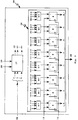
- FIG. 2 shows the device that implements this invention, in which a n-bit parallel data bus 16 is obtained from the ATM cell header with a serial data format 14 by means of a series to parallel converter 9, the parallel data signalling rate being n times lower than the serial data stream 14.
- serial data clock 13 is also divided by n in a frequency divider 8, a parallel data clock 15 being obtained that will be the working frequency for all subsequent digital circuits in the device.
- the device has means 10 to generate a syndrome word 20. They also receive the parallel data clock 15, the n-bit parallel data bus 16, an initialisation signal 17 to set the initial values of the means 10, an ATM cell header indication signal 18 to indicate the ATM cell bits from which the syndrome word 20 has to be calculated, and an indication signal of the last eight bits in the ATM cell header 19, to indicate the inversion 27 of those bits that were previously inverted in the transmission part.
- the syndrome word 20 indicates:
- a delay circuit 11 is shown, the purpose of which is to delay the ATM cell until the syndrome word 20 is available, in this case five cycles of the parallel data clock, and which receives the eight-bit parallel data bus 16 and the parallel data clock 15 to obtain a delayed eight-bit parallel data bus 21.
- the device shown in figure 2 includes error correcting means 12 to correct the ATM cell header according to the previously mentioned table, which receive the delayed eight-bit parallel data bus 21 and the syndrome word 20, and that obtain the corrected ATM cell header, when required, and, optionally, the following three control signals:
Abstract
Description
- This invention refers to a method and a device for detection and correction of errors in ATM (Asynchronous Transfer Mode) cell headers, in which a conversion is made from series to parallel of the n bits in the serial data stream, a n-bit parallel data format being obtained which has a clock rate n times lower than that of the original.
- The invention is for application in digital communications systems.
- In this type of systems it is common to add a few extra bits in the so-called cell header in order to protect the information it contains. In the case of CCITT Recommendations G.707, G.708 and G.709, a fifth byte of redundant information is added to the four initial bytes in the ATM cell header. This fifth byte is termed the protection byte and is produced by means of a cyclic coding with a cyclic code (40, 32) generated by the polynomial

- To extract the error-free initial information, these cyclic codes have to be decoded. One of the decoding methods for cyclic codes is that described in the book "Error Correcting Codes" by W.W. Peterson, published by the Massachusetts Institute of Technology and John Wiley & Sons, Inc, New York and London, 1961, pages 201-204.
- The method consists in applying the coded data vector to a divider circuit based on a Meggit Decoder with serial data input and, simultaneously, to a storage register.
- The divider circuit, which includes a shift register, calculates the so-called "syndrome", such that there is a one-on-one correspondence between this syndrome and the error pattern that is assumed to have occurred. The combinational logic circuit, that is connected to the outputs of the shift register, is designed to have a "1" at its output if, and only if, the syndrome obtained from the divider circuit corresponds to an error pattern with an error in the next bit to leave the storage register.
- The storage register must first contain an initial value for a correct decoding, which for this particular case, is all registers set to "0", corresponding also to the initial value of the shift register in the polynomial generator used by the CCITT Recommendations mentioned earlier.
- The output of the divider circuit can be expressed in matrixial form as:

where - Sts
- is the output of the codes vector from the shift register in the divider circuit, at the time ts,
- Sts+1
- is the output of the codes vector at the time ts+1,
- T
- is a square matrix that represents the codes transformation of the serial divider circuit (transformation matrix), and
- Uts
- is the input vector to the shift register at the time ts.
- This systematic method works at the same rate as the binary data rate and produces, at its output, the syndrome corresponding to the current input.
- The main drawback of this type of method that works in series, in addition to the limitation in the type of integration technology to be used with present-day communications systems which work at increasingly faster speeds, is that the power consumption of devices working in series, whether at current speeds or at speeds foreseen for the near future, can reach levels that are unacceptable in practice.
- Consequently the technical problem to be overcome consists in reducing the total power consumption or, what is the same thing, lowering the working frequency of the digital circuits that perform the error detection and correction function in ATM cell headers.
- To overcome the aforementioned drawbacks, this invention is characterised in that it performs the generation of a syndrome word from the parallel input data in the ATM cell header in accordance with the functional relation:

where - Tn
- is the n-th power of the serial transformation matrix;
- Utp
- is the n-bit input data vector at time tp;
- Stp
- is the syndrome word at time tp; and
- Stp+1
- is the syndrome word at time tp+1;
- . that no error has been detected; or
- . that more than one error has been detected; or
- . the erroneous bit to be corrected when only one error has been detected.
- The method described here is also characterised in that the ATM cell headers with a n-bit parallel format are delayed until the syndrome word is completed, the error correction process then being carried out in accordance with the syndrome word generated.
- Optionally, an individual indication for external use can be produced showing that no error has been detected, that more than one error has been detected, or that an error has been corrected.
- In
claim 4, and in those claims that depend on it, a device is characterised which implements the method of this invention. - With the aforementioned method and device, significant advantages are obtained such as the possibility of using cheaper technologies when the serial data rate is very high (e.g. CMOS instead of ECL), or simply a reduction in power consumption because of the lower working frequency.
- A more detailed explanation of the invention is given in the following description based on the attached figures, in which:
- figure 1 shows a flowchart of the method used in the invention,
- figure 2 shows the block diagram of a device that implements the invention, and
- figure 3 shows a preferred implementation of the means to generate the syndrome word, in accordance with the invention.
- The flowchart in figure 1 illustrates the steps in the method used in the invention. The information is received as a serial data stream that forms the ATM cells.
- The ATM cell, consisting of a
serial data stream 1, is changed to a n-bit parallel data format by means of a series toparallel conversion 2. After this, asyndrome word 3 is generated from the n-bit parallel data format of the ATM cell header. The relation between the syndrome word generated and the parallel input data is described later for the case of using eight bits but can be generalised for any value of n. - When the entire ATM cell header has passed through the syndrome generator, the word obtained indicates that no error has occurred, that more than one error has occurred, or the position of the erroneous bit to be corrected when only one error has occurred. In addition, the ATM cell with a n-bit parallel data format is delayed 4 until the syndrome word is available and an
error correction 5 can be performed, when required, taking into account the above syndrome word. - As a result, the corrected ATM cell header is obtained 6, when required, in accordance with the syndrome word. Also, an
individual indication 7 to the exterior can be generated from the result of the detection and correction process carried out. - The block diagram of figure 2 shows the device that implements this invention, in which a n-bit
parallel data bus 16 is obtained from the ATM cell header with a serial data format 14 by means of a series to parallel converter 9, the parallel data signalling rate being n times lower than the serial data stream 14. - The
serial data clock 13 is also divided by n in a frequency divider 8, aparallel data clock 15 being obtained that will be the working frequency for all subsequent digital circuits in the device. - The device has means 10 to generate a
syndrome word 20. They also receive theparallel data clock 15, the n-bitparallel data bus 16, aninitialisation signal 17 to set the initial values of themeans 10, an ATM cellheader indication signal 18 to indicate the ATM cell bits from which thesyndrome word 20 has to be calculated, and an indication signal of the last eight bits in theATM cell header 19, to indicate theinversion 27 of those bits that were previously inverted in the transmission part. - These means 10 to generate a
syndrome word 20 in the specific case where n = 8, are based on applying the serial data stream 14 mathematically, eight times consecutively, to a divider circuit defined by the polynomial

Mathematically it can be probed that the above operation is equivalent to a divider circuit for eight input bits, where the transformation matrix is given by the following expression:
and the output of this divider circuit can be expressed in matrixial form as:

where - Stp
- is the eight-bit intermediate syndrome word at the time tp of the
parallel data clock 15, - Stp+1
- is the eight-bit intermediate syndrome word in the next time period of the
parallel data clock 15, - Utp
- is the eight-bit input vector to the
means 10 for generating thesyndrome word 20, and - T⁸
- has been presented previously and corresponds with the transformation matrix of the parallel divider circuit that relates the intermediate syndrome words between two consecutives cycles of the parallel data clock, and which can be expressed in logic functions as follows:
- A preferred physical implementation is shown in figure 3, under the
reference 26. - After the input of the five bytes in an ATM cell header to these
means 26, thesyndrome word 20 indicates:

- In addition, in figure 2, a
delay circuit 11 is shown, the purpose of which is to delay the ATM cell until thesyndrome word 20 is available, in this case five cycles of the parallel data clock, and which receives the eight-bitparallel data bus 16 and theparallel data clock 15 to obtain a delayed eight-bitparallel data bus 21. - Finally the device shown in figure 2 includes error correcting means 12 to correct the ATM cell header according to the previously mentioned table, which receive the delayed eight-bit
parallel data bus 21 and thesyndrome word 20, and that obtain the corrected ATM cell header, when required, and, optionally, the following three control signals: - no
error indication signal 22, - corrected
error indication signal 23, and - more than one
error indication signal 24.

where the + symbol indicates a modulo-2 sum.
Claims (8)
- METHOD FOR DETECTION AND CORRECTION OF ERRORS IN ATM CELL HEADERS in which a serial to parallel conversion (2) takes place of n bits in the serial data stream (1), obtaining a n-bit parallel data format with a clock rate that is n times lower than the original, and characterised:- in that it performs the generation of a syndrome word (3) from the parallel input data in the ATM cell header in accordance with the functional relation:

whereTn is the n-th power of the serial transformation matrix;Utp is the n-bit input data vector at time tp;Stp is the syndrome word at time tp; andStp+1 is the syndrome word at time tp+1; and- in that the syndrome word (3) generated indicates, for the header of each ATM cell with n-bit parallel format:. that no error has been detected; or. that more than one error has been detected; or. the erroneous bit to be corrected when only one error has been detected. - METHOD FOR DETECTION AND CORRECTION OF ERRORS IN ATM CELL HEADERS according to claim 1, characterized in that the ATM cell headers with a n-bit parallel format, are delayed (4) until the syndrome word is completed, the error correction process (5) then being carried out in accordance with the syndrome word generated and subsequently to obtain (6) a corrected ATM cell header, when required, in accordance with the syndrome word.
- METHOD FOR DETECTION AND CORRECTION OF ERRORS IN ATM CELL HEADERS according to claim 1, characterized in that an individual indication (7) for external use can be produced showing that no error has been detected, that more than one error has been detected, or that one error has been corrected.
- DEVICE FOR DETECTION AND CORRECTION OF ERRORS IN ATM CELL HEADERS comprising a serial to parallel converter (9), in order to obtain a n-bit parallel data bus (16) starting with the original serial data stream (14), and a frequency divider (8) that divides the serial data clock (13) frequency by n to generate a parallel data clock (16) and characterised in that it includes means (10) to generate a syndrome word (20), that receive the n-bit parallel data bus (16), an initialisation control signal (17) to set the initial values of the means (10) above mentioned, and the parallel data clock (15) to set the clock rate of said means (10).
- DEVICE FOR DETECTION AND CORRECTION OF ERRORS IN ATM CELL HEADERS according to claim 4, characterized in that the means (10) to generate the syndrome word (20) also receive an ATM cell header indication signal (18) in order to indicate the bits from which the syndrome word has to be obtained (20).
- DEVICE FOR DETECTION AND CORRECTION OF ERRORS IN ATM CELL HEADERS according to claim 4, characterized in that it also includes:- a delay circuit (11) that receives the n-bit parallel data bus (16) and the parallel data clock (15), and that generates a n-bit parallel data bus (21) delayed by the time necessary to obtain the syndrome word (20) of the received ATM cell header; and- error correction means (12) that receive the syndrome word (20) and the delayed n-bit parallel data bus (21), and that obtain at their output an ATM cell header (25) in accordance with the indications contained in the generated syndrome word (20), as well as individual indications showing that no error has been detected (22), that more than one error has been detected (24), or that one error has been corrected (23).
- DEVICE FOR DETECTION AND CORRECTION OF ERRORS IN ATM CELL HEADERS according to claim 5, characterized in that the means (10) to generate the syndrome word (20) also receive an indication signal of the last eight bits in the ATM cell header (19) for the inversion of those bits that were previously inverted in the transmission part.
- DEVICE FOR DETECTION AND CORRECTION OF ERRORS IN ATM CELL HEADERS according with claim 5, characterized in that the means (10) to generate the syndrome word (20), when the number of bits is n = 8, satisfy the following logic functions:

 (si)t is the i-th bit of the syndrome word (20) at the time t of the intermediate calculation,(si)t+1 is the i-th bit of the syndrome word (20) in the following period t+1 of the intermediate calculation, andUi is the i-th bit of the n-bit parallel data bus (16) that is applied to the means (10) to generate the syndrome word (20).
Applications Claiming Priority (2)
| Application Number | Priority Date | Filing Date | Title |
|---|---|---|---|
| ES09202433A ES2068105B1 (en) | 1992-11-30 | 1992-11-30 | METHOD AND DEVICE FOR DETECTION AND CORRECTION OF ERRORS IN ATM CELL HEADERS. |
| ES9202433 | 1992-11-30 |
Publications (3)
| Publication Number | Publication Date |
|---|---|
| EP0600380A2 true EP0600380A2 (en) | 1994-06-08 |
| EP0600380A3 EP0600380A3 (en) | 1995-03-29 |
| EP0600380B1 EP0600380B1 (en) | 2004-02-04 |
Family
ID=8278968
Family Applications (1)
| Application Number | Title | Priority Date | Filing Date |
|---|---|---|---|
| EP93119020A Expired - Lifetime EP0600380B1 (en) | 1992-11-30 | 1993-11-25 | Method and device for detection and correction of errors in ATM cell headers |
Country Status (8)
| Country | Link |
|---|---|
| US (1) | US5570377A (en) |
| EP (1) | EP0600380B1 (en) |
| JP (1) | JP3429037B2 (en) |
| AT (1) | ATE259124T1 (en) |
| AU (1) | AU669746B2 (en) |
| CA (1) | CA2110207A1 (en) |
| DE (1) | DE69333411T2 (en) |
| ES (1) | ES2068105B1 (en) |
Cited By (6)
| Publication number | Priority date | Publication date | Assignee | Title |
|---|---|---|---|---|
| GB2313748A (en) * | 1996-05-31 | 1997-12-03 | Northern Telecom Ltd | Error detection/correction for ATM cells/frames |
| US5859857A (en) * | 1995-07-24 | 1999-01-12 | Ascom Tech AG, Gesellschaft Fur Industrielle Forschung + Technologien der Ascom | Method for the integration of additional data in digital data packets |
| EP0938206A2 (en) * | 1998-02-24 | 1999-08-25 | Tektronix, Inc. | Parallel synchronous header correction machine for ATM |
| DE19916631A1 (en) * | 1999-04-13 | 2000-10-26 | Siemens Ag | Recurrent bit sequence detection method for ATM |
| FR2805694A1 (en) * | 2000-02-25 | 2001-08-31 | Sagem | Transmission of signals between two local networks, dividing high rate signal to two lower rate signals and multiplexing |
| US6728921B1 (en) | 1996-05-31 | 2004-04-27 | Nortel Networks Limited | Cell based data transmission method |
Families Citing this family (16)
| Publication number | Priority date | Publication date | Assignee | Title |
|---|---|---|---|---|
| JP3454962B2 (en) * | 1995-03-23 | 2003-10-06 | 株式会社東芝 | Error correction code encoder and decoder |
| FR2735889B1 (en) * | 1995-06-22 | 1997-09-05 | Sgs Thomson Microelectronics | SYNDROME CALCULATION CIRCUIT |
| JPH11196006A (en) * | 1997-12-26 | 1999-07-21 | Nec Corp | Parallel processing syndrome calculation circuit and reed solomon decoding circuit |
| US6606726B1 (en) | 2000-06-13 | 2003-08-12 | Telefonaktiebolaget L M Ericsson (Publ) | Optimization of acceptance of erroneous codewords and throughput |
| US6700827B2 (en) | 2001-02-08 | 2004-03-02 | Integrated Device Technology, Inc. | Cam circuit with error correction |
| US7193876B1 (en) | 2003-07-15 | 2007-03-20 | Kee Park | Content addressable memory (CAM) arrays having memory cells therein with different susceptibilities to soft errors |
| US6987684B1 (en) | 2003-07-15 | 2006-01-17 | Integrated Device Technology, Inc. | Content addressable memory (CAM) devices having multi-block error detection logic and entry selective error correction logic therein |
| US6870749B1 (en) | 2003-07-15 | 2005-03-22 | Integrated Device Technology, Inc. | Content addressable memory (CAM) devices with dual-function check bit cells that support column redundancy and check bit cells with reduced susceptibility to soft errors |
| US7304875B1 (en) | 2003-12-17 | 2007-12-04 | Integrated Device Technology. Inc. | Content addressable memory (CAM) devices that support background BIST and BISR operations and methods of operating same |
| US8462532B1 (en) | 2010-08-31 | 2013-06-11 | Netlogic Microsystems, Inc. | Fast quaternary content addressable memory cell |
| US8582338B1 (en) | 2010-08-31 | 2013-11-12 | Netlogic Microsystems, Inc. | Ternary content addressable memory cell having single transistor pull-down stack |
| US8625320B1 (en) | 2010-08-31 | 2014-01-07 | Netlogic Microsystems, Inc. | Quaternary content addressable memory cell having one transistor pull-down stack |
| US8553441B1 (en) | 2010-08-31 | 2013-10-08 | Netlogic Microsystems, Inc. | Ternary content addressable memory cell having two transistor pull-down stack |
| US8837188B1 (en) | 2011-06-23 | 2014-09-16 | Netlogic Microsystems, Inc. | Content addressable memory row having virtual ground and charge sharing |
| US8773880B2 (en) | 2011-06-23 | 2014-07-08 | Netlogic Microsystems, Inc. | Content addressable memory array having virtual ground nodes |
| JP5982869B2 (en) * | 2012-02-28 | 2016-08-31 | 富士ゼロックス株式会社 | Transmission / reception system and program |
Citations (4)
| Publication number | Priority date | Publication date | Assignee | Title |
|---|---|---|---|---|
| JPH03235441A (en) * | 1990-02-09 | 1991-10-21 | Hitachi Ltd | Cell synchronization circuit |
| EP0472149A1 (en) * | 1990-08-20 | 1992-02-26 | Fujitsu Limited | ATM switch using cell division |
| EP0473188A1 (en) * | 1990-08-31 | 1992-03-04 | Kabushiki Kaisha Toshiba | Method of controlling data transmission in ATM network with cell loss priority level |
| US5230002A (en) * | 1991-01-16 | 1993-07-20 | Nec Corporation | Compact device for monitoring ATM cells |
Family Cites Families (11)
| Publication number | Priority date | Publication date | Assignee | Title |
|---|---|---|---|---|
| US3656107A (en) * | 1970-10-23 | 1972-04-11 | Ibm | Automatic double error detection and correction apparatus |
| GB2075227B (en) * | 1980-04-14 | 1984-09-26 | Victor Company Of Japan | Double error correcting system in digital signal reproducing apparatus |
| US4777635A (en) * | 1986-08-08 | 1988-10-11 | Data Systems Technology Corp. | Reed-Solomon code encoder and syndrome generator circuit |
| JPH0213135A (en) * | 1988-06-30 | 1990-01-17 | Sony Corp | Digital signal transmission equipment |
| JP2816223B2 (en) * | 1990-03-02 | 1998-10-27 | 株式会社日立製作所 | Cell synchronization circuit |
| US5119368A (en) * | 1990-04-10 | 1992-06-02 | At&T Bell Laboratories | High-speed time-division switching system |
| IT1240298B (en) * | 1990-04-13 | 1993-12-07 | Industrie Face Stamdard | ELECTRONIC DEVICE FOR THE PARALLEL CORRECTION OF DATA STRINGS PROTECTED BY ERROR DETECTION BY CYCLE CODE |
| US5285446A (en) * | 1990-11-27 | 1994-02-08 | Nec Corporation | Cell flow control unit and method for asynchronous transfer mode switching networks |
| JP2655547B2 (en) * | 1991-03-13 | 1997-09-24 | 富士通株式会社 | CRC calculation method and HEC synchronizer in ATM switching system |
| JPH04334234A (en) * | 1991-05-10 | 1992-11-20 | Nec Corp | Multiprocessing type atm cell error correcting circuit |
| DE69217931T2 (en) * | 1992-07-14 | 1997-09-25 | Alcatel Bell Nv | Error detection and correction device |
-
1992
- 1992-11-30 ES ES09202433A patent/ES2068105B1/en not_active Expired - Fee Related
-
1993
- 1993-11-12 AU AU50620/93A patent/AU669746B2/en not_active Ceased
- 1993-11-25 EP EP93119020A patent/EP0600380B1/en not_active Expired - Lifetime
- 1993-11-25 AT AT93119020T patent/ATE259124T1/en not_active IP Right Cessation
- 1993-11-25 DE DE1993633411 patent/DE69333411T2/en not_active Expired - Lifetime
- 1993-11-29 CA CA002110207A patent/CA2110207A1/en not_active Abandoned
- 1993-11-29 US US08/158,609 patent/US5570377A/en not_active Expired - Lifetime
- 1993-11-30 JP JP30068393A patent/JP3429037B2/en not_active Expired - Fee Related
Patent Citations (4)
| Publication number | Priority date | Publication date | Assignee | Title |
|---|---|---|---|---|
| JPH03235441A (en) * | 1990-02-09 | 1991-10-21 | Hitachi Ltd | Cell synchronization circuit |
| EP0472149A1 (en) * | 1990-08-20 | 1992-02-26 | Fujitsu Limited | ATM switch using cell division |
| EP0473188A1 (en) * | 1990-08-31 | 1992-03-04 | Kabushiki Kaisha Toshiba | Method of controlling data transmission in ATM network with cell loss priority level |
| US5230002A (en) * | 1991-01-16 | 1993-07-20 | Nec Corporation | Compact device for monitoring ATM cells |
Non-Patent Citations (2)
| Title |
|---|
| PATENT ABSTRACTS OF JAPAN, unexamined applications, E field, vol. 16, no. 18, January 17, 1992 THE PATENT OFFICE JAPANESE GOVERNMENT page 19 E 1155; & JP-A-03 235 441 * |
| Wesley Peterson "Error Correcting Codes", M.I.T. Press & J. Wiley & Sons, Inc., New York and London, 1961 pages 201-204 * Totality * * |
Cited By (11)
| Publication number | Priority date | Publication date | Assignee | Title |
|---|---|---|---|---|
| US5859857A (en) * | 1995-07-24 | 1999-01-12 | Ascom Tech AG, Gesellschaft Fur Industrielle Forschung + Technologien der Ascom | Method for the integration of additional data in digital data packets |
| GB2313748A (en) * | 1996-05-31 | 1997-12-03 | Northern Telecom Ltd | Error detection/correction for ATM cells/frames |
| GB2313748B (en) * | 1996-05-31 | 2000-12-20 | Northern Telecom Ltd | Cell based data transmission method |
| US6230297B1 (en) | 1996-05-31 | 2001-05-08 | Nortel Networks Limited | Cell based data transmission method |
| US6728921B1 (en) | 1996-05-31 | 2004-04-27 | Nortel Networks Limited | Cell based data transmission method |
| EP0938206A2 (en) * | 1998-02-24 | 1999-08-25 | Tektronix, Inc. | Parallel synchronous header correction machine for ATM |
| EP0938206A3 (en) * | 1998-02-24 | 2001-06-13 | Tektronix, Inc. | Parallel synchronous header correction machine for ATM |
| DE19916631A1 (en) * | 1999-04-13 | 2000-10-26 | Siemens Ag | Recurrent bit sequence detection method for ATM |
| DE19916631C2 (en) * | 1999-04-13 | 2001-02-08 | Siemens Ag | Method and device for finding a regularly recurring, predefined bit sequence in a serial data stream |
| FR2805694A1 (en) * | 2000-02-25 | 2001-08-31 | Sagem | Transmission of signals between two local networks, dividing high rate signal to two lower rate signals and multiplexing |
| EP1134936A1 (en) * | 2000-02-25 | 2001-09-19 | Sagem S.A. | Method for transmitting signals between two local networks |
Also Published As
| Publication number | Publication date |
|---|---|
| ATE259124T1 (en) | 2004-02-15 |
| DE69333411D1 (en) | 2004-03-11 |
| US5570377A (en) | 1996-10-29 |
| JP3429037B2 (en) | 2003-07-22 |
| AU5062093A (en) | 1994-06-09 |
| ES2068105B1 (en) | 1995-11-01 |
| EP0600380B1 (en) | 2004-02-04 |
| EP0600380A3 (en) | 1995-03-29 |
| CA2110207A1 (en) | 1994-05-31 |
| AU669746B2 (en) | 1996-06-20 |
| JPH077492A (en) | 1995-01-10 |
| ES2068105A1 (en) | 1995-04-01 |
| DE69333411T2 (en) | 2005-01-13 |
Similar Documents
| Publication | Publication Date | Title |
|---|---|---|
| EP0600380B1 (en) | Method and device for detection and correction of errors in ATM cell headers | |
| US4506372A (en) | Method and apparatus for recognizing in a receiver the start of a telegram signal consisting of a bit impulse sequence | |
| JP2655547B2 (en) | CRC calculation method and HEC synchronizer in ATM switching system | |
| JP3046988B2 (en) | Method and apparatus for detecting frame synchronization of data stream | |
| US5844923A (en) | Fast framing of nude ATM by header error check | |
| CN107154836B (en) | Parallel Cyclic Redundancy Check (CRC) method based on Field Programmable Gate Array (FPGA) | |
| US5805617A (en) | Apparatus for computing error correction syndromes | |
| US6049903A (en) | Digital data error detection and correction system | |
| US4691319A (en) | Method and system for detecting a predetermined number of unidirectional errors | |
| US5935269A (en) | CRC code generation circuit, code error detection circuit and CRC circuit having both functions of the CRC code generation circuit and the code error detection circuit | |
| US4476458A (en) | Dual threshold decoder for convolutional self-orthogonal codes | |
| US4698813A (en) | Arrangement for correcting burst errors in shortened cyclical block codes | |
| US5034742A (en) | Message compression encoder and encoding method for a communication channel | |
| JPH07170200A (en) | Crc synchronizer | |
| US5694405A (en) | Encoder and decoder of an error correcting code | |
| JPH10107647A (en) | Cyclic redundancy check | |
| EP0291961B1 (en) | Method of and device for decoding block-coded messages affected by symbol substitutions, insertions and deletions | |
| US5764876A (en) | Method and device for detecting a cyclic code | |
| US5724034A (en) | Device for establishing cell boundaries in a bit stream and CRC calculation | |
| JP2003078421A (en) | Method and device for detecting first position of code series, and decoding method and device using the sames | |
| EP0240921A2 (en) | BCH code signal correcting system | |
| JPH02248120A (en) | Coder/decoder system for errar connection of digital transmitter | |
| EP0431416A2 (en) | Apparatus and method for accessing a cyclic redundancy error check code generated in parallel | |
| CN1798014B (en) | Method for fixing frame through cyclic redundancy code | |
| JPH09130355A (en) | Error correction encoding method and transmitter-receiver |
Legal Events
| Date | Code | Title | Description |
|---|---|---|---|
| PUAI | Public reference made under article 153(3) epc to a published international application that has entered the european phase |
Free format text: ORIGINAL CODE: 0009012 |
|
| AK | Designated contracting states |
Kind code of ref document: A2 Designated state(s): AT BE CH DE FR GB IT LI NL SE |
|
| PUAL | Search report despatched |
Free format text: ORIGINAL CODE: 0009013 |
|
| AK | Designated contracting states |
Kind code of ref document: A3 Designated state(s): AT BE CH DE FR GB IT LI NL SE |
|
| 17P | Request for examination filed |
Effective date: 19950921 |
|
| 17Q | First examination report despatched |
Effective date: 19990927 |
|
| GRAP | Despatch of communication of intention to grant a patent |
Free format text: ORIGINAL CODE: EPIDOSNIGR1 |
|
| GRAS | Grant fee paid |
Free format text: ORIGINAL CODE: EPIDOSNIGR3 |
|
| GRAA | (expected) grant |
Free format text: ORIGINAL CODE: 0009210 |
|
| RAP1 | Party data changed (applicant data changed or rights of an application transferred) |
Owner name: ALCATEL |
|
| AK | Designated contracting states |
Kind code of ref document: B1 Designated state(s): AT BE CH DE FR GB IT LI NL SE |
|
| PG25 | Lapsed in a contracting state [announced via postgrant information from national office to epo] |
Ref country code: NL Free format text: LAPSE BECAUSE OF FAILURE TO SUBMIT A TRANSLATION OF THE DESCRIPTION OR TO PAY THE FEE WITHIN THE PRESCRIBED TIME-LIMIT Effective date: 20040204 Ref country code: LI Free format text: LAPSE BECAUSE OF FAILURE TO SUBMIT A TRANSLATION OF THE DESCRIPTION OR TO PAY THE FEE WITHIN THE PRESCRIBED TIME-LIMIT Effective date: 20040204 Ref country code: CH Free format text: LAPSE BECAUSE OF FAILURE TO SUBMIT A TRANSLATION OF THE DESCRIPTION OR TO PAY THE FEE WITHIN THE PRESCRIBED TIME-LIMIT Effective date: 20040204 Ref country code: BE Free format text: LAPSE BECAUSE OF FAILURE TO SUBMIT A TRANSLATION OF THE DESCRIPTION OR TO PAY THE FEE WITHIN THE PRESCRIBED TIME-LIMIT Effective date: 20040204 Ref country code: AT Free format text: LAPSE BECAUSE OF FAILURE TO SUBMIT A TRANSLATION OF THE DESCRIPTION OR TO PAY THE FEE WITHIN THE PRESCRIBED TIME-LIMIT Effective date: 20040204 |
|
| REG | Reference to a national code |
Ref country code: GB Ref legal event code: FG4D |
|
| REG | Reference to a national code |
Ref country code: CH Ref legal event code: EP |
|
| REF | Corresponds to: |
Ref document number: 69333411 Country of ref document: DE Date of ref document: 20040311 Kind code of ref document: P |
|
| PG25 | Lapsed in a contracting state [announced via postgrant information from national office to epo] |
Ref country code: SE Free format text: LAPSE BECAUSE OF FAILURE TO SUBMIT A TRANSLATION OF THE DESCRIPTION OR TO PAY THE FEE WITHIN THE PRESCRIBED TIME-LIMIT Effective date: 20040504 |
|
| NLV1 | Nl: lapsed or annulled due to failure to fulfill the requirements of art. 29p and 29m of the patents act | ||
| REG | Reference to a national code |
Ref country code: CH Ref legal event code: PL |
|
| ET | Fr: translation filed | ||
| PLBE | No opposition filed within time limit |
Free format text: ORIGINAL CODE: 0009261 |
|
| STAA | Information on the status of an ep patent application or granted ep patent |
Free format text: STATUS: NO OPPOSITION FILED WITHIN TIME LIMIT |
|
| 26N | No opposition filed |
Effective date: 20041105 |
|
| PGFP | Annual fee paid to national office [announced via postgrant information from national office to epo] |
Ref country code: DE Payment date: 20061124 Year of fee payment: 14 Ref country code: FR Payment date: 20061124 Year of fee payment: 14 |
|
| PGFP | Annual fee paid to national office [announced via postgrant information from national office to epo] |
Ref country code: GB Payment date: 20061127 Year of fee payment: 14 |
|
| PGFP | Annual fee paid to national office [announced via postgrant information from national office to epo] |
Ref country code: IT Payment date: 20061130 Year of fee payment: 14 |
|
| REG | Reference to a national code |
Ref country code: FR Ref legal event code: CD |
|
| GBPC | Gb: european patent ceased through non-payment of renewal fee |
Effective date: 20071125 |
|
| PG25 | Lapsed in a contracting state [announced via postgrant information from national office to epo] |
Ref country code: DE Free format text: LAPSE BECAUSE OF NON-PAYMENT OF DUE FEES Effective date: 20080603 |
|
| REG | Reference to a national code |
Ref country code: FR Ref legal event code: ST Effective date: 20080930 |
|
| PG25 | Lapsed in a contracting state [announced via postgrant information from national office to epo] |
Ref country code: GB Free format text: LAPSE BECAUSE OF NON-PAYMENT OF DUE FEES Effective date: 20071125 |
|
| PG25 | Lapsed in a contracting state [announced via postgrant information from national office to epo] |
Ref country code: FR Free format text: LAPSE BECAUSE OF NON-PAYMENT OF DUE FEES Effective date: 20071130 |
|
| PG25 | Lapsed in a contracting state [announced via postgrant information from national office to epo] |
Ref country code: IT Free format text: LAPSE BECAUSE OF NON-PAYMENT OF DUE FEES Effective date: 20071125 |