EP0601075B1 - Electrophoretic display with single character erasure - Google Patents
Electrophoretic display with single character erasure Download PDFInfo
- Publication number
- EP0601075B1 EP0601075B1 EP92919087A EP92919087A EP0601075B1 EP 0601075 B1 EP0601075 B1 EP 0601075B1 EP 92919087 A EP92919087 A EP 92919087A EP 92919087 A EP92919087 A EP 92919087A EP 0601075 B1 EP0601075 B1 EP 0601075B1
- Authority
- EP
- European Patent Office
- Prior art keywords
- display
- conductor members
- matrix
- further characterised
- members
- Prior art date
- Legal status (The legal status is an assumption and is not a legal conclusion. Google has not performed a legal analysis and makes no representation as to the accuracy of the status listed.)
- Expired - Lifetime
Links
Images

Classifications
-
- G—PHYSICS
- G09—EDUCATION; CRYPTOGRAPHY; DISPLAY; ADVERTISING; SEALS
- G09G—ARRANGEMENTS OR CIRCUITS FOR CONTROL OF INDICATING DEVICES USING STATIC MEANS TO PRESENT VARIABLE INFORMATION
- G09G3/00—Control arrangements or circuits, of interest only in connection with visual indicators other than cathode-ray tubes
- G09G3/20—Control arrangements or circuits, of interest only in connection with visual indicators other than cathode-ray tubes for presentation of an assembly of a number of characters, e.g. a page, by composing the assembly by combination of individual elements arranged in a matrix no fixed position being assigned to or needed to be assigned to the individual characters or partial characters
- G09G3/34—Control arrangements or circuits, of interest only in connection with visual indicators other than cathode-ray tubes for presentation of an assembly of a number of characters, e.g. a page, by composing the assembly by combination of individual elements arranged in a matrix no fixed position being assigned to or needed to be assigned to the individual characters or partial characters by control of light from an independent source
- G09G3/3433—Control arrangements or circuits, of interest only in connection with visual indicators other than cathode-ray tubes for presentation of an assembly of a number of characters, e.g. a page, by composing the assembly by combination of individual elements arranged in a matrix no fixed position being assigned to or needed to be assigned to the individual characters or partial characters by control of light from an independent source using light modulating elements actuated by an electric field and being other than liquid crystal devices and electrochromic devices
- G09G3/344—Control arrangements or circuits, of interest only in connection with visual indicators other than cathode-ray tubes for presentation of an assembly of a number of characters, e.g. a page, by composing the assembly by combination of individual elements arranged in a matrix no fixed position being assigned to or needed to be assigned to the individual characters or partial characters by control of light from an independent source using light modulating elements actuated by an electric field and being other than liquid crystal devices and electrochromic devices based on particles moving in a fluid or in a gas, e.g. electrophoretic devices
- G09G3/3446—Control arrangements or circuits, of interest only in connection with visual indicators other than cathode-ray tubes for presentation of an assembly of a number of characters, e.g. a page, by composing the assembly by combination of individual elements arranged in a matrix no fixed position being assigned to or needed to be assigned to the individual characters or partial characters by control of light from an independent source using light modulating elements actuated by an electric field and being other than liquid crystal devices and electrochromic devices based on particles moving in a fluid or in a gas, e.g. electrophoretic devices with more than two electrodes controlling the modulating element
-
- G—PHYSICS
- G02—OPTICS
- G02F—OPTICAL DEVICES OR ARRANGEMENTS FOR THE CONTROL OF LIGHT BY MODIFICATION OF THE OPTICAL PROPERTIES OF THE MEDIA OF THE ELEMENTS INVOLVED THEREIN; NON-LINEAR OPTICS; FREQUENCY-CHANGING OF LIGHT; OPTICAL LOGIC ELEMENTS; OPTICAL ANALOGUE/DIGITAL CONVERTERS
- G02F1/00—Devices or arrangements for the control of the intensity, colour, phase, polarisation or direction of light arriving from an independent light source, e.g. switching, gating or modulating; Non-linear optics
- G02F1/01—Devices or arrangements for the control of the intensity, colour, phase, polarisation or direction of light arriving from an independent light source, e.g. switching, gating or modulating; Non-linear optics for the control of the intensity, phase, polarisation or colour
- G02F1/165—Devices or arrangements for the control of the intensity, colour, phase, polarisation or direction of light arriving from an independent light source, e.g. switching, gating or modulating; Non-linear optics for the control of the intensity, phase, polarisation or colour based on translational movement of particles in a fluid under the influence of an applied field
- G02F1/166—Devices or arrangements for the control of the intensity, colour, phase, polarisation or direction of light arriving from an independent light source, e.g. switching, gating or modulating; Non-linear optics for the control of the intensity, phase, polarisation or colour based on translational movement of particles in a fluid under the influence of an applied field characterised by the electro-optical or magneto-optical effect
- G02F1/167—Devices or arrangements for the control of the intensity, colour, phase, polarisation or direction of light arriving from an independent light source, e.g. switching, gating or modulating; Non-linear optics for the control of the intensity, phase, polarisation or colour based on translational movement of particles in a fluid under the influence of an applied field characterised by the electro-optical or magneto-optical effect by electrophoresis
-
- G—PHYSICS
- G02—OPTICS
- G02F—OPTICAL DEVICES OR ARRANGEMENTS FOR THE CONTROL OF LIGHT BY MODIFICATION OF THE OPTICAL PROPERTIES OF THE MEDIA OF THE ELEMENTS INVOLVED THEREIN; NON-LINEAR OPTICS; FREQUENCY-CHANGING OF LIGHT; OPTICAL LOGIC ELEMENTS; OPTICAL ANALOGUE/DIGITAL CONVERTERS
- G02F1/00—Devices or arrangements for the control of the intensity, colour, phase, polarisation or direction of light arriving from an independent light source, e.g. switching, gating or modulating; Non-linear optics
- G02F1/01—Devices or arrangements for the control of the intensity, colour, phase, polarisation or direction of light arriving from an independent light source, e.g. switching, gating or modulating; Non-linear optics for the control of the intensity, phase, polarisation or colour
- G02F1/165—Devices or arrangements for the control of the intensity, colour, phase, polarisation or direction of light arriving from an independent light source, e.g. switching, gating or modulating; Non-linear optics for the control of the intensity, phase, polarisation or colour based on translational movement of particles in a fluid under the influence of an applied field
- G02F1/1675—Constructional details
- G02F1/16756—Insulating layers
-
- G—PHYSICS
- G09—EDUCATION; CRYPTOGRAPHY; DISPLAY; ADVERTISING; SEALS
- G09G—ARRANGEMENTS OR CIRCUITS FOR CONTROL OF INDICATING DEVICES USING STATIC MEANS TO PRESENT VARIABLE INFORMATION
- G09G2300/00—Aspects of the constitution of display devices
- G09G2300/04—Structural and physical details of display devices
- G09G2300/0421—Structural details of the set of electrodes
- G09G2300/0426—Layout of electrodes and connections
-
- G—PHYSICS
- G09—EDUCATION; CRYPTOGRAPHY; DISPLAY; ADVERTISING; SEALS
- G09G—ARRANGEMENTS OR CIRCUITS FOR CONTROL OF INDICATING DEVICES USING STATIC MEANS TO PRESENT VARIABLE INFORMATION
- G09G2300/00—Aspects of the constitution of display devices
- G09G2300/06—Passive matrix structure, i.e. with direct application of both column and row voltages to the light emitting or modulating elements, other than LCD or OLED
-
- G—PHYSICS
- G09—EDUCATION; CRYPTOGRAPHY; DISPLAY; ADVERTISING; SEALS
- G09G—ARRANGEMENTS OR CIRCUITS FOR CONTROL OF INDICATING DEVICES USING STATIC MEANS TO PRESENT VARIABLE INFORMATION
- G09G2310/00—Command of the display device
- G09G2310/06—Details of flat display driving waveforms
- G09G2310/061—Details of flat display driving waveforms for resetting or blanking
-
- G—PHYSICS
- G09—EDUCATION; CRYPTOGRAPHY; DISPLAY; ADVERTISING; SEALS
- G09G—ARRANGEMENTS OR CIRCUITS FOR CONTROL OF INDICATING DEVICES USING STATIC MEANS TO PRESENT VARIABLE INFORMATION
- G09G2320/00—Control of display operating conditions
- G09G2320/02—Improving the quality of display appearance
- G09G2320/0209—Crosstalk reduction, i.e. to reduce direct or indirect influences of signals directed to a certain pixel of the displayed image on other pixels of said image, inclusive of influences affecting pixels in different frames or fields or sub-images which constitute a same image, e.g. left and right images of a stereoscopic display
Definitions
- Electrophoretic displays are now well known. A variety of display types and features are taught in several patents issued in the names of the inventors herein, Frank J. DiSanto and Denis A. Krusos and assigned to the assignee herein, Copytele, Inc. of Huntington Station New York.
- U.S. Patent Nos. 4,655,897 and 4,732,830 each entitled ELECTROPHORETIC DISPLAY PANELS AND ASSOCIATED METHODS describe the basic operation and construction of an electrophoretic display.
- U.S. Patent No. 4,742,345, entitled ELECTROPHORETIC DISPLAY PANELS AND METHODS THEREFOR describes a display having improved alignment and contrast.
- the display panels shown in the above-mentioned patents operate upon the same basic principle, viz., if a suspension of electrically charged pigment particles in a dielectric fluid is subjected to an applied electrostatic field, the pigment particles will migrate through the fluid in response to the electrostatic field. Given a substantially homogeneous suspension of particles having a pigment color different from that of the dielectric fluid, if the applied electrostatic field is localized it will cause a visually observable localized pigment particle migration. The localized pigment particle migration results either in a localized area of concentration or rarefaction of particles depending upon the sign and direction of the electrostatic field and the charge on the pigment particles.
- Patents are "triode-type" displays having a plurality of independent, parallel, cathode row conductor members deposited in the horizontal on one surface of a glass viewing screen.
- a glass cap member forms a fluid-tight seal with the viewing window along the cap's peripheral edge for containing the fluid suspension and also acts as a substrate for an anode plate deposited on the interior flat surface of the cap.
- the anode surface is in spaced parallel relation to both the cathode members and the grid members.
- the cathode member voltage, the anode voltage, and the grid member voltage can then be ascertained such that when a particular voltage is applied to the cathode and another voltage is applied to the grid, the area proximate their intersection will assume a net charge sufficient to attract or repel pigment particles in suspension in the dielectric fluid. Since numerous cathode and grid lines are employed, there are numerous discrete intersection points which can be controlled by varying the voltage on the cathode and grid members to cause localized visible regions of pigment concentration and rarefaction.
- the operating voltages on both cathode and grid must be able to assume at least two states corresponding to a logical one and a logical zero.
- Logical one for the cathode may either correspond to attraction or repulsion of pigment.
- the cathode and grid voltages are selected such that only when both are a logical one at a particular intersection point, will a sufficient electrostatic field be present at the intersection relative to the anode to cause the writing of a visual bit of information on the display through migration of a pigment particle.
- the bit may be erased, e.g., upon a reversal of polarity and a logical zero-zero state occurring at the intersection coordinated with an erase voltage gradient between anode and cathode. In this manner, digitized data can be displayed on the electrophoretic display.
- an electrophoretic display must be able to assume a blank or erased state; must be able to display character data written during a Write operation; and must be able to continually maintain or hold the written characters (and blank characters) in a Hold mode until they are erased or overwritten.
- These three modes of operation i.e., Erase, Write and Hold are well documented in existing patents issued to the inventors herein. Certain aspects of these modes of operation are repeated herein, however, for the convenience of the reader. See U.S.
- Patent 4,947,157 "APPARATUS AND METHODS FOR PULSING THE ELECTRODES OF AN ELECTROPHORETIC DISPLAY FOR ACHIEVING FASTER DISPLAY OPERATION" issued on August 7, 1990 to Frank DiSanto et al. and assigned to Copytele, Inc.
- the anode face can be completely darkened and the cathode face simultaneously completely lightened by applying a sufficiently large negative voltage on the anode.
- This condition causes the light-colored, negatively charged particles to migrate from the anode to the cathode.
- the negative particles will pass through the grid which would be maintained at a voltage permitting passage of the particles therethrough, for example, at zero voltage.
- such cells or electrophoretic displays essentially contain an anode, a cathode and a grid electrode, which grid electrode further controls the transportation of charged particles.
- the charged particles are transferred and forced against one electrode, as the anode or cathode under the influence of an applied electric field, so that the viewer may view the color of the pigment which forms a desired display pattern.
- the grid electrode is employed to enable control of the migration of such particles. It is also indicated that when the polarity of the field is reversed, the pigment particles are transported and packed on the opposite electrode. This is indicative, for example, of an erasing mode.
- the normal voltages on a typical electrophoretic panel enable the following conditions of operation.
- the panel can be operated in an Erase Mode where the anode electrode is negative with respect to the cathode electrode which is positive. In this mode the grid electrodes are at a low potential which is equivalent for example to a binary O.
- a Hold Mode the anode is positive, the cathodes are positive and the grid electrodes are essentially at zero voltage or at binary 0 level. As one can understand, the cathode operates between zero and positive voltages while the grid operates between low (“0") and high voltages ("1").
- a low condition will be indicated by a binary 0 and a high condition is indicated by a binary 1.
- the anode is positive, the cathodes that are being written into are at zero potential and the grids, which are the writing grids, are at a positive or high potential as a binary 1.
- all non-writing cathodes are positive and non-writing grids are at low potential or more negative than the cathode.
- U.S. Patent No. 5,223,823 relates to another structure for an electrophoretic display in which the previously described grid of electrically independently controllable elements is replaced with a monolithic or electrically continuous grid with pores therein. Further, the monolithic anode is replaced with a plurality of discrete, electrically independent elements.
- pixel writing and erasure is accomplished by impressing a voltage gradient between a selected anode element and a selected intersecting cathode element such that at their point of intersection, the gradient is sufficient to overcome a constant barrier voltage on the monolithic grid element and cause migration of pigment particles past the grid.
- European Application published under No. 0 396 247 relates to an electrophoretic display having a plurality of independent cathode and grid elements.
- a monolithic anode plate remote anode
- a plurality of discrete local anode elements are formed atop and in parallel to either the grid or cathode elements with a corresponding plurality of insulator strips positioned therebetween.
- This structure is achieved, inter alia, by employing different metals for grid and local anode and performing a two-step etching to form these elements.
- Selective erasure at the pixel level may be performed by establishing a sufficient voltage gradient at an intersection point of a selected cathode and grid member relative to the remote anode and lowering the potential of the local anode element crossing the particular intersection to ground potential thereby permitting particle passage.
- U.S. Patent No. 5,066,946 relates to an electrophoretic display of a type having a plurality of independent cathode and grid elements.
- the anode is however, divided into a plurality of discrete elements.
- a selected line rather than the entire display screen, can be erased during an erase operation.
- the independent anode elements are separately addressable and therefore the erase voltage can be impressed upon any selected anode element to erase a line of characters from the display screen.
- the typical screen has about 25 horizontal lines for character text; the individual anode elements are approximately 25 in number; and there is one anode element aligned with a corresponding horizontal line of text.
- All the pixels of an entire line may therefore be erased by impressing the erase voltage upon the corresponding anode element.
- This feature is beneficial in that the entire screen need not be erased and rewritten when sequential screens differ only slightly. If only the display data which has changed is erased and rewritten, screen rewrite time is saved and display energy requirements are reduced.
- EP 0 186 519 A further form of electrophoretic device is described in EP 0 186 519.
- it comprises a plurality of independent cathode and grid elements and an anode divided into a plurality of discrete elements.
- Information is written onto the display either repeatedly for set periods of time or for a single selected period of time, in order to implement a grey scale of brightness. Alternatively, the information may be written once for a short period of time, which gives only partial brightness, but may be adequate in some circumstances.
- an electrophoretic display including a fluid-tight envelope having a portion thereof which is at least partially transparent, an electrophoretic fluid contained within said envelope, said fluid having pigmented particles suspended therein, said electrophoretic display being characterised in that: means for selectively erasing at least one displayed character with an electrostatic charge without erasing other displayed characters, the erasing means including a first addressable X-Y matrix for selectively establishing a discrete electrostatic charge across at least one intersection of the first X-Y matrix, for erasing said at least one displayed character on said display, the erasing means further including a second addressable X-Y matrix for selectively establishing a discrete electrostatic charge across intersections of the second X-Y matrix for writing pixel data on the display.
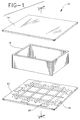
- FIG. 1 is an exploded perspective view of an electrophoretic display in accordance with an exemplary embodiment of the present invention.
- FIG. 3 is an enlarged perspective view of an anode element of the device depicted in FIGS. 1 and 2.
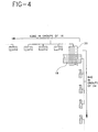
- FIG. 4 is a diagram of a portion of the anode of the display shown in FIGS. 1 and 2 showing an exemplary grouping of anode elements.
- FIG. 1 shows an electrophoretic display 10 in accordance with the present invention.
- the display 10 has an anode faceplate 12 and a cathode faceplate 14 which are sealably affixed on either side of an interstitial wall 16 to form a fluid tight envelope for containing dielectric/pigment particle suspension or electrophoretic fluid (not shown).
- the faceplates 12 and 14 are typically flat glass plates upon which are deposited conductor elements for controlling the electrostatic charge for inducing motion in the electrophoretic fluid.
- the techniques, materials and dimensions used to form conductor elements upon the cathode faceplate, i.e., the cathode and grid, are shown in U.S. Patent Nos. 4,655,897, 4,732,830 and 4,742,345.
- the conductor members on the anode faceplate 12 are configured very similarly to those of the known cathode faceplate 14.
- the horizontal anode elements 18 are produced by etching an Indium-Tin-Oxide (ITO) coated glass plate.
- ITO Indium-Tin-Oxide
- the present invention differs from previous constructs, however, in that a layer of Silicon Dioxide SiO 2 is then deposited over the etched ITO glass surface. Following deposition of the SiO 2 , the conventional construct is continued, i.e., a layer of insulator is then deposited over the SiO 2 layer and the insulator is coated with a metal. The metal is then etched to produce the vertical anode elements 20.
- an x-y matrix of electrically chargeable lines can, via appropriate circuit drivers connected to the lines, be "addressed", such that at any given intersection in the matrix can be impressed with a desired voltage.
- This construct has been employed in the cathode-grid matrix described in the above referenced patents issued to the inventors herein.
- the horizontal and vertical members are grouped, however, as shall be described below.
- U.S. Patent Nos. 4,742,345 and 4,772,820 may be referred to for more verisimilar illustrations of electrophoretic display elements.
- the anode faceplate 12 and the elements 18 and 20, with the exception of the SiO 2 layer, have the same basic form as known cathode/grid faceplates.
- the horizontal anode elements 18 are etched on ITO coated glass as are the conventional horizontal cathode members.
- the vertical anode elements 20 are superimposed on the horizontal members and are insulated therefrom by an interstitial photoresist layer as the grid members are insulated from the cathode members.
- the vertical anode elements are formed by coating the photoresist layer with a metal, such as nickel, using sputtering techniques, or the like, and then masked and etched like the conventional grid elements.
- FIG. 2 shows the electrophoretic display of FIG. 1 assembled in a cross-section.
- the SiO 2 layer 22 deposited over the horizontal anode elements 18 and the supporting anode faceplate 12 surface is visible in this view.
- the remnants of the etched anode insulation layer, i.e., the anode insulator strips 24 can be seen in FIG. 2.
- An examination of the upper portion of FIG. 2 reveals the cathode elements 26, grid elements 28 and grid insulator strips 30 as are known in the art. All conductor elements are quite thin and extend beneath the interstitial wall 16 at at least one end thereof to provide a terminal exterior to the envelope for connecting display driver circuitry (not shown).
- FIG. 3 illustrates the preferred form of the vertical anode elements.
- the elements are slotted or tined.
- 640 horizontal elements be deposited upon the anode screen having an overall width of 112 micrometers, a length approximating the viewing screen width and separated one from the next in the vertical direction by a space of 15 micrometers.
- Groups of 24 horizontal elements are electrically connected at the ends thus giving approximately 26 horizontal anode element groups corresponding to 25 lines of character text to be displayed and erased an additional border area.
- 1280 vertical anode elements be deposited upon the anode screen (atop the SiO 2 layer 22 and anode insulator strips 24), each having a slotted configuration as shown in FIG.
- FIG. 4 diagrammatically depicts the grouping of horizontal 18 and vertical 20 anode elements.
- the anode matrix may be used in conjunction with the cathode and grid to selectively erase single characters at the intersection of particular horizontal 18 and vertical 20 anode element groups, or may be operated as a monolithic anode.
- all horizontal (outer) anode elements 18 may be set positive relative to the cathode, grid and vertical (inner) anode elements 20.
- a selected horizontal element 18 group is made negative relative to intersecting vertical anode elements.
- writing to a selected character location may be enabled or disabled.
Abstract
Description
- The present invention relates to electrophoretic displays, and more particularly to a display capable of selective erasure of displayed data.
- Electrophoretic displays are now well known. A variety of display types and features are taught in several patents issued in the names of the inventors herein, Frank J. DiSanto and Denis A. Krusos and assigned to the assignee herein, Copytele, Inc. of Huntington Station New York. For example, U.S. Patent Nos. 4,655,897 and 4,732,830, each entitled ELECTROPHORETIC DISPLAY PANELS AND ASSOCIATED METHODS describe the basic operation and construction of an electrophoretic display. U.S. Patent No. 4,742,345, entitled ELECTROPHORETIC DISPLAY PANELS AND METHODS THEREFOR, describes a display having improved alignment and contrast. The inventors herein also have several applications relating to electrophoretic displays presently pending in the Patent Office. Three such applications which may have some relevance to the present invention are Application No. 07/375,056 (published as U.S. Patent No. 5,066,946) entitled ELECTROPHORETIC DISPLAY PANEL WITH SELECTIVE LINE ERASURE, Application No. 07/667,630 (published as U.S. Patent No. 5,223,823) entitled ELECTROPHORETIC DISPLAY PANEL WITH PLURAL ELECTRICALLY INDEPENDENT ANODE ELEMENTS and Application No. 07/345,825 (published as a European Patent Application under No. EP 0396247) entitled DUAL ANODE FLAT PANEL ELECTROPHORETIC DISPLAY APPARATUS, each of which shall be described below to point out their potential relevance.
- The display panels shown in the above-mentioned patents operate upon the same basic principle, viz., if a suspension of electrically charged pigment particles in a dielectric fluid is subjected to an applied electrostatic field, the pigment particles will migrate through the fluid in response to the electrostatic field. Given a substantially homogeneous suspension of particles having a pigment color different from that of the dielectric fluid, if the applied electrostatic field is localized it will cause a visually observable localized pigment particle migration. The localized pigment particle migration results either in a localized area of concentration or rarefaction of particles depending upon the sign and direction of the electrostatic field and the charge on the pigment particles. The electrophoretic display apparatus taught in the foregoing U.S. Patents are "triode-type" displays having a plurality of independent, parallel, cathode row conductor members deposited in the horizontal on one surface of a glass viewing screen. A layer of insulating photoresist material deposited over the cathode members and photoetched down to the cathode members to yield a plurality of insulator strips positioned at right angles to the cathode members, forms the substrate for a plurality of independent, parallel column grid conductor members running in the vertical direction. A glass cap member forms a fluid-tight seal with the viewing window along the cap's peripheral edge for containing the fluid suspension and also acts as a substrate for an anode plate deposited on the interior flat surface of the cap. When the cap is in place, the anode surface is in spaced parallel relation to both the cathode members and the grid members. Given a specific particulate suspension, the sign of the electrostatic charge which will attract and repel the pigment particles will be known. The cathode member voltage, the anode voltage, and the grid member voltage can then be ascertained such that when a particular voltage is applied to the cathode and another voltage is applied to the grid, the area proximate their intersection will assume a net charge sufficient to attract or repel pigment particles in suspension in the dielectric fluid. Since numerous cathode and grid lines are employed, there are numerous discrete intersection points which can be controlled by varying the voltage on the cathode and grid members to cause localized visible regions of pigment concentration and rarefaction. Essentially then, the operating voltages on both cathode and grid must be able to assume at least two states corresponding to a logical one and a logical zero. Logical one for the cathode may either correspond to attraction or repulsion of pigment. Typically, the cathode and grid voltages are selected such that only when both are a logical one at a particular intersection point, will a sufficient electrostatic field be present at the intersection relative to the anode to cause the writing of a visual bit of information on the display through migration of a pigment particle. The bit may be erased, e.g., upon a reversal of polarity and a logical zero-zero state occurring at the intersection coordinated with an erase voltage gradient between anode and cathode. In this manner, digitized data can be displayed on the electrophoretic display.
- To be useful as a display, an electrophoretic display must be able to assume a blank or erased state; must be able to display character data written during a Write operation; and must be able to continually maintain or hold the written characters (and blank characters) in a Hold mode until they are erased or overwritten. These three modes of operation, i.e., Erase, Write and Hold are well documented in existing patents issued to the inventors herein. Certain aspects of these modes of operation are repeated herein, however, for the convenience of the reader. See U.S. Patent 4,947,157 "APPARATUS AND METHODS FOR PULSING THE ELECTRODES OF AN ELECTROPHORETIC DISPLAY FOR ACHIEVING FASTER DISPLAY OPERATION" issued on August 7, 1990 to Frank DiSanto et al. and assigned to Copytele, Inc.
- Given a multi-element cathode and multi-element grid structure as described above, a planar anode, electrically negative, light-colored pigment particles, and a dark-colored, electrically-neutral suspension, the anode face can be completely darkened and the cathode face simultaneously completely lightened by applying a sufficiently large negative voltage on the anode. This condition causes the light-colored, negatively charged particles to migrate from the anode to the cathode. On the way to the cathode, the negative particles will pass through the grid which would be maintained at a voltage permitting passage of the particles therethrough, for example, at zero voltage. Once the anode and cathode screens are rendered monochromic by virtue of the accumulation of negatively-charged, light-colored pigment particles on the cathode elements and the absence of pigment particles on the anode, the respective screens may be deemed "erased".
- In any event, if reference is made to the above-noted patents, one will see that such cells or electrophoretic displays essentially contain an anode, a cathode and a grid electrode, which grid electrode further controls the transportation of charged particles. In operation, the charged particles are transferred and forced against one electrode, as the anode or cathode under the influence of an applied electric field, so that the viewer may view the color of the pigment which forms a desired display pattern. In this manner the grid electrode is employed to enable control of the migration of such particles. It is also indicated that when the polarity of the field is reversed, the pigment particles are transported and packed on the opposite electrode. This is indicative, for example, of an erasing mode.
- The normal voltages on a typical electrophoretic panel enable the following conditions of operation. The panel can be operated in an Erase Mode where the anode electrode is negative with respect to the cathode electrode which is positive. In this mode the grid electrodes are at a low potential which is equivalent for example to a binary O. In a Hold Mode the anode is positive, the cathodes are positive and the grid electrodes are essentially at zero voltage or at binary 0 level. As one can understand, the cathode operates between zero and positive voltages while the grid operates between low ("0") and high voltages ("1").
- As indicated above, a low condition will be indicated by a binary 0 and a high condition is indicated by a binary 1. In any event, during a Write Mode the anode is positive, the cathodes that are being written into are at zero potential and the grids, which are the writing grids, are at a positive or high potential as a binary 1. During this mode all non-writing cathodes are positive and non-writing grids are at low potential or more negative than the cathode.
- U.S. Patent No. 5,223,823 relates to another structure for an electrophoretic display in which the previously described grid of electrically independently controllable elements is replaced with a monolithic or electrically continuous grid with pores therein. Further, the monolithic anode is replaced with a plurality of discrete, electrically independent elements. In displays constructed in accordance with the teachings of the aforesaid application, pixel writing and erasure is accomplished by impressing a voltage gradient between a selected anode element and a selected intersecting cathode element such that at their point of intersection, the gradient is sufficient to overcome a constant barrier voltage on the monolithic grid element and cause migration of pigment particles past the grid.
- European Application, published under No. 0 396 247 relates to an electrophoretic display having a plurality of independent cathode and grid elements. In addition to a monolithic anode plate (remote anode), a plurality of discrete local anode elements are formed atop and in parallel to either the grid or cathode elements with a corresponding plurality of insulator strips positioned therebetween. This structure is achieved, inter alia, by employing different metals for grid and local anode and performing a two-step etching to form these elements. Selective erasure at the pixel level may be performed by establishing a sufficient voltage gradient at an intersection point of a selected cathode and grid member relative to the remote anode and lowering the potential of the local anode element crossing the particular intersection to ground potential thereby permitting particle passage.
- U.S. Patent No. 5,066,946 relates to an electrophoretic display of a type having a plurality of independent cathode and grid elements. The anode is however, divided into a plurality of discrete elements. In Patent No. 5,066,946, a selected line, rather than the entire display screen, can be erased during an erase operation. The independent anode elements are separately addressable and therefore the erase voltage can be impressed upon any selected anode element to erase a line of characters from the display screen. In accordance with the foregoing principles, the typical screen has about 25 horizontal lines for character text; the individual anode elements are approximately 25 in number; and there is one anode element aligned with a corresponding horizontal line of text. All the pixels of an entire line may therefore be erased by impressing the erase voltage upon the corresponding anode element. This feature is beneficial in that the entire screen need not be erased and rewritten when sequential screens differ only slightly. If only the display data which has changed is erased and rewritten, screen rewrite time is saved and display energy requirements are reduced.
- A further form of electrophoretic device is described in EP 0 186 519. As for the previous prior art example it comprises a plurality of independent cathode and grid elements and an anode divided into a plurality of discrete elements. Information is written onto the display either repeatedly for set periods of time or for a single selected period of time, in order to implement a grey scale of brightness. Alternatively, the information may be written once for a short period of time, which gives only partial brightness, but may be adequate in some circumstances.
- Whereas the above-described applications teach multi-element anodes for use with a monolithic grid; dual anodes, one being monolithic and the other discrete elements parallel to the grid elements for erasure of single pixels, and, in one instance, single line erasure of an electrophoretic display by means of a multi-element anode, there is no prior teaching concerning a display having a cathode and grid structure like that shown, e.g. in U.S. Patent No. 4,742,345 and having the capacity to selectively erase a single character.
- It is therefore an object of the present invention to provide such an electrophoretic display.
- The problems and disadvantages associated with the selected erasure of conventional electrophoretic displays are overcome by the present invention which includes an electrophoretic display including a fluid-tight envelope having a portion thereof which is at least partially transparent, an electrophoretic fluid contained within said envelope, said fluid having pigmented particles suspended therein, said electrophoretic display being characterised in that:
means for selectively erasing at least one displayed character with an electrostatic charge without erasing other displayed characters, the erasing means including a first addressable X-Y matrix for selectively establishing a discrete electrostatic charge across at least one intersection of the first X-Y matrix, for erasing said at least one displayed character on said display, the erasing means further including a second addressable X-Y matrix for selectively establishing a discrete electrostatic charge across intersections of the second X-Y matrix for writing pixel data on the display. - For a better understanding of the present invention, reference is made to the following detailed description of an exemplary embodiment considered in conjunction with the accompanying drawings, in which:
- FIG. 1 is an exploded perspective view of an electrophoretic display in accordance with an exemplary embodiment of the present invention.
- FIG.2 is a cross-sectional view of the electrophoretic display shown in FIG. 1 in the unexploded state, taken along section line II-II and looking in the direction of the arrows.
- FIG. 3 is an enlarged perspective view of an anode element of the device depicted in FIGS. 1 and 2.
- FIG. 4 is a diagram of a portion of the anode of the display shown in FIGS. 1 and 2 showing an exemplary grouping of anode elements.
- FIG. 1 shows an
electrophoretic display 10 in accordance with the present invention. Thedisplay 10 has ananode faceplate 12 and acathode faceplate 14 which are sealably affixed on either side of aninterstitial wall 16 to form a fluid tight envelope for containing dielectric/pigment particle suspension or electrophoretic fluid (not shown). Thefaceplates - In the present invention, the conductor members on the
anode faceplate 12 are configured very similarly to those of the knowncathode faceplate 14. In particular, thehorizontal anode elements 18 are produced by etching an Indium-Tin-Oxide (ITO) coated glass plate. The present invention differs from previous constructs, however, in that a layer of Silicon Dioxide SiO2 is then deposited over the etched ITO glass surface. Following deposition of the SiO2, the conventional construct is continued, i.e., a layer of insulator is then deposited over the SiO2 layer and the insulator is coated with a metal. The metal is then etched to produce thevertical anode elements 20. Only a few horizontal 18 and vertical 20 anode members are depicted for ease of illustration. Similarly, the shape and proportions of the elements depicted are for purposes of illustration only. In actual displays there are many more elements, e.g., 640 horizontal members and 1280 vertical members. It is common in the art to refer to conductor members like 18 and 20 as "lines". Conductor members oriented in a first direction, such as thehorizontal members 18, are frequently described as extending in the "x-direction". Thevertical members 20 could then be said to run in the "y-direction", so that when viewed along a line approximately perpendicular to the planes containing the "x" and "y" lines, the x and y lines form a cartesian coordinate system or an x-y matrix. As is known in the art, an x-y matrix of electrically chargeable lines can, via appropriate circuit drivers connected to the lines, be "addressed", such that at any given intersection in the matrix can be impressed with a desired voltage. This construct has been employed in the cathode-grid matrix described in the above referenced patents issued to the inventors herein. The horizontal and vertical members are grouped, however, as shall be described below. U.S. Patent Nos. 4,742,345 and 4,772,820 may be referred to for more verisimilar illustrations of electrophoretic display elements. - Essentially then, the
anode faceplate 12 and theelements horizontal anode elements 18 are etched on ITO coated glass as are the conventional horizontal cathode members. Thevertical anode elements 20 are superimposed on the horizontal members and are insulated therefrom by an interstitial photoresist layer as the grid members are insulated from the cathode members. The vertical anode elements are formed by coating the photoresist layer with a metal, such as nickel, using sputtering techniques, or the like, and then masked and etched like the conventional grid elements. Thus, the anode is a matrix of a plurality of elongated, parallel,horizontal members 18 upon which is superimposed a plurality of elongated parallelvertical members 20, a strip of insulator electrically and physically separating the two sets of anode elements. - FIG. 2 shows the electrophoretic display of FIG. 1 assembled in a cross-section. The SiO2 layer 22 deposited over the
horizontal anode elements 18 and the supportinganode faceplate 12 surface is visible in this view. Similarly, the remnants of the etched anode insulation layer, i.e., the anode insulator strips 24 can be seen in FIG. 2. An examination of the upper portion of FIG. 2 reveals thecathode elements 26,grid elements 28 and grid insulator strips 30 as are known in the art. All conductor elements are quite thin and extend beneath theinterstitial wall 16 at at least one end thereof to provide a terminal exterior to the envelope for connecting display driver circuitry (not shown). - FIG. 3 illustrates the preferred form of the vertical anode elements. As can be seen, the elements are slotted or tined. It is preferred that 640 horizontal elements be deposited upon the anode screen having an overall width of 112 micrometers, a length approximating the viewing screen width and separated one from the next in the vertical direction by a space of 15 micrometers. Groups of 24 horizontal elements are electrically connected at the ends thus giving approximately 26 horizontal anode element groups corresponding to 25 lines of character text to be displayed and erased an additional border area. It is preferred that 1280 vertical anode elements be deposited upon the anode screen (atop the SiO2 layer 22 and anode insulator strips 24), each having a slotted configuration as shown in FIG. 3 and an overall width of 112 micrometers, a length approximating the viewing screen height and separated one from the next in the horizontal direction by a space of 15 micrometers. Groups of 16 vertical elements (not just the tines) are connected at the ends thus giving 80 vertical anode element groups corresponding to the 80 columns of character text to be displayed and erased. It is preferred that the slots in the vertical anode elements be extended through the insulation layer (strips) 24 as is taught in U.S. Patent No. 4,742,345.
- FIG. 4 diagrammatically depicts the grouping of horizontal 18 and vertical 20 anode elements.
- In operation, the anode matrix may be used in conjunction with the cathode and grid to selectively erase single characters at the intersection of particular horizontal 18 and vertical 20 anode element groups, or may be operated as a monolithic anode. For example, in single character erase mode, all horizontal (outer)
anode elements 18 may be set positive relative to the cathode, grid and vertical (inner)anode elements 20. When a desired character is to be erased, a selectedhorizontal element 18 group is made negative relative to intersecting vertical anode elements. Thus, at the intersection, and only at the intersection, is the barrier caused by thevertical element 20 group lowered and a sufficient voltage gradient established to induce pigment particle migration. In a similar manner, writing to a selected character location may be enabled or disabled.
Claims (22)
- An electrophoretic display (10) including a fluid-tight envelope (12,14,16) having a portion thereof which is at least partially transparent, an electrophoretic fluid contained within said envelope (12,14,16), said fluid having pigmented particles suspended therein, said electrophoretic display (10) being characterised in that:
means for selectively erasing at least one displayed character with an electrostatic charge without erasing other displayed characters, the erasing means including a first addressable X-Y matrix (18,20) for selectively establishing a discrete electrostatic charge across at least one intersection of the first X-Y matrix (18,20), for erasing said at least one displayed character on said display, the erasing means further including a second addressable X-Y matrix (26,28) for selectively establishing a discrete electrostatic charge across intersections of the second X-Y matrix (26,28) for writing pixel data on the display (10). - The display (10) of Claim 1, further characterised in that the first addressable X-Y matrix having a first plurality of conductor members in the X-direction (18) and a first plurality of conductor members in the Y-direction (20).
- The display (10) of Claim 2, further characterised in that the second addressable X-Y matrix having a second plurality of conductor members in the X-direction (26) and a second plurality of conductor members in the Y-direction (28).
- The display (10) of Claim 3, further characterised in that the first and second matrices are substantially parallel and the intersections thereof occupy fixed positions relative to each other.
- The display (10) of Claim 4, further characterised in that the intersections of the first matrix (18,20) and the intersections of the second matrix (26,28) exhibit a fixed relative alignment such that each intersection of the second matrix (26,28) is spatially associated with a corresponding intersection of the first matrix (18,20).
- The display (10) of Claim 5, further characterised in that the X and Y conductor members of the first and second matrices assume voltage levels such that at the respective intersections thereof display data may be written and erased under the control of an electrostatic field established between the corresponding intersections.
- The display (10) of Claim 6, further characterised in that each of the intersections of the second matrix (26,28) serves as the loci for a displayable pixel and the intersections of the first matrix (18,20) have an area at least as small as the area of a displayable character composed of displayable pixels.
- The display (10) of Claim 3, further characterised in that the envelope includes a first flat faceplate (12), a central portion of which is the transparent portion of the envelope, the first faceplate (12) being a substrate for supporting the first plurality of conductor members in the X-direction (18).
- The display (10) of Claim 8, further characterised in that the envelope includes a second flat faceplate (14) and a wall member (16), the wall member (16) interposed between and sealably attached to the first and second faceplates (12,14) to form the envelope, the second matrix (26,28) being positioned proximate to the second faceplate (14).
- The display (10) of Claim 9, further characterised in that the first plurality of conductor members in the X-direction (18) are at least partially insulated from the first plurality of conductor members in the Y-direction (20) by an insulator strip (24) underlying each of the first plurality of conductor members in the Y-direction (20) and parallel thereto.
- The display (10) of Claim 10, further characterised in that the first plurality of conductor members in the X-direction (18) is further insulated from the first plurality of conductor members in the Y-direction (20) by a layer of semiconductor-oxide material (22) deposited over the first plurality of conductor members in the X-direction (18).
- The display (10) of Claim 11, further characterised in that each of the first plurality of conductor members in the X-direction (18) and each of the first plurality of conductor members in the Y-direction (20) are slotted and the insulator strips (24) underlying the first plurality of conductor members in the Y-direction (20) are slotted.
- The display (10) of Claim 12, further characterised in that the first plurality of conductor members in the X-direction (18) are grouped into electrically connected groups, each of the groups having a height approximating the height of a displayable character, and the first plurality of conductor members in the Y-direction (20) are grouped into electrically connected groups, each of the groups having a width approximating the width of a displayable character, such that the area of intersection of a group of first conductor members in the X-direction and a group of first conductor members in the Y-direction approximates the area of a single displayable character.
- The display (10) of Claim 13, further characterised in that the semiconductor-oxide material (22) is Silicon Dioxide.
- The display (10) of Claim 14, further characterised in that the second faceplate (14) is a substrate for supporting the second plurality of conductor members in the X-direction (26) and wherein the second plurality of conductor members in the X-direction (26) are at least partially insulated from the second plurality of conductor members in the Y-direction (28) by an insulator strip (30) underlying each of the first plurality of conductor members in the Y-direction (28) and parallel thereto, the first and second plurality of conductor members in the X-direction (18,26) being aligned and the first and second plurality of conductor members in the Y-direction (20,28) being aligned.
- The display (10) of Claim 15, further characterised in that the display (10) is a triode type, the first matrix (18,20) being the anode, the second plurality of conductor members in the X-direction (26) being the cathode and the second plurality of conductor members in the Y-direction (28) being the grid.
- The display (10) of Claim 16, further characterised in that the second faceplate (14) is at least partially transparent and the electrophoretic fluid is visible therethrough.
- The display (10) of Claim 14, further characterised in that the second faceplate (14) is a substrate for supporting the second plurality of conductor members in the Y-direction (28) and wherein the second plurality of conductor members in the X-direction (26) are at least partially insulated from the second plurality of conductor members in the Y-direction (28) by an insulator strip (30) underlying each of the first plurality of conductor members in the X-direction (26) and parallel thereto, the first plurality of conductor members in the X-direction (18) being aligned with the second plurality of conductor members in the Y-direction (28) and the first plurality of conductor members in the Y-direction (20) being aligned with the second plurality of conductor Members in the X-direction (28).
- The display (10) of Claim 18, further characterised in that the display (10) is a triode type, the first matrix (18,20) being the anode, the second plurality of conductor members in the X-direction (26) being the grid and the second plurality of conductor members in the Y-direction (28) being the cathode.
- The display (10) of Claim 19, further characterised in that the second faceplate (14) is at least partially transparent and the electrophoretic fluid is visible therethrough.
- A method for selectively erasing at least one character from an electrophoretic display (10) comprising the steps of:
imposing a set of voltage levels upon the ordinate and abscissa lines of a first addressable X-Y matrix of conductor members (18,20) contained within the display (10) such that across at least one selected intersection of the first X-Y matrix (18,20) an electrostatic field is created which erases a character displayed on the display (10) proximate to the at least one intersection and wherein the display (10) includes a second addressable X-Y matrix (26,28) of conductor members for writing pixel data at the intersections thereof, the intersections of both the first matrix (18,20) and the second matrix (26,28) having a functional relationship such that when the step of erasing is initiated at an intersection of the first matrix (18,20), a predetermined set of pixels of at least one in number are erased at the second matrix (26,28) if previously in a written state. - The method of claim 21, wherein the electrostatic field present at the at least one intersection of the first matrix (18,20) during the step of erasing establishes a voltage gradient between the at least one intersection of the first matrix (18,20) and the intersections of the second matrix (26,28) proximate to the predetermined set of pixels, the gradient causing a migration of pigment particles through the electrophoretic fluid of the display (10) away from a display position and into an erase position.
Applications Claiming Priority (3)
| Application Number | Priority Date | Filing Date | Title |
|---|---|---|---|
| US07/752,184 US5223115A (en) | 1991-05-13 | 1991-08-23 | Electrophoretic display with single character erasure |
| US752184 | 1991-08-23 | ||
| PCT/US1992/007122 WO1993004458A1 (en) | 1991-08-23 | 1992-08-21 | Electrophoretic display with single character erasure |
Publications (3)
| Publication Number | Publication Date |
|---|---|
| EP0601075A1 EP0601075A1 (en) | 1994-06-15 |
| EP0601075A4 EP0601075A4 (en) | 1995-05-24 |
| EP0601075B1 true EP0601075B1 (en) | 1997-06-18 |
Family
ID=25025238
Family Applications (1)
| Application Number | Title | Priority Date | Filing Date |
|---|---|---|---|
| EP92919087A Expired - Lifetime EP0601075B1 (en) | 1991-08-23 | 1992-08-21 | Electrophoretic display with single character erasure |
Country Status (6)
| Country | Link |
|---|---|
| US (1) | US5223115A (en) |
| EP (1) | EP0601075B1 (en) |
| JP (1) | JPH07501408A (en) |
| CA (1) | CA2116095C (en) |
| DE (1) | DE69220496T2 (en) |
| WO (1) | WO1993004458A1 (en) |
Cited By (8)
| Publication number | Priority date | Publication date | Assignee | Title |
|---|---|---|---|---|
| US6124851A (en) | 1995-07-20 | 2000-09-26 | E Ink Corporation | Electronic book with multiple page displays |
| US6473072B1 (en) | 1998-05-12 | 2002-10-29 | E Ink Corporation | Microencapsulated electrophoretic electrostatically-addressed media for drawing device applications |
| US6504524B1 (en) | 2000-03-08 | 2003-01-07 | E Ink Corporation | Addressing methods for displays having zero time-average field |
| US6531997B1 (en) | 1999-04-30 | 2003-03-11 | E Ink Corporation | Methods for addressing electrophoretic displays |
| US6683333B2 (en) | 2000-07-14 | 2004-01-27 | E Ink Corporation | Fabrication of electronic circuit elements using unpatterned semiconductor layers |
| US6704133B2 (en) | 1998-03-18 | 2004-03-09 | E-Ink Corporation | Electro-optic display overlays and systems for addressing such displays |
| US7667684B2 (en) | 1998-07-08 | 2010-02-23 | E Ink Corporation | Methods for achieving improved color in microencapsulated electrophoretic devices |
| US8466852B2 (en) | 1998-04-10 | 2013-06-18 | E Ink Corporation | Full color reflective display with multichromatic sub-pixels |
Families Citing this family (73)
| Publication number | Priority date | Publication date | Assignee | Title |
|---|---|---|---|---|
| US5402145A (en) * | 1993-02-17 | 1995-03-28 | Copytele, Inc. | Electrophoretic display panel with arc driven individual pixels |
| WO1995007527A1 (en) * | 1993-09-09 | 1995-03-16 | Copytele, Inc. | Electrophoretic display panel with selective character addressability |
| WO1995010107A1 (en) * | 1993-10-01 | 1995-04-13 | Copytele, Inc. | Electrophoretic display panel with selective character addressability |
| US6710540B1 (en) | 1995-07-20 | 2004-03-23 | E Ink Corporation | Electrostatically-addressable electrophoretic display |
| US7106296B1 (en) | 1995-07-20 | 2006-09-12 | E Ink Corporation | Electronic book with multiple page displays |
| US7193625B2 (en) | 1999-04-30 | 2007-03-20 | E Ink Corporation | Methods for driving electro-optic displays, and apparatus for use therein |
| US6120588A (en) * | 1996-07-19 | 2000-09-19 | E Ink Corporation | Electronically addressable microencapsulated ink and display thereof |
| US6727881B1 (en) | 1995-07-20 | 2004-04-27 | E Ink Corporation | Encapsulated electrophoretic displays and methods and materials for making the same |
| US6120839A (en) | 1995-07-20 | 2000-09-19 | E Ink Corporation | Electro-osmotic displays and materials for making the same |
| US7352353B2 (en) * | 1995-07-20 | 2008-04-01 | E Ink Corporation | Electrostatically addressable electrophoretic display |
| US7999787B2 (en) | 1995-07-20 | 2011-08-16 | E Ink Corporation | Methods for driving electrophoretic displays using dielectrophoretic forces |
| US7304634B2 (en) | 1995-07-20 | 2007-12-04 | E Ink Corporation | Rear electrode structures for electrophoretic displays |
| US7109968B2 (en) * | 1995-07-20 | 2006-09-19 | E Ink Corporation | Non-spherical cavity electrophoretic displays and methods and materials for making the same |
| US6515649B1 (en) | 1995-07-20 | 2003-02-04 | E Ink Corporation | Suspended particle displays and materials for making the same |
| US8139050B2 (en) | 1995-07-20 | 2012-03-20 | E Ink Corporation | Addressing schemes for electronic displays |
| US6262706B1 (en) | 1995-07-20 | 2001-07-17 | E Ink Corporation | Retroreflective electrophoretic displays and materials for making the same |
| US6664944B1 (en) | 1995-07-20 | 2003-12-16 | E-Ink Corporation | Rear electrode structures for electrophoretic displays |
| DE69636960C5 (en) * | 1996-07-19 | 2015-07-30 | E-Ink Corp. | Electronically addressable microencapsulated ink |
| US5907768A (en) * | 1996-08-16 | 1999-05-25 | Kobe Steel Usa Inc. | Methods for fabricating microelectronic structures including semiconductor islands |
| US5872415A (en) * | 1996-08-16 | 1999-02-16 | Kobe Steel Usa Inc. | Microelectronic structures including semiconductor islands |
| US8040594B2 (en) | 1997-08-28 | 2011-10-18 | E Ink Corporation | Multi-color electrophoretic displays |
| US6177921B1 (en) | 1997-08-28 | 2001-01-23 | E Ink Corporation | Printable electrode structures for displays |
| US6067185A (en) * | 1997-08-28 | 2000-05-23 | E Ink Corporation | Process for creating an encapsulated electrophoretic display |
| US6300932B1 (en) | 1997-08-28 | 2001-10-09 | E Ink Corporation | Electrophoretic displays with luminescent particles and materials for making the same |
| US6232950B1 (en) | 1997-08-28 | 2001-05-15 | E Ink Corporation | Rear electrode structures for displays |
| WO1999047970A1 (en) | 1998-03-18 | 1999-09-23 | E-Ink Corporation | Electrophoretic displays and systems for addressing such displays |
| DE69918308T2 (en) | 1998-04-10 | 2004-10-21 | E Ink Corp | ELECTRONIC DISPLAY BASED ON ORGANIC FIELD EFFECT TRANSISTORS |
| USD485294S1 (en) | 1998-07-22 | 2004-01-13 | E Ink Corporation | Electrode structure for an electronic display |
| US6262833B1 (en) | 1998-10-07 | 2001-07-17 | E Ink Corporation | Capsules for electrophoretic displays and methods for making the same |
| EP1118039B1 (en) | 1998-10-07 | 2003-02-05 | E Ink Corporation | Illumination system for nonemissive electronic displays |
| US6312304B1 (en) | 1998-12-15 | 2001-11-06 | E Ink Corporation | Assembly of microencapsulated electronic displays |
| US6724519B1 (en) | 1998-12-21 | 2004-04-20 | E-Ink Corporation | Protective electrodes for electrophoretic displays |
| JP4582914B2 (en) | 1999-04-06 | 2010-11-17 | イー インク コーポレイション | Method for making droplets for use in capsule-based electromotive displays |
| US6842657B1 (en) | 1999-04-09 | 2005-01-11 | E Ink Corporation | Reactive formation of dielectric layers and protection of organic layers in organic semiconductor device fabrication |
| US6498114B1 (en) | 1999-04-09 | 2002-12-24 | E Ink Corporation | Method for forming a patterned semiconductor film |
| US7012600B2 (en) | 1999-04-30 | 2006-03-14 | E Ink Corporation | Methods for driving bistable electro-optic displays, and apparatus for use therein |
| US7119772B2 (en) * | 1999-04-30 | 2006-10-10 | E Ink Corporation | Methods for driving bistable electro-optic displays, and apparatus for use therein |
| US8115729B2 (en) | 1999-05-03 | 2012-02-14 | E Ink Corporation | Electrophoretic display element with filler particles |
| US6693620B1 (en) | 1999-05-03 | 2004-02-17 | E Ink Corporation | Threshold addressing of electrophoretic displays |
| US7030412B1 (en) | 1999-05-05 | 2006-04-18 | E Ink Corporation | Minimally-patterned semiconductor devices for display applications |
| EP1192504B1 (en) | 1999-07-01 | 2011-03-16 | E Ink Corporation | Electrophoretic medium provided with spacers |
| JP4744757B2 (en) | 1999-07-21 | 2011-08-10 | イー インク コーポレイション | Use of storage capacitors to enhance the performance of active matrix driven electronic displays. |
| CN1237623C (en) | 2000-04-18 | 2006-01-18 | 伊英克公司 | Process for fabricating thin transistor |
| US7893435B2 (en) | 2000-04-18 | 2011-02-22 | E Ink Corporation | Flexible electronic circuits and displays including a backplane comprising a patterned metal foil having a plurality of apertures extending therethrough |
| US7236290B1 (en) | 2000-07-25 | 2007-06-26 | E Ink Corporation | Electrophoretic medium with improved stability |
| US6816147B2 (en) * | 2000-08-17 | 2004-11-09 | E Ink Corporation | Bistable electro-optic display, and method for addressing same |
| AU2002230520A1 (en) * | 2000-11-29 | 2002-06-11 | E-Ink Corporation | Addressing circuitry for large electronic displays |
| US20050156340A1 (en) | 2004-01-20 | 2005-07-21 | E Ink Corporation | Preparation of capsules |
| US6967640B2 (en) * | 2001-07-27 | 2005-11-22 | E Ink Corporation | Microencapsulated electrophoretic display with integrated driver |
| US8125501B2 (en) | 2001-11-20 | 2012-02-28 | E Ink Corporation | Voltage modulated driver circuits for electro-optic displays |
| US7528822B2 (en) * | 2001-11-20 | 2009-05-05 | E Ink Corporation | Methods for driving electro-optic displays |
| US7952557B2 (en) | 2001-11-20 | 2011-05-31 | E Ink Corporation | Methods and apparatus for driving electro-optic displays |
| US9530363B2 (en) | 2001-11-20 | 2016-12-27 | E Ink Corporation | Methods and apparatus for driving electro-optic displays |
| US9412314B2 (en) | 2001-11-20 | 2016-08-09 | E Ink Corporation | Methods for driving electro-optic displays |
| US8558783B2 (en) | 2001-11-20 | 2013-10-15 | E Ink Corporation | Electro-optic displays with reduced remnant voltage |
| US8593396B2 (en) | 2001-11-20 | 2013-11-26 | E Ink Corporation | Methods and apparatus for driving electro-optic displays |
| US6900851B2 (en) | 2002-02-08 | 2005-05-31 | E Ink Corporation | Electro-optic displays and optical systems for addressing such displays |
| US20080024482A1 (en) | 2002-06-13 | 2008-01-31 | E Ink Corporation | Methods for driving electro-optic displays |
| US20130063333A1 (en) | 2002-10-16 | 2013-03-14 | E Ink Corporation | Electrophoretic displays |
| US6922276B2 (en) * | 2002-12-23 | 2005-07-26 | E Ink Corporation | Flexible electro-optic displays |
| US10726798B2 (en) | 2003-03-31 | 2020-07-28 | E Ink Corporation | Methods for operating electro-optic displays |
| US8174490B2 (en) | 2003-06-30 | 2012-05-08 | E Ink Corporation | Methods for driving electrophoretic displays |
| EP2698784B1 (en) | 2003-08-19 | 2017-11-01 | E Ink Corporation | Electro-optic display |
| US8928562B2 (en) | 2003-11-25 | 2015-01-06 | E Ink Corporation | Electro-optic displays, and methods for driving same |
| US7492339B2 (en) | 2004-03-26 | 2009-02-17 | E Ink Corporation | Methods for driving bistable electro-optic displays |
| US11250794B2 (en) | 2004-07-27 | 2022-02-15 | E Ink Corporation | Methods for driving electrophoretic displays using dielectrophoretic forces |
| US7453445B2 (en) | 2004-08-13 | 2008-11-18 | E Ink Corproation | Methods for driving electro-optic displays |
| US7957054B1 (en) | 2009-12-21 | 2011-06-07 | Hewlett-Packard Development Company, L.P. | Electro-optical display systems |
| US8089687B2 (en) * | 2009-12-21 | 2012-01-03 | Hewlett-Packard Development Company, L.P. | Electro-optical display systems |
| TWI575487B (en) | 2010-04-09 | 2017-03-21 | 電子墨水股份有限公司 | Methods for driving electro-optic displays |
| TWI484275B (en) | 2010-05-21 | 2015-05-11 | E Ink Corp | Electro-optic display, method for driving the same and microcavity electrophoretic display |
| US8941583B2 (en) | 2011-02-15 | 2015-01-27 | Copytele, Inc. | Dual particle electrophoretic display and method of manufacturing same |
| US8754845B1 (en) * | 2011-02-15 | 2014-06-17 | Copytele, Inc. | Method of manufacturing an electrophoretic display |
Family Cites Families (13)
| Publication number | Priority date | Publication date | Assignee | Title |
|---|---|---|---|---|
| US4093534A (en) * | 1974-02-12 | 1978-06-06 | Plessey Handel Und Investments Ag | Working fluids for electrophoretic image display devices |
| US4045327A (en) * | 1974-08-28 | 1977-08-30 | Matsushita Electric Industrial Co., Ltd. | Electrophoretic matrix panel |
| FR2351191A1 (en) * | 1976-05-11 | 1977-12-09 | Thomson Csf | PERFECTED ELECTROPHORESIS DEVICE |
| US4218302A (en) * | 1979-08-02 | 1980-08-19 | U.S. Philips Corporation | Electrophoretic display devices |
| US4324456A (en) * | 1979-08-02 | 1982-04-13 | U.S. Philips Corporation | Electrophoretic projection display systems |
| US4522472A (en) * | 1982-02-19 | 1985-06-11 | North American Philips Corporation | Electrophoretic image display with reduced drives and leads |
| US4732830A (en) * | 1984-11-13 | 1988-03-22 | Copytele, Inc. | Electrophoretic display panels and associated methods |
| US4655897A (en) * | 1984-11-13 | 1987-04-07 | Copytele, Inc. | Electrophoretic display panels and associated methods |
| EP0186519A2 (en) * | 1984-12-27 | 1986-07-02 | Epid Inc. | Writing information in a display device |
| US4742345A (en) * | 1985-11-19 | 1988-05-03 | Copytele, Inc. | Electrophoretic display panel apparatus and methods therefor |
| US4680103A (en) * | 1986-01-24 | 1987-07-14 | Epid. Inc. | Positive particles in electrophoretic display device composition |
| US4772820A (en) * | 1986-09-11 | 1988-09-20 | Copytele, Inc. | Monolithic flat panel display apparatus |
| US5053763A (en) * | 1989-05-01 | 1991-10-01 | Copytele, Inc. | Dual anode flat panel electrophoretic display apparatus |
-
1991
- 1991-08-23 US US07/752,184 patent/US5223115A/en not_active Expired - Fee Related
-
1992
- 1992-08-21 DE DE69220496T patent/DE69220496T2/en not_active Expired - Fee Related
- 1992-08-21 EP EP92919087A patent/EP0601075B1/en not_active Expired - Lifetime
- 1992-08-21 WO PCT/US1992/007122 patent/WO1993004458A1/en active IP Right Grant
- 1992-08-21 JP JP5504634A patent/JPH07501408A/en active Pending
- 1992-08-21 CA CA002116095A patent/CA2116095C/en not_active Expired - Fee Related
Cited By (9)
| Publication number | Priority date | Publication date | Assignee | Title |
|---|---|---|---|---|
| US6124851A (en) | 1995-07-20 | 2000-09-26 | E Ink Corporation | Electronic book with multiple page displays |
| US6704133B2 (en) | 1998-03-18 | 2004-03-09 | E-Ink Corporation | Electro-optic display overlays and systems for addressing such displays |
| US8466852B2 (en) | 1998-04-10 | 2013-06-18 | E Ink Corporation | Full color reflective display with multichromatic sub-pixels |
| US6473072B1 (en) | 1998-05-12 | 2002-10-29 | E Ink Corporation | Microencapsulated electrophoretic electrostatically-addressed media for drawing device applications |
| US6738050B2 (en) | 1998-05-12 | 2004-05-18 | E Ink Corporation | Microencapsulated electrophoretic electrostatically addressed media for drawing device applications |
| US7667684B2 (en) | 1998-07-08 | 2010-02-23 | E Ink Corporation | Methods for achieving improved color in microencapsulated electrophoretic devices |
| US6531997B1 (en) | 1999-04-30 | 2003-03-11 | E Ink Corporation | Methods for addressing electrophoretic displays |
| US6504524B1 (en) | 2000-03-08 | 2003-01-07 | E Ink Corporation | Addressing methods for displays having zero time-average field |
| US6683333B2 (en) | 2000-07-14 | 2004-01-27 | E Ink Corporation | Fabrication of electronic circuit elements using unpatterned semiconductor layers |
Also Published As
| Publication number | Publication date |
|---|---|
| EP0601075A1 (en) | 1994-06-15 |
| DE69220496T2 (en) | 1998-01-15 |
| DE69220496D1 (en) | 1997-07-24 |
| CA2116095A1 (en) | 1993-03-04 |
| JPH07501408A (en) | 1995-02-09 |
| WO1993004458A1 (en) | 1993-03-04 |
| CA2116095C (en) | 1998-07-14 |
| EP0601075A4 (en) | 1995-05-24 |
| US5223115A (en) | 1993-06-29 |
Similar Documents
| Publication | Publication Date | Title |
|---|---|---|
| EP0601075B1 (en) | Electrophoretic display with single character erasure | |
| US5293528A (en) | Electrophoretic display panel and associated methods providing single pixel erase capability | |
| US5467107A (en) | Electrophoretic display panel with selective character addressability | |
| US5359346A (en) | Electrophoretic display panel and associated methods for blinking displayed characters | |
| US5412398A (en) | Electrophoretic display panel and associated methods for blinking displayed characters | |
| US5266937A (en) | Method for writing data to an electrophoretic display panel | |
| US5053763A (en) | Dual anode flat panel electrophoretic display apparatus | |
| EP0679284B1 (en) | Electrophoretic display panel with interleaved cathode and anode | |
| US5304439A (en) | Method of making an electrophoretic display panel with interleaved local anode | |
| US5627561A (en) | Electrophoretic display panel with selective character addressability | |
| US5302235A (en) | Dual anode flat panel electrophoretic display apparatus | |
| EP0600878A4 (en) | Electrophoretic display panel with internal mesh background screen. | |
| EP0604423B1 (en) | Method for writing data to an electrophoretic display panel |
Legal Events
| Date | Code | Title | Description |
|---|---|---|---|
| PUAI | Public reference made under article 153(3) epc to a published international application that has entered the european phase |
Free format text: ORIGINAL CODE: 0009012 |
|
| 17P | Request for examination filed |
Effective date: 19940303 |
|
| AK | Designated contracting states |
Kind code of ref document: A1 Designated state(s): BE DE FR GB NL |
|
| A4 | Supplementary search report drawn up and despatched |
Effective date: 19950411 |
|
| AK | Designated contracting states |
Kind code of ref document: A4 Designated state(s): BE DE FR GB NL |
|
| 17Q | First examination report despatched |
Effective date: 19951109 |
|
| GRAG | Despatch of communication of intention to grant |
Free format text: ORIGINAL CODE: EPIDOS AGRA |
|
| GRAH | Despatch of communication of intention to grant a patent |
Free format text: ORIGINAL CODE: EPIDOS IGRA |
|
| GRAH | Despatch of communication of intention to grant a patent |
Free format text: ORIGINAL CODE: EPIDOS IGRA |
|
| GRAA | (expected) grant |
Free format text: ORIGINAL CODE: 0009210 |
|
| AK | Designated contracting states |
Kind code of ref document: B1 Designated state(s): BE DE FR GB NL |
|
| REF | Corresponds to: |
Ref document number: 69220496 Country of ref document: DE Date of ref document: 19970724 |
|
| ET | Fr: translation filed | ||
| PLBE | No opposition filed within time limit |
Free format text: ORIGINAL CODE: 0009261 |
|
| STAA | Information on the status of an ep patent application or granted ep patent |
Free format text: STATUS: NO OPPOSITION FILED WITHIN TIME LIMIT |
|
| 26N | No opposition filed | ||
| PGFP | Annual fee paid to national office [announced via postgrant information from national office to epo] |
Ref country code: FR Payment date: 20000811 Year of fee payment: 9 |
|
| PGFP | Annual fee paid to national office [announced via postgrant information from national office to epo] |
Ref country code: DE Payment date: 20000814 Year of fee payment: 9 |
|
| PGFP | Annual fee paid to national office [announced via postgrant information from national office to epo] |
Ref country code: GB Payment date: 20000816 Year of fee payment: 9 |
|
| PGFP | Annual fee paid to national office [announced via postgrant information from national office to epo] |
Ref country code: NL Payment date: 20000831 Year of fee payment: 9 |
|
| PGFP | Annual fee paid to national office [announced via postgrant information from national office to epo] |
Ref country code: BE Payment date: 20001024 Year of fee payment: 9 |
|
| PG25 | Lapsed in a contracting state [announced via postgrant information from national office to epo] |
Ref country code: GB Free format text: LAPSE BECAUSE OF NON-PAYMENT OF DUE FEES Effective date: 20010821 |
|
| PG25 | Lapsed in a contracting state [announced via postgrant information from national office to epo] |
Ref country code: BE Free format text: LAPSE BECAUSE OF NON-PAYMENT OF DUE FEES Effective date: 20010831 |
|
| BERE | Be: lapsed |
Owner name: COPYTELE INC. Effective date: 20010831 |
|
| PG25 | Lapsed in a contracting state [announced via postgrant information from national office to epo] |
Ref country code: NL Free format text: LAPSE BECAUSE OF NON-PAYMENT OF DUE FEES Effective date: 20020301 |
|
| GBPC | Gb: european patent ceased through non-payment of renewal fee |
Effective date: 20010821 |
|
| PG25 | Lapsed in a contracting state [announced via postgrant information from national office to epo] |
Ref country code: FR Free format text: LAPSE BECAUSE OF NON-PAYMENT OF DUE FEES Effective date: 20020430 |
|
| NLV4 | Nl: lapsed or anulled due to non-payment of the annual fee |
Effective date: 20020301 |
|
| PG25 | Lapsed in a contracting state [announced via postgrant information from national office to epo] |
Ref country code: DE Free format text: LAPSE BECAUSE OF NON-PAYMENT OF DUE FEES Effective date: 20020501 |
|
| REG | Reference to a national code |
Ref country code: FR Ref legal event code: ST |