EP0607844A1 - One piece insulating part, especially injection molded part - Google Patents
One piece insulating part, especially injection molded part Download PDFInfo
- Publication number
- EP0607844A1 EP0607844A1 EP94100304A EP94100304A EP0607844A1 EP 0607844 A1 EP0607844 A1 EP 0607844A1 EP 94100304 A EP94100304 A EP 94100304A EP 94100304 A EP94100304 A EP 94100304A EP 0607844 A1 EP0607844 A1 EP 0607844A1
- Authority
- EP
- European Patent Office
- Prior art keywords
- insulating part
- injection molded
- levels
- insulating
- components
- Prior art date
- Legal status (The legal status is an assumption and is not a legal conclusion. Google has not performed a legal analysis and makes no representation as to the accuracy of the status listed.)
- Withdrawn
Links
Images
Classifications
-
- H—ELECTRICITY
- H05—ELECTRIC TECHNIQUES NOT OTHERWISE PROVIDED FOR
- H05K—PRINTED CIRCUITS; CASINGS OR CONSTRUCTIONAL DETAILS OF ELECTRIC APPARATUS; MANUFACTURE OF ASSEMBLAGES OF ELECTRICAL COMPONENTS
- H05K7/00—Constructional details common to different types of electric apparatus
- H05K7/02—Arrangements of circuit components or wiring on supporting structure
-
- H—ELECTRICITY
- H05—ELECTRIC TECHNIQUES NOT OTHERWISE PROVIDED FOR
- H05K—PRINTED CIRCUITS; CASINGS OR CONSTRUCTIONAL DETAILS OF ELECTRIC APPARATUS; MANUFACTURE OF ASSEMBLAGES OF ELECTRICAL COMPONENTS
- H05K1/00—Printed circuits
- H05K1/02—Details
- H05K1/0284—Details of three-dimensional rigid printed circuit boards
-
- H—ELECTRICITY
- H05—ELECTRIC TECHNIQUES NOT OTHERWISE PROVIDED FOR
- H05K—PRINTED CIRCUITS; CASINGS OR CONSTRUCTIONAL DETAILS OF ELECTRIC APPARATUS; MANUFACTURE OF ASSEMBLAGES OF ELECTRICAL COMPONENTS
- H05K1/00—Printed circuits
- H05K1/18—Printed circuits structurally associated with non-printed electric components
- H05K1/182—Printed circuits structurally associated with non-printed electric components associated with components mounted in the printed circuit board, e.g. insert mounted components [IMC]
- H05K1/183—Components mounted in and supported by recessed areas of the printed circuit board
-
- H—ELECTRICITY
- H05—ELECTRIC TECHNIQUES NOT OTHERWISE PROVIDED FOR
- H05K—PRINTED CIRCUITS; CASINGS OR CONSTRUCTIONAL DETAILS OF ELECTRIC APPARATUS; MANUFACTURE OF ASSEMBLAGES OF ELECTRICAL COMPONENTS
- H05K1/00—Printed circuits
- H05K1/02—Details
- H05K1/03—Use of materials for the substrate
- H05K1/05—Insulated conductive substrates, e.g. insulated metal substrate
- H05K1/056—Insulated conductive substrates, e.g. insulated metal substrate the metal substrate being covered by an organic insulating layer
-
- H—ELECTRICITY
- H05—ELECTRIC TECHNIQUES NOT OTHERWISE PROVIDED FOR
- H05K—PRINTED CIRCUITS; CASINGS OR CONSTRUCTIONAL DETAILS OF ELECTRIC APPARATUS; MANUFACTURE OF ASSEMBLAGES OF ELECTRICAL COMPONENTS
- H05K1/00—Printed circuits
- H05K1/18—Printed circuits structurally associated with non-printed electric components
- H05K1/189—Printed circuits structurally associated with non-printed electric components characterised by the use of a flexible or folded printed circuit
-
- H—ELECTRICITY
- H05—ELECTRIC TECHNIQUES NOT OTHERWISE PROVIDED FOR
- H05K—PRINTED CIRCUITS; CASINGS OR CONSTRUCTIONAL DETAILS OF ELECTRIC APPARATUS; MANUFACTURE OF ASSEMBLAGES OF ELECTRICAL COMPONENTS
- H05K2201/00—Indexing scheme relating to printed circuits covered by H05K1/00
- H05K2201/09—Shape and layout
- H05K2201/09009—Substrate related
- H05K2201/09118—Moulded substrate
-
- H—ELECTRICITY
- H05—ELECTRIC TECHNIQUES NOT OTHERWISE PROVIDED FOR
- H05K—PRINTED CIRCUITS; CASINGS OR CONSTRUCTIONAL DETAILS OF ELECTRIC APPARATUS; MANUFACTURE OF ASSEMBLAGES OF ELECTRICAL COMPONENTS
- H05K2201/00—Indexing scheme relating to printed circuits covered by H05K1/00
- H05K2201/10—Details of components or other objects attached to or integrated in a printed circuit board
- H05K2201/10431—Details of mounted components
- H05K2201/10507—Involving several components
- H05K2201/10515—Stacked components
-
- H—ELECTRICITY
- H05—ELECTRIC TECHNIQUES NOT OTHERWISE PROVIDED FOR
- H05K—PRINTED CIRCUITS; CASINGS OR CONSTRUCTIONAL DETAILS OF ELECTRIC APPARATUS; MANUFACTURE OF ASSEMBLAGES OF ELECTRICAL COMPONENTS
- H05K2203/00—Indexing scheme relating to apparatus or processes for manufacturing printed circuits covered by H05K3/00
- H05K2203/03—Metal processing
- H05K2203/0315—Oxidising metal
Definitions
- the present invention relates to a one-piece insulating part, for. B. a plastic part, in particular an injection molded part, with conductor tracks arranged on the insulating part.
- a plastic part in particular an injection molded part
- conductor tracks arranged on the insulating part.
- Such an insulating part is known for example from EP-0 465 692 A1.
- Such an insulating part is also used as the rear wall of the housing of the SIMATIC S5-95 U automation device from Siemens AG.
- the object of the present invention is to increase the volume utilization, so that as a result smaller circuits, e.g. B. smaller controls can be realized.
- the object is achieved in that electrical and / or electronic components can be arranged on the insulating part in at least two assembly levels, which are electrically conductively connected via the conductor tracks arranged on the insulating part.
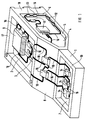
- the injection molded part 1 has a plurality of placement levels 2 to 8.
- conductor tracks 16 Both the production of the injection molded part and the application of the conductor tracks 16 and the fitting of a circuit carrier with components 9 to 15 are carried out in a manner known per se.
- the placement levels can be arranged very freely.
- the placement levels 2 and 3 are arranged one above the other.
- the placement level 4 is arranged at an angle of 90 ° to all other placement levels 2, 3, 5 to 8.
- the placement levels 2 to 7 are sunk, that is to say arranged in the interior of the plastic part 1.
- the placement levels 2 to 7 are so far sunk into the injection molding 1 that the highest of the components 9 to 14 do not protrude beyond the boundary levels 17 to 19.
- another one-piece circuit carrier which is initially electrically insulating on its surface can also be used, for.
Abstract
Description
Die vorliegende Erfindung betrifft ein einstückiges Isolierteil, z. B. ein Kunststoffteil, insbesondere ein Spritzgießteil, mit auf dem Isolierteil angeordneten Leiterzügen. Ein derartiges Isolierteil ist beispielsweise aus der EP-0 465 692 A1 bekannt. Auch beim Automatisierungsgerät SIMATIC S5-95 U der Siemens AG wird ein derartiges Isolierteil als Gehäuserückwand verwendet.The present invention relates to a one-piece insulating part, for. B. a plastic part, in particular an injection molded part, with conductor tracks arranged on the insulating part. Such an insulating part is known for example from EP-0 465 692 A1. Such an insulating part is also used as the rear wall of the housing of the SIMATIC S5-95 U automation device from Siemens AG.
Die bisher bekannten Spritzgießteile mit Leiterzügen waren selbst meist unbestückt, wurden z. B. nur als Rückwandbus verwendet. Übliche Leiterplatten dagegen sind flächig ausgebildet, können also höchstens auf ihrer Vorder- und ihrer Rückseite bestückt werden. Beim Aufbau der Schaltung bleibt daher ein relativ großes Volumen ungenutzt. Die Schaltungen sind also relativ groß.The previously known injection molded parts with conductor tracks were mostly empty, z. B. only used as backplane bus. Conventional printed circuit boards, on the other hand, are flat, so they can only be fitted on the front and back. A relatively large volume therefore remains unused in the construction of the circuit. The circuits are therefore relatively large.
Die Aufgabe der vorliegenden Erfindung besteht darin, die Volumenausnutzung zu vergrößern, so daß im Ergebnis kleinere Schaltungen, z. B. kleinere Steuerungen, realisiert werden können.The object of the present invention is to increase the volume utilization, so that as a result smaller circuits, e.g. B. smaller controls can be realized.
Die Aufgabe wird dadurch gelöst, daß auf dem Isolierteil in mindestens zwei Bestückebenen elektrische und/oder elektronische Bauelemente anordenbar sind, die über die auf dem Isolierteil angeordneten Leiterzüge elektrisch leitend verbunden sind.The object is achieved in that electrical and / or electronic components can be arranged on the insulating part in at least two assembly levels, which are electrically conductively connected via the conductor tracks arranged on the insulating part.
Durch die Verwendung eines dreidimensionalen Isolierteils werden darüber hinaus zusätzliche Topologiefreiheitsgrade ermöglicht, so daß einfachere Leitungsführungen als bei Leiterplatten möglich sind.By using a three-dimensional insulating part, additional topology degrees of freedom are achieved enables so that simpler cable routing than with printed circuit boards are possible.
Weitere Vorteile und Einzelheiten ergeben sich aus der nachfolgenden Beschreibung eines Ausführungsbeispiels, anhand der Zeichnungen und in Verbindung mit den Unteransprüchen. Dabei zeigen:
- FIG 1
- ein erfindungsgemäßes Spritzgießteil in perspektivischer Darstellung und
- FIG 2
- ein Detail eines Spritzgießteils.
- FIG. 1
- an injection molded part according to the invention in a perspective view and
- FIG 2
- a detail of an injection molded part.
Gemäß FIG 1 weist das Spritzgießteil 1 eine Vielzahl von Bestückebenen 2 bis 8 auf. In den Bestückebenen 2 bis 8 sind Bauelemente 9 bis 15, z. B. ICs, Widerstände, Dioden oder Relais, angeordnet, die über Leiterzüge 16 elektrisch leitend miteinander verbunden sind. Sowohl die Herstellung des Spritzgießteils als auch das Aufbringen der Leiterzüge 16 als auch das Bestücken eines Schaltungsträgers mit Bauelementen 9 bis 15 erfolgt dabei in an sich bekannter Weise.According to FIG 1, the injection molded
Wie aus FIG 1 ersichtlich ist, können die Bestückebenen sehr frei angeordnet werden. Beispielsweise sind die Bestückebenen 2 und 3 übereinander angeordnet. Die Bestückebene 4 dagegen ist im Winkel von 90° zu allen anderen Bestückebenen 2, 3, 5 bis 8 angeordnet.As can be seen from FIG. 1, the placement levels can be arranged very freely. For example, the
Zum Schutz der Bauelemente 9 bis 14 vor Beschädigung sind die Bestückebenen 2 bis 7 versenkt, also im Inneren des Kunststoffteils 1 angeordnet. Die Bestückebenen 2 bis 7 sind dabei soweit in das Spritzgießteil 1 hineinversenkt, daß die höchsten der Bauelemente 9 bis 14 die Begrenzungsebenen 17 bis 19 nicht überragen.To protect the components 9 to 14 from damage, the placement levels 2 to 7 are sunk, that is to say arranged in the interior of the
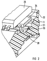
Gemäß FIG 2 können nicht nur zwei, sondern auch drei und mehr Bestückebenen 20 bis 22 übereinander angeordnet werden. In diesem Fall sind selbstverständlich auch drei Schichten von Bauelementen 23 bis 25 vorhanden.According to FIG. 2, not only two, but also three and
Anstelle eines Spritzgießteils kann auch ein anderer einstückiger, auf seiner Oberfläche zunächst elektrisch isolierender Schaltungsträger verwendet werden, z. B. ein auf seiner gesamten Oberfläche in geeigneter Weise eloxiertes Aluminium-Druckgußteil.Instead of an injection molded part, another one-piece circuit carrier which is initially electrically insulating on its surface can also be used, for. B. an appropriately anodized aluminum die-cast part on its entire surface.
Claims (5)
Applications Claiming Priority (2)
| Application Number | Priority Date | Filing Date | Title |
|---|---|---|---|
| DE9300867U | 1993-01-22 | ||
| DE9300867U DE9300867U1 (en) | 1993-01-22 | 1993-01-22 | One-piece insulating part, in particular injection molded part |
Publications (1)
| Publication Number | Publication Date |
|---|---|
| EP0607844A1 true EP0607844A1 (en) | 1994-07-27 |
Family
ID=6888463
Family Applications (1)
| Application Number | Title | Priority Date | Filing Date |
|---|---|---|---|
| EP94100304A Withdrawn EP0607844A1 (en) | 1993-01-22 | 1994-01-11 | One piece insulating part, especially injection molded part |
Country Status (3)
| Country | Link |
|---|---|
| EP (1) | EP0607844A1 (en) |
| JP (1) | JPH06244566A (en) |
| DE (1) | DE9300867U1 (en) |
Cited By (2)
| Publication number | Priority date | Publication date | Assignee | Title |
|---|---|---|---|---|
| DE10104413A1 (en) * | 2001-02-01 | 2002-08-29 | Hella Kg Hueck & Co | Switch has components mounted on circuit bearer on inside of at least one U-shaped bearer arm and/or on inside of bridge connecting bearer arms |
| WO2003086034A1 (en) * | 2002-04-11 | 2003-10-16 | Koninklijke Philips Electronics N.V. | Electrically insulating body, and electronic device |
Families Citing this family (4)
| Publication number | Priority date | Publication date | Assignee | Title |
|---|---|---|---|---|
| DE19708210C2 (en) * | 1997-02-28 | 2003-01-30 | Inter Control Koehler Hermann | Controllers, especially temperature controllers such as room temperature controllers |
| JP3063709B2 (en) | 1997-11-05 | 2000-07-12 | 日本電気株式会社 | Electronic component mounting structure, mounting substrate and electronic component mounting method |
| DE19811901C1 (en) * | 1998-03-18 | 1999-12-02 | Polycontact Ag Chur | Electronic component, esp. sensors, e.g. for control and monitoring |
| DE10152137A1 (en) * | 2001-10-23 | 2003-05-08 | Trw Automotive Electron & Comp | Electronic module and method for its manufacture |
Citations (4)
| Publication number | Priority date | Publication date | Assignee | Title |
|---|---|---|---|---|
| US3346775A (en) * | 1965-06-19 | 1967-10-10 | Interlego Ag | Components for making structures comprising electrical circuits |
| US3427715A (en) * | 1966-06-13 | 1969-02-18 | Motorola Inc | Printed circuit fabrication |
| EP0333550A1 (en) * | 1988-03-11 | 1989-09-20 | Thomson-Csf | Process for producing printed circuits on a three-dimensional plastic carrier, and carrier so equipped |
| EP0465692A1 (en) * | 1990-07-09 | 1992-01-15 | Siemens Aktiengesellschaft | Circuit support |
-
1993
- 1993-01-22 DE DE9300867U patent/DE9300867U1/en not_active Expired - Lifetime
-
1994
- 1994-01-11 EP EP94100304A patent/EP0607844A1/en not_active Withdrawn
- 1994-01-19 JP JP2000694A patent/JPH06244566A/en not_active Withdrawn
Patent Citations (4)
| Publication number | Priority date | Publication date | Assignee | Title |
|---|---|---|---|---|
| US3346775A (en) * | 1965-06-19 | 1967-10-10 | Interlego Ag | Components for making structures comprising electrical circuits |
| US3427715A (en) * | 1966-06-13 | 1969-02-18 | Motorola Inc | Printed circuit fabrication |
| EP0333550A1 (en) * | 1988-03-11 | 1989-09-20 | Thomson-Csf | Process for producing printed circuits on a three-dimensional plastic carrier, and carrier so equipped |
| EP0465692A1 (en) * | 1990-07-09 | 1992-01-15 | Siemens Aktiengesellschaft | Circuit support |
Cited By (2)
| Publication number | Priority date | Publication date | Assignee | Title |
|---|---|---|---|---|
| DE10104413A1 (en) * | 2001-02-01 | 2002-08-29 | Hella Kg Hueck & Co | Switch has components mounted on circuit bearer on inside of at least one U-shaped bearer arm and/or on inside of bridge connecting bearer arms |
| WO2003086034A1 (en) * | 2002-04-11 | 2003-10-16 | Koninklijke Philips Electronics N.V. | Electrically insulating body, and electronic device |
Also Published As
| Publication number | Publication date |
|---|---|
| DE9300867U1 (en) | 1994-05-26 |
| JPH06244566A (en) | 1994-09-02 |
Similar Documents
| Publication | Publication Date | Title |
|---|---|---|
| DE3942392C2 (en) | Electronic control device for a motor vehicle | |
| DE3511722A1 (en) | ELECTROMECHANICAL ASSEMBLY FOR INTEGRATED CIRCUIT MATRICES | |
| DE1936568U (en) | ELECTRICAL CONNECTION DEVICE. | |
| DE4415200C1 (en) | Computer component assembly | |
| EP0607844A1 (en) | One piece insulating part, especially injection molded part | |
| EP0607846A1 (en) | One piece plastic part, especially injection molded part | |
| DE1942839A1 (en) | Pluggable board with printed circuit | |
| DE4016953A1 (en) | Electronic device with electromagnetic screening - using insulating and conductive pref. epoxy¨ resin layers | |
| DE3731413A1 (en) | Electrical switching apparatus | |
| DE4106453C1 (en) | ||
| EP0607843B1 (en) | One piece insulating part, especially injection molded part | |
| DE2904012A1 (en) | Support rack for protective retention of printed circuit boards - has board retaining capsules with terminal blocks and external terminals for connecting outer lines | |
| EP0283677B1 (en) | Electrical construction unit | |
| DE4300899A1 (en) | Array of mounted electronic components | |
| EP0093080B1 (en) | Keyboard | |
| DE1059988B (en) | Electrical assembly | |
| DE3323029A1 (en) | DEVICE FOR CONNECTING CABLES TO CONNECTING PCBS | |
| DE7600991U1 (en) | Housing for a single flat module | |
| EP0607845A1 (en) | One piece insulating part, especially injection molded part | |
| DE2261106C2 (en) | Electrical assembly with a housing | |
| DE2813812A1 (en) | Rack for withdrawable electric or electronic modules - has separate wirings intrinsically safe and non-safe areas separated by insulating hood | |
| DE19717909A1 (en) | Electric device | |
| EP0818947A1 (en) | Spacer for boards | |
| DE10030289B4 (en) | Carrier for components and manufacturing processes | |
| DE19607194A1 (en) | Potted, PCB-less electrical / electronic assembly |
Legal Events
| Date | Code | Title | Description |
|---|---|---|---|
| PUAI | Public reference made under article 153(3) epc to a published international application that has entered the european phase |
Free format text: ORIGINAL CODE: 0009012 |
|
| AK | Designated contracting states |
Kind code of ref document: A1 Designated state(s): AT CH DE FR GB IT LI NL SE |
|
| 17P | Request for examination filed |
Effective date: 19940826 |
|
| 17Q | First examination report despatched |
Effective date: 19950222 |
|
| STAA | Information on the status of an ep patent application or granted ep patent |
Free format text: STATUS: THE APPLICATION IS DEEMED TO BE WITHDRAWN |
|
| 18D | Application deemed to be withdrawn |
Effective date: 19950705 |