EP0614218A1 - Method for manufacturing capacitor and MIS transistor - Google Patents
Method for manufacturing capacitor and MIS transistor Download PDFInfo
- Publication number
- EP0614218A1 EP0614218A1 EP94301461A EP94301461A EP0614218A1 EP 0614218 A1 EP0614218 A1 EP 0614218A1 EP 94301461 A EP94301461 A EP 94301461A EP 94301461 A EP94301461 A EP 94301461A EP 0614218 A1 EP0614218 A1 EP 0614218A1
- Authority
- EP
- European Patent Office
- Prior art keywords
- forming
- layer
- capacitor
- forming area
- mis transistor
- Prior art date
- Legal status (The legal status is an assumption and is not a legal conclusion. Google has not performed a legal analysis and makes no representation as to the accuracy of the status listed.)
- Withdrawn
Links
Images


Classifications
-
- H—ELECTRICITY
- H01—ELECTRIC ELEMENTS
- H01L—SEMICONDUCTOR DEVICES NOT COVERED BY CLASS H10
- H01L27/00—Devices consisting of a plurality of semiconductor or other solid-state components formed in or on a common substrate
- H01L27/02—Devices consisting of a plurality of semiconductor or other solid-state components formed in or on a common substrate including semiconductor components specially adapted for rectifying, oscillating, amplifying or switching and having at least one potential-jump barrier or surface barrier; including integrated passive circuit elements with at least one potential-jump barrier or surface barrier
- H01L27/04—Devices consisting of a plurality of semiconductor or other solid-state components formed in or on a common substrate including semiconductor components specially adapted for rectifying, oscillating, amplifying or switching and having at least one potential-jump barrier or surface barrier; including integrated passive circuit elements with at least one potential-jump barrier or surface barrier the substrate being a semiconductor body
- H01L27/06—Devices consisting of a plurality of semiconductor or other solid-state components formed in or on a common substrate including semiconductor components specially adapted for rectifying, oscillating, amplifying or switching and having at least one potential-jump barrier or surface barrier; including integrated passive circuit elements with at least one potential-jump barrier or surface barrier the substrate being a semiconductor body including a plurality of individual components in a non-repetitive configuration
- H01L27/0611—Devices consisting of a plurality of semiconductor or other solid-state components formed in or on a common substrate including semiconductor components specially adapted for rectifying, oscillating, amplifying or switching and having at least one potential-jump barrier or surface barrier; including integrated passive circuit elements with at least one potential-jump barrier or surface barrier the substrate being a semiconductor body including a plurality of individual components in a non-repetitive configuration integrated circuits having a two-dimensional layout of components without a common active region
- H01L27/0617—Devices consisting of a plurality of semiconductor or other solid-state components formed in or on a common substrate including semiconductor components specially adapted for rectifying, oscillating, amplifying or switching and having at least one potential-jump barrier or surface barrier; including integrated passive circuit elements with at least one potential-jump barrier or surface barrier the substrate being a semiconductor body including a plurality of individual components in a non-repetitive configuration integrated circuits having a two-dimensional layout of components without a common active region comprising components of the field-effect type
- H01L27/0629—Devices consisting of a plurality of semiconductor or other solid-state components formed in or on a common substrate including semiconductor components specially adapted for rectifying, oscillating, amplifying or switching and having at least one potential-jump barrier or surface barrier; including integrated passive circuit elements with at least one potential-jump barrier or surface barrier the substrate being a semiconductor body including a plurality of individual components in a non-repetitive configuration integrated circuits having a two-dimensional layout of components without a common active region comprising components of the field-effect type in combination with diodes, or resistors, or capacitors
-
- H—ELECTRICITY
- H10—SEMICONDUCTOR DEVICES; ELECTRIC SOLID-STATE DEVICES NOT OTHERWISE PROVIDED FOR
- H10B—ELECTRONIC MEMORY DEVICES
- H10B12/00—Dynamic random access memory [DRAM] devices
- H10B12/01—Manufacture or treatment
- H10B12/02—Manufacture or treatment for one transistor one-capacitor [1T-1C] memory cells
- H10B12/03—Making the capacitor or connections thereto
- H10B12/033—Making the capacitor or connections thereto the capacitor extending over the transistor
Definitions
- the present invention relates to a method for manufacturing a semiconductor device, and more particularly, to a method for manufacturing a capacitor and a metal oxide semiconductor (MOS, broadly, a metal insulating semiconductor (MIS)) transistor on the same semiconductor substrate.
- MOS metal oxide semiconductor
- MIS metal insulating semiconductor
- a capacitor including lower and upper electrodes and a dielectric layer therebetween is formed on a thick insulating layer, i.e., a so-called field insulating layer which defines a field area, to thereby increase the capacity of the capacitor.
- a MOS transistor is formed on an active area where the field insulating layer is not formed.
- the lower electrode is formed; the dielectric layer is formed; and afterwards, the upper electrode is formed simultaneously with a gate electrode of the MIS transistor. Thereafter, impurities are doped by an ion implantation into a semiconductor substrate to form source and drain regions within the semiconductor substrate.
- the upper electrode of the capacitor is covered with a photoresist layer, thus avoiding the introduction of impurities into the upper electrode. If such impurities are doped into the upper electrode, the impurities may reach an interface between the upper electrode and the dielectric layer, to thereby reduce the duration of the capacitor and increase the leakage current of the capacitor, thus deteriorating the reliability of the semiconductor device.
- the concentration of impurities in the upper electrode which is made of polycrystalline silicon, for example, is quite low, a depletion region may appear within the upper electrode in response to a voltage applied thereto. As a result, a capacity resulting from this depletion region is connected in series to an original capacity of the dielectric layer, to thereby substantially reduce the capacity of the capacitor.
- the capacity of the capacitor manufactured by the prior art method has a dependency on voltage applied thereto, and also it is difficult to suppress the voltage dependency below a level such as 0.05%/V required in a highly-defined analog circuit.
- impurity ions are introduced by ion implantation into the upper electrode, as well as into a gate electrode of the MIS transistor.
- a depletion region is hardly generated within the upper electrode, and therefore, the capacitor has no dependency on voltage applied thereto.
- Figs. 1 through 14 are cross-sectional views for explaining an embodiment of the method for manufacturing a capacitor, an N-channel MOS transistor and a P-channel MOS transistor according to the present invention.
- a reference C designates a capacitor forming area
- Q n designates an N-channel MOS transistor forming area
- Q p designates a P-channel MOS transistor forming area.
- a P-type monocrystalline silicon substrate 1 is prepared, and the silicon substrate 1 is oxidized in a steam atmosphere at a temperature of about 980°C to form an approximately 480 nm thick silicon oxide layer 2. Then, a part of the silicon oxide layer 2 at the P-channel MOS transistor area Q p is etched out by using a photolithography process, and afterward, the silicon substrate 1 is grown thermally at a temperature of about 950°C. to thereby form an approximately 45 nm thick silicon oxide layer 3.
- N-type impurity ions such as phosphorus ions/cm2 at an energy of 150keV are doped by an ion implantation process to form an N-type well 4 within the silicon substrate 1.
- the silicon oxide layers 2 and 3 are etched out.
- the silicon substrate 1 is again grown thermally at a temperature of about 950°C. to form an approximately 60 nm thick silicon oxide layer 5.
- an approximately 120 nm thick silicon nitride layer 6 is formed by a chemical vapor deposition(CVD) process, and the silicon nitride layer 6 is etched out by a photolithography process, so that the silicon nitride layer 6 remains only on the N-channel MOS transistor forming area Q n and the P-channel MOS transistor forming area Q p which are so-called active areas.
- CVD chemical vapor deposition
- LOCS local oxidation of silicon
- the silicon nitride layer 6 is removed.
- an approximately 400 nm thick polycrystalline silicon layer is formed by a CVD process, and a heat operation is carried out, to dope N-type impurities such as phosphorus thereinto, so that the sheet resistance thereof is about 40 ⁇ / ⁇ .
- the phosphorus doped polycrystalline silicon layer is patterned by a photolithography process, to obtain a capacitor lower electrode 8.
- an approximately 17 nm thick silicon oxide layer 91 is formed by thermally growing the capacitor lower electrode (polycrystalline silicon) 8. Then, an approximately 20 nm thick silicon nitride layer 92 is formed on the entire surface by a CVD process, and the silicon nitride layer 92 is oxidized to grow a several nm thick silicon oxide layer 93 thereon.
- the silicon oxide layer 93 and the silicon nitride layer 92 are patterned by a photolithography process, to form a capacitor dielectric layer of a triple layer configuration including the silicon oxide layer 91, the silicon nitride layer 92 and the silicon oxide layer 93. Then, the silicon oxide layer 5 is removed, and an approximately 16 nm thick silicon oxide layer 10 is again formed by thermally growing the MOS transistor forming areas Q n and Q p of the silicon substrate 1.
- an approximately 150 nm thick polycrystalline silicon layer 11 is formed on the entire surface by a CVD process, and a heat operation is carried out to dope N-type impurities such as phosphorus thereinto, so that the sheet resistance thereof is about 40 ⁇ / ⁇ . Also, in order to enhance the operation speed of the transistors, an approximately 150 nm thick tungsten silicide layer 12 is formed on the entire surface by a sputtering process.
- the polycrystalline silicon layer 11 and the tungsten silicide layer 12 are patterned by a photolithography process, to obtain a polycrystalline silicon layer 11A and a tungsten silicide layer 12A for a capacitor upper electrode in the capacitor forming area C, a polycrystalline silicon layer 11B and a tungsten silicide layer 12B for a gate electrode in the N-channel MOS transistor forming area Q n , and a polycrystalline silicon layer 11C and a tungsten silicide layer 12C for a gate electrode in the P-channel MOS transistor forming area Q p .
- the resistance of these gate electrodes is made low by a double layer configuration comprised of polycrystalline silicon and tungsten silicide.
- the P-channel MOS transistor forming area Q p is covered with a photoresist pattern 13.
- 1015 N-type impurity ions, such as arsenic ions, per cm2 at an energy of 70 keV are doped into the silicon substrate 1, to form a source region 14S and a drain region 14D within the silicon substrate 1.
- the source region 14S and the drain region 14D have an impurity concentration of about 1020 arsenic ions/cm3.
- impurity ions are doped into the tungsten silicide layer 12A and the polycrystalline silicon layer 11A as well as the tungsten silicide layer 12B and the polycrystalline silicon layer 11B.
- the photoresist pattern 13 is removed.
- the capacitor forming area C and the N-channel MOS transistor forming area Q n are covered with another photoresist pattern 15.
- 5 ⁇ 1015 P-type impurity ions, such as boron ions, per cm2 at an energy of 30 keV are doped into the silicon substrate 1, to form a source region 16S and a drain region 16D within the silicon substrate 1.
- the source region 16S and the drain region 16D have an impurity concentration of about 5x ⁇ 1020 boron ions/cm3.
- a heating or annealling process is carried out under an atmosphere of nitrogen at a temperature of about 950°C for approximately 30 minutes.
- the doped impurity ions are more deeply penetrated into the polycrystalline silicon layers 11A, 11B and 11C as well as the regions 14S, 14D, 16S and 16D.
- the lattice arrangement of polycrystalline silicon and monocrystalline silicon damaged by the above-mentioned implantation of ions is repaired, and also, the doped ions are arranged uniformly within the polycrystalline silicon and monocrystalline silicon to activate them. Note that this heating or annealling process contributes to enhancement of the concentration of impurities within the capacitor upper electrode formed by the polycrystalline silicon layer 11A and the tungsten silicide layer 12A.
- an approximately 150 nm thick silicon oxide layer 17 is formed by a CVD process on the entire surface, and an approximately 650 nm thick boron-doped phospho-silicated glass(BPSG) layer 18 is formed by a CVD process.
- a heating process is carried out in an atmosphere of nitrogen at a temperature of about 900°C to improve the coverage characteristics of the silicon oxide layer 17 and the BPSG layer 18.
- contact holes 19A, 19B, 19C and 19D are provided for ohmic contact with connection lines (not shown) made of aluminium and tungsten silicide.
- Figs. 13 and 14 which are modifications of Figs. 10 and 11, respectively, photoresist patterns 13' and 15' are provided instead of the photoresist patterns 13 and 15. That is, the photoresist pattern 13' covers the capacitor upper electrode formed by the polycrystalline silicon layer 11A and the tungsten silicide layer 12A as illustrated in Fig. 13, while the photoresist pattern 15' does not cover the capacitor upper electrode formed by the polycrystalline silicon layer 11A and the tungsten silicide layer 12A as illustrated in Fig. 14. Therefore, the P-type impurity ions such as boron ions are doped by ion implantation into the capacitor upper electrode.
- the P-type impurity ions such as boron ions are doped by ion implantation into the capacitor upper electrode.
- the type of impurity ions doped by ion implantation depends upon the direction of a bias voltage applied to the capacitor. For example, if a negative voltage is applied to the capacitor upper electrode and a positive voltage is applied to the capacitor lower electrode, N-type impurity ions are implanted into the capacitor upper electrode. Conversely, if a positive voltage is applied to the capacitor upper electrode and a negative voltage is applied to the capacitor lower electrode, P-type impurity ions are implanted into the capacitor upper electrode.
- the silicon oxide layer 93 obtained by thermally growing the silicon nitride layer 92 improves the property of the silicon nitride layer 92, so as to enhance the duration of the capacitor dielectric layer and reduce the leakage current therethrough.
- the introduction of impurities by ion implantation into the capacitor upper electrode neither deteriorates the property of the capacitor dielectric layer, nor increases the leakage current therethrough.
- the duration of the capacitor dielectric layer is higher than 20V, and the leakage current therethrough is less than 1 nA.
- the capacitor dielectric layer is not reduced in reliability.
- a capacitor manufactured by the present invention has a capacity of about 10 nF in the case of an area of 3.5mm2. Also, in a range of 0 to 5V, the voltage dependency, i.e., the difference in capacity between each voltage and a zero bias voltage is about 0.01%/V according to the present invention, while 0.04%/V in the prior art. That is, the voltage dependency obtained by using the manufacturing method according to the present invention can satisfy the specification 0.05%/V required in a highly defined analog circuit.
Abstract
In a method for manufacturing a capacitor (C) having a lower electrode (8), an upper electrode (11A, 12A) and a dielectric layer (91, 92, 93) therebetween and a MIS transistor (Qn, QP) on the same semiconductor substrate (1), impurity ions are introduced by ion implantation into the upper electrode as well as a gate electrode of the MIS transistor.
Description
- The present invention relates to a method for manufacturing a semiconductor device, and more particularly, to a method for manufacturing a capacitor and a metal oxide semiconductor (MOS, broadly, a metal insulating semiconductor (MIS)) transistor on the same semiconductor substrate.
- Generally, in a highly-functional and highly-defined semiconductor device, a capacitor including lower and upper electrodes and a dielectric layer therebetween is formed on a thick insulating layer, i.e., a so-called field insulating layer which defines a field area, to thereby increase the capacity of the capacitor. Also, a MOS transistor is formed on an active area where the field insulating layer is not formed.
- In the prior art, when manufacturing the above-mentioned capacitor and the MOS transistor, the lower electrode is formed; the dielectric layer is formed; and afterwards, the upper electrode is formed simultaneously with a gate electrode of the MIS transistor. Thereafter, impurities are doped by an ion implantation into a semiconductor substrate to form source and drain regions within the semiconductor substrate.
- In the prior art, however, when doping impurities into the semiconductor substrate to form the source and drain regions, the upper electrode of the capacitor is covered with a photoresist layer, thus avoiding the introduction of impurities into the upper electrode. If such impurities are doped into the upper electrode, the impurities may reach an interface between the upper electrode and the dielectric layer, to thereby reduce the duration of the capacitor and increase the leakage current of the capacitor, thus deteriorating the reliability of the semiconductor device.
- In the capacitor manufactured by the above-mentioned prior art manufacturing method, however, since the concentration of impurities in the upper electrode, which is made of polycrystalline silicon, for example, is quite low, a depletion region may appear within the upper electrode in response to a voltage applied thereto. As a result, a capacity resulting from this depletion region is connected in series to an original capacity of the dielectric layer, to thereby substantially reduce the capacity of the capacitor.
- Thus, the capacity of the capacitor manufactured by the prior art method has a dependency on voltage applied thereto, and also it is difficult to suppress the voltage dependency below a level such as 0.05%/V required in a highly-defined analog circuit.
- It is an object of the present invention to suppress the voltage dependency of the capacity of a capacitor manufactured on the same semiconductor substrate on which a MIS transistor is formed.
- According to the present invention, in a method for manufacturing a capacitor having a lower electrode, an upper electrode and a dielectric layer therebetween, and a MIS transistor on the same semiconductor substrate, impurity ions are introduced by ion implantation into the upper electrode, as well as into a gate electrode of the MIS transistor. As a result, a depletion region is hardly generated within the upper electrode, and therefore, the capacitor has no dependency on voltage applied thereto.
- The present invention will be more clearly understood from the description as set forth below with reference to the accompanying drawings, wherein:
Figs. 1 through 14 are cross-sectional views for explaining an embodiment of the method for manufacturing a capacitor, an N-channel MOS transistor and a P-channel MOS transistor according to the present invention. - In Figs. 1 through 12, a reference C designates a capacitor forming area; Qn designates an N-channel MOS transistor forming area; and Qp designates a P-channel MOS transistor forming area.
- As illustrated in Fig. 1, a P-type
monocrystalline silicon substrate 1 is prepared, and thesilicon substrate 1 is oxidized in a steam atmosphere at a temperature of about 980°C to form an approximately 480 nm thicksilicon oxide layer 2. Then, a part of thesilicon oxide layer 2 at the P-channel MOS transistor area Qp is etched out by using a photolithography process, and afterward, thesilicon substrate 1 is grown thermally at a temperature of about 950°C. to thereby form an approximately 45 nm thicksilicon oxide layer 3. - Next, as illustrated in Fig. 2, about 2.1×10¹³ N-type impurity ions such as phosphorus ions/cm² at an energy of 150keV are doped by an ion implantation process to form an N-
type well 4 within thesilicon substrate 1. - Next, as illustrated in Fig. 3, the
silicon oxide layers silicon substrate 1 is again grown thermally at a temperature of about 950°C. to form an approximately 60 nm thicksilicon oxide layer 5. Afterward, an approximately 120 nm thicksilicon nitride layer 6 is formed by a chemical vapor deposition(CVD) process, and thesilicon nitride layer 6 is etched out by a photolithography process, so that thesilicon nitride layer 6 remains only on the N-channel MOS transistor forming area Qn and the P-channel MOS transistor forming area Qp which are so-called active areas. - Next, as illustrated in Fig. 4, local oxidation of silicon (LOCOS) is carried out to form an approximately 600 nm thick silicon oxide layer, i.e., a
field oxide layer 7 for isolating the transistor elements from each other. In this case, thefield oxide layer 7 is also formed in the capacity forming area C. - Next, as illustrated in Fig. 5, the
silicon nitride layer 6 is removed. Then, an approximately 400 nm thick polycrystalline silicon layer is formed by a CVD process, and a heat operation is carried out, to dope N-type impurities such as phosphorus thereinto, so that the sheet resistance thereof is about 40 Ω/□. Then, the phosphorus doped polycrystalline silicon layer is patterned by a photolithography process, to obtain a capacitorlower electrode 8. - Next, as illustrated in Fig. 6, an approximately 17 nm thick
silicon oxide layer 91 is formed by thermally growing the capacitor lower electrode (polycrystalline silicon) 8. Then, an approximately 20 nm thicksilicon nitride layer 92 is formed on the entire surface by a CVD process, and thesilicon nitride layer 92 is oxidized to grow a several nm thicksilicon oxide layer 93 thereon. - Next, as illustrated in Fig. 7, the
silicon oxide layer 93 and thesilicon nitride layer 92 are patterned by a photolithography process, to form a capacitor dielectric layer of a triple layer configuration including thesilicon oxide layer 91, thesilicon nitride layer 92 and thesilicon oxide layer 93. Then, thesilicon oxide layer 5 is removed, and an approximately 16 nm thicksilicon oxide layer 10 is again formed by thermally growing the MOS transistor forming areas Qn and Qp of thesilicon substrate 1. - Next, as illustrated in Fig. 8, an approximately 150 nm thick
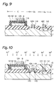
polycrystalline silicon layer 11 is formed on the entire surface by a CVD process, and a heat operation is carried out to dope N-type impurities such as phosphorus thereinto, so that the sheet resistance thereof is about 40 Ω/□. Also, in order to enhance the operation speed of the transistors, an approximately 150 nm thicktungsten silicide layer 12 is formed on the entire surface by a sputtering process. - Next, as illustrated in Fig. 9, the
polycrystalline silicon layer 11 and thetungsten silicide layer 12 are patterned by a photolithography process, to obtain apolycrystalline silicon layer 11A and atungsten silicide layer 12A for a capacitor upper electrode in the capacitor forming area C, apolycrystalline silicon layer 11B and atungsten silicide layer 12B for a gate electrode in the N-channel MOS transistor forming area Qn, and apolycrystalline silicon layer 11C and atungsten silicide layer 12C for a gate electrode in the P-channel MOS transistor forming area Qp. Note that the resistance of these gate electrodes is made low by a double layer configuration comprised of polycrystalline silicon and tungsten silicide. - Next, as illustrated in Fig. 10, the P-channel MOS transistor forming area Qp is covered with a
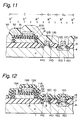
photoresist pattern 13. Then, 10¹⁵ N-type impurity ions, such as arsenic ions, per cm² at an energy of 70 keV are doped into thesilicon substrate 1, to form asource region 14S and adrain region 14D within thesilicon substrate 1. As a result, thesource region 14S and thedrain region 14D have an impurity concentration of about 10²⁰ arsenic ions/cm³. In this case, such impurity ions are doped into thetungsten silicide layer 12A and thepolycrystalline silicon layer 11A as well as thetungsten silicide layer 12B and thepolycrystalline silicon layer 11B. Then, thephotoresist pattern 13 is removed. - Next, as illustrated in Fig. 11, the capacitor forming area C and the N-channel MOS transistor forming area Qn are covered with another
photoresist pattern 15. Then, 5×10¹⁵ P-type impurity ions, such as boron ions, per cm² at an energy of 30 keV are doped into thesilicon substrate 1, to form asource region 16S and adrain region 16D within thesilicon substrate 1. As a result, thesource region 16S and thedrain region 16D have an impurity concentration of about 5x×10²⁰ boron ions/cm³. In this case, such impurity ions are not doped into thetungsten silicide layer 12A and thepolycrystalline silicon layer 11A, thetungsten silicide layer 12B and thepolycrystalline silicon layer 11B. Then, thephotoresist pattern 15 is removed. - Next, a heating or annealling process is carried out under an atmosphere of nitrogen at a temperature of about 950°C for approximately 30 minutes. As a result, the doped impurity ions are more deeply penetrated into the
polycrystalline silicon layers regions polycrystalline silicon layer 11A and thetungsten silicide layer 12A. - Next, as illustrated in Fig. 12, an approximately 150 nm thick
silicon oxide layer 17 is formed by a CVD process on the entire surface, and an approximately 650 nm thick boron-doped phospho-silicated glass(BPSG)layer 18 is formed by a CVD process. Then, a heating process is carried out in an atmosphere of nitrogen at a temperature of about 900°C to improve the coverage characteristics of thesilicon oxide layer 17 and theBPSG layer 18. After that,contact holes - In Figs. 13 and 14, which are modifications of Figs. 10 and 11, respectively, photoresist patterns 13' and 15' are provided instead of the
photoresist patterns polycrystalline silicon layer 11A and thetungsten silicide layer 12A as illustrated in Fig. 13, while the photoresist pattern 15' does not cover the capacitor upper electrode formed by thepolycrystalline silicon layer 11A and thetungsten silicide layer 12A as illustrated in Fig. 14. Therefore, the P-type impurity ions such as boron ions are doped by ion implantation into the capacitor upper electrode. - The type of impurity ions doped by ion implantation depends upon the direction of a bias voltage applied to the capacitor. For example, if a negative voltage is applied to the capacitor upper electrode and a positive voltage is applied to the capacitor lower electrode, N-type impurity ions are implanted into the capacitor upper electrode. Conversely, if a positive voltage is applied to the capacitor upper electrode and a negative voltage is applied to the capacitor lower electrode, P-type impurity ions are implanted into the capacitor upper electrode.
- Note that, in the capacitor dielectric layer comprised of a triple layer configuration, the
silicon oxide layer 93 obtained by thermally growing thesilicon nitride layer 92 improves the property of thesilicon nitride layer 92, so as to enhance the duration of the capacitor dielectric layer and reduce the leakage current therethrough. - Also, according to an experimental implementation by the inventor, the introduction of impurities by ion implantation into the capacitor upper electrode neither deteriorates the property of the capacitor dielectric layer, nor increases the leakage current therethrough. For example, the duration of the capacitor dielectric layer is higher than 20V, and the leakage current therethrough is less than 1 nA. Thus, the capacitor dielectric layer is not reduced in reliability.
- Also, according to another experimental implementation by the inventor, a capacitor manufactured by the present invention has a capacity of about 10 nF in the case of an area of 3.5mm². Also, in a range of 0 to 5V, the voltage dependency, i.e., the difference in capacity between each voltage and a zero bias voltage is about 0.01%/V according to the present invention, while 0.04%/V in the prior art. That is, the voltage dependency obtained by using the manufacturing method according to the present invention can satisfy the specification 0.05%/V required in a highly defined analog circuit.
- As explained hereinbefore, according to the present invention, since impurity ions are introduced by ion implantation into a capacitor upper electrode, a depletion region is hardly generated within the capacitor upper electrode, so that the voltage dependency of the capacity of a capacitor can be suppressed.
Claims (15)
- A method for manufacturing a capacitor and a MIS transistor by using a semiconductor substrate (1) including a capacitor forming area (C) and a MIS transistor forming area (Qn, Qp), comprising the steps of:
forming a field insulating layer (7) on the capacitor forming area of said semiconductor substrate;
forming a capacitor lower electrode (8) on said field insulating layer;
forming a capacitor dielectric layer (91, 92, 93) on said capacitor lower electrode;
forming a gate insulating layer (10) on the MIS forming area of said semiconductor substrate;
forming a capacitor upper electrode (11A, 12A) on said capacitor dielectric layer and a gate electrode (11B, 12B, 11C, 12C) on said gate insulating layer; and
introducing impurity ions into said capacitor upper electrode and said gate electrode by ion implantation. - A method as set forth in claim 1, wherein said upper electrode and gate electrode forming step comprises the steps of:
forming a polycrstalline silicon layer (11);
forming a tungsten silicide layer (12) on said polycrystalline silicon layer;
patterning said tungsten silicide layer and said polycrystalline silicon layer, to form said upper electrode and said gate electrode. - A method as set forth in claim 1, wherein said capacitor dielectric layer forming step comprises the steps of:
forming a first silicon oxide layer (91);
forming a silicon nitride layer (92) on said first silicon oxide layer;
forming a second silicon oxide layer (93) on said silicon nitride layer; and
patterning said second silicon oxide layer, said silicon nitride layer and said first silicon oxide layer, to form said capacitor dielectric layer. - A method as set forth in claim 3, wherein said capacitor lower electrode is made of polycrystalline silicon,
said first silicon oxide layer forming step comprising a step of thermally growing said capacitor lower electrode. - A method as set forth in claim 3, wherein said second silicon oxide layer forming step comprises a step of thermally growing said silicon nitride layer.
- A method for manufacturing a capacitor, an N-channel MIS transistor and a P-channel MIS transistor by using a semiconductor substrate (1) including a capacitor forming area (C), an N-channel MIS transistor forming area (Qn) and a P-channel MIS transistor forming area (Qp) comprising the steps of:
forming a field insulating layer (7) on the capacitor forming area of said semiconductor substrate;
forming a capacitor lower electrode (8) on said field insulating layer;
forming a capacitor dielectric layer (91, 92, 93) on said capacitor lower electrode;
forming a gate insulating layer (10) on the N-channel MIS transistor forming area and the P-channel MIS forming area of said semiconductor substrate;
forming a capacitor upper electrode (11A, 12A) on said capacitor dielectric layer, a gate electrode (11B, 12B) on said gate insulating layer of the N-channel MIS transistor forming area and a gate electrode (11C, 12C) on said gate insulating layer of the P-channel MIS transistor forming area;
covering the P-channel MIS transistor forming area with a first photoresist pattern (13);
introducing N-type impurity ions into the capacitor forming area and the N-channel MIS transistor forming area with a mask of said first photoresist pattern by ion implantation;
removing said first photoresist pattern;
covering the capacitor forming area and the N-channel MIS transistor forming area with a second photoresist pattern (15); and
introducing P-type impurity ions into the P-channel MIS forming area with a mask of said second photoresist pattern by ion implantation. - A method as set forth in claim 6, wherein said upper electrode and gate electrode forming step comprises the steps of:
forming a polycrstalline silicon layer (11);
forming a tungsten silicide layer (12) on said polycrystalline silicon layer; and
patterning said tungsten silicide layer and said polycrystalline silicon layer, to form said upper electrode and said gate electrode. - A method as set forth in claim 6, wherein said capacitor dielectric layer forming step comprises the steps of:
forming a first silicon oxide layer (91);
forming a silicon nitride layer (92) on said first silicon oxide layer;
forming a second silicon oxide layer (93) on said silicon nitride layer; and
patterning said second silicon oxide layer, said silicon nitride layer and said first silicon oxide layer, to form said capacitor dielectric layer. - A method as set forth in claim 8, wherein said capacitor lower electrode is made of polycrystalline silicon,
said first silicon oxide layer forming step comprising a step of thermally growing said capacitor lower electrode. - A method as set forth in claim 8, wherein said second silicon oxide layer forming step comprises a step of thermally growing said silicon nitride layer.
- A method for manufacturing a capacitor, an N-channel MIS transistor and a P-channel MIS transistor by using a semiconductor substrate (1) including a capacitor forming area (C), an N-channel MIS transistor forming area (Qn) and a P-channel MIS transistor forming area (Qp), comprising the steps of:
forming a field insulating layer (7) on the capacitor forming area of said semiconductor substrate;
forming a capacitor lower electrode (8) on said field insulating layer;
forming a capacitor dielectric layer (91, 92, 93) on said capacitor lower electrode;
forming a gate insulating layer (10) on the N-channel MIS transistor forming area and the P-channel MIS forming area of said semiconductor substrate;
forming a capacitor upper electrode (11A, 12A) on said capacitor dielectric layer, a gate electrode (11B, 12B) on said gate insulating layer of the N-channel MIS transistor forming area and a gate electrode (11C, 12C) on said gate insulating layer of the P-channel MIS transistor forming area;
covering the capacitor forming area and the P-channel MIS transistor forming area with a first photoresist pattern (13');
introducing N-type impurity ions into the N-channel MIS transistor forming area with a mask of said first photoresist pattern by ion implantation;
removing said first photoresist pattern;
covering the N-channel MIS transistor forming area with a second photoresist pattern (15); and
introducing P-type impurity ions into the capacitor forming area and the P-channel MIS forming area with a mask of said second photoresist pattern by ion implantation. - A method as set forth in claim 6, wherein said upper electrode and gate electrode forming step comprises the steps of:
forming a polycrstalline silicon layer (11);
forming a tungsten silicide layer (12) on said polycrystalline silicon layer; and
patterning said tungsten silicide layer and said polycrystalline silicon layer, to form said upper electrode and said gate electrode. - A method as set forth in claim 11, wherein said capacitor dielectric layer forming step comprises the steps of:
forming a first silicon oxide layer (91);
forming a silicon nitride layer (92) on said first silicon oxide layer;
forming a second silicon oxide layer (93) on said silicon nitride layer; and
patterning said second silicon oxide layer, said silicon nitride layer and said first silicon oxide layer, to form said capacitor dielectric layer. - A method as set forth in claim 13, wherein said capacitor lower electrode is made of polycrystalline silicon,
said first silicon oxide layer forming step comprising a step of thermally growing said capacitor lower electrode. - A method as set forth in claim 13, wherein said second silicon oxide layer forming step comprises a step of thermally growing said silicon nitride layer.
Applications Claiming Priority (2)
| Application Number | Priority Date | Filing Date | Title |
|---|---|---|---|
| JP40801/93 | 1993-03-02 | ||
| JP5040801A JPH06252345A (en) | 1993-03-02 | 1993-03-02 | Manufacture of semiconductor integrated circuit |
Publications (1)
| Publication Number | Publication Date |
|---|---|
| EP0614218A1 true EP0614218A1 (en) | 1994-09-07 |
Family
ID=12590741
Family Applications (1)
| Application Number | Title | Priority Date | Filing Date |
|---|---|---|---|
| EP94301461A Withdrawn EP0614218A1 (en) | 1993-03-02 | 1994-03-01 | Method for manufacturing capacitor and MIS transistor |
Country Status (2)
| Country | Link |
|---|---|
| EP (1) | EP0614218A1 (en) |
| JP (1) | JPH06252345A (en) |
Cited By (1)
| Publication number | Priority date | Publication date | Assignee | Title |
|---|---|---|---|---|
| DE19506155A1 (en) * | 1994-03-01 | 1995-09-07 | Mitsubishi Electric Corp | Semiconductor device with capacitor |
Families Citing this family (4)
| Publication number | Priority date | Publication date | Assignee | Title |
|---|---|---|---|---|
| CN1112731C (en) * | 1997-04-30 | 2003-06-25 | 三星电子株式会社 | Method for making capacitor used for analog function |
| JP3419660B2 (en) * | 1997-10-01 | 2003-06-23 | 沖電気工業株式会社 | Method of forming capacitance section of semiconductor device, and method of forming capacitance section and gate section of semiconductor device |
| KR100258203B1 (en) | 1997-12-29 | 2000-06-01 | 김영환 | Method for manufacturing analog semiconductor device |
| JP2015195337A (en) * | 2014-03-28 | 2015-11-05 | ローム株式会社 | Discrete capacitor and manufacturing method of the same |
Citations (4)
| Publication number | Priority date | Publication date | Assignee | Title |
|---|---|---|---|---|
| US4249194A (en) * | 1977-08-29 | 1981-02-03 | Texas Instruments Incorporated | Integrated circuit MOS capacitor using implanted region to change threshold |
| US4419812A (en) * | 1982-08-23 | 1983-12-13 | Ncr Corporation | Method of fabricating an integrated circuit voltage multiplier containing a parallel plate capacitor |
| EP0435534A2 (en) * | 1989-12-14 | 1991-07-03 | STMicroelectronics S.r.l. | Method of manufacturing integrated circuit and integrated circuit made thereby |
| US5171699A (en) * | 1990-10-03 | 1992-12-15 | Texas Instruments Incorporated | Vertical DMOS transistor structure built in an N-well CMOS-based BiCMOS process and method of fabrication |
Family Cites Families (1)
| Publication number | Priority date | Publication date | Assignee | Title |
|---|---|---|---|---|
| JPH02213158A (en) * | 1989-02-13 | 1990-08-24 | Nec Corp | Manufacture of semiconductor device |
-
1993
- 1993-03-02 JP JP5040801A patent/JPH06252345A/en active Pending
-
1994
- 1994-03-01 EP EP94301461A patent/EP0614218A1/en not_active Withdrawn
Patent Citations (4)
| Publication number | Priority date | Publication date | Assignee | Title |
|---|---|---|---|---|
| US4249194A (en) * | 1977-08-29 | 1981-02-03 | Texas Instruments Incorporated | Integrated circuit MOS capacitor using implanted region to change threshold |
| US4419812A (en) * | 1982-08-23 | 1983-12-13 | Ncr Corporation | Method of fabricating an integrated circuit voltage multiplier containing a parallel plate capacitor |
| EP0435534A2 (en) * | 1989-12-14 | 1991-07-03 | STMicroelectronics S.r.l. | Method of manufacturing integrated circuit and integrated circuit made thereby |
| US5171699A (en) * | 1990-10-03 | 1992-12-15 | Texas Instruments Incorporated | Vertical DMOS transistor structure built in an N-well CMOS-based BiCMOS process and method of fabrication |
Cited By (3)
| Publication number | Priority date | Publication date | Assignee | Title |
|---|---|---|---|---|
| DE19506155A1 (en) * | 1994-03-01 | 1995-09-07 | Mitsubishi Electric Corp | Semiconductor device with capacitor |
| US5736776A (en) * | 1994-03-01 | 1998-04-07 | Mitsubishi Denki Kabushiki Kaisha | Semiconductor device and method of manufacturing the same |
| US6096619A (en) * | 1994-03-01 | 2000-08-01 | Mitsubishi Denki Kabushiki Kaisha | Method of manufacturing a semiconductor device comprising a capacitor with an intrinsic polysilicon electrode |
Also Published As
| Publication number | Publication date |
|---|---|
| JPH06252345A (en) | 1994-09-09 |
Similar Documents
| Publication | Publication Date | Title |
|---|---|---|
| US4422885A (en) | Polysilicon-doped-first CMOS process | |
| US4918026A (en) | Process for forming vertical bipolar transistors and high voltage CMOS in a single integrated circuit chip | |
| US5424572A (en) | Spacer formation in a semiconductor structure | |
| US4764480A (en) | Process for making high performance CMOS and bipolar integrated devices on one substrate with reduced cell size | |
| US5065208A (en) | Integrated bipolar and CMOS transistor with titanium nitride interconnections | |
| US5573963A (en) | Method of forming self-aligned twin tub CMOS devices | |
| US5538913A (en) | Process for fabricating MOS transistors having full-overlap lightly-doped drain structure | |
| EP0387999B1 (en) | Process for forming high-voltage and low-voltage CMOS transistors on a single integrated circuit chip | |
| US4757032A (en) | Method for DMOS semiconductor device fabrication | |
| US5294822A (en) | Polycide local interconnect method and structure | |
| US4874714A (en) | Method of making laterally oriented Schottky diode | |
| US5970329A (en) | Method of forming power semiconductor devices having insulated gate electrodes | |
| US6261932B1 (en) | Method of fabricating Schottky diode and related structure | |
| EP0278619B1 (en) | Integrated bipolar and CMOS transistor fabrication process | |
| US4507846A (en) | Method for making complementary MOS semiconductor devices | |
| US6461925B1 (en) | Method of manufacturing a heterojunction BiCMOS integrated circuit | |
| US5045493A (en) | Semiconductor device and method of manufacturing the same | |
| US6767797B2 (en) | Method of fabricating complementary self-aligned bipolar transistors | |
| US4877748A (en) | Bipolar process for forming shallow NPN emitters | |
| EP0337823A2 (en) | MOS field effect transistor having high breakdown voltage | |
| KR100221064B1 (en) | A fabrication method of semiconductor device | |
| US7148096B2 (en) | Method of manufacturing a semiconductor device having a gate electrode containing polycrystalline silicon-germanium | |
| US5059546A (en) | BICMOS process for forming shallow NPN emitters and mosfet source/drains | |
| EP0614218A1 (en) | Method for manufacturing capacitor and MIS transistor | |
| US6011283A (en) | Pillar emitter for BiCMOS devices |
Legal Events
| Date | Code | Title | Description |
|---|---|---|---|
| PUAI | Public reference made under article 153(3) epc to a published international application that has entered the european phase |
Free format text: ORIGINAL CODE: 0009012 |
|
| 17P | Request for examination filed |
Effective date: 19940602 |
|
| AK | Designated contracting states |
Kind code of ref document: A1 Designated state(s): DE FR GB |
|
| 17Q | First examination report despatched |
Effective date: 19941021 |
|
| STAA | Information on the status of an ep patent application or granted ep patent |
Free format text: STATUS: THE APPLICATION IS DEEMED TO BE WITHDRAWN |
|
| 18D | Application deemed to be withdrawn |
Effective date: 19960227 |