EP0620600A2 - Split-gate flash EEPROM cell and array with low voltage erasure - Google Patents
Split-gate flash EEPROM cell and array with low voltage erasure Download PDFInfo
- Publication number
- EP0620600A2 EP0620600A2 EP94302670A EP94302670A EP0620600A2 EP 0620600 A2 EP0620600 A2 EP 0620600A2 EP 94302670 A EP94302670 A EP 94302670A EP 94302670 A EP94302670 A EP 94302670A EP 0620600 A2 EP0620600 A2 EP 0620600A2
- Authority
- EP
- European Patent Office
- Prior art keywords
- source
- channel
- gate
- cell
- section
- Prior art date
- Legal status (The legal status is an assumption and is not a legal conclusion. Google has not performed a legal analysis and makes no representation as to the accuracy of the status listed.)
- Withdrawn
Links
- 239000000758 substrate Substances 0.000 claims description 19
- 239000012212 insulator Substances 0.000 claims description 6
- 230000015654 memory Effects 0.000 claims description 6
- 239000004065 semiconductor Substances 0.000 claims description 4
- 230000005689 Fowler Nordheim tunneling Effects 0.000 abstract description 7
- 108091006146 Channels Proteins 0.000 description 21
- 229910021420 polycrystalline silicon Inorganic materials 0.000 description 7
- 229920005591 polysilicon Polymers 0.000 description 7
- 230000012447 hatching Effects 0.000 description 6
- 239000002784 hot electron Substances 0.000 description 4
- 230000003044 adaptive effect Effects 0.000 description 2
- 239000002800 charge carrier Substances 0.000 description 2
- 238000010586 diagram Methods 0.000 description 2
- 230000005684 electric field Effects 0.000 description 2
- 238000004519 manufacturing process Methods 0.000 description 2
- 238000000034 method Methods 0.000 description 2
- 230000005641 tunneling Effects 0.000 description 2
- 102000004129 N-Type Calcium Channels Human genes 0.000 description 1
- 108090000699 N-Type Calcium Channels Proteins 0.000 description 1
- 230000015572 biosynthetic process Effects 0.000 description 1
- 230000000694 effects Effects 0.000 description 1
- 238000005516 engineering process Methods 0.000 description 1
- 230000006870 function Effects 0.000 description 1
- 239000011521 glass Substances 0.000 description 1
- 238000002347 injection Methods 0.000 description 1
- 239000007924 injection Substances 0.000 description 1
- 238000002955 isolation Methods 0.000 description 1
- 239000002184 metal Substances 0.000 description 1
- 238000012986 modification Methods 0.000 description 1
- 230000004048 modification Effects 0.000 description 1
- 150000004767 nitrides Chemical class 0.000 description 1
- 229910052710 silicon Inorganic materials 0.000 description 1
- 239000010703 silicon Substances 0.000 description 1
- 125000006850 spacer group Chemical group 0.000 description 1
Images


Classifications
-
- H—ELECTRICITY
- H01—ELECTRIC ELEMENTS
- H01L—SEMICONDUCTOR DEVICES NOT COVERED BY CLASS H10
- H01L29/00—Semiconductor devices adapted for rectifying, amplifying, oscillating or switching, or capacitors or resistors with at least one potential-jump barrier or surface barrier, e.g. PN junction depletion layer or carrier concentration layer; Details of semiconductor bodies or of electrodes thereof ; Multistep manufacturing processes therefor
- H01L29/66—Types of semiconductor device ; Multistep manufacturing processes therefor
- H01L29/68—Types of semiconductor device ; Multistep manufacturing processes therefor controllable by only the electric current supplied, or only the electric potential applied, to an electrode which does not carry the current to be rectified, amplified or switched
- H01L29/76—Unipolar devices, e.g. field effect transistors
- H01L29/772—Field effect transistors
- H01L29/78—Field effect transistors with field effect produced by an insulated gate
- H01L29/788—Field effect transistors with field effect produced by an insulated gate with floating gate
- H01L29/7881—Programmable transistors with only two possible levels of programmation
- H01L29/7884—Programmable transistors with only two possible levels of programmation charging by hot carrier injection
- H01L29/7885—Hot carrier injection from the channel
-
- H—ELECTRICITY
- H01—ELECTRIC ELEMENTS
- H01L—SEMICONDUCTOR DEVICES NOT COVERED BY CLASS H10
- H01L29/00—Semiconductor devices adapted for rectifying, amplifying, oscillating or switching, or capacitors or resistors with at least one potential-jump barrier or surface barrier, e.g. PN junction depletion layer or carrier concentration layer; Details of semiconductor bodies or of electrodes thereof ; Multistep manufacturing processes therefor
- H01L29/40—Electrodes ; Multistep manufacturing processes therefor
- H01L29/41—Electrodes ; Multistep manufacturing processes therefor characterised by their shape, relative sizes or dispositions
- H01L29/423—Electrodes ; Multistep manufacturing processes therefor characterised by their shape, relative sizes or dispositions not carrying the current to be rectified, amplified or switched
- H01L29/42312—Gate electrodes for field effect devices
- H01L29/42316—Gate electrodes for field effect devices for field-effect transistors
- H01L29/4232—Gate electrodes for field effect devices for field-effect transistors with insulated gate
-
- H—ELECTRICITY
- H10—SEMICONDUCTOR DEVICES; ELECTRIC SOLID-STATE DEVICES NOT OTHERWISE PROVIDED FOR
- H10B—ELECTRONIC MEMORY DEVICES
- H10B69/00—Erasable-and-programmable ROM [EPROM] devices not provided for in groups H10B41/00 - H10B63/00, e.g. ultraviolet erasable-and-programmable ROM [UVEPROM] devices
Definitions
- the present invention generally relates to the art of semiconductor memories, and more specifically to a flash or block erase electrically erasable programmable read-only memory (EEPROM) cell and array which are controllably erasable with low applied voltages.
- EEPROM electrically erasable programmable read-only memory
- a flash or block erase EEPROM semiconductor memory includes an array of cells which can be independently programmed and read. The size of each cell and thereby the memory are made small by omitting select transistors which would enable the cells to be erased independently. All of the cells are erased together as a block.
- a conventional flash EEPROM is described in an article entitled "A FLASH-ERASE EEPROM CELL WITH AN ASYMMETRIC SOURCE AND DRAIN STRUCTURE", by H. Kume et al, IEDM, 25.8, 1987, pp. 560-563.
- Each cell includes a source and a drain which are formed on opposite sides of a channel region in a substrate.
- a thin tunnel oxide layer, a floating gate, a thick gate oxide layer and a control gate are formed over the channel region.
- the cell is programmed by applying, typically, 12V to the control gate, 6V to the drain and grounding the source, which causes hot electrons to be injected from the drain depletion region into the floating gate. Upon removal of the programming voltages, the injected electrons are trapped in the floating gate and create a negative charge therein which increases the threshold voltage of the cell to a value in excess of approximately 6V.
- the cell is read by applying 5V to the control gate and 1V to the drain, and sensing the impedance of the cell at the source. If the cell is programmed and the threshold voltage (6V) is higher than the control gate voltage (5V), the control gate voltage will be insufficient to enhance the channel and the cell will appear as a high impedance. If the cell is not programmed or erased, the threshold voltage will be low, the control gate voltage will enhance the channel and the cell will appear as a low impedance.
- the cell is erased by applying typically 12V to the source, grounding the control gate and allowing the drain to float. This causes the electrons which were injected into the floating gate during programming to be removed by Fowler-Nordheim tunneling from the floating gate through the thin tunnel oxide layer to the source.
- a problem with the conventional flash EEPROM cell configuration is that due to manufacturing tolerances, some cells become over-erased before other cells become erased sufficiently.
- the floating gates of the over-erased cells are depleted of electrons and become positively charged. This causes the over-erased cells to function as depletion mode transistors which cannot be turned off by normal operating voltages applied to their control gates, and introduces leakage during subsequent program and read operations.
- a known method of preventing over-erasure is to provide an adaptive erasing algorithm in which the erasing voltages are applied to the control gates as a series of pulses of varying period. This method is complicated and requires additional circuitry for generating the erase pulses in accordance with the algorithm.
- split-gate also known as stacked- or pass-gate
- a section of the control gate is disposed in series between the source and the floating gate.
- the region of the channel which underlies the series section of the control gate can be turned off by the control gate voltage, thereby providing the cell with a stable threshold voltage after erasure and minimizing leakage.
- a typical split-gate EEPROM is described in an article entitled "A 128K Flash EEPROM Using Double-Polysilicon Technology", by G. Samacisa et al, IEEE J. Solid-State Circuits, Vol. SC-22, No. 5, Oct. 1987, pp. 676-683.
- a split-gate EEPROM requires higher applied voltages to achieve erasure than the basic EEPROM. This is because the floating gate is spaced from the source by the series section of the control gate and the intervening gate oxide layer. A higher potential difference is required to accomplish erasure by Fowler-Nordheim tunneling through the thick gate oxide layer of the split-gate EEPROM than through the thin tunnel oxide layer of the basic EEPROM.
- a flash EEPROM cell embodying the present invention achieves the controlled erasure of the split-gate configuration with the low applied voltages of the basic design.
- a flash EEPROM unit cell of the invention includes a control gate having a section thereof disposed in series between a program section of a floating gate and a source to provide threshold voltage control for erasure.
- the floating gate further has an erase section which extends from the program section around an end of a channel to the source.
- a thin tunnel oxide layer is formed between an end portion of the erase section and an underlying portion of the source which enables the floating gate to be erased by Fowler-Nordheim tunneling from the end portion through the oxide layer to the source with low applied voltages.
- An array of the present EEPROM cells includes a common elongated source region and a plurality of first and second unit cells which are spaced from each other along and on opposite sides of the source region respectively.
- the erase sections of the floating gates of the first cells are staggered from those of the second cells parallel to the source region, and may further overlap each other perpendicular to the source region to reduce the array size.
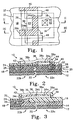
- FIGs. 1 to 3 A flash electrically erasable programmable read-only memory (EEPROM) unit cell 10 and portions of adjacent cells of an EEPROM array embodying the present invention are illustrated in FIGs. 1 to 3.
- the cell 10 is formed in a substrate 12 of N- conductivity type.
- a lightly doped well 14 of P- conductivity type is formed in the substrate 12.
- Field oxide insulators 16 insulate the cell 10 from the adjacent cells. It is further within the scope of the invention to provide the substrate 12 of P- conductivity type, in which case the well 14 is unnecessary.
- the cell 10 includes a source 18 and a drain 20 which are formed in the well 14, and a channel 22 which is defined in the well 14 between the source 18 and drain 20.
- the source 18 includes an N+ ohmic contact strata 24, and an underlying lightly doped N- strata 26 for reducing the electric field in the source depletion region and enabling a higher voltage to be applied to the source 18 for erasing the cell 10.
- the drain 20 includes an N+ ohmic contact strata 28, and an underlying shield strata 30 which is doped P, the opposite conductivity type to the strata 28, for increasing the hot electron injection efficiency between the N+ strata 28 and the shield strata 30.
- a tunnel oxide layer 32 having a thickness of typically 90-100 angstroms, is formed over the substrate 12.
- a polysilicon floating gate 34 is formed over the layer 32 and includes a program section 34a and an erase section 34b.
- the program section 34a overlies the channel programming region 22a, similar to normal flash EEPROM operation.
- a gap region 22b of the channel 22 is defined between the region 22a and the source 18 for controlling the erase threshold voltage.
- the erase section 34b of the floating gate 34 extends around the lower end (as viewed in FIG. 1) of the channel 22, over the field oxide insulator 16 and overlaps the source 18. As illustrated in FIG. 3, the erase section 34b has an end portion 34c which overlies portions of the tunnel oxide layer 32 and the source 18.
- a gate oxide layer 36 which typically has a thickness of 550 angstroms, is formed over the gap region 22b and the channel 22 in the source region.
- a layer 36a consisting of three sublayers of oxide/nitride/oxide (ONO), is formed over the floating gate 34 for control gate and floating gate isolation.
- a polysilicon control gate 38 is formed over the gate oxide layer 36 and the ONO layer 36a.
- a metal drain contact 40 extends through a hole in the oxide layers composed of tunnel oxide 32 and boro-phosphorosilicate glass (BSPG) which is not shown in the drawings. Further illustrated in FIGs. 2 and 3 are oxide sidewall spacers 42 and 44 which facilitate the fabrication of the cell 10.
- the polysilicon control gate 38 has a "split-gate" configuration, including a first section 38a which overlies the floating gate 34 and the programming region 22a of the channel 22.
- a second section 38b overlies the gap region 22b of the channel 22 and is disposed in series between the program section 34a of the floating gate 34 and the source 18.
- the second section 38b acts as a series enhancement mode gate which prevents the cell 10 from functioning as a depletion mode transistor if the floating gate 34 becomes over-erased.
- floating gate 34, control gate 38 are described and illustrated as being the same size and aligned with each other, they may differ in size and/or be offset from each other to an extent which depends on a particular application within the scope of the invention.
- the cell 10 is programmed by applying, typically, 12V to the control gate 38, 5-6V to the drain 20 and grounding the source 18.
- a high electric field is created in the drain depletion region between the drain 20 and the floating gate 34 by the applied voltages which causes impact ionization to occur in this region.
- Hole-electron pairs are created by the impact of the drain current in the high field region (they hit the silicon atoms). Some of the electrons generated by impact ionization are called "hot electrons".
- the control gate voltage causes hot electrons to be injected from the drain depletion region into the floating gate 34 through the program section 34a. These electrons are trapped in the floating gate 34 and create a negative charge therein which increases the threshold voltage of the cell 10.
- the cell 10 is read by applying 5V to the control gate 38 and 1-2V to the drain 20, and sensing the impedance of the cell 10 at the source 18. If the cell 10 is programmed and the threshold voltage (>6V) is higher than the control gate voltage (5V), the control gate voltage will be insufficient to enhance the channel 22 and the cell 10 will appear as a high impedance. If the cell 10 is not programmed or erased, the threshold voltage will be low, the control gate voltage will enhance the channel 22 and the cell 10 will appear as a low impedance.
- the cell 10 is erased by applying typically 12V to the source 18, grounding the control gate 38 and allowing the drain 20 to float. This causes the electrons which were injected into the floating gate 34 during programming to be removed by Fowler-Nordheim tunneling from the floating gate 34 through the thin tunnel oxide layer 32 to the source 18. Due to the split-gate configuration of the control gate 38, the gap region 22b of the channel 22 which underlies the series section 38b of the control gate 38 can be turned off by a normal control gate voltage, thereby providing the cell 10 with a stable threshold voltage after erasure and minimizing leakage.
- erasure is accomplished by Fowler-Nordheim tunneling from the end portion 34c of the erase section 34b of the floating gate 34 through the underlying tunnel oxide layer 32 to the source 18. Erasure can be accomplished with low applied voltages since the tunneling is only required to be performed through the thin oxide layer 32.
- the conventional split-gate EEPROM configuration requires tunneling for erasure to be performed through the portion of the thick gate oxide layer 36 which overlies the gap region 22b of the channel 22.
- a much higher potential difference is required to produce Fowler-Nordheim tunneling through the 550 angstrom oxide layer 36 than through the 90 angstrom oxide layer 32.
- the present cell 10 provides the threshold voltage control and over-erasure compensation of a split-gate EEPROM with the low voltage erasure of a basic EEPROM.
- FIG. 4 is similar to FIG. 1, but illustrates the control gate 38 highlighted by diagonal hatching.
- the control gate 38 constitutes a portion of a continuous "word line" 46 which interconnects the control gate 38 of the cell 10 with the control gates of the other cells in the vertical direction as viewed in FIGs. 1 and 4 to 7.
- FIG. 5 highlights an opening 48 which is cut in the floating polysilicon layer which forms the floating gate 34 to isolate the floating gate 34 from the floating gates of adjacent cells in the vertical direction.
- the opening 48 is filled with thick oxide during the formation of the gate oxide layer 36.
- FIG. 6 highlights the gate oxide layer 36 which fills the opening 48 and overlies the gap region 22b and the channel 22 at the source region.
- FIG. 7 highlights the insulator 16.
- FIG. 8 illustrates an EEPROM array 50 formed of unit cells 10 as illustrated in FIGs. 1 to 7.
- the array 50 is shown as including two columns of unit cells, although it can be expanded to any size within the scope of the invention.
- the array 50 includes an elongated common source region 52 which is formed in the substrate 12 and extends in a predetermined direction (vertical as viewed in the drawing).
- a first drain region 54a and a second drain 54b extend parallel to the source region 52 on opposite sides thereof.
- a first channel region 56a and a second channel region 56b are formed between the source region 52 and the drain regions 54a and 54b respectively.
- a plurality of first unit cells 10a and a plurality of second unit cells 10b are formed on the substrate 12 on the left and right sides of the source region 52 respectively and are vertically spaced from each other.
- the cells 10b are identical to the cells 10 described with reference to FIGs. 1 to 7.
- the cells 10a are identical to the cells 10b except that erase sections 34b' of floating gates 34' thereof extend rightwardly, rather than leftwardly as in the cells 10b, from program sections 34a' respectively toward the source region 52.
- the cells 10a and 10b include all of the elements of the cell 10. However, only the floating gates 34,34', field oxide insulators 16 and drain contacts 40 are shown for simplicity of illustration.
- the control gates 38 of the cells 10a and 10b are interconnected by word lines as indicated by broken lines 46a and 46b.
- the drain contacts 40 of cells 10a and 10b which are adjacent to each other in the horizontal direction are interconnected by "bit lines" indicated by broken lines 58a, 58b, 58c and 58d respectively.
- the erase sections 34b' of the cells 10a are vertically staggered from the erase sections 34b of the cells 10b.
- the ends of the erase sections 34b' and 34b overlap horizontally by a distance ⁇ . This arrangement enables the cells 10a and 10b to overlap each other horizontally, and reduce the size of the array 50.
- the flash EEPROM cell as described and illustrated has an N-type channel and the hot charge carriers which are injected into the floating gate are electrons, it is within the scope of the invention to provide a p-channel cell in which the injected hot charge carriers are holes.
Abstract
Description
- The present invention generally relates to the art of semiconductor memories, and more specifically to a flash or block erase electrically erasable programmable read-only memory (EEPROM) cell and array which are controllably erasable with low applied voltages.
- A flash or block erase EEPROM semiconductor memory includes an array of cells which can be independently programmed and read. The size of each cell and thereby the memory are made small by omitting select transistors which would enable the cells to be erased independently. All of the cells are erased together as a block.
- A conventional flash EEPROM is described in an article entitled "A FLASH-ERASE EEPROM CELL WITH AN ASYMMETRIC SOURCE AND DRAIN STRUCTURE", by H. Kume et al, IEDM, 25.8, 1987, pp. 560-563. Each cell includes a source and a drain which are formed on opposite sides of a channel region in a substrate. A thin tunnel oxide layer, a floating gate, a thick gate oxide layer and a control gate are formed over the channel region.
- The cell is programmed by applying, typically, 12V to the control gate, 6V to the drain and grounding the source, which causes hot electrons to be injected from the drain depletion region into the floating gate. Upon removal of the programming voltages, the injected electrons are trapped in the floating gate and create a negative charge therein which increases the threshold voltage of the cell to a value in excess of approximately 6V.
- The cell is read by applying 5V to the control gate and 1V to the drain, and sensing the impedance of the cell at the source. If the cell is programmed and the threshold voltage (6V) is higher than the control gate voltage (5V), the control gate voltage will be insufficient to enhance the channel and the cell will appear as a high impedance. If the cell is not programmed or erased, the threshold voltage will be low, the control gate voltage will enhance the channel and the cell will appear as a low impedance.
- The cell is erased by applying typically 12V to the source, grounding the control gate and allowing the drain to float. This causes the electrons which were injected into the floating gate during programming to be removed by Fowler-Nordheim tunneling from the floating gate through the thin tunnel oxide layer to the source.
- A problem with the conventional flash EEPROM cell configuration is that due to manufacturing tolerances, some cells become over-erased before other cells become erased sufficiently. The floating gates of the over-erased cells are depleted of electrons and become positively charged. This causes the over-erased cells to function as depletion mode transistors which cannot be turned off by normal operating voltages applied to their control gates, and introduces leakage during subsequent program and read operations.
- A known method of preventing over-erasure is to provide an adaptive erasing algorithm in which the erasing voltages are applied to the control gates as a series of pulses of varying period. This method is complicated and requires additional circuitry for generating the erase pulses in accordance with the algorithm.
- The effects of over-erasure can be compensated for by means of a split-gate (also known as stacked- or pass-gate) configuration in which a section of the control gate is disposed in series between the source and the floating gate. The region of the channel which underlies the series section of the control gate can be turned off by the control gate voltage, thereby providing the cell with a stable threshold voltage after erasure and minimizing leakage. A typical split-gate EEPROM is described in an article entitled "A 128K Flash EEPROM Using Double-Polysilicon Technology", by G. Samacisa et al, IEEE J. Solid-State Circuits, Vol. SC-22, No. 5, Oct. 1987, pp. 676-683.
- Although achieving stable erasure without the necessity of utilizing an adaptive algorithm, a split-gate EEPROM requires higher applied voltages to achieve erasure than the basic EEPROM. This is because the floating gate is spaced from the source by the series section of the control gate and the intervening gate oxide layer. A higher potential difference is required to accomplish erasure by Fowler-Nordheim tunneling through the thick gate oxide layer of the split-gate EEPROM than through the thin tunnel oxide layer of the basic EEPROM.
- A flash EEPROM cell embodying the present invention achieves the controlled erasure of the split-gate configuration with the low applied voltages of the basic design.
- More specifically, a flash EEPROM unit cell of the invention includes a control gate having a section thereof disposed in series between a program section of a floating gate and a source to provide threshold voltage control for erasure. The floating gate further has an erase section which extends from the program section around an end of a channel to the source. A thin tunnel oxide layer is formed between an end portion of the erase section and an underlying portion of the source which enables the floating gate to be erased by Fowler-Nordheim tunneling from the end portion through the oxide layer to the source with low applied voltages.
- An array of the present EEPROM cells includes a common elongated source region and a plurality of first and second unit cells which are spaced from each other along and on opposite sides of the source region respectively. The erase sections of the floating gates of the first cells are staggered from those of the second cells parallel to the source region, and may further overlap each other perpendicular to the source region to reduce the array size.
- These and other features and advantages of the present invention will be apparent to those skilled in the art from the following detailed description, taken together with the accompanying drawings, in which like reference numerals refer to like parts.
-
- FIG. 1 is a diagram illustrating an EEPROM unit cell embodying the present invention with a floating gate thereof highlighted by diagonal hatching;
- FIG. 2 is a section taken on a line II-II of FIG. 1;
- FIG. 3 is a section taken on a line III-III of FIG. 1;
- FIG. 4 is similar to FIG. 1 but has the polysilicon control gate (word line) highlighted by diagonal hatching;
- FIG. 5 is also similar to FIG. 1 but has floating polysilicon openings highlighted by diagonal hatching;
- FIG. 6 is also similar to FIG. 1 but has a gate oxide region highlighted by diagonal hatching;
- FIG. 7 is also similar to FIG. 1 but has field oxide regions highlighted by diagonal hatching; and
- FIG. 8 is a diagram illustrating an EEPROM array embodying the invention which is formed of unit cells as illustrated in FIGs. 1 to 7.
- A flash electrically erasable programmable read-only memory (EEPROM)
unit cell 10 and portions of adjacent cells of an EEPROM array embodying the present invention are illustrated in FIGs. 1 to 3. Thecell 10 is formed in asubstrate 12 of N- conductivity type. A lightly doped well 14 of P- conductivity type is formed in thesubstrate 12.Field oxide insulators 16 insulate thecell 10 from the adjacent cells. It is further within the scope of the invention to provide thesubstrate 12 of P- conductivity type, in which case thewell 14 is unnecessary. - The
cell 10 includes asource 18 and adrain 20 which are formed in thewell 14, and achannel 22 which is defined in thewell 14 between thesource 18 anddrain 20. As best viewed in FIG. 2, thesource 18 includes an N+ohmic contact strata 24, and an underlying lightly doped N-strata 26 for reducing the electric field in the source depletion region and enabling a higher voltage to be applied to thesource 18 for erasing thecell 10. - The
drain 20 includes an N+ohmic contact strata 28, and anunderlying shield strata 30 which is doped P, the opposite conductivity type to thestrata 28, for increasing the hot electron injection efficiency between theN+ strata 28 and theshield strata 30. - A
tunnel oxide layer 32, having a thickness of typically 90-100 angstroms, is formed over thesubstrate 12. Apolysilicon floating gate 34 is formed over thelayer 32 and includes aprogram section 34a and anerase section 34b. Theprogram section 34a overlies thechannel programming region 22a, similar to normal flash EEPROM operation. Agap region 22b of thechannel 22 is defined between theregion 22a and thesource 18 for controlling the erase threshold voltage. - As best viewed in FIGs. 1 and 3, the
erase section 34b of thefloating gate 34 extends around the lower end (as viewed in FIG. 1) of thechannel 22, over thefield oxide insulator 16 and overlaps thesource 18. As illustrated in FIG. 3, theerase section 34b has anend portion 34c which overlies portions of thetunnel oxide layer 32 and thesource 18. - A
gate oxide layer 36, which typically has a thickness of 550 angstroms, is formed over thegap region 22b and thechannel 22 in the source region. Alayer 36a, consisting of three sublayers of oxide/nitride/oxide (ONO), is formed over thefloating gate 34 for control gate and floating gate isolation. Apolysilicon control gate 38 is formed over thegate oxide layer 36 and theONO layer 36a. Ametal drain contact 40 extends through a hole in the oxide layers composed oftunnel oxide 32 and boro-phosphorosilicate glass (BSPG) which is not shown in the drawings. Further illustrated in FIGs. 2 and 3 areoxide sidewall spacers cell 10. - The
polysilicon control gate 38 has a "split-gate" configuration, including afirst section 38a which overlies the floatinggate 34 and theprogramming region 22a of thechannel 22. Asecond section 38b overlies thegap region 22b of thechannel 22 and is disposed in series between theprogram section 34a of the floatinggate 34 and thesource 18. Thesecond section 38b acts as a series enhancement mode gate which prevents thecell 10 from functioning as a depletion mode transistor if the floatinggate 34 becomes over-erased. - Although the corresponding sections of the
channel 22, floatinggate 34,control gate 38 are described and illustrated as being the same size and aligned with each other, they may differ in size and/or be offset from each other to an extent which depends on a particular application within the scope of the invention. - The
cell 10 is programmed by applying, typically, 12V to thecontrol gate 38, 5-6V to thedrain 20 and grounding thesource 18. A high electric field is created in the drain depletion region between thedrain 20 and the floatinggate 34 by the applied voltages which causes impact ionization to occur in this region. Hole-electron pairs are created by the impact of the drain current in the high field region (they hit the silicon atoms). Some of the electrons generated by impact ionization are called "hot electrons". - The control gate voltage causes hot electrons to be injected from the drain depletion region into the floating
gate 34 through theprogram section 34a. These electrons are trapped in the floatinggate 34 and create a negative charge therein which increases the threshold voltage of thecell 10. - The
cell 10 is read by applying 5V to thecontrol gate 38 and 1-2V to thedrain 20, and sensing the impedance of thecell 10 at thesource 18. If thecell 10 is programmed and the threshold voltage (>6V) is higher than the control gate voltage (5V), the control gate voltage will be insufficient to enhance thechannel 22 and thecell 10 will appear as a high impedance. If thecell 10 is not programmed or erased, the threshold voltage will be low, the control gate voltage will enhance thechannel 22 and thecell 10 will appear as a low impedance. - The
cell 10 is erased by applying typically 12V to thesource 18, grounding thecontrol gate 38 and allowing thedrain 20 to float. This causes the electrons which were injected into the floatinggate 34 during programming to be removed by Fowler-Nordheim tunneling from the floatinggate 34 through the thintunnel oxide layer 32 to thesource 18. Due to the split-gate configuration of thecontrol gate 38, thegap region 22b of thechannel 22 which underlies theseries section 38b of thecontrol gate 38 can be turned off by a normal control gate voltage, thereby providing thecell 10 with a stable threshold voltage after erasure and minimizing leakage. - In accordance with the invention, erasure is accomplished by Fowler-Nordheim tunneling from the
end portion 34c of the erasesection 34b of the floatinggate 34 through the underlyingtunnel oxide layer 32 to thesource 18. Erasure can be accomplished with low applied voltages since the tunneling is only required to be performed through thethin oxide layer 32. - In comparison, the conventional split-gate EEPROM configuration requires tunneling for erasure to be performed through the portion of the thick
gate oxide layer 36 which overlies thegap region 22b of thechannel 22. A much higher potential difference is required to produce Fowler-Nordheim tunneling through the 550angstrom oxide layer 36 than through the 90angstrom oxide layer 32. In this manner, thepresent cell 10 provides the threshold voltage control and over-erasure compensation of a split-gate EEPROM with the low voltage erasure of a basic EEPROM. - FIG. 4 is similar to FIG. 1, but illustrates the
control gate 38 highlighted by diagonal hatching. Thecontrol gate 38 constitutes a portion of a continuous "word line" 46 which interconnects thecontrol gate 38 of thecell 10 with the control gates of the other cells in the vertical direction as viewed in FIGs. 1 and 4 to 7. - FIG. 5 highlights an
opening 48 which is cut in the floating polysilicon layer which forms the floatinggate 34 to isolate the floatinggate 34 from the floating gates of adjacent cells in the vertical direction. Theopening 48 is filled with thick oxide during the formation of thegate oxide layer 36. - FIG. 6 highlights the
gate oxide layer 36 which fills theopening 48 and overlies thegap region 22b and thechannel 22 at the source region. FIG. 7 highlights theinsulator 16. - FIG. 8 illustrates an
EEPROM array 50 formed ofunit cells 10 as illustrated in FIGs. 1 to 7. Thearray 50 is shown as including two columns of unit cells, although it can be expanded to any size within the scope of the invention. Thearray 50 includes an elongatedcommon source region 52 which is formed in thesubstrate 12 and extends in a predetermined direction (vertical as viewed in the drawing). Afirst drain region 54a and asecond drain 54b extend parallel to thesource region 52 on opposite sides thereof. Afirst channel region 56a and asecond channel region 56b are formed between thesource region 52 and thedrain regions - A plurality of
first unit cells 10a and a plurality ofsecond unit cells 10b are formed on thesubstrate 12 on the left and right sides of thesource region 52 respectively and are vertically spaced from each other. Thecells 10b are identical to thecells 10 described with reference to FIGs. 1 to 7. Thecells 10a are identical to thecells 10b except that erasesections 34b' of floatinggates 34' thereof extend rightwardly, rather than leftwardly as in thecells 10b, fromprogram sections 34a' respectively toward thesource region 52. - The
cells cell 10. However, only the floatinggates field oxide insulators 16 anddrain contacts 40 are shown for simplicity of illustration. Thecontrol gates 38 of thecells broken lines drain contacts 40 ofcells broken lines - In accordance with the invention, the erase
sections 34b' of thecells 10a are vertically staggered from the erasesections 34b of thecells 10b. In addition, the ends of the erasesections 34b' and 34b overlap horizontally by a distance Δ. This arrangement enables thecells array 50. - While several illustrative embodiments of the invention have been shown and described, numerous variations and alternate embodiments will occur to those skilled in the art, without departing from the spirit and scope of the invention.
- For example, although the flash EEPROM cell as described and illustrated has an N-type channel and the hot charge carriers which are injected into the floating gate are electrons, it is within the scope of the invention to provide a p-channel cell in which the injected hot charge carriers are holes.
- Accordingly, it is intended that the present invention not be limited solely to the specifically described illustrative embodiments. Various modifications are contemplated and can be made without departing from the spirit and scope of the invention as defined by the appended claims.
Claims (10)
- An electrically erasable programmable read-only memory (EEPROM) cell, comprising:
a semiconductor substrate;
a source and a drain formed in the substrate;
a channel which is formed in the substrate and has a programming region extending from the drain toward the source and a gap region between the source and said programming region;
a tunnel insulating layer formed over the substrate;
a floating gate which is formed over the tunnel insulating layer and includes:
a program section overlying said programming region of the channel; and
an erase section which extends from said program section and overlaps the source;
a gate insulating layer formed over said program section of the floating gate and said gap region of the channel; and
a control gate which is formed over the gate insulating layer and overlies said program and erase sections of the floating gate and said gap region of the channel. - A cell as in claim 1, in which said erase section of the floating gate extends from said program section thereof around the channel to the source.
- A cell as in claim 1, in which said erase section of the floating gate extends from an end of said program section thereof around an end of the channel to the source.
- A cell as in claim 3, further comprising a field insulator formed in the substrate adjacent to said end of the channel, said erase section of the floating gate extending over said field insulator.
- A cell as in claim 1, in which the gate insulating layer is thicker than the tunnel insulating layer.
- A cell as in claim 1, in which the tunnel and gate insulating layers are formed of oxide.
- An electrically erasable programmable read-only memory (EEPROM) array, comprising:
a semiconductor substrate;
an elongated source region which is formed in the substrate and extends in a predetermined direction; and
a plurality of first cells which are formed on the substrate extending from one side of said source region and are spaced from each other in said predetermined direction; and
a plurality of second cells which are formed on the substrate extending from an opposite side of said source region and are spaced from each other in said predetermined direction;
each first and second cell including:
a source which constitutes a portion of said source region;
a drain formed in the substrate;
a channel which is formed in the substrate and has a programming region extending from the drain toward the source and a gap region between the source and said programming region;
a tunnel insulating layer formed over the substrate;
a floating gate which is formed over the tunnel insulating layer and includes:
a program section overlying said programming region of the channel; and
an erase section which extends from said program section and overlaps the source;
a gate insulating layer formed over said program section of the floating gate and said gap region of the channel; and
a control gate which is formed over the gate insulating layer and overlies said program and erase sections of the floating gate and said gap region of the channel; in which
said erase sections of the control gates of the first cells are staggered from said erase sections of the control gates of the second cells in said predetermined direction. - An array as in claim 7, in which said erase sections of the control gates of the first cells overlap said erase sections of the control gates of the second cells perpendicular to said predetermined direction.
- An array as in claim 7, in which:
said erase section of the floating gate of each first and second cell extends from an end of said program section around an end of the channel to the respective source. - An array as in claim 7, in which the gate insulating layer is thicker than the tunnel insulating layer.
Applications Claiming Priority (2)
| Application Number | Priority Date | Filing Date | Title |
|---|---|---|---|
| US47134 | 1993-04-16 | ||
| US08/047,134 US5343424A (en) | 1993-04-16 | 1993-04-16 | Split-gate flash EEPROM cell and array with low voltage erasure |
Publications (2)
| Publication Number | Publication Date |
|---|---|
| EP0620600A2 true EP0620600A2 (en) | 1994-10-19 |
| EP0620600A3 EP0620600A3 (en) | 1995-01-18 |
Family
ID=21947246
Family Applications (1)
| Application Number | Title | Priority Date | Filing Date |
|---|---|---|---|
| EP94302670A Withdrawn EP0620600A3 (en) | 1993-04-16 | 1994-04-14 | Split-gate flash EEPROM cell and array with low voltage erasure. |
Country Status (4)
| Country | Link |
|---|---|
| US (1) | US5343424A (en) |
| EP (1) | EP0620600A3 (en) |
| JP (1) | JPH0750350A (en) |
| TW (1) | TW246745B (en) |
Families Citing this family (5)
| Publication number | Priority date | Publication date | Assignee | Title |
|---|---|---|---|---|
| US5397726A (en) * | 1992-02-04 | 1995-03-14 | National Semiconductor Corporation | Segment-erasable flash EPROM |
| US5528651A (en) * | 1994-06-09 | 1996-06-18 | Elekta Instrument Ab | Positioning device and method for radiation treatment |
| US5511036A (en) * | 1994-12-19 | 1996-04-23 | Hughes Aircraft Company | Flash EEPROM cell and array with bifurcated floating gates |
| US5844271A (en) * | 1995-08-21 | 1998-12-01 | Cypress Semiconductor Corp. | Single layer polycrystalline silicon split-gate EEPROM cell having a buried control gate |
| US6125060A (en) * | 1998-05-05 | 2000-09-26 | Chang; Ming-Bing | Flash EEPROM device employing polysilicon sidewall spacer as an erase gate |
Citations (5)
| Publication number | Priority date | Publication date | Assignee | Title |
|---|---|---|---|---|
| US4317272A (en) * | 1979-10-26 | 1982-03-02 | Texas Instruments Incorporated | High density, electrically erasable, floating gate memory cell |
| EP0247875A2 (en) * | 1986-05-30 | 1987-12-02 | Seeq Technology, Incorporated | Block electrically erasable eeprom |
| EP0360504A2 (en) * | 1988-09-22 | 1990-03-28 | Advanced Micro Devices Inc. | One transistor flash eprom cell |
| US4998220A (en) * | 1988-05-03 | 1991-03-05 | Waferscale Integration, Inc. | EEPROM with improved erase structure |
| US5130769A (en) * | 1991-05-16 | 1992-07-14 | Motorola, Inc. | Nonvolatile memory cell |
Family Cites Families (3)
| Publication number | Priority date | Publication date | Assignee | Title |
|---|---|---|---|---|
| US5168465A (en) * | 1988-06-08 | 1992-12-01 | Eliyahou Harari | Highly compact EPROM and flash EEPROM devices |
| US5057886A (en) * | 1988-12-21 | 1991-10-15 | Texas Instruments Incorporated | Non-volatile memory with improved coupling between gates |
| JPH03245575A (en) * | 1990-02-22 | 1991-11-01 | Mitsubishi Electric Corp | Semiconductor memory device and manufacture thereof |
-
1993
- 1993-04-16 US US08/047,134 patent/US5343424A/en not_active Expired - Fee Related
-
1994
- 1994-04-14 EP EP94302670A patent/EP0620600A3/en not_active Withdrawn
- 1994-04-14 TW TW083103336A patent/TW246745B/zh active
- 1994-04-15 JP JP6077635A patent/JPH0750350A/en active Pending
Patent Citations (5)
| Publication number | Priority date | Publication date | Assignee | Title |
|---|---|---|---|---|
| US4317272A (en) * | 1979-10-26 | 1982-03-02 | Texas Instruments Incorporated | High density, electrically erasable, floating gate memory cell |
| EP0247875A2 (en) * | 1986-05-30 | 1987-12-02 | Seeq Technology, Incorporated | Block electrically erasable eeprom |
| US4998220A (en) * | 1988-05-03 | 1991-03-05 | Waferscale Integration, Inc. | EEPROM with improved erase structure |
| EP0360504A2 (en) * | 1988-09-22 | 1990-03-28 | Advanced Micro Devices Inc. | One transistor flash eprom cell |
| US5130769A (en) * | 1991-05-16 | 1992-07-14 | Motorola, Inc. | Nonvolatile memory cell |
Also Published As
| Publication number | Publication date |
|---|---|
| EP0620600A3 (en) | 1995-01-18 |
| TW246745B (en) | 1995-05-01 |
| US5343424A (en) | 1994-08-30 |
| JPH0750350A (en) | 1995-02-21 |
Similar Documents
| Publication | Publication Date | Title |
|---|---|---|
| US5812449A (en) | Flash EEPROM cell, method of manufacturing the same, method of programming and method of reading the same | |
| EP0360504B1 (en) | One transistor flash eprom cell | |
| US5824584A (en) | Method of making and accessing split gate memory device | |
| US5379253A (en) | High density EEPROM cell array with novel programming scheme and method of manufacture | |
| US7060563B2 (en) | Local SONOS-type structure having two-piece gate and self-aligned ONO and method for manufacturing the same | |
| US5378909A (en) | Flash EEPROM cell having gap between floating gate and drain for high hot electron injection efficiency for programming | |
| KR0172016B1 (en) | Non-volatile semiconductor memory having programming region for injecting & ejecting carrier into and from floating gate | |
| US5760435A (en) | Use of spacers as floating gates in EEPROM with doubled storage efficiency | |
| US6828618B2 (en) | Split-gate thin-film storage NVM cell | |
| US5455791A (en) | Method for erasing data in EEPROM devices on SOI substrates and device therefor | |
| US5612914A (en) | Asymmetrical non-volatile memory cell, arrays and methods for fabricating same | |
| JP2848223B2 (en) | Erasing method and manufacturing method for nonvolatile semiconductor memory device | |
| US20040105313A1 (en) | Erasing method for p-channel NROM | |
| US6580135B2 (en) | Silicon nitride read only memory structure and method of programming and erasure | |
| JP2758577B2 (en) | EEPROM and its manufacturing method | |
| KR20010072087A (en) | Electrically erasable nonvolatile memory | |
| US5814857A (en) | EEPROM flash memory cell, memory device, and process for formation thereof | |
| KR100558004B1 (en) | Programing method of a non-volatile memory device including a charge storage layer between a gate electrode and a semiconductor substrate | |
| KR19980035933A (en) | Nonvolatile memory device | |
| US4577295A (en) | Hybrid E2 cell and related array | |
| KR100298586B1 (en) | Non-Volatile Memory device | |
| US5343424A (en) | Split-gate flash EEPROM cell and array with low voltage erasure | |
| JP4969748B2 (en) | Nonvolatile semiconductor memory device and method of manufacturing nonvolatile memory cell | |
| US5511036A (en) | Flash EEPROM cell and array with bifurcated floating gates | |
| US6963508B1 (en) | Operation method for non-volatile memory |
Legal Events
| Date | Code | Title | Description |
|---|---|---|---|
| PUAI | Public reference made under article 153(3) epc to a published international application that has entered the european phase |
Free format text: ORIGINAL CODE: 0009012 |
|
| AK | Designated contracting states |
Kind code of ref document: A2 Designated state(s): DE FR GB |
|
| PUAL | Search report despatched |
Free format text: ORIGINAL CODE: 0009013 |
|
| AK | Designated contracting states |
Kind code of ref document: A3 Designated state(s): DE FR GB |
|
| 17P | Request for examination filed |
Effective date: 19950626 |
|
| 17Q | First examination report despatched |
Effective date: 19970114 |
|
| STAA | Information on the status of an ep patent application or granted ep patent |
Free format text: STATUS: THE APPLICATION IS DEEMED TO BE WITHDRAWN |
|
| 18D | Application deemed to be withdrawn |
Effective date: 19970527 |