EP0620640A1 - Piezoelectric filter - Google Patents
Piezoelectric filter Download PDFInfo
- Publication number
- EP0620640A1 EP0620640A1 EP94105729A EP94105729A EP0620640A1 EP 0620640 A1 EP0620640 A1 EP 0620640A1 EP 94105729 A EP94105729 A EP 94105729A EP 94105729 A EP94105729 A EP 94105729A EP 0620640 A1 EP0620640 A1 EP 0620640A1
- Authority
- EP
- European Patent Office
- Prior art keywords
- substrate
- filter
- electrodes
- piezoelectric
- major surface
- Prior art date
- Legal status (The legal status is an assumption and is not a legal conclusion. Google has not performed a legal analysis and makes no representation as to the accuracy of the status listed.)
- Granted
Links
Images


Classifications
-
- H—ELECTRICITY
- H03—ELECTRONIC CIRCUITRY
- H03H—IMPEDANCE NETWORKS, e.g. RESONANT CIRCUITS; RESONATORS
- H03H9/00—Networks comprising electromechanical or electro-acoustic devices; Electromechanical resonators
- H03H9/02—Details
- H03H9/02007—Details of bulk acoustic wave devices
- H03H9/02015—Characteristics of piezoelectric layers, e.g. cutting angles
- H03H9/02031—Characteristics of piezoelectric layers, e.g. cutting angles consisting of ceramic
-
- H—ELECTRICITY
- H03—ELECTRONIC CIRCUITRY
- H03H—IMPEDANCE NETWORKS, e.g. RESONANT CIRCUITS; RESONATORS
- H03H9/00—Networks comprising electromechanical or electro-acoustic devices; Electromechanical resonators
- H03H9/46—Filters
- H03H9/54—Filters comprising resonators of piezo-electric or electrostrictive material
- H03H9/56—Monolithic crystal filters
- H03H9/562—Monolithic crystal filters comprising a ceramic piezoelectric layer
Definitions
- the present invention relates to a multi-mode piezoelectric filter.
- a filter used in a MHz frequency range having a wide bandwidth of the passband and high temperature stability of frequency has been required in the market of a communication device or the like.
- a multi-mode filter is generally employed in the MHz frequency range since it is able to reduce spurious response and is easy to be manufactured.
- this filter is made of material such as piezoelectric ceramics or quartz crystal.
- a multi-mode filter made of quartz crystal has excellent temperature stability.
- an object of the present invention is to provide a multi-mode piezoelectric filter having high temperature stability and having a wide bandwidth in the MHz frequency range.
- Another object of the present invention is to provide a multi-mode piezoelectric filter which can reduce spurious response and improve group delay characteristics.
- a piezoelectric filter according to the present invention comprises a thin piezoelectric substrate made of a LiTaO3 single crystal.
- a pair of spaced electrodes are formed adjacently on a front major surface of the substrate, and a counter electrode is formed on a rear major surface of the substrate in opposition to the spaced electrodes.
- the spaced electrodes and the counter electrode coact with a portion of said substrate located therebetween to establish an energy trapped type multi-mode filter element vibrating in the thickness shear mode.
- Two or more pairs of spaced electrodes may preferably be formed on the front major surface of the substrate, and a counter electrode may preferably be formed on the rear major surface of the substrate in opposition to the spaced electrodes.
- the spaced electrodes and the counter electrode coact with portions of the substrate located therebetween to form two or more energy trapped type multi-mode filter elements vibrating in the thickness shear mode such that the filter elements are coupled to form a cascade connection.
- An X-cut of the LiTaO3 single crystal is easy to be cut due to a cleavage plane which is provided at - 57° from the Y-axis. Further, the LiTaO3 is preferably cut from an X-cut at an angle of - 57° ⁇ 0.5° from the Y-axis since its temperature characteristics, roll-off characteristics and group delay characteristics are all satisfactory.
- the LiTaO3 single crystal Since the LiTaO3 single crystal has a small d-constant, a vibration excited therein is sensitively influenced by damping.
- silicone rubber well-known damping material
- the response of principal vibration of the LiTaO3 single crystal is so excessively suppressed that the loss is increased.
- the characteristic of silicone rubber such as hardness is considerably varied by temperature changes, the loss is largely varied due to temperature changes. Therefore, silicone gel is used as damping material in a preferred embodiment of the present invention. Since silicone gel is softer than silicone rubber and its temperature coefficient is smaller than that of silicone rubber, the loss is reduced due to a little damping effect and the temperature stability of the loss is improved.
- Figs. 1 and 2 show a piezoelectric filter formed as a chip component according to an embodiment of the present invention.
- This filter comprises a filter unit 1, a case 20 storing the unit 1, and a cover 30 which is bonded to the case 20 to close its opening.
- the unit 1 comprises an elongated rectangular thin piezoelectric substrate 2 having front and rear major surfaces.
- the substrate 2 is made of an X-cut of a LiTaO3 single crystal which is cut at an angle of - 57 ° ⁇ 0.5° from the Y-axis, as shown in Fig. 4.
- Input and output terminal electrodes 3 and 4 are formed on both ends of the front major surface of the substrate 2, while a ground terminal electrode 11 is formed on a center of the rear major surface of the substrate 2.
- Two pairs of spaced electrodes 5, 7 and 6, 8 are formed on the front major surface of the substrate 2, and counter electrodes 9 and 10 are formed on the rear major surface of the substrate 2 in opposition to the spaced electrodes 5, 7 and 6, 8 respectively.
- the terminal electrodes 3 and 4 are connected with the electrodes 5 and 6 through extracting electrodes 12 and 13 respectively.
- the electrodes 5 and 6 are connected together by an extracting electrode 14.
- the counter electrodes 9 and 10 are connected through extracting electrodes 15 and 16 and the terminal electrode 11.
- the electrodes 3 - 11 are all extended in the widthwise direction parallel to the shorter edges of the substrate 2.
- the electrodes 5, 7 and the counter electrode 9 coact with the intervening portion of the substrate 2 to form a first energy trapped type multi-mode filter element F1
- the electrodes 6, 8 and the counter electrode 10 coact with the intervening portion of the substrate 2 to form a second energy trapped type multi-mode filter element F2 such that the two elements F1 and F2 are coupled to form a cascade connection.
- These elements F1 and F2 vibrate in a thickness shear mode.
- the case 20 which is made of insulating material such as alumina ceramics or resin, is provided on its upper surface with a cavity 21 for storing the unit 1.
- External electrodes 22 and 23 are formed on inner surfaces of both end portions of the cavity 21 to extend toward outer surfaces of both end portions of the case 20.
- External electrode 24 is formed on inner surfaces of a central portion of the cavity 21 to extend toward outer surfaces of a central portion of the case 20.
- Concave portions 25 and 26 which serve as vibration spaces are formed on a bottom of the cavity 21 between the external electrodes 22, 23 and 24.
- the unit 1 is stored in the cavity 21 of the case 20, and fixed thereto with conductive adhesive or solder (not shown). At the same time, the terminal electrodes 3, 4 and 11 of the unit 1 are connected with the external electrodes 22, 23 and 24 of the case 20 respectively.
- the cover 30, which is made of insulating material similar to the case 20, is provided on its outer surface with three external electrodes 31, 32 and 33. These electrodes 31, 32 and 33 are connected with the external electrodes 22, 23 and 24 respectively.
- Silicone gel 27 is applied in the cavity 21 so as to coat at least the elements F1 and F2 of the unit 1, as shown in Fig. 2. At the same time, the concave portions 25 and 26 are filled up with this silicon gel 27.
- Fig. 5 is a circuit diagram of the aforementioned component.
- Table shows 3 dB bandwidth and frequency deviation level in a temperature range (- 20° C to 60 ° C) of multi-mode filters which are made of piezoelectric ceramics (PZT), quartz crystal and an X-cut (Y-57° ) of a LiTaO3 single crystal respectively.
- Type 3 dB bandwidth Frequency Deviation Piezoelectric Ceramics 0.3 ⁇ 3 % about ⁇ 0.2 % Quartz Crystal 0.02 ⁇ 0.2 % about ⁇ 0.01 %
- the X-cut of LiTaO3 has the largest 3 dB bandwidth, and has the frequency deviation in the middle of those of the piezoelectric ceramics and quartz crystal.
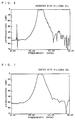
- Fig. 6 shows filter characteristics of the unit 1 uncoated with silicone gel 27
- Fig. 7 shows those of the unit 1 coated with the silicon gel 27.
- Fig. 8 shows a top waveform and group delay characteristics of the unit 1 uncoated with silicone gel 27, and Fig. 9 shows those of the unit 1 coated with silicone gel 27.
- Fig. 10 shows temperature dependence of loss of a filter unit employing silicone rubber having hardness of 15 JIS A (Japanese Industrial Standard A).
- Figs. 11 and 12 show temperature dependence of loss of filter units employing silicone gels having penetration of 50 and 150.
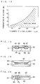
- Fig. 13 illustrates relation between the thickness of a filter unit which is made of an X-cut (Y - 57° ) of a LiTaO3 single crystal and penetration of silicone gel. Referring to Fig. 11, a practical range is shown with slant lines.
- the piezoelectric substrate is made of an X-cut of a LiTaO3 which is cut at an angle of - 57° ⁇ 0.5° from the Y-axis in the aforementioned embodiment, the present invention is not restricted to this. It is possible to attain substantially similar characteristics by employing an X-cut which is cut at another angle such as - 50° or - 58° from the Y-axis.
- electrode patterns of the multi-mode filter according to the present invention are not restricted to those shown in Fig. 3, but may be replaced by those shown in Figs. 14, 15 or 16.
- Fig. 14 illustrates two-element type filter unit according to a second embodiment of the present invention.
- numeral 40 denotes a substrate of an X-cut of a LiTaO3 single crystal
- numerals 41, 42 and 43 denote terminal electrodes
- numerals 44, 45 and 46, 47 denote spaced electrodes
- numerals 48 and 49 denote counter electrodes corresponding to the electrodes 44, 45 and 46, 47.
- the spaced electrodes 44, 45 and 46, 47, the counter electrodes 48 and 49 and the ground terminal electrode 43 are not extended in the widthwise direction of the substrate 40.
- Fig. 15 illustrates a different pattern of two-element type filter unit from Fig. 14 in that input and output terminal electrodes 50 and 51 are formed on the two corners of the substrate 40 and two ground terminal electrodes 52 and 53 are formed on the remaining two corners of the substrate 40.
- Fig. 16 illustrates one-element type filter unit according to a fourth embodiment of the present invention.
- numeral 60 denotes a substrate of an X-cut of a LiTaO3 single crystal
- numerals 61, 62 and 63 denote terminal electrodes
- numerals 64 and 65 denote spaced electrodes
- numeral 66 denotes counter electrode corresponding to the spaced electrodes 64 and 65.
- one energy trapped type multi-mode filter element F3 vibrating in the thickness shear mode is formed by the spaced electrodes 64 and 65 and the counter electrode 66 coacting with the intervening portion of the substrate 60.
- the present invention is not restricted to the filter having one or two multi-mode filter elements formed on a single substrate, but is also applicable to a filter having three or more multi-mode filter elements.
- the piezoelectric filter according to the present invention comprises a substrate made of a LiTaO3 single crystal and at least one energy trapped type multi-mode filter element vibrating in a thickness shear mode formed on the substrate, it is possible to obtain a filter having high temperature stability and having a bandwidth which is wider than those of filters made of piezoelectric ceramics and quartz crystal.
- damping material such as silicone gel onto the filter element, thereby improving the group delay characteristics and the roll-off characteristics.
Abstract
Description
- The present invention relates to a multi-mode piezoelectric filter.
- In recent years, a filter used in a MHz frequency range having a wide bandwidth of the passband and high temperature stability of frequency has been required in the market of a communication device or the like. A multi-mode filter is generally employed in the MHz frequency range since it is able to reduce spurious response and is easy to be manufactured. In general, this filter is made of material such as piezoelectric ceramics or quartz crystal.
- When a multi-mode filter is made of piezoelectric ceramics, however, it is difficult to obtain high temperature stability, since its frequency greatly varies in relation to temperature in a practical temperature range (- 20° C to 80 ° C).
- On the other hand, a multi-mode filter made of quartz crystal has excellent temperature stability. However, it is difficult for this filter to satisfy the requirement in the market of the communication device since its bandwidth is too narrow.
- Accordingly, an object of the present invention is to provide a multi-mode piezoelectric filter having high temperature stability and having a wide bandwidth in the MHz frequency range.
- Another object of the present invention is to provide a multi-mode piezoelectric filter which can reduce spurious response and improve group delay characteristics.
- In order to attain the aforementioned objects, a piezoelectric filter according to the present invention comprises a thin piezoelectric substrate made of a LiTaO₃ single crystal. A pair of spaced electrodes are formed adjacently on a front major surface of the substrate, and a counter electrode is formed on a rear major surface of the substrate in opposition to the spaced electrodes. The spaced electrodes and the counter electrode coact with a portion of said substrate located therebetween to establish an energy trapped type multi-mode filter element vibrating in the thickness shear mode.
- Two or more pairs of spaced electrodes may preferably be formed on the front major surface of the substrate, and a counter electrode may preferably be formed on the rear major surface of the substrate in opposition to the spaced electrodes. In this case, the spaced electrodes and the counter electrode coact with portions of the substrate located therebetween to form two or more energy trapped type multi-mode filter elements vibrating in the thickness shear mode such that the filter elements are coupled to form a cascade connection.
- The LiTaO₃ single crystal, which is one of piezoelectric single crystals, has small temperature coefficient of frequency as compared with piezoelectric ceramics, and a large electromechanical coupling factor as compared with quartz crystal, i.e. coupling factor k₁₅ = 46, temperature coefficient T c =2 ppm/° C in LiTaO₃ single crystal. Therefore, a filter made of the LiTaO₃ single crystal is superior in temperature characteristics to that made of piezoelectric ceramics, and wider in bandwidth than that made of quartz crystal.
- In the LiTaO₃ single crystal, unwanted vibration is easily excited so as to increase a spurious response. Therefore, a thickness shear vibration mode having a smaller spurious response than other vibration modes is used in the present invention.
- An X-cut of the LiTaO₃ single crystal is easy to be cut due to a cleavage plane which is provided at - 57° from the Y-axis. Further, the LiTaO₃ is preferably cut from an X-cut at an angle of - 57° ± 0.5° from the Y-axis since its temperature characteristics, roll-off characteristics and group delay characteristics are all satisfactory.
- The LiTaO₃ single crystal has a distorted top waveform since its Q-value is larger than that of piezoelectric ceramics (Q = 5000 in LiTaO₃ single crystal, Q = 1000 in PZT), and hence group delay deviation may disadvantageously be increased. Therefore, it is preferable to apply damping material at least on the filter element in order to effectively suppress the spurious response. Further, it is possible to reduce the Q-value, round the top waveform and reduce the group delay deviation by applying such damping material.
- Since the LiTaO₃ single crystal has a small d-constant, a vibration excited therein is sensitively influenced by damping. When silicone rubber, well-known damping material, is employed, the response of principal vibration of the LiTaO₃ single crystal is so excessively suppressed that the loss is increased. Further, since the characteristic of silicone rubber such as hardness is considerably varied by temperature changes, the loss is largely varied due to temperature changes. Therefore, silicone gel is used as damping material in a preferred embodiment of the present invention. Since silicone gel is softer than silicone rubber and its temperature coefficient is smaller than that of silicone rubber, the loss is reduced due to a little damping effect and the temperature stability of the loss is improved.
- The foregoing and other objects, features, aspects and advantages of the present invention will become more apparent from the following detailed description of the present invention when taken in conjunction with the accompanying drawings.
-
- Fig. 1 is a perspective view showing a piezoelectric filter component according to an embodiment of the present invention;
- Fig. 2 is a sectional view of the piezoelectric filter component shown in Fig. 1;
- Fig. 3 is a front elevational view showing a filter unit;
- Fig. 4 illustrates a cut angle of a piezoelectric substrate;
- Fig. 5 is a circuit diagram of the piezoelectric filter;
- Fig. 6 illustrates filter characteristics of the filter unit uncoated with silicone gel;
- Fig. 7 illustrates filter characteristics of the filter unit coated with silicone gel;
- Fig. 8 illustrates a top waveform and group delay characteristics of the filter unit uncoated with silicone gel;
- Fig. 9 illustrates a top waveform and group delay characteristics of the filter unit coated with silicone gel;
- Fig. 10 is a characteristic diagram showing a relation between temperature and loss in a filter coated with silicone rubber;
- Fig. 11 is a characteristic diagram showing a relation between temperature and loss in a filter coated with silicone gel;
- Fig. 12 is a characteristic diagram showing a relation between temperature and loss in a filter coated with another silicone gel;
- Fig. 13 illustrates relation between the thickness of a filter unit which is made of a LiTaO₃ single crystal and penetration of silicone gel;
- Fig. 14 is a front elevational view showing a filter unit according to a second embodiment of the present invention;
- Fig. 15 is a front elevational view showing a filter unit according to a third embodiment of the present invention; and
- Fig. 16 is a front elevational view showing a filter unit according to a fourth embodiment of the present invention.
- Figs. 1 and 2 show a piezoelectric filter formed as a chip component according to an embodiment of the present invention.
- This filter comprises a
filter unit 1, acase 20 storing theunit 1, and acover 30 which is bonded to thecase 20 to close its opening. - As shown in Fig. 3, the
unit 1 comprises an elongated rectangular thinpiezoelectric substrate 2 having front and rear major surfaces. Thesubstrate 2 is made of an X-cut of a LiTaO₃ single crystal which is cut at an angle of - 57 ° ± 0.5° from the Y-axis, as shown in Fig. 4. Input andoutput terminal electrodes substrate 2, while a ground terminal electrode 11 is formed on a center of the rear major surface of thesubstrate 2. Two pairs of spacedelectrodes substrate 2, andcounter electrodes substrate 2 in opposition to the spacedelectrodes terminal electrodes electrodes electrodes electrodes electrode 14. Thecounter electrodes electrodes 15 and 16 and the terminal electrode 11. The electrodes 3 - 11 are all extended in the widthwise direction parallel to the shorter edges of thesubstrate 2. - The
electrodes counter electrode 9 coact with the intervening portion of thesubstrate 2 to form a first energy trapped type multi-mode filter element F₁, and theelectrodes counter electrode 10 coact with the intervening portion of thesubstrate 2 to form a second energy trapped type multi-mode filter element F₂ such that the two elements F₁ and F₂ are coupled to form a cascade connection. These elements F₁ and F₂ vibrate in a thickness shear mode. - The
case 20, which is made of insulating material such as alumina ceramics or resin, is provided on its upper surface with acavity 21 for storing theunit 1.External electrodes cavity 21 to extend toward outer surfaces of both end portions of thecase 20.External electrode 24 is formed on inner surfaces of a central portion of thecavity 21 to extend toward outer surfaces of a central portion of thecase 20.Concave portions cavity 21 between theexternal electrodes unit 1 is stored in thecavity 21 of thecase 20, and fixed thereto with conductive adhesive or solder (not shown). At the same time, theterminal electrodes unit 1 are connected with theexternal electrodes case 20 respectively. - The
cover 30, which is made of insulating material similar to thecase 20, is provided on its outer surface with threeexternal electrodes electrodes external electrodes -
Silicone gel 27 is applied in thecavity 21 so as to coat at least the elements F₁ and F₂ of theunit 1, as shown in Fig. 2. At the same time, theconcave portions silicon gel 27. - Fig. 5 is a circuit diagram of the aforementioned component.
- The following Table shows 3 dB bandwidth and frequency deviation level in a temperature range (- 20° C to 60 ° C) of multi-mode filters which are made of piezoelectric ceramics (PZT), quartz crystal and an X-cut (Y-57° ) of a LiTaO₃ single crystal respectively.
Type 3 dB bandwidth Frequency Deviation Piezoelectric Ceramics 0.3∼3 % about ± 0.2 % Quartz Crystal 0.02∼0.2 % about ± 0.01 % X-Cut of LiTaO₃ 2 ∼ 4 % about ± 0.05 % - As the above Table clearly shows, the X-cut of LiTaO₃ has the largest 3 dB bandwidth, and has the frequency deviation in the middle of those of the piezoelectric ceramics and quartz crystal.
- Fig. 6 shows filter characteristics of the
unit 1 uncoated withsilicone gel 27, and Fig. 7 shows those of theunit 1 coated with thesilicon gel 27. These figures clearly show that a spurious response is effectively suppressed by applyingsilicone gel 27 while a principal response is less suppressed, so that the filter characteristics is highly improved. - Fig. 8 shows a top waveform and group delay characteristics of the
unit 1 uncoated withsilicone gel 27, and Fig. 9 shows those of theunit 1 coated withsilicone gel 27. These figures clearly show that the top waveform is rounded so as to improve the roll-off characteristics and the group delay deviation is reduced by applyingsilicone gel 27. - The comparison between characteristics of silicone rubber and those of silicone gel serving as damping material is now described.
- Fig. 10 shows temperature dependence of loss of a filter unit employing silicone rubber having hardness of 15 JIS A (Japanese Industrial Standard A).
- Figs. 11 and 12 show temperature dependence of loss of filter units employing silicone gels having penetration of 50 and 150.
- These figures show that the filter units employing silicone gel have smaller loss and smaller temperature dependence of the loss than that of the filter unit employing the silicon rubber. Also, the temperature dependence of loss decreases as the penetration of the silicon gels increases. On the other hand, group delay characteristics are deteriorated as the penetration of silicone gel increases.
- Fig. 13 illustrates relation between the thickness of a filter unit which is made of an X-cut (Y - 57° ) of a LiTaO₃ single crystal and penetration of silicone gel. Referring to Fig. 11, a practical range is shown with slant lines.
- As shown in Fig. 13, it is necessary to increase penetration of silicone gel as the thickness of the unit decreases.
- Though the piezoelectric substrate is made of an X-cut of a LiTaO₃ which is cut at an angle of - 57° ± 0.5° from the Y-axis in the aforementioned embodiment, the present invention is not restricted to this. It is possible to attain substantially similar characteristics by employing an X-cut which is cut at another angle such as - 50° or - 58° from the Y-axis.
- Further, electrode patterns of the multi-mode filter according to the present invention are not restricted to those shown in Fig. 3, but may be replaced by those shown in Figs. 14, 15 or 16.
- Fig. 14 illustrates two-element type filter unit according to a second embodiment of the present invention. In Fig. 14 , numeral 40 denotes a substrate of an X-cut of a LiTaO₃ single crystal,
numerals numerals numerals electrodes electrodes counter electrodes ground terminal electrode 43 are not extended in the widthwise direction of thesubstrate 40. - Fig. 15 illustrates a different pattern of two-element type filter unit from Fig. 14 in that input and
output terminal electrodes substrate 40 and twoground terminal electrodes substrate 40. - Fig. 16 illustrates one-element type filter unit according to a fourth embodiment of the present invention. In Fig. 16, numeral 60 denotes a substrate of an X-cut of a LiTaO₃ single crystal,
numerals numerals electrodes electrodes counter electrode 66 coacting with the intervening portion of thesubstrate 60. - In addition, the present invention is not restricted to the filter having one or two multi-mode filter elements formed on a single substrate, but is also applicable to a filter having three or more multi-mode filter elements.
- As the above description clearly shows, since the piezoelectric filter according to the present invention comprises a substrate made of a LiTaO₃ single crystal and at least one energy trapped type multi-mode filter element vibrating in a thickness shear mode formed on the substrate, it is possible to obtain a filter having high temperature stability and having a bandwidth which is wider than those of filters made of piezoelectric ceramics and quartz crystal.
- Further, it is possible to suppress a spurious response by applying damping material such as silicone gel onto the filter element, thereby improving the group delay characteristics and the roll-off characteristics.
- Although the present invention has been described and illustrated in detail, it is clearly understood that the same is by way of illustration and example only and is not to be taken by way of limitation, the spirit and scope of the present invention being limited only by the terms of the appended claims.
Claims (10)
- A piezoelectric filter comprising:
a piezoelectric substrate made of an X-cut of a LiTaO₃ single crystal having front major surface and rear major surface;
a pair of spaced electrodes which are formed adjacently on said front major surface of said substrate;
a counter electrode which is formed on said rear major surface of said substrate in opposition to said spaced electrodes;
said spaced electrodes and said counter electrode coacting with a portion of said substrate located therebetween to form an energy trapped type multi-mode filter element vibrating in the thickness shear mode. - A piezoelectric filter in accordance with claim 1, wherein
said X-cut of said LiTaO₃ single crystal is cut at an angle of - 57° ± 0.5° from the Y-axis. - A piezoelectric filter in accordance with claim 1, wherein
damping material is applied at least on said filter element. - A piezoelectric filter in accordance with claim 3, wherein
said damping material is silicone gel. - A piezoelectric filter in accordance with claim 1, wherein
said substrate is stored in a cavity of an insulating case having an opening which is closed with an insulating cover, three external electrodes are formed on inner surfaces of said cavity to extend toward outer surfaces of said insulating case, said spaced electrodes are connected with two of said external electrodes respectively, said counter electrode is connected with the other one of said external electrodes, and silicone gel is applied in said cavity. - A piezoelectric filter comprising:
a piezoelectric substrate made of an X-cut of a LiTaO₃ single crystal having front major surface and rear major surface;
at least two pairs of spaced electrodes, each pair having two electrodes formed adjacently on said front major surface of said substrate;
a counter electrode which is formed on said rear major surface of said substrate in opposition to said spaced electrodes;
said spaced electrodes and said counter electrode coacting with portions of said substrate located therebetween to form at least two energy trapped type multi-mode filter elements vibrating in the thickness shear mode such that said filter elements are coupled to form a cascade connection. - A piezoelectric filter in accordance with claim 6, wherein
said X-cut of said LiTaO₃ single crystal is cut at an angle of - 57° ± 0.5° from the Y-axis. - A piezoelectric filter in accordance with claim 6, wherein
damping material is applied at least on said filter elements. - A piezoelectric filter in accordance with claim 8, wherein
said damping material is silicone gel. - A piezoelectric filter in accordance with claim 6, wherein
said substrate is stored in a cavity of an insulating case having an opening which is closed with an insulating cover, three external electrodes are formed on inner surfaces of said cavity to extend toward outer surfaces of said insulating case, outer two of said spaced electrodes are connected with two of said external electrodes respectively, said counter electrode is connected with the other one of said external electrodes, and silicone gel is applied in said cavity.
Applications Claiming Priority (4)
| Application Number | Priority Date | Filing Date | Title |
|---|---|---|---|
| JP11379993A JPH06303090A (en) | 1993-04-15 | 1993-04-15 | Piezoelectric filter |
| JP113799/93 | 1993-04-15 | ||
| JP11380093A JPH06303091A (en) | 1993-04-15 | 1993-04-15 | Piezoelectric filter |
| JP113800/93 | 1993-04-15 |
Publications (2)
| Publication Number | Publication Date |
|---|---|
| EP0620640A1 true EP0620640A1 (en) | 1994-10-19 |
| EP0620640B1 EP0620640B1 (en) | 1998-12-16 |
Family
ID=26452718
Family Applications (1)
| Application Number | Title | Priority Date | Filing Date |
|---|---|---|---|
| EP94105729A Expired - Lifetime EP0620640B1 (en) | 1993-04-15 | 1994-04-13 | Piezoelectric filter |
Country Status (3)
| Country | Link |
|---|---|
| US (1) | US5608362A (en) |
| EP (1) | EP0620640B1 (en) |
| DE (1) | DE69415202T2 (en) |
Cited By (1)
| Publication number | Priority date | Publication date | Assignee | Title |
|---|---|---|---|---|
| US5572082A (en) * | 1994-11-14 | 1996-11-05 | Sokol; Thomas J. | Monolithic crystal strip filter |
Families Citing this family (12)
| Publication number | Priority date | Publication date | Assignee | Title |
|---|---|---|---|---|
| TW438155U (en) * | 1995-07-27 | 2001-05-28 | Daishinku Corp | Multi-mode piezoelectric filter |
| JP3709907B2 (en) * | 1997-05-19 | 2005-10-26 | 株式会社村田製作所 | Piezoelectric resonator and manufacturing method thereof |
| KR20000076295A (en) | 1998-01-16 | 2000-12-26 | 다니구찌 이찌로오, 기타오카 다카시 | Thin film piezoelectric element |
| US6621194B1 (en) | 1999-11-15 | 2003-09-16 | Matsushita Electric Industrial Co., Ltd. | Piezoelectric element having thickness shear vibration and mobile communication device using the same |
| US6466107B2 (en) * | 1999-12-14 | 2002-10-15 | Murata Manufacturing Co., Ltd. | Ladder filter comprising stacked piezoelectric resonators |
| JP3682224B2 (en) * | 2000-12-19 | 2005-08-10 | 日本電波工業株式会社 | 4-pole monolithic filter |
| US7435613B2 (en) * | 2001-02-12 | 2008-10-14 | Agere Systems Inc. | Methods of fabricating a membrane with improved mechanical integrity |
| US6720844B1 (en) * | 2001-11-16 | 2004-04-13 | Tfr Technologies, Inc. | Coupled resonator bulk acoustic wave filter |
| US6897744B2 (en) * | 2002-05-21 | 2005-05-24 | Murata Manufacturing Co., Ltd. | Longitudinally-coupled multi-mode piezoelectric bulk wave filter and electronic component |
| JP3922097B2 (en) * | 2002-05-24 | 2007-05-30 | 株式会社村田製作所 | Vertically coupled multimode piezoelectric filter and electronic component |
| DE10321701B4 (en) * | 2002-05-24 | 2009-06-10 | Murata Manufacturing Co., Ltd., Nagaokakyo | Longitudinally coupled multi-mode piezoelectric bulk wave filter device, longitudinally coupled piezoelectric multi-mode bulk wave filter and electronic component |
| US6794958B2 (en) * | 2002-07-25 | 2004-09-21 | Agilent Technologies, Inc. | Method of fabricating a semiconductor device and an apparatus embodying the method |
Citations (1)
| Publication number | Priority date | Publication date | Assignee | Title |
|---|---|---|---|---|
| JPH0213007A (en) * | 1988-06-29 | 1990-01-17 | Murata Mfg Co Ltd | Litao3 thickness-share vibrator |
Family Cites Families (13)
| Publication number | Priority date | Publication date | Assignee | Title |
|---|---|---|---|---|
| US3644761A (en) * | 1969-09-03 | 1972-02-22 | Nippon Electric Co | Litao3 piezoelectric vibrators |
| US3906410A (en) * | 1974-07-26 | 1975-09-16 | Gte Sylvania Inc | Surface wave device and method of making |
| JPS5842649B2 (en) * | 1975-12-01 | 1983-09-21 | 東光株式会社 | Atsuden Rohaki |
| GB1591624A (en) * | 1977-01-24 | 1981-06-24 | Secr Defence | Acoustic wave devices |
| ATE56342T1 (en) * | 1985-12-05 | 1990-09-15 | Focas Ltd | SUPPORT PART FOR PRESSURE SENSOR. |
| JPS63172511A (en) * | 1987-01-10 | 1988-07-16 | Murata Mfg Co Ltd | Piezoelectric resonance component |
| US4825983A (en) * | 1987-03-14 | 1989-05-02 | Motoyasu Nakanishi | Inertia damper |
| JPH0213A (en) * | 1987-10-13 | 1990-01-05 | Hitachi Chem Co Ltd | Composition for forming protective film for transparent electrode of liquid crystal display element |
| JPH0397314A (en) * | 1989-09-09 | 1991-04-23 | Murata Mfg Co Ltd | Laminated type piezoelectric resonator component |
| JP2570674B2 (en) * | 1989-11-02 | 1997-01-08 | 株式会社村田製作所 | Piezoelectric resonator with built-in capacitor |
| JPH044603A (en) * | 1990-04-21 | 1992-01-09 | Murata Mfg Co Ltd | Chip type piezoelectric component |
| JP3235874B2 (en) * | 1992-07-09 | 2001-12-04 | 株式会社村田製作所 | Piezoelectric filter element |
| JPH0685603A (en) * | 1992-09-02 | 1994-03-25 | Murata Mfg Co Ltd | Piezoelectric resonator |
-
1994
- 1994-04-13 DE DE69415202T patent/DE69415202T2/en not_active Expired - Lifetime
- 1994-04-13 EP EP94105729A patent/EP0620640B1/en not_active Expired - Lifetime
- 1994-04-14 US US08/227,631 patent/US5608362A/en not_active Expired - Lifetime
Patent Citations (1)
| Publication number | Priority date | Publication date | Assignee | Title |
|---|---|---|---|---|
| JPH0213007A (en) * | 1988-06-29 | 1990-01-17 | Murata Mfg Co Ltd | Litao3 thickness-share vibrator |
Non-Patent Citations (2)
| Title |
|---|
| PATENT ABSTRACTS OF JAPAN vol. 14, no. 154 (E - 0907) 23 March 1990 (1990-03-23) * |
| PROC OF THE 45th ANNUAL SYMP ON FREQUENCY CONTROL; 29-31 MAY 1991 LOS ANGELES, (US). S.A. SAKHAROV et al: MONOLITHIC FILTERS USING STRONG PIEZOELECTRICS, P 181-183 * |
Cited By (1)
| Publication number | Priority date | Publication date | Assignee | Title |
|---|---|---|---|---|
| US5572082A (en) * | 1994-11-14 | 1996-11-05 | Sokol; Thomas J. | Monolithic crystal strip filter |
Also Published As
| Publication number | Publication date |
|---|---|
| EP0620640B1 (en) | 1998-12-16 |
| DE69415202D1 (en) | 1999-01-28 |
| DE69415202T2 (en) | 1999-06-17 |
| US5608362A (en) | 1997-03-04 |
Similar Documents
| Publication | Publication Date | Title |
|---|---|---|
| EP0633660B1 (en) | Surface acoustic wave filter | |
| EP0620640A1 (en) | Piezoelectric filter | |
| US5084647A (en) | Piezoelectric filter | |
| US5808522A (en) | Thickness shear vibration type double mode filter having a passively damped coupling capacitor | |
| US6274969B1 (en) | Chip piezoelectric filter | |
| JPS6125252B2 (en) | ||
| US6016024A (en) | Piezoelectric component | |
| JP2000332566A (en) | Piezoelectric resonance component and its manufacture | |
| US5274293A (en) | Piezoelectric filter | |
| KR100500356B1 (en) | Piezoelectric resonator and fm detection circuit incorporating the same | |
| JPH027613A (en) | Multiplex mode resonator type surface acoustic wave filter and its band pass characteristic adjusting method | |
| US5661443A (en) | Apparatus and method for an asymmetrical multi-pole monolithic crystal filter having improved phase response | |
| US6297581B1 (en) | Piezoelectric element and electronic component including same | |
| Nishimura et al. | Piezoelectric filter using LiTaO 3 substrate | |
| WO2002101923A1 (en) | Piezoelectric vibrator and filter using the same | |
| US5815053A (en) | Ceramic filter vibrating in the thickness shear-slide mode with electrode spacings in the range of one to three substrate thicknesses | |
| US6636130B2 (en) | Piezoelectric filter with different ratios of unpolarized vibration area to total vibration area in two filter elements | |
| JPH0613802A (en) | Coaxial resonator and dielectric filter using same resonator | |
| JP2682221B2 (en) | Discriminator | |
| JPH06303090A (en) | Piezoelectric filter | |
| JP3225687B2 (en) | Ladder type filter | |
| JP3295333B2 (en) | Dielectric filter | |
| US6417599B2 (en) | Piezoelectric resonator, piezoelectric component, and producing method for the piezoelectric resonator | |
| JP3337086B2 (en) | Method of manufacturing energy trapping type piezoelectric vibration component | |
| JP4073177B2 (en) | Piezoelectric filter |
Legal Events
| Date | Code | Title | Description |
|---|---|---|---|
| PUAI | Public reference made under article 153(3) epc to a published international application that has entered the european phase |
Free format text: ORIGINAL CODE: 0009012 |
|
| AK | Designated contracting states |
Kind code of ref document: A1 Designated state(s): DE FR GB |
|
| 17P | Request for examination filed |
Effective date: 19941115 |
|
| 17Q | First examination report despatched |
Effective date: 19961206 |
|
| GRAG | Despatch of communication of intention to grant |
Free format text: ORIGINAL CODE: EPIDOS AGRA |
|
| GRAG | Despatch of communication of intention to grant |
Free format text: ORIGINAL CODE: EPIDOS AGRA |
|
| GRAG | Despatch of communication of intention to grant |
Free format text: ORIGINAL CODE: EPIDOS AGRA |
|
| GRAH | Despatch of communication of intention to grant a patent |
Free format text: ORIGINAL CODE: EPIDOS IGRA |
|
| GRAH | Despatch of communication of intention to grant a patent |
Free format text: ORIGINAL CODE: EPIDOS IGRA |
|
| GRAA | (expected) grant |
Free format text: ORIGINAL CODE: 0009210 |
|
| RAP1 | Party data changed (applicant data changed or rights of an application transferred) |
Owner name: MURATA MANUFACTURING CO., LTD. |
|
| AK | Designated contracting states |
Kind code of ref document: B1 Designated state(s): DE FR GB |
|
| ET | Fr: translation filed | ||
| REF | Corresponds to: |
Ref document number: 69415202 Country of ref document: DE Date of ref document: 19990128 |
|
| PLBE | No opposition filed within time limit |
Free format text: ORIGINAL CODE: 0009261 |
|
| STAA | Information on the status of an ep patent application or granted ep patent |
Free format text: STATUS: NO OPPOSITION FILED WITHIN TIME LIMIT |
|
| 26N | No opposition filed | ||
| REG | Reference to a national code |
Ref country code: GB Ref legal event code: IF02 |
|
| PGFP | Annual fee paid to national office [announced via postgrant information from national office to epo] |
Ref country code: GB Payment date: 20130410 Year of fee payment: 20 Ref country code: DE Payment date: 20130508 Year of fee payment: 20 |
|
| PGFP | Annual fee paid to national office [announced via postgrant information from national office to epo] |
Ref country code: FR Payment date: 20130625 Year of fee payment: 20 |
|
| REG | Reference to a national code |
Ref country code: DE Ref legal event code: R071 Ref document number: 69415202 Country of ref document: DE |
|
| REG | Reference to a national code |
Ref country code: GB Ref legal event code: PE20 Expiry date: 20140412 |
|
| PG25 | Lapsed in a contracting state [announced via postgrant information from national office to epo] |
Ref country code: GB Free format text: LAPSE BECAUSE OF EXPIRATION OF PROTECTION Effective date: 20140412 |
|
| PG25 | Lapsed in a contracting state [announced via postgrant information from national office to epo] |
Ref country code: DE Free format text: LAPSE BECAUSE OF EXPIRATION OF PROTECTION Effective date: 20140415 |