EP0629040A1 - Method and apparatus for IF demodulation of a high frequency input signal - Google Patents
Method and apparatus for IF demodulation of a high frequency input signal Download PDFInfo
- Publication number
- EP0629040A1 EP0629040A1 EP93401480A EP93401480A EP0629040A1 EP 0629040 A1 EP0629040 A1 EP 0629040A1 EP 93401480 A EP93401480 A EP 93401480A EP 93401480 A EP93401480 A EP 93401480A EP 0629040 A1 EP0629040 A1 EP 0629040A1
- Authority
- EP
- European Patent Office
- Prior art keywords
- signal
- local oscillator
- phase
- digital
- quadrature
- Prior art date
- Legal status (The legal status is an assumption and is not a legal conclusion. Google has not performed a legal analysis and makes no representation as to the accuracy of the status listed.)
- Withdrawn
Links
Images


Classifications
-
- H—ELECTRICITY
- H04—ELECTRIC COMMUNICATION TECHNIQUE
- H04N—PICTORIAL COMMUNICATION, e.g. TELEVISION
- H04N5/00—Details of television systems
- H04N5/44—Receiver circuitry for the reception of television signals according to analogue transmission standards
- H04N5/4446—IF amplifier circuits specially adapted for B&W TV
-
- H—ELECTRICITY
- H03—ELECTRONIC CIRCUITRY
- H03D—DEMODULATION OR TRANSFERENCE OF MODULATION FROM ONE CARRIER TO ANOTHER
- H03D1/00—Demodulation of amplitude-modulated oscillations
- H03D1/22—Homodyne or synchrodyne circuits
- H03D1/2245—Homodyne or synchrodyne circuits using two quadrature channels
-
- H—ELECTRICITY
- H03—ELECTRONIC CIRCUITRY
- H03D—DEMODULATION OR TRANSFERENCE OF MODULATION FROM ONE CARRIER TO ANOTHER
- H03D3/00—Demodulation of angle-, frequency- or phase- modulated oscillations
- H03D3/007—Demodulation of angle-, frequency- or phase- modulated oscillations by converting the oscillations into two quadrature related signals
-
- H—ELECTRICITY
- H03—ELECTRONIC CIRCUITRY
- H03D—DEMODULATION OR TRANSFERENCE OF MODULATION FROM ONE CARRIER TO ANOTHER
- H03D7/00—Transference of modulation from one carrier to another, e.g. frequency-changing
- H03D7/16—Multiple-frequency-changing
- H03D7/165—Multiple-frequency-changing at least two frequency changers being located in different paths, e.g. in two paths with carriers in quadrature
- H03D7/166—Multiple-frequency-changing at least two frequency changers being located in different paths, e.g. in two paths with carriers in quadrature using two or more quadrature frequency translation stages
-
- H—ELECTRICITY
- H03—ELECTRONIC CIRCUITRY
- H03D—DEMODULATION OR TRANSFERENCE OF MODULATION FROM ONE CARRIER TO ANOTHER
- H03D2200/00—Indexing scheme relating to details of demodulation or transference of modulation from one carrier to another covered by H03D
- H03D2200/0001—Circuit elements of demodulators
- H03D2200/0035—Digital multipliers and adders used for detection
-
- H—ELECTRICITY
- H03—ELECTRONIC CIRCUITRY
- H03D—DEMODULATION OR TRANSFERENCE OF MODULATION FROM ONE CARRIER TO ANOTHER
- H03D2200/00—Indexing scheme relating to details of demodulation or transference of modulation from one carrier to another covered by H03D
- H03D2200/0041—Functional aspects of demodulators
- H03D2200/005—Analog to digital conversion
-
- H—ELECTRICITY
- H03—ELECTRONIC CIRCUITRY
- H03D—DEMODULATION OR TRANSFERENCE OF MODULATION FROM ONE CARRIER TO ANOTHER
- H03D2200/00—Indexing scheme relating to details of demodulation or transference of modulation from one carrier to another covered by H03D
- H03D2200/0041—Functional aspects of demodulators
- H03D2200/006—Signal sampling
-
- H—ELECTRICITY
- H03—ELECTRONIC CIRCUITRY
- H03D—DEMODULATION OR TRANSFERENCE OF MODULATION FROM ONE CARRIER TO ANOTHER
- H03D7/00—Transference of modulation from one carrier to another, e.g. frequency-changing
- H03D7/16—Multiple-frequency-changing
- H03D7/161—Multiple-frequency-changing all the frequency changers being connected in cascade
-
- H—ELECTRICITY
- H03—ELECTRONIC CIRCUITRY
- H03D—DEMODULATION OR TRANSFERENCE OF MODULATION FROM ONE CARRIER TO ANOTHER
- H03D7/00—Transference of modulation from one carrier to another, e.g. frequency-changing
- H03D7/16—Multiple-frequency-changing
- H03D7/165—Multiple-frequency-changing at least two frequency changers being located in different paths, e.g. in two paths with carriers in quadrature
Definitions
- the present invention relates to a method and to an apparatus for IF demodulation of a high frequency input signal.
- the use of digital signal processing in modern TV receiver design should allow to perform many of signal conditioning, filtering and demodulation functions in a more flexible and economical way as it is the case today with analogue components, thus, conferring an improved performance.
- the digital processing starts with an A/D conversion, if possible, it should include the IF processing.
- the digitising of audio IF signals is known from "Undersampling Techniques Simplifying Digital Radio", Electronics Design 67, May 23, 1991. But such techniques are not suitable for video IF signals for two reasons:
- the ADC technology can be considered as a principal constraint to the advancement of digitally implemented concepts in the IF part of an TV receiver.
- this area of technology is undergoing a rapid development it cannot be expected that in the next years low-cost ADCs will come on the market which can meet the requirements for such digital TV processing.
- the inventive analogue-to-digital conversion architecture circumvents the ADC problems and allows the application of low-cost ADCs.
- the invention allows digitising of VSB modulated IF signals of high bandwidth, e.g. TV signals.
- the potential achievements of a subsequent digital processing may be summarised as:
- the inventive method is suited for IF demodulation of a high frequency input signal, wherein a first mixing stage and first local oscillator means and first filter means are used to generate a first IF signal and wherein that said first IF signal is formed in two parallel branches to an in-phase component of a second IF signal and to a quadrature component of said second IF signal using second local oscillator means and wherein said in-phase component and said quadrature component are each A/D converted and are re-modulated and combined in the digital domain using a third local oscillator means and combining means, thereby forming a digital IF signal.
- the inventive apparatus for IF demodulation of a high frequency input signal comprises:
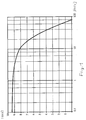
- Fig. 1 shows the typical dynamic resolution (effective number of bits ENB) of a 10 bit ADC versus the input frequency.
- the depicted tuner concept in Fig. 2 is based on a double conversion tuner having a high first IF frequency region.
- a tuner input receives from an antenna Ant e.g. input frequencies in the range 40 ... 900MHz.
- a first controllable bandpass BP1 selects e.g. a TV channel. Its output signal is mixed in a mixing stage M1 with the output frequency of a first local oscillator LO1 which serves in connection with BP1 to select a channel.
- the resulting output signal passes a second bandpass BP2 forming a first IF signal and is amplified in a first IF amplifier stage V1.
- the first IF signal lies in the range 1 ... 2GHz.
- the first IF signal then passes through two parallel chains.
- Chain A comprises:
- Chain B comprises:
- IF analogue (f) S if (f) + S -if (f) , with S if (f) for f ⁇ 0, and S -if (f) for f ⁇ 0 .
- f PC is the picture carrier.
- LP 2A /LP 2B After lowpass filtering (output LP 2A /LP 2B ) all RF signal components disappear.
- Fig. 3 has only given a simplified illustration of the conversion process which needs now to be considered with a closer look at the actual spectra in the analogue IF domain.
- ABFI is the assumed bandwidth of the first IF signal.
- the analogue IF signal is down-converted to zero-frequency according to Fig. 4c, if in Fig. 4a the picture carrier fpc is taken as a reference which is not a necessary condition. Due to the non-symmetric spectra of the VSB-signals an overlapping of originally different frequency components takes place in the baseband region. The mixing causes also down-converted negative frequency components, which are not depicted in Fig. 4. As a result of this down-conversion, beyond 1MHz different frequency components will overlap as illustrated in Fig. 4c. The dashed line shows a quadrature component like frequency component. These erroneous frequency components can only be removed or compensated by adding the quadrature component later on as described above with reference to Fig. 3.
- the whole conversion process has to be carried out with high linearity in order to enable a compensation of the erroneous frequency components in the digital domain.
- the dynamic resolution of the ADCs will play a major role in this respect, but also the amplitude linearity of the in-phase and quadrature mixer stages M 2A and M 2B .
- prefilter LP 2A and LP 2B for the ADCs simple low-cost lowpass filters LPP (see Fig. 4d) can be applied to suppress the RF signal components.
- the resulting ADC input signals of Fig. 4e and Fig. 5a consist not only of the wanted signal but also of a superposition of adjacent channel signals.
- the wanted signal will encounter in the temporal domain a dynamic range of the ADC reduced by a factor of at least 2, more likely of 4.
- the digitising of the analogue IF signals requires a resolution of at least 10 bits.
- a large amount of energy is located around the vision carrier.
- sampling frequency f s Another interesting role in this context plays the choice of the sampling frequency f s .
- a sampling frequency f s being 3 or 4 times greater than the channel bandwidth CB is quite advantageous.
- the resulting aliasing in the adjacent channels does not disturb the wanted signal as shown in Fig. 5c.
- the Nyquist point is set to f s /4, an advantageous low number of coefficients is required for the Nyquist filter.
- a higher sampling frequency also allows a higher dynamic resolution in connection with digital post-filtering.
- An AGC control of the zero-frequency IF signals at the input of the ADCs is advantageous in order to utilise the full dynamic range of the ADCs A/D A and A/D B .
Abstract
Usual A/D converters are not suited for digitising video IF signals because video signals have a much higher bandwidth and because video signals are vestigal-sideband modulated.
The inventive analogue-to-digital conversion circumvents the low dynamic resolution problem of the ADC and allows the application of low-cost ADCs. The problem of low dynamic range with IF digitising can be overcome by combining the basic super-heterodyne principle and the digitising of an in-phase and a quadrature component of a zero-IF and by using a reduced sampling clock for the ADCs.
The inventive analogue-to-digital conversion circumvents the low dynamic resolution problem of the ADC and allows the application of low-cost ADCs. The problem of low dynamic range with IF digitising can be overcome by combining the basic super-heterodyne principle and the digitising of an in-phase and a quadrature component of a zero-IF and by using a reduced sampling clock for the ADCs.
Description
- The present invention relates to a method and to an apparatus for IF demodulation of a high frequency input signal.
- The use of digital signal processing in modern TV receiver design should allow to perform many of signal conditioning, filtering and demodulation functions in a more flexible and economical way as it is the case today with analogue components, thus, conferring an improved performance.
The digital processing starts with an A/D conversion, if possible, it should include the IF processing. The digitising of audio IF signals is known from "Undersampling Techniques Simplifying Digital Radio", Electronics Design 67, May 23, 1991.
But such techniques are not suitable for video IF signals for two reasons: - video signals have a much higher bandwidth,
- video signals are vestigal-sideband modulated (VSB).
- It is one object of the invention to disclose a method of digitising video IF signals using existing A/D converters. This object is reached by the method disclosed in
claim 1. - It is a further object of the invention to disclose an apparatus which utilises the inventive method. This object is reached by the apparatus disclosed in
claim 9. - At present, the ADC technology can be considered as a principal constraint to the advancement of digitally implemented concepts in the IF part of an TV receiver. Although this area of technology is undergoing a rapid development it cannot be expected that in the next years low-cost ADCs will come on the market which can meet the requirements for such digital TV processing. The inventive analogue-to-digital conversion architecture circumvents the ADC problems and allows the application of low-cost ADCs. The invention allows digitising of VSB modulated IF signals of high bandwidth, e.g. TV signals.
The potential achievements of a subsequent digital processing may be summarised as: - a reduction in the complexity of analogue elements of the design;
- the ability to re-configure a TV receiver or VCR, without any increase in hardware, to a variety of different TV standards;
- the ability to provide a range of tailored filter functions (f.i. sound trap);
- the ability to apply on-line correction algorithms (AGC, AFC, etc.);
- the application of novel demodulation techniques.
- In principle the inventive method is suited for IF demodulation of a high frequency input signal, wherein a first mixing stage and first local oscillator means and first filter means are used to generate a first IF signal and wherein that said first IF signal is formed in two parallel branches to an in-phase component of a second IF signal and to a quadrature component of said second IF signal using second local oscillator means and wherein said in-phase component and said quadrature component are each A/D converted and are re-modulated and combined in the digital domain using a third local oscillator means and combining means, thereby forming a digital IF signal.
- Advantageous additional embodiments of the inventive method are resulting from the respective dependent claims.
- In principle the inventive apparatus for IF demodulation of a high frequency input signal comprises:
- a first mixing stage and first local oscillator means and first filter means which are used to generate a first IF signal;
- subsequently, two parallel branches which each comprises a further mixing stage and further filter means and which form from said first IF signal an in-phase component of a second IF signal and a quadrature component of said second IF signal using second local oscillator means and first 90° phase shifting means;
- A/D converting means which convert said in-phase component and said quadrature component to the digital domain;
- subsequently, further mixing stages which re-modulate each of said components in the digital domain using third local oscillator means and second 90° phase shifting means;
- combining means which form from said re-modulated components a digital IF signal.
- Advantageous additional embodiments of the inventive apparatus are resulting from the respective dependent claim.
- Preferred embodiments of the invention are described with reference to the accompanying drawings, which show in:
- Fig. 1
- dynamic resolution of a flash A/D converter;
- Fig. 2
- principle of inventive tuner with digital IF;
- Fig. 3
- inventive conversion from the analogue IF to a digital IF signal;
- Fig. 4
- continuation of Fig. 3;
- Fig. 5
- aliasing in the digitised IF signal.
- Fig. 1 shows the typical dynamic resolution (effective number of bits ENB) of a 10 bit ADC versus the input frequency.
- The depicted tuner concept in Fig. 2 is based on a double conversion tuner having a high first IF frequency region. A tuner input receives from an antenna Ant e.g. input frequencies in the range 40 ... 900MHz. A first controllable bandpass BP₁ selects e.g. a TV channel. Its output signal is mixed in a mixing stage M₁ with the output frequency of a first local oscillator LO₁ which serves in connection with BP₁ to select a channel. The resulting output signal passes a second bandpass BP₂ forming a first IF signal and is amplified in a first IF amplifier stage V₁. Advantageously, the first IF signal lies in the
range 1 ... 2GHz.
The first IF signal then passes through two parallel chains.
Chain A comprises: - a second mixing stage M2A which receives as second input the signal of a second local oscillator LO₂ the frequency of which leads to a zero-IF;
- a first low pass LP2A which delivers the in-phase IF component;
- a second IF amplifier V2A which can be AGC controlled;
- a first A/D converter A/DA which is clocked with the sampling frequency fs;
- a third mixer stage M3A which receives as second input the signal of a third local oscillator LO₃ and which delivers a first component of the final digital IF signal IFdig.
- Chain B comprises:
- a fourth mixing stage M2B which receives as second input the signal of the second local oscillator LO₂ after having passed through a first 90° phase shifter PHS₂;
- a second low pass LP2B which delivers the quadrature IF component;
- a third IF amplifier V2B which can be AGC controlled;
- a second A/D converter A/DB which is clocked with the same sampling frequency fs;
- a fifth mixer stage M3B which receives as second input the signal of the third local oscillator LO₃ after having passed through a second 90° phase shifter PHS₃. M3B delivers a second component of the final digital IF signal IFdig.
- This tuner concept offers two considerable advantages:
- Firstly, the image response filtering becomes trivial, that means the lowest image frequency is located beyond 2GHz;
- Secondly, the synthesiser LO₁ needs only to tune less than one octave.
- An explanation of the analogue-to-digital conversion of the IF signal in the frequency domain is depicted in Fig. 3. Given the spectrum of the first IF signal (output of V₁) by (Fig. 3a):

with Sif(f) for f≧0, and S-if(f) for f<0 . fPC is the picture carrier.
The output signals of the in-phase and quadrature mixer stage (output M2A/M2B) are:

and

After lowpass filtering (output LP2A/LP2B) all RF signal components disappear. Therefore, the input signals of the ADCs are:

and

Because assuming that no aliasing will occur in the digitising process, the mathematical description of the sampling process is ignored for the sake of simplicity. - The complex re-modulation by means of the local oscillator frequency LO₃ in the digital domain yields then:

and

After superposing the resulting in-phase and quadrature component the original but frequency shifted IF signal is reconstructed according to Fig. 3f:

Advantageously, the location on the f axis does not matter in the digital domain. - The above considered concept offers a large scope in choosing the sampling frequency fs and the digital local oscillator frequency LO₃. This is a quite welcome feature if one regards the succeeding filter applications like Nyquist-filtering of a VSB-AM modulated video signal.
Fig. 3 has only given a simplified illustration of the conversion process which needs now to be considered with a closer look at the actual spectra in the analogue IF domain. In order to regard more or less the worst case condition, beside the wanted signal spectrum also the adjacent channel signals have to be included into the consideration as shown in Fig. 4a. ABFI is the assumed bandwidth of the first IF signal. By means of local oscillator frequency LO₂ depicted in Fig. 4b
the analogue IF signal is down-converted to zero-frequency according to Fig. 4c, if in Fig. 4a the picture carrier fpc is taken as a reference which is not a necessary condition. Due to the non-symmetric spectra of the VSB-signals an overlapping of originally different frequency components takes place in the baseband region. The mixing causes also down-converted negative frequency components, which are not depicted in Fig. 4. As a result of this down-conversion, beyond 1MHz different frequency components will overlap as illustrated in Fig. 4c. The dashed line shows a quadrature component like frequency component. These erroneous frequency components can only be removed or compensated by adding the quadrature component later on as described above with reference to Fig. 3.
The whole conversion process has to be carried out with high linearity in order to enable a compensation of the erroneous frequency components in the digital domain. As stated above, the dynamic resolution of the ADCs will play a major role in this respect, but also the amplitude linearity of the in-phase and quadrature mixer stages M2A and M2B.
As prefilter LP2A and LP2B for the ADCs, simple low-cost lowpass filters LPP (see Fig. 4d) can be applied to suppress the RF signal components. The resulting ADC input signals of Fig. 4e and Fig. 5a consist not only of the wanted signal but also of a superposition of adjacent channel signals. Therefore, the wanted signal will encounter in the temporal domain a dynamic range of the ADC reduced by a factor of at least 2, more likely of 4.
Taking an 8 bit resolution of the CVBS signal after demodulation as a minimum requirement, the digitising of the analogue IF signals requires a resolution of at least 10 bits. Normally, a large amount of energy is located around the vision carrier. Thus, it seems reasonable to use a prefilter LPN having notches at the adjacent channel vision carrier frequencies, but this requirement would also complicate the prefilter and consequently increase the costs. A trade-off between the available dynamic resolution of the ADC on one hand and the complexity of the prefilter on the other hand becomes discernible. - Another interesting role in this context plays the choice of the sampling frequency fs. According to Fig. 5b, a sampling frequency fs being 3 or 4 times greater than the channel bandwidth CB is quite advantageous. In this case, the resulting aliasing in the adjacent channels does not disturb the wanted signal as shown in Fig. 5c.
If in case of Nyquist-filtering the Nyquist point is set to fs/4, an advantageous low number of coefficients is required for the Nyquist filter.
Taking not into account the non-linear behaviour of the ADC's quantisation characteristic, a higher sampling frequency (over-sampling) also allows a higher dynamic resolution in connection with digital post-filtering.
Because large signal amplitudes in the adjacent channels coming from a TV transmitter nearby may be mixed into the zero-IF by phase noise components of the local oscillator, the quality of the local oscillator LO₂ will affect the overall performance of the digitising process.
An AGC control of the zero-frequency IF signals at the input of the ADCs is advantageous in order to utilise the full dynamic range of the ADCs A/DA and A/DB. - Similarly, a 10 or more bit analogue-to-digital conversion of a modulated audio signal which occupies only a small part of the amplitude range of the IF signal will not lead to satisfactory results. Therefore, a parallel architecture for the sound demodulation can be used.
Claims (10)
- Method for IF demodulation of a high frequency input signal, wherein a first mixing stage (M₁) and first local oscillator means (LO₁) and first filter means (BP₁, BP₂) are used to generate a first IF signal, characterised in that said first IF signal is formed in two parallel branches (M2A, LP2A; M2B, LP2B) to an in-phase component (Min-phase) of a second IF signal and to a quadrature component (Mquadrature) of said second IF signal using second local oscillator means (LO₂), wherein said in-phase component and said quadrature component are each A/D converted (A/DA, A/DB) and are re-modulated and combined in the digital domain using a third local oscillator means (LO₃) and combining means (A), thereby forming a digital IF signal (IFdig).
- Method according to claim 1, characterised in that said high frequency input signal is a vestigal-sideband modulated signal, especially an UHF TV signal.
- Method according to claim 1 or 2, characterised in that said second local oscillator means (LO₂) have a frequency which leads principally to a zero-IF for said second IF signal.
- Method according to any of claims 1 to 3, characterised in that the sampling frequency (fs) used in said A/D conversion (A/DA, A/DB) is a multiple - especially three or four - of the channel bandwidth (CB) of said high frequency input signal.
- Method according to any of claims 1 to 4, characterised in that each of said parallel branches comprises a further mixing stage (M2A, M2B) and further filter means (LP2A, LP2B).
- Method according to any of claims 1 to 5, characterised in that each of said parallel branches comprises AGC controlled amplifier means (V2A, V2B) causing a subsequent full range A/D conversion.
- Method according to any of claims 1 to 6, characterised in that said quadrature component is formed (M2B) using first 90° phase shifting means (PHS₂) and that the re-modulation of said quadrature component is performed (M3B) using second 90° phase shifting means (PHS₃)
- Method according to any of claims 4 to 7, characterised in that a Nyquist-filtering is performed on said digital IF signal (IFdig), wherein the Nyquist point is set to one quarter of said sampling frequency (fs).
- Apparatus for IF demodulation of a high frequency input signal, related to a method according to any of claims 1 to 8 and comprising:- a first mixing stage (M₁) and first local oscillator means (LO₁) and first filter means (BP₁, BP₂) which are used to generate a first IF signal;- subsequently, two parallel branches which each comprises a further mixing stage (M2A, M2B) and further filter means (LP2A, LP2B) and which form from said first IF signal an in-phase component (Min-phase) of a second IF signal and a quadrature component (Mquadrature) of said second IF signal using second local oscillator means (LO₂) and first 90° phase shifting means (PHS₂);- A/D converting means (A/DA, A/DB) which convert said in-phase component and said quadrature component to the digital domain;- subsequently, further mixing stages (M3A, M3B) which re-modulate each of said components in the digital domain using third local oscillator means (LO₃) and second 90° phase shifting means (PHS₃);- combining means (A) which form from said re-modulated components a digital IF signal (IFdig).
- Apparatus according to claim 9, characterised in that said second local oscillator means (LO₂) have a frequency which leads principally to a zero-IF for said second IF signal
Priority Applications (1)
| Application Number | Priority Date | Filing Date | Title |
|---|---|---|---|
| EP93401480A EP0629040A1 (en) | 1993-06-10 | 1993-06-10 | Method and apparatus for IF demodulation of a high frequency input signal |
Applications Claiming Priority (1)
| Application Number | Priority Date | Filing Date | Title |
|---|---|---|---|
| EP93401480A EP0629040A1 (en) | 1993-06-10 | 1993-06-10 | Method and apparatus for IF demodulation of a high frequency input signal |
Publications (1)
| Publication Number | Publication Date |
|---|---|
| EP0629040A1 true EP0629040A1 (en) | 1994-12-14 |
Family
ID=8214723
Family Applications (1)
| Application Number | Title | Priority Date | Filing Date |
|---|---|---|---|
| EP93401480A Withdrawn EP0629040A1 (en) | 1993-06-10 | 1993-06-10 | Method and apparatus for IF demodulation of a high frequency input signal |
Country Status (1)
| Country | Link |
|---|---|
| EP (1) | EP0629040A1 (en) |
Cited By (8)
| Publication number | Priority date | Publication date | Assignee | Title |
|---|---|---|---|---|
| EP0744865A2 (en) * | 1995-05-23 | 1996-11-27 | THOMSON multimedia | Method for digitising a signal at intermediate frequency particularly a television signal, and circuit for implementing the same |
| FR2735316A1 (en) * | 1995-06-12 | 1996-12-13 | Thomson Multimedia Sa | METHOD FOR DIGITIZING FI VIDEO SIGNALS AND DEVICE FOR CARRYING OUT SAID METHOD |
| WO1999038269A1 (en) * | 1998-01-22 | 1999-07-29 | Infineon Technologies Ag | Circuit for demodulating two-dimensional data symbols transmitted by means of supported data transmission |
| WO2000028664A2 (en) * | 1998-11-12 | 2000-05-18 | Broadcom Corporation | Fully integrated tuner architecture |
| CN1067193C (en) * | 1995-02-16 | 2001-06-13 | 皇家菲利浦电子有限公司 | Improvement in or relating to communications receivers |
| US6426680B1 (en) | 1999-05-26 | 2002-07-30 | Broadcom Corporation | System and method for narrow band PLL tuning |
| US6696898B1 (en) | 1998-11-12 | 2004-02-24 | Broadcom Corporation | Differential crystal oscillator |
| US6885275B1 (en) | 1998-11-12 | 2005-04-26 | Broadcom Corporation | Multi-track integrated spiral inductor |
Citations (3)
| Publication number | Priority date | Publication date | Assignee | Title |
|---|---|---|---|---|
| EP0151281A1 (en) * | 1984-02-03 | 1985-08-14 | Licentia Patent-Verwaltungs-GmbH | Time-multiplex digital cellular radio system |
| EP0255553A1 (en) * | 1986-08-07 | 1988-02-10 | Deutsche ITT Industries GmbH | Method for receiving frequency-modulated stereo-multiplex signals |
| US5003621A (en) * | 1989-11-02 | 1991-03-26 | Motorola, Inc. | Direct conversion FM receiver |
-
1993
- 1993-06-10 EP EP93401480A patent/EP0629040A1/en not_active Withdrawn
Patent Citations (3)
| Publication number | Priority date | Publication date | Assignee | Title |
|---|---|---|---|---|
| EP0151281A1 (en) * | 1984-02-03 | 1985-08-14 | Licentia Patent-Verwaltungs-GmbH | Time-multiplex digital cellular radio system |
| EP0255553A1 (en) * | 1986-08-07 | 1988-02-10 | Deutsche ITT Industries GmbH | Method for receiving frequency-modulated stereo-multiplex signals |
| US5003621A (en) * | 1989-11-02 | 1991-03-26 | Motorola, Inc. | Direct conversion FM receiver |
Cited By (29)
| Publication number | Priority date | Publication date | Assignee | Title |
|---|---|---|---|---|
| CN1067193C (en) * | 1995-02-16 | 2001-06-13 | 皇家菲利浦电子有限公司 | Improvement in or relating to communications receivers |
| FR2734681A1 (en) * | 1995-05-23 | 1996-11-29 | Thomson Multimedia Sa | PROCESS FOR DIGITIZING AN INTERMEDIATE FREQUENCY SIGNAL IF, IN PARTICULAR TELEVISION, AND CIRCUIT FOR IMPLEMENTING THIS PROCEDURE |
| EP0744865A3 (en) * | 1995-05-23 | 1996-12-04 | THOMSON multimedia | Method for digitising a signal at intermediate frequency particularly a television signal, and circuit for implementing the same |
| US5748262A (en) * | 1995-05-23 | 1998-05-05 | Thomson Multimedia S.A. | Method of digitization of intermediate frequency signals in particular television signals, and device for implementation of the method |
| EP0744865A2 (en) * | 1995-05-23 | 1996-11-27 | THOMSON multimedia | Method for digitising a signal at intermediate frequency particularly a television signal, and circuit for implementing the same |
| FR2735316A1 (en) * | 1995-06-12 | 1996-12-13 | Thomson Multimedia Sa | METHOD FOR DIGITIZING FI VIDEO SIGNALS AND DEVICE FOR CARRYING OUT SAID METHOD |
| EP0749237A1 (en) * | 1995-06-12 | 1996-12-18 | THOMSON multimedia S.A. | Method for digitising video signals at intermediate frequency and apparatus for implementing the same |
| US5831689A (en) * | 1995-06-12 | 1998-11-03 | Thomson Multimedia S.A. | Method of digitization of intermediate frequency video signals and device for implementation of the method |
| US6424683B1 (en) | 1998-01-22 | 2002-07-23 | Infineon Technologies Ag | Circuit for demodulating two-dimensional data symbols transmitted by a carrier-based data transmission |
| WO1999038269A1 (en) * | 1998-01-22 | 1999-07-29 | Infineon Technologies Ag | Circuit for demodulating two-dimensional data symbols transmitted by means of supported data transmission |
| US6591091B1 (en) | 1998-11-12 | 2003-07-08 | Broadcom Corporation | System and method for coarse/fine PLL adjustment |
| US6963248B2 (en) | 1998-11-12 | 2005-11-08 | Broadcom Corporation | Phase locked loop |
| WO2000028664A3 (en) * | 1998-11-12 | 2001-07-26 | Broadcom Corp | Fully integrated tuner architecture |
| US8227892B2 (en) | 1998-11-12 | 2012-07-24 | Broadcom Corporation | Multi-track integrated circuit inductor |
| WO2000028664A2 (en) * | 1998-11-12 | 2000-05-18 | Broadcom Corporation | Fully integrated tuner architecture |
| US6696898B1 (en) | 1998-11-12 | 2004-02-24 | Broadcom Corporation | Differential crystal oscillator |
| US8195117B2 (en) | 1998-11-12 | 2012-06-05 | Broadcom Corporation | Integrated switchless programmable attenuator and low noise amplifier |
| US6879816B2 (en) | 1998-11-12 | 2005-04-12 | Broadcom Corporation | Integrated switchless programmable attenuator and low noise amplifier |
| US6885275B1 (en) | 1998-11-12 | 2005-04-26 | Broadcom Corporation | Multi-track integrated spiral inductor |
| US6377315B1 (en) | 1998-11-12 | 2002-04-23 | Broadcom Corporation | System and method for providing a low power receiver design |
| US7019598B2 (en) | 1998-11-12 | 2006-03-28 | Broadcom Corporation | Integrated VCO having an improved tuning range over process and temperature variations |
| US7199664B2 (en) | 1998-11-12 | 2007-04-03 | Broadcom Corporation | Integrated switchless programmable attenuator and low noise amplifier |
| US7366486B2 (en) | 1998-11-12 | 2008-04-29 | Broadcom Corporation | System and method for coarse/fine PLL adjustment |
| US7719083B2 (en) | 1998-11-12 | 2010-05-18 | Broadcomm Corporation | Integrated spiral inductor |
| US7729676B2 (en) | 1998-11-12 | 2010-06-01 | Broadcom Corporation | Integrated switchless programmable attenuator and low noise amplifier |
| US7821581B2 (en) | 1998-11-12 | 2010-10-26 | Broadcom Corporation | Fully integrated tuner architecture |
| US8045066B2 (en) | 1998-11-12 | 2011-10-25 | Broadcom Corporation | Fully integrated tuner architecture |
| US6803829B2 (en) | 1999-05-26 | 2004-10-12 | Broadcom Corporation | Integrated VCO having an improved tuning range over process and temperature variations |
| US6426680B1 (en) | 1999-05-26 | 2002-07-30 | Broadcom Corporation | System and method for narrow band PLL tuning |
Similar Documents
| Publication | Publication Date | Title |
|---|---|---|
| AU700076B2 (en) | Radio frequency signal reception using frequency shifting by discrete-time sub-sampling down-conversion | |
| US5483695A (en) | Intermediate frequency FM receiver using analog oversampling to increase signal bandwidth | |
| JP2546741B2 (en) | Cable television. Homodyne receiving system for converter and its device | |
| US6895232B2 (en) | Method and apparatus for receiving radio frequency signals | |
| EP0629040A1 (en) | Method and apparatus for IF demodulation of a high frequency input signal | |
| KR20060052603A (en) | Method and circuit for channel filtering of analog or digitally modulated tv signals | |
| US6324233B1 (en) | Reception of modulated carriers having asymmetrical sidebands | |
| KR100335639B1 (en) | Digital television tuner | |
| US7599010B2 (en) | TV receiver and analog TV signal processing method | |
| US4870480A (en) | Subnyquist demodulator as for a television receiver | |
| US4395734A (en) | Remote muting for CATV/STV converters | |
| EP0959559B1 (en) | Direct broadcast satellite tuner | |
| JP2004531967A (en) | Down converter | |
| JP4270649B2 (en) | Frequency converter for television signals | |
| US7145610B2 (en) | Receiving method and apparatus of analog television signals technical field | |
| US7266350B2 (en) | Radio frequency tuner | |
| US20020011904A1 (en) | Low cost digital FM modulator | |
| JP2000068752A (en) | Receiver for digital broadcasting | |
| JP2000092021A (en) | Digital broadcast receiver | |
| GB2349783A (en) | Receiver circuit using sub sampling analogue to digital converter to frequency shift the signal | |
| Coy et al. | HF-band radio receiver design based on digital signal processing | |
| JP3495661B2 (en) | Receiver | |
| JP3038280B2 (en) | Receiver | |
| JP3495656B2 (en) | Receiver | |
| JPH0888578A (en) | Receiver for broadcasting adapted to analog and digital signals |
Legal Events
| Date | Code | Title | Description |
|---|---|---|---|
| PUAI | Public reference made under article 153(3) epc to a published international application that has entered the european phase |
Free format text: ORIGINAL CODE: 0009012 |
|
| AK | Designated contracting states |
Kind code of ref document: A1 Designated state(s): DE ES FR GB IT |
|
| RAP1 | Party data changed (applicant data changed or rights of an application transferred) |
Owner name: THOMSON MULTIMEDIA |
|
| 17P | Request for examination filed |
Effective date: 19950506 |
|
| 17Q | First examination report despatched |
Effective date: 19970120 |
|
| RAP1 | Party data changed (applicant data changed or rights of an application transferred) |
Owner name: THOMSON MULTIMEDIA |
|
| STAA | Information on the status of an ep patent application or granted ep patent |
Free format text: STATUS: THE APPLICATION IS DEEMED TO BE WITHDRAWN |
|
| 18D | Application deemed to be withdrawn |
Effective date: 19980929 |