EP0634701A1 - Exposure apparatus, and manufacturing method for devices using same - Google Patents
Exposure apparatus, and manufacturing method for devices using same Download PDFInfo
- Publication number
- EP0634701A1 EP0634701A1 EP94305113A EP94305113A EP0634701A1 EP 0634701 A1 EP0634701 A1 EP 0634701A1 EP 94305113 A EP94305113 A EP 94305113A EP 94305113 A EP94305113 A EP 94305113A EP 0634701 A1 EP0634701 A1 EP 0634701A1
- Authority
- EP
- European Patent Office
- Prior art keywords
- pattern
- mask
- writing error
- writing
- exposure
- Prior art date
- Legal status (The legal status is an assumption and is not a legal conclusion. Google has not performed a legal analysis and makes no representation as to the accuracy of the status listed.)
- Granted
Links
Images


Classifications
-
- H—ELECTRICITY
- H01—ELECTRIC ELEMENTS
- H01L—SEMICONDUCTOR DEVICES NOT COVERED BY CLASS H10
- H01L21/00—Processes or apparatus adapted for the manufacture or treatment of semiconductor or solid state devices or of parts thereof
- H01L21/02—Manufacture or treatment of semiconductor devices or of parts thereof
- H01L21/027—Making masks on semiconductor bodies for further photolithographic processing not provided for in group H01L21/18 or H01L21/34
-
- G—PHYSICS
- G03—PHOTOGRAPHY; CINEMATOGRAPHY; ANALOGOUS TECHNIQUES USING WAVES OTHER THAN OPTICAL WAVES; ELECTROGRAPHY; HOLOGRAPHY
- G03F—PHOTOMECHANICAL PRODUCTION OF TEXTURED OR PATTERNED SURFACES, e.g. FOR PRINTING, FOR PROCESSING OF SEMICONDUCTOR DEVICES; MATERIALS THEREFOR; ORIGINALS THEREFOR; APPARATUS SPECIALLY ADAPTED THEREFOR
- G03F7/00—Photomechanical, e.g. photolithographic, production of textured or patterned surfaces, e.g. printing surfaces; Materials therefor, e.g. comprising photoresists; Apparatus specially adapted therefor
- G03F7/70—Microphotolithographic exposure; Apparatus therefor
- G03F7/70216—Mask projection systems
- G03F7/70358—Scanning exposure, i.e. relative movement of patterned beam and workpiece during imaging
-
- G—PHYSICS
- G03—PHOTOGRAPHY; CINEMATOGRAPHY; ANALOGOUS TECHNIQUES USING WAVES OTHER THAN OPTICAL WAVES; ELECTROGRAPHY; HOLOGRAPHY
- G03F—PHOTOMECHANICAL PRODUCTION OF TEXTURED OR PATTERNED SURFACES, e.g. FOR PRINTING, FOR PROCESSING OF SEMICONDUCTOR DEVICES; MATERIALS THEREFOR; ORIGINALS THEREFOR; APPARATUS SPECIALLY ADAPTED THEREFOR
- G03F7/00—Photomechanical, e.g. photolithographic, production of textured or patterned surfaces, e.g. printing surfaces; Materials therefor, e.g. comprising photoresists; Apparatus specially adapted therefor
- G03F7/70—Microphotolithographic exposure; Apparatus therefor
- G03F7/70691—Handling of masks or workpieces
- G03F7/70716—Stages
- G03F7/70725—Stages control
Definitions
- the present invention relates to an exposure apparatus and a method of manufacturing devices using the same.
- photolithography is mainly effected by reduction projection exposure apparatus (stepper) having a resolution of submicrons, and a larger numerical aperture (NA) and further reduction of wavelength of the light for the exposure are developed toward further improvement in the resolution.
- stepper reduction projection exposure apparatus
- NA numerical aperture
- One-to-one scanning type exposure apparatus using reflection type projection optical system is improved, for example, there are noted a reduction projection optical system incorporating a refraction element such as lens or the like in a projection optical system to combine with reflection element such as mirror, or a scanning type exposure apparatus in which a reduction projection optical system constituted only by refraction elements are used, and both of a mask stage and a wafer stage are moved in a speed ratio corresponding to the reduction.
- an exposure apparatus having means for correcting the writing error of the pattern.
- the device pattern is transferred onto the member to be exposed using such an exposure apparatus.
- means is provided to detect the pattern writing error on the basis of a position of the device pattern.
- means is provided to detect the pattern writing error on the basis of a position of the positioning mark on the mask.
- a positioning optical system for positioning the mask and the member to be exposed also functions as an optical system for detecting the writing error.
- the writing error of the pattern is corrected while scanning the mask and the member to be exposed with an exposure beam.
- Figure 1 is a schematic view illustrating an apparatus according to an embodiment of the present invention.
- FIG. 1 illustrates scanning exposure in the apparatus of Figure 1.
- Figure 3 is a flow chart for manufacturing a semiconductor device.
- Figure 4 shows a wafer process of Figure 3.
- Figure 1 shows a scanning exposure apparatus according to an embodiment of the present invention, for manufacturing semiconductor devices or devices such as CCD, liquid crystal panel, magnetic head or the like.
- a mask 1 having a written pattern is supported in a main assembly on a mask stage 4 driven and controlled in XY direction by control means 103 and laser interferometer (not shown).
- the mask 1 and the wafer 3 are located optically conjugate position through the projection optical system 2.
- a slit-like exposure beam 6 extending in Y direction from an unshown illumination system is projected on the mask 1, and the pattern of the mask 1 is imaged on a wafer 3 with a scale corresponding to the projection magnification of the projection optical system.
- both of the mask stage 4 and the wafer stage 5 are moved in X direction at a speed ratio corresponding to the projection magnification of the projection optical system 2 relative to the slit exposure beam 6, so that the relative scanning is effected between the mask 1 and the wafer 3.
- the entirety of the device pattern 21 of the mask 3 is transferred onto a transfer region (pattern region) 22 of the wafer 3.
- the projection optical system 2 may be constituted only by refraction elements or by both of reflection elements and refraction element.
- the mask 1 is supported on a mask stage 4, and the state of pattern writing of the device pattern or the like on the mask 1 is measured. More particularly, a plurality of mask writing evaluation marks 51 (written together with the device pattern) arranged in XY directions on the mask 1, are observed by a pair of observing microscopes 7. A signal relating to mark 51 position obtained by the microscopes 7 is processed by mark detecting means 101, and the output thereof is transmitted to a processing circuit 102 as position information of the mask writing evaluation mark. The position of the mask stage 4 during the observation is measured by an unshown laser interferometer. The information relating to the position of the stage 4, is transmitted to a processing circuit 102 by drive control means 103, and is stored corresponding to the position information for the mask writing evaluation mark 51.
- the measurement is repeated for the plurality of mask writing evaluation marks 51, while controlling the position of the mask stage 4 using a laser interferometer (not shown), by which writing state of the mask pattern on the mask 1 is discriminated.
- the mask writing evaluation marks 51 are written by an electron beam writing device simultaneously with the device pattern 21, and therefore, represent original position of the pattern 21, writing magnification (size) and/or the perpendicularity of the pattern. Therefore, when the writing magnification or the perpendicularity are to be measured, at least three mask writing evaluation marks 51 are required.
- the mask writing evaluation marks 51 are disposed in the manner of enclosing the device pattern 21. However, they may be disposed in the pattern 21 region. The configuration of the mark is not limited to "cross".
- the device pattern 21 may be used as the mark.
- a scanning driving method for correcting the detected writing error is instructed to the drive control means 103 from processing circuit 102 storing the writing state (error) of the pattern 21.
- the relative position between the mask stage 4 and the wafer stage 5 is controlled to correct the writing error, and therefore, the pattern 21 is transferred onto the transfer region 22 on the wafer with high accuracy.
- the processing circuit 102 instructs the drive control means 103 the scanning drive method for correcting the perpendicularity error ⁇ . More particularly, the mask stage 4 is driven inclinedly by the degree corresponding to the perpendicularity error ⁇ , relative to the scanning direction (X) of the wafer stage 5.
- the mask stage 4 and the wafer stage 5 are moved relative to the slit exposure light 6 as shown in Figures 2B - 2D, while controlling the positions using an unshown laser interferometer. As a result, the transfer region 22 is exposed to the pattern 21 with the writing error corrected. Therefore, the patterns 21 and 22 can be overlaid with high precision.
- the observation microscopes 7 in this embodiment may be used also as alignment optical system for detecting positional deviation between the mask 1 and the wafer 3.
- the position of the mask writing evaluation marks 51 is also detected.
- the writing evaluation mark 51 of the mask 1 may be used also as the mask alignment mark, advantageously.
- FIG. 3 is a flow chart of manufacturing semiconductor devices such as IC, LSI or the like, or devices such as liquid crystal panel or CCD or the like.
- step 1 circuit design
- step 2 the mask having the designed circuit pattern is manufactured.
- step 3 a wafer is manufactured using the proper material such as silicon.
- step 4 is called pre-step, in which actual circuit pattern is formed on a wafer through lithographic technique using the prepared mask and wafer.
- step 5 post-step
- a semiconductor chip is manufactured from the wafer subjected to the operations of step 4.
- the step 5 includes assembling steps (dicing, bonding), packaging step (chip sealing) or the like.
- step 6 the operation of the semiconductor device manufactured by the step 5 is inspected, and durability test thereof is carried out. In this manner, the semiconductor device is manufactured and delivered at step 7.
- FIG. 4 is a flow chart of detailed wafer processing.
- the surface of the wafer is oxidized.
- step 12 CVD
- an insulating film is formed on a surface of the wafer.
- step 13 electrode formation
- an electrode is formed on the wafer by evaporation.
- step 14 ion injection
- the ion is implemented into the wafer.
- step 15 resist processing
- a photosensitive material is applied on the wafer.
- the circuit pattern of the mask is projected onto the wafer by the above-described exposure apparatus.
- the exposed wafer is developed.
- step 18 etching
- the portion outside the resist image are removed.
- step 19 resist removal
- the resist is removed after the etching.
- a highly integrated circuit pattern can be formed in the semiconductor devices or the like.
Abstract
Description
- The present invention relates to an exposure apparatus and a method of manufacturing devices using the same.
- The recent progress of the semiconductor device manufacturing and the fine processing related thereto are remarkable. Particularly, photolithography is mainly effected by reduction projection exposure apparatus (stepper) having a resolution of submicrons, and a larger numerical aperture (NA) and further reduction of wavelength of the light for the exposure are developed toward further improvement in the resolution.
- One-to-one scanning type exposure apparatus using reflection type projection optical system is improved, for example, there are noted a reduction projection optical system incorporating a refraction element such as lens or the like in a projection optical system to combine with reflection element such as mirror, or a scanning type exposure apparatus in which a reduction projection optical system constituted only by refraction elements are used, and both of a mask stage and a wafer stage are moved in a speed ratio corresponding to the reduction.
- As a factor influencing alignment between a mask pattern and a wafer pattern, there is a deviation of EB writing (electron beam writing) of the mask pattern (original) from design pattern. Conventionally, the deviation has been ignored because the amount of deviation is small.
- Accordingly, it is an object of the present invention to provide an exposure apparatus and a method of manufacturing devices such as IC, LSI or other semiconductor devices, CCD, liquid crystal panel, magnetic head or the like using the exposure apparatus, in which the mask pattern involving writing error can be correctly transferred onto a pattern of a member to be exposed.
- According to an aspect of the present invention, there is provided an exposure apparatus having means for correcting the writing error of the pattern.
- In the device manufacturing method according to an aspect of the present invention, the device pattern is transferred onto the member to be exposed using such an exposure apparatus.
- According to another aspect of the present invention, means is provided to detect the pattern writing error on the basis of a position of the device pattern.
- According to a further aspect of the present invention, means is provided to detect the pattern writing error on the basis of a position of the positioning mark on the mask.
- According to a further aspect of the present invention, a positioning optical system for positioning the mask and the member to be exposed also functions as an optical system for detecting the writing error.
- According to a further aspect of the present invention, the writing error of the pattern is corrected while scanning the mask and the member to be exposed with an exposure beam.
- These and other objects, features and advantages of the present invention will become more apparent upon a consideration of the following description of the preferred embodiments of the present invention taken in conjunction with the accompanying drawings.
- Figure 1 is a schematic view illustrating an apparatus according to an embodiment of the present invention.
- Figure 2 illustrates scanning exposure in the apparatus of Figure 1.
- Figure 3 is a flow chart for manufacturing a semiconductor device.
- Figure 4 shows a wafer process of Figure 3.
- The preferred embodiments of the present invention will be described in conjunction with the accompanying drawings. Figure 1 shows a scanning exposure apparatus according to an embodiment of the present invention, for manufacturing semiconductor devices or devices such as CCD, liquid crystal panel, magnetic head or the like. A
mask 1 having a written pattern is supported in a main assembly on amask stage 4 driven and controlled in XY direction by control means 103 and laser interferometer (not shown). Themask 1 and thewafer 3 are located optically conjugate position through the projectionoptical system 2. A slit-like exposure beam 6 extending in Y direction from an unshown illumination system is projected on themask 1, and the pattern of themask 1 is imaged on awafer 3 with a scale corresponding to the projection magnification of the projection optical system. For the scanning exposure, both of themask stage 4 and thewafer stage 5 are moved in X direction at a speed ratio corresponding to the projection magnification of the projectionoptical system 2 relative to theslit exposure beam 6, so that the relative scanning is effected between themask 1 and thewafer 3. By this, the entirety of thedevice pattern 21 of themask 3 is transferred onto a transfer region (pattern region) 22 of thewafer 3. The projectionoptical system 2 may be constituted only by refraction elements or by both of reflection elements and refraction element. - In this embodiment, the
mask 1 is supported on amask stage 4, and the state of pattern writing of the device pattern or the like on themask 1 is measured. More particularly, a plurality of mask writing evaluation marks 51 (written together with the device pattern) arranged in XY directions on themask 1, are observed by a pair of observingmicroscopes 7. A signal relating tomark 51 position obtained by themicroscopes 7 is processed by mark detecting means 101, and the output thereof is transmitted to aprocessing circuit 102 as position information of the mask writing evaluation mark. The position of themask stage 4 during the observation is measured by an unshown laser interferometer. The information relating to the position of thestage 4, is transmitted to aprocessing circuit 102 by drive control means 103, and is stored corresponding to the position information for the maskwriting evaluation mark 51. The measurement is repeated for the plurality of maskwriting evaluation marks 51, while controlling the position of themask stage 4 using a laser interferometer (not shown), by which writing state of the mask pattern on themask 1 is discriminated. The maskwriting evaluation marks 51 are written by an electron beam writing device simultaneously with thedevice pattern 21, and therefore, represent original position of thepattern 21, writing magnification (size) and/or the perpendicularity of the pattern. Therefore, when the writing magnification or the perpendicularity are to be measured, at least three maskwriting evaluation marks 51 are required. In this Figure, the maskwriting evaluation marks 51 are disposed in the manner of enclosing thedevice pattern 21. However, they may be disposed in thepattern 21 region. The configuration of the mark is not limited to "cross". Thedevice pattern 21 may be used as the mark. - During the exposure operation, a scanning driving method for correcting the detected writing error is instructed to the drive control means 103 from
processing circuit 102 storing the writing state (error) of thepattern 21. Using an unshown laser interferometer, the relative position between themask stage 4 and thewafer stage 5 is controlled to correct the writing error, and therefore, thepattern 21 is transferred onto thetransfer region 22 on the wafer with high accuracy. - The consideration will be made as to the case in which the
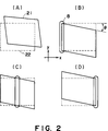
pattern 21 is written with perpendicularity error ϑ, as shown in Figure 2A, for example. Using an unshown alignment system, themask 1 and thewafer 3 are aligned, and thepattern 21 and the scanning start side of thetransfer region 22 are aligned relative to theslit exposure light 6, as shown in Figure 2B. Subsequently, theprocessing circuit 102 instructs the drive control means 103 the scanning drive method for correcting the perpendicularity error ϑ. More particularly, themask stage 4 is driven inclinedly by the degree corresponding to the perpendicularity error ϑ, relative to the scanning direction (X) of thewafer stage 5. Themask stage 4 and thewafer stage 5 are moved relative to theslit exposure light 6 as shown in Figures 2B - 2D, while controlling the positions using an unshown laser interferometer. As a result, thetransfer region 22 is exposed to thepattern 21 with the writing error corrected. Therefore, thepatterns - The
observation microscopes 7 in this embodiment may be used also as alignment optical system for detecting positional deviation between themask 1 and thewafer 3. When the positional deviation between themask 1 and thewafer 3 is detected, the position of the maskwriting evaluation marks 51 is also detected. At this time, thewriting evaluation mark 51 of themask 1 may be used also as the mask alignment mark, advantageously. - The description will be made as to an embodiment of device manufacturing method using the scanning exposure apparatus. Figure 3 is a flow chart of manufacturing semiconductor devices such as IC, LSI or the like, or devices such as liquid crystal panel or CCD or the like. At
step 1, (circuit design), the circuits of the semiconductor device is designed. Atstep 2, the mask having the designed circuit pattern is manufactured. On the other hand, atstep 3, a wafer is manufactured using the proper material such as silicon.Step 4 is called pre-step, in which actual circuit pattern is formed on a wafer through lithographic technique using the prepared mask and wafer. At step 5 (post-step), a semiconductor chip is manufactured from the wafer subjected to the operations ofstep 4. Thestep 5 includes assembling steps (dicing, bonding), packaging step (chip sealing) or the like. Atstep 6, the operation of the semiconductor device manufactured by thestep 5 is inspected, and durability test thereof is carried out. In this manner, the semiconductor device is manufactured and delivered atstep 7. - Figure 4 is a flow chart of detailed wafer processing. At step 11, the surface of the wafer is oxidized. At step 12 (CVD), an insulating film is formed on a surface of the wafer. At step 13 (electrode formation), an electrode is formed on the wafer by evaporation. At step 14 (ion injection), the ion is implemented into the wafer. At step 15 (resist processing), a photosensitive material is applied on the wafer. At step 16 (exposure), the circuit pattern of the mask is projected onto the wafer by the above-described exposure apparatus. At step 17 (development), the exposed wafer is developed. At step 18 (etching), the portion outside the resist image are removed. At step 19 (resist removal), the resist is removed after the etching. By repeating the above-described steps, overlaid circuit patterns are formed on the wafer.
- According to the manufacturing method of the invention, a highly integrated circuit pattern can be formed in the semiconductor devices or the like.
- While the invention has been described with reference to the structures disclosed herein, it is not confined to the details set forth and this application is intended to cover such modifications or changes as may come within the purposes of the improvements or the scope of the following claims.
Claims (17)
- An exposure apparatus comprising:
means for exposing an exposure area of a substrate through a pattern of a mask, wherein said pattern involves writing error; and
means for correcting the writing error of the pattern to correctly overlay the pattern on the exposure region. - An apparatus according to Claim 1, wherein said correcting means includes means for measuring a plurality of portions of a device pattern of the mask, wherein the writing error is detected on the basis of an output of said measuring means.
- An apparatus according to Claim 1, wherein said correcting means including measuring means for measuring positions of a plurality of marks of the mask, wherein the writing error is detected on the basis of an output of said measuring means.
- An apparatus according to Claim 3, wherein the plurality of marks also function as alignment marks for alignment with the substrate.
- An apparatus according to Claim 4, further comprising an alignment optical system for detecting alignment mark.
- An apparatus according to Claim 5, wherein said measuring means and said alignment optical system are partly common.
- An apparatus according to Claim 1, wherein said exposure means includes means for scanning the mask and the substrate relative to an exposure beam.
- An apparatus according to Claim 7, wherein the correcting means controls said scanning means to correct the writing error.
- An apparatus according to Claim 8, wherein when the writing error involves perpendicularity error, said correcting means causes said scanning means to scan the mask and the substrate in different directions.
- An apparatus according to Claim 8, wherein said correcting means includes measuring means for measuring positions of a plurality of portions of a device pattern of the mask and means for detecting writing error on the basis of an output of said measuring means.
- An apparatus according to Claim 8, wherein said correcting means includes measuring means for measuring positions of a plurality of marks of the mask and means for detecting writing error on the basis of an output of said measuring means.
- An apparatus according to Claim 11, wherein the plurality of marks also function as alignment marks for alignment with the substrate.
- An apparatus according to Claim 12, further comprising an alignment optical system for detecting an alignment mark.
- An apparatus according to Claim 13, wherein said measuring means and said alignment optical system are partly common.
- A device manufacturing method using a device pattern involving a writing error, comprising the steps of:
detecting the writing error; and
exposing a pattern area of a substrate while correcting the writing pattern of the device pattern. - A device manufacturing method using a device pattern involving a writing error, comprising the steps of:
detecting a writing error of the device pattern; and
scanning the mask and the substrate with exposure light so as to correct the writing error. - A device manufactured through a method as defined in Claim 15 or 16.
Applications Claiming Priority (2)
| Application Number | Priority Date | Filing Date | Title |
|---|---|---|---|
| JP17431393A JP3210145B2 (en) | 1993-07-14 | 1993-07-14 | Scanning exposure apparatus and method for manufacturing a device using the apparatus |
| JP174313/93 | 1993-07-14 |
Publications (2)
| Publication Number | Publication Date |
|---|---|
| EP0634701A1 true EP0634701A1 (en) | 1995-01-18 |
| EP0634701B1 EP0634701B1 (en) | 1998-09-23 |
Family
ID=15976472
Family Applications (1)
| Application Number | Title | Priority Date | Filing Date |
|---|---|---|---|
| EP94305113A Expired - Lifetime EP0634701B1 (en) | 1993-07-14 | 1994-07-13 | Exposure apparatus, and manufacturing method for devices using same |
Country Status (5)
| Country | Link |
|---|---|
| US (1) | US6268902B1 (en) |
| EP (1) | EP0634701B1 (en) |
| JP (1) | JP3210145B2 (en) |
| KR (1) | KR100222195B1 (en) |
| DE (1) | DE69413465T2 (en) |
Cited By (3)
| Publication number | Priority date | Publication date | Assignee | Title |
|---|---|---|---|---|
| EP0727770A1 (en) * | 1995-02-17 | 1996-08-21 | Aiwa Co., Ltd. | Method and apparatus for aligning miniature device components |
| EP1037266A1 (en) * | 1997-10-07 | 2000-09-20 | Nikon Corporation | Projection exposure method and apparatus |
| US6522390B2 (en) | 1997-10-07 | 2003-02-18 | Nikon Corporation | Projection exposure method and apparatus |
Families Citing this family (11)
| Publication number | Priority date | Publication date | Assignee | Title |
|---|---|---|---|---|
| JPH09320945A (en) * | 1996-05-24 | 1997-12-12 | Nikon Corp | Exposure condition measuring method and aligner |
| JP4198877B2 (en) | 2000-12-25 | 2008-12-17 | 株式会社ルネサステクノロジ | Manufacturing method of semiconductor device |
| JP3495983B2 (en) | 2000-12-28 | 2004-02-09 | キヤノン株式会社 | Mask and projection exposure apparatus |
| JP2002222760A (en) * | 2001-01-29 | 2002-08-09 | Canon Inc | Method and apparatus for exposure and method of manufacturing device |
| EP1482373A1 (en) * | 2003-05-30 | 2004-12-01 | ASML Netherlands B.V. | Lithographic apparatus and device manufacturing method |
| US20050286050A1 (en) * | 2004-06-29 | 2005-12-29 | Nikon Corporation | Real-time through lens image measurement system and method |
| JP4738887B2 (en) * | 2005-05-19 | 2011-08-03 | 株式会社ブイ・テクノロジー | Exposure equipment |
| KR100922549B1 (en) * | 2007-12-24 | 2009-10-21 | 주식회사 동부하이텍 | A misalignment wafer detecting system and a method of detection for a misalignment wafer |
| US8804137B2 (en) * | 2009-08-31 | 2014-08-12 | Kla-Tencor Corporation | Unique mark and method to determine critical dimension uniformity and registration of reticles combined with wafer overlay capability |
| JP2012164811A (en) * | 2011-02-07 | 2012-08-30 | Toshiba Corp | Method of manufacturing semiconductor device, method of determining shipping of exposure mask and method of manufacturing exposure mask |
| CN103324025B (en) * | 2013-06-25 | 2015-08-12 | 北京京东方光电科技有限公司 | Mask plate and apply its detect exposure defect method |
Citations (4)
| Publication number | Priority date | Publication date | Assignee | Title |
|---|---|---|---|---|
| DE3910048A1 (en) * | 1989-03-28 | 1990-08-30 | Heidelberg Instr Gmbh Laser Un | Method for producing or inspecting microstructures on large-area substrates |
| US4958160A (en) * | 1987-08-31 | 1990-09-18 | Canon Kabushiki Kaisha | Projection exposure apparatus and method of correcting projection error |
| US5161114A (en) * | 1989-03-15 | 1992-11-03 | Fujitsu Limited | Method of manufacturing a reticule |
| US5168306A (en) * | 1989-04-04 | 1992-12-01 | Asahi Kogaku Kogyo Kabushiki Kaisha | Exposure apparatus |
Family Cites Families (14)
| Publication number | Priority date | Publication date | Assignee | Title |
|---|---|---|---|---|
| JPS57169244A (en) | 1981-04-13 | 1982-10-18 | Canon Inc | Temperature controller for mask and wafer |
| JPS58108745A (en) | 1981-12-23 | 1983-06-28 | Canon Inc | Erroneous transcription adjusting device |
| JPS58116735A (en) | 1981-12-29 | 1983-07-12 | Canon Inc | Projection printing apparatus |
| US4688932A (en) | 1985-02-12 | 1987-08-25 | Canon Kabushiki Kaisha | Exposure apparatus |
| US5168304A (en) * | 1988-08-22 | 1992-12-01 | Nikon Corporation | Exposure apparatus |
| DE68921687T2 (en) | 1988-09-02 | 1995-08-03 | Canon Kk | Exposure device. |
| JP2627543B2 (en) | 1988-09-05 | 1997-07-09 | キヤノン株式会社 | SOR exposure system |
| JP2890882B2 (en) | 1990-04-06 | 1999-05-17 | キヤノン株式会社 | Positioning method, semiconductor device manufacturing method, and projection exposure apparatus using the same |
| JP3645274B2 (en) | 1990-05-01 | 2005-05-11 | 利康 鈴木 | Power conversion means |
| US5117255A (en) * | 1990-09-19 | 1992-05-26 | Nikon Corporation | Projection exposure apparatus |
| JP3109852B2 (en) | 1991-04-16 | 2000-11-20 | キヤノン株式会社 | Projection exposure equipment |
| JP2924344B2 (en) * | 1991-08-09 | 1999-07-26 | キヤノン株式会社 | Projection exposure equipment |
| US5281996A (en) * | 1992-09-04 | 1994-01-25 | General Signal Corporation | Photolithographic reduction imaging of extended field |
| US5291240A (en) * | 1992-10-27 | 1994-03-01 | Anvik Corporation | Nonlinearity-compensated large-area patterning system |
-
1993
- 1993-07-14 JP JP17431393A patent/JP3210145B2/en not_active Expired - Fee Related
-
1994
- 1994-07-13 DE DE69413465T patent/DE69413465T2/en not_active Expired - Lifetime
- 1994-07-13 KR KR1019940016789A patent/KR100222195B1/en not_active IP Right Cessation
- 1994-07-13 EP EP94305113A patent/EP0634701B1/en not_active Expired - Lifetime
-
1996
- 1996-03-26 US US08/622,364 patent/US6268902B1/en not_active Expired - Lifetime
Patent Citations (4)
| Publication number | Priority date | Publication date | Assignee | Title |
|---|---|---|---|---|
| US4958160A (en) * | 1987-08-31 | 1990-09-18 | Canon Kabushiki Kaisha | Projection exposure apparatus and method of correcting projection error |
| US5161114A (en) * | 1989-03-15 | 1992-11-03 | Fujitsu Limited | Method of manufacturing a reticule |
| DE3910048A1 (en) * | 1989-03-28 | 1990-08-30 | Heidelberg Instr Gmbh Laser Un | Method for producing or inspecting microstructures on large-area substrates |
| US5168306A (en) * | 1989-04-04 | 1992-12-01 | Asahi Kogaku Kogyo Kabushiki Kaisha | Exposure apparatus |
Cited By (5)
| Publication number | Priority date | Publication date | Assignee | Title |
|---|---|---|---|---|
| EP0727770A1 (en) * | 1995-02-17 | 1996-08-21 | Aiwa Co., Ltd. | Method and apparatus for aligning miniature device components |
| US5639323A (en) * | 1995-02-17 | 1997-06-17 | Aiwa Research And Development, Inc. | Method for aligning miniature device components |
| EP1037266A1 (en) * | 1997-10-07 | 2000-09-20 | Nikon Corporation | Projection exposure method and apparatus |
| EP1037266A4 (en) * | 1997-10-07 | 2002-09-11 | Nikon Corp | Projection exposure method and apparatus |
| US6522390B2 (en) | 1997-10-07 | 2003-02-18 | Nikon Corporation | Projection exposure method and apparatus |
Also Published As
| Publication number | Publication date |
|---|---|
| DE69413465T2 (en) | 1999-03-11 |
| EP0634701B1 (en) | 1998-09-23 |
| US6268902B1 (en) | 2001-07-31 |
| KR100222195B1 (en) | 1999-10-01 |
| DE69413465D1 (en) | 1998-10-29 |
| KR950004372A (en) | 1995-02-17 |
| JPH0729803A (en) | 1995-01-31 |
| JP3210145B2 (en) | 2001-09-17 |
Similar Documents
| Publication | Publication Date | Title |
|---|---|---|
| EP1115032B1 (en) | Scanning exposure apparatus, exposure method using the same, and device manufacturing method | |
| JP3278303B2 (en) | Scanning exposure apparatus and device manufacturing method using the scanning exposure apparatus | |
| US6529625B2 (en) | Position detecting method and position detecting device for detecting relative positions of objects having position detecting marks by using separate reference member having alignment marks | |
| EP0634701B1 (en) | Exposure apparatus, and manufacturing method for devices using same | |
| US6124922A (en) | Exposure device and method for producing a mask for use in the device | |
| JP3466893B2 (en) | Positioning apparatus and projection exposure apparatus using the same | |
| US6714691B2 (en) | Exposure method and apparatus, and device manufacturing method using the same | |
| JPH1064814A (en) | Surface position detecting device and manufacture of device using it | |
| JP3335126B2 (en) | Surface position detecting apparatus and scanning projection exposure apparatus using the same | |
| US7852458B2 (en) | Exposure apparatus | |
| JP3441930B2 (en) | Scanning exposure apparatus and device manufacturing method | |
| US7148956B2 (en) | Exposure method | |
| US5999270A (en) | Projection exposure apparatus and microdevice manufacturing method using the same | |
| JP3576722B2 (en) | Scanning exposure apparatus and device manufacturing method using the same | |
| JP3198718B2 (en) | Projection exposure apparatus and method for manufacturing semiconductor device using the same | |
| JP2005175383A (en) | Aligner, method of alignment and device manufacturing method | |
| JP3507205B2 (en) | Scanning exposure apparatus and device manufacturing method using the apparatus | |
| JP3467031B2 (en) | Scanning exposure apparatus and device manufacturing method using the scanning exposure apparatus | |
| JP3352280B2 (en) | Projection exposure apparatus adjusting method and exposure method | |
| JP3584121B2 (en) | Scanning projection exposure equipment | |
| JP2894061B2 (en) | Projection exposure apparatus having position detecting means | |
| JPS60173550A (en) | Semiconductor printing device | |
| JP2001093812A (en) | Semiconductor aligner, alignment apparatus and method of manufacturing device | |
| JPH11135414A (en) | Projection aligner and method for manufacturing device |
Legal Events
| Date | Code | Title | Description |
|---|---|---|---|
| PUAI | Public reference made under article 153(3) epc to a published international application that has entered the european phase |
Free format text: ORIGINAL CODE: 0009012 |
|
| AK | Designated contracting states |
Kind code of ref document: A1 Designated state(s): DE GB NL |
|
| 17P | Request for examination filed |
Effective date: 19950606 |
|
| 17Q | First examination report despatched |
Effective date: 19970218 |
|
| GRAG | Despatch of communication of intention to grant |
Free format text: ORIGINAL CODE: EPIDOS AGRA |
|
| GRAG | Despatch of communication of intention to grant |
Free format text: ORIGINAL CODE: EPIDOS AGRA |
|
| GRAH | Despatch of communication of intention to grant a patent |
Free format text: ORIGINAL CODE: EPIDOS IGRA |
|
| GRAH | Despatch of communication of intention to grant a patent |
Free format text: ORIGINAL CODE: EPIDOS IGRA |
|
| GRAA | (expected) grant |
Free format text: ORIGINAL CODE: 0009210 |
|
| AK | Designated contracting states |
Kind code of ref document: B1 Designated state(s): DE GB NL |
|
| REF | Corresponds to: |
Ref document number: 69413465 Country of ref document: DE Date of ref document: 19981029 |
|
| RIN2 | Information on inventor provided after grant (corrected) |
Free format text: MORI,TETSUYA KOSUGI JIGYOSHO C/O CANON K.K. |
|
| RIN2 | Information on inventor provided after grant (corrected) |
Free format text: MORI,TETSUYA C/O KOSUGI JIGYOSHO, CANON K.K. |
|
| PLBE | No opposition filed within time limit |
Free format text: ORIGINAL CODE: 0009261 |
|
| STAA | Information on the status of an ep patent application or granted ep patent |
Free format text: STATUS: NO OPPOSITION FILED WITHIN TIME LIMIT |
|
| 26N | No opposition filed | ||
| REG | Reference to a national code |
Ref country code: GB Ref legal event code: IF02 |
|
| PGFP | Annual fee paid to national office [announced via postgrant information from national office to epo] |
Ref country code: NL Payment date: 20090717 Year of fee payment: 16 Ref country code: GB Payment date: 20090731 Year of fee payment: 16 |
|
| REG | Reference to a national code |
Ref country code: NL Ref legal event code: V1 Effective date: 20110201 |
|
| GBPC | Gb: european patent ceased through non-payment of renewal fee |
Effective date: 20100713 |
|
| PG25 | Lapsed in a contracting state [announced via postgrant information from national office to epo] |
Ref country code: NL Free format text: LAPSE BECAUSE OF NON-PAYMENT OF DUE FEES Effective date: 20110201 |
|
| PG25 | Lapsed in a contracting state [announced via postgrant information from national office to epo] |
Ref country code: GB Free format text: LAPSE BECAUSE OF NON-PAYMENT OF DUE FEES Effective date: 20100713 |
|
| PGFP | Annual fee paid to national office [announced via postgrant information from national office to epo] |
Ref country code: DE Payment date: 20130731 Year of fee payment: 20 |
|
| REG | Reference to a national code |
Ref country code: DE Ref legal event code: R071 Ref document number: 69413465 Country of ref document: DE |
|
| PG25 | Lapsed in a contracting state [announced via postgrant information from national office to epo] |
Ref country code: DE Free format text: LAPSE BECAUSE OF EXPIRATION OF PROTECTION Effective date: 20140715 |