EP0637035A1 - Circuit structure for a memory matrix and corresponding manufacturing method - Google Patents
Circuit structure for a memory matrix and corresponding manufacturing method Download PDFInfo
- Publication number
- EP0637035A1 EP0637035A1 EP93830339A EP93830339A EP0637035A1 EP 0637035 A1 EP0637035 A1 EP 0637035A1 EP 93830339 A EP93830339 A EP 93830339A EP 93830339 A EP93830339 A EP 93830339A EP 0637035 A1 EP0637035 A1 EP 0637035A1
- Authority
- EP
- European Patent Office
- Prior art keywords
- line
- source
- cells
- byte
- circuit structure
- Prior art date
- Legal status (The legal status is an assumption and is not a legal conclusion. Google has not performed a legal analysis and makes no representation as to the accuracy of the status listed.)
- Granted
Links
Images


Classifications
-
- H—ELECTRICITY
- H10—SEMICONDUCTOR DEVICES; ELECTRIC SOLID-STATE DEVICES NOT OTHERWISE PROVIDED FOR
- H10B—ELECTRONIC MEMORY DEVICES
- H10B41/00—Electrically erasable-and-programmable ROM [EEPROM] devices comprising floating gates
- H10B41/40—Electrically erasable-and-programmable ROM [EEPROM] devices comprising floating gates characterised by the peripheral circuit region
-
- G—PHYSICS
- G11—INFORMATION STORAGE
- G11C—STATIC STORES
- G11C16/00—Erasable programmable read-only memories
- G11C16/02—Erasable programmable read-only memories electrically programmable
- G11C16/04—Erasable programmable read-only memories electrically programmable using variable threshold transistors, e.g. FAMOS
- G11C16/0408—Erasable programmable read-only memories electrically programmable using variable threshold transistors, e.g. FAMOS comprising cells containing floating gate transistors
- G11C16/0433—Erasable programmable read-only memories electrically programmable using variable threshold transistors, e.g. FAMOS comprising cells containing floating gate transistors comprising cells containing a single floating gate transistor and one or more separate select transistors
-
- H—ELECTRICITY
- H10—SEMICONDUCTOR DEVICES; ELECTRIC SOLID-STATE DEVICES NOT OTHERWISE PROVIDED FOR
- H10B—ELECTRONIC MEMORY DEVICES
- H10B41/00—Electrically erasable-and-programmable ROM [EEPROM] devices comprising floating gates
- H10B41/40—Electrically erasable-and-programmable ROM [EEPROM] devices comprising floating gates characterised by the peripheral circuit region
- H10B41/42—Simultaneous manufacture of periphery and memory cells
- H10B41/43—Simultaneous manufacture of periphery and memory cells comprising only one type of peripheral transistor
- H10B41/47—Simultaneous manufacture of periphery and memory cells comprising only one type of peripheral transistor with a floating-gate layer also being used as part of the peripheral transistor
-
- H—ELECTRICITY
- H10—SEMICONDUCTOR DEVICES; ELECTRIC SOLID-STATE DEVICES NOT OTHERWISE PROVIDED FOR
- H10B—ELECTRONIC MEMORY DEVICES
- H10B69/00—Erasable-and-programmable ROM [EPROM] devices not provided for in groups H10B41/00 - H10B63/00, e.g. ultraviolet erasable-and-programmable ROM [UVEPROM] devices
Definitions
- This invention relates to a circuit structure for a memory cells matrix.
- the invention relates to a matrix of EEPROM memory cells being of a type which comprises a cells matrix composed of plural rows and columns, each provided with a word line and a bit line respectively, wherein the bit lines are gathered into groups or bytes of adjacent lines which are simultaneously addressable, each of said cells incorporating a floating gate transistor connected serially to a selection transistor and having an additional control gate overlaying the floating gate.
- EEPROM memory structures while being non-volatile types, allow the information contained therein to be modified electrically at both the write and the erase phases of their operation. Furthermore, they distinguish themselves by the kind of their electric programming, which may take place in either the "page" mode or the "byte” mode.
- the state of any cell in the EEPROM memory can be altered by means of an electrons flow passing by tunnel effect through a thin layer of silicon oxide associated with the floating gate of the cell.
- the thin oxide region occupies a smaller area than the floating gate, whereat the electric charge is stored.
- the byte mode programming is carried out by splitting the control gate into segments which are common to a single byte (e.g., eight or sixteen bits).
- the control gate is then selected by means of a column decoder external of the cells matrix, and is enabled by a select transistor shared by all the cells in one row.
- the underlying technical problem of this invention is to provide a circuit structure for a matrix of memory cells, in particular of the EEPROM type, which has such structural and functional features as to improve the memory reliability, and extend its service life, while attenuating the deterioration of the tunnel oxide and obviating the programming problems when using negative voltages.
- a further object of the invention is to provide very high density integrated storage circuits which can occupy, for a given technology, a smaller circuit area than comparable circuits of conventional design. This would enable the manufacturing costs of high density storage circuits to be cut down drastically.
- the solutive idea on which this invention stands is one of splitting the so-called source line into regular segments shared by the cells of a single byte (having eight or sixteen bits, for example) and decoding such segments when a desired byte is programmed.
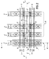
- the structure 1 is constructed in the form of a semiconductor integrated circuit incorporating thousands of cells 2. Shown diagramatically in Figure 1 is, however, just a portion of this circuit.
- the matrix provided by the structure 1 comprises a plurality of rows 3 and plurality of columns 4.
- Each row 3 includes a so-called word line WL and a corresponding control gate line CG.
- the columns 4 include the so-called bit lines of the matrix.
- bit lines BL are gathered into bytes 9, that is into groups of eight BL0,...,BL7 or sixteen adjacent lines which can be addressed simultaneously.
- bit line BL interconnects all the drain terminals of the common selection transistors 5 on a given column 4 of the matrix.
- Each selection transistor 5 is associated with and connected serially to a floating gate EEPROM cell 2.
- the cell 2 is of the type with a double level of polysilicon, and has a basic structure substantially of the FLOTOX type.
- the core of the memory cell 2 comprises a MOS transistor having a floating gate 12 where the electric charge is stored identifyings the two different, "written” or “erased", states of the cell.
- the floating gate is shown in Figure 2.
- the cell 2 would include a second, or control, gate 8, which is coupled capacitively to the floating gate 12 through an intervening dielectric layer called "interpoly". A voltage is transferred through said dielectric layer to the floating gate 12 from the control gate 8 during the write and/or erase phases of the cell 2.
- the control terminal of the control gate 8 is shared by all the cells 2 which form any one row 3 in the structure 1.
- Each row 3 of the matrix 1 is provided, to that aim, with a dedicated connection line CG interconnecting the gates 8.
- the structure 1 further comprises plural source addressing columns 7, each associated with a corresponding byte 9.
- Such columns 7 are also referred to as source addressing lines SL.
- the lines SL are each connected between each pair of adjacent bytes 9, that is to say, a column 7 is provided for each group of bit lines BL forming a byte 9.
- Each source addressing line SL connects the source terminals of a series of enable transistors A and B aligned on one column.
- the transistors denoted by A are provided at the crossover of each word line WL with the column 7, whereas the transistors denoted by B are provided at the crossover of each connection line CG connecting the control gates 8 to the column 7.
- the source terminals of all the transistors incorporated to the cells 2 of a single byte 9 are led to one and the same corresponding source line SL.
- the enable transistors A and B present in the source addressing line SL are not strictly necessary, although their provision has the advantage of minimizing noise, as explained hereinafter.
- the transistors A are intended for selecting the segment of that source line SL in the row 3 which would be addressed when accessing the memory structure. Each transistor A is driven from its respective word line WL.
- the transistors B are basically additional enable transistors. They are driven from their respective connection line CG and should be a high-voltage type in order to withstand the voltages that are applied during the erase phase.
- Each transistor B only represents a small increase in the series resistance of its respective source line SL. This resistance may be minimized, if desired, by appropriate selection of the transistor B length and width, or even removed altogether by shorting the transistors with an implant or a connecting bridge of polysilicon or metal.
- positive voltage pulses are usually employed for writing and erasing a given cell, which pulses are applied to the cell terminals such that a sufficient electric field is generated to induce a flow of current through the tunnel oxide layer.
- the memory structure of this invention provides for the use of a negative voltage, to be applied to the control gate 8 of each predetermined cell 2 during the write phase.
- the voltage at the control gate 8 is decoded by rows, as is that applied to the gate of the selection transistor 5.
- the voltage at the drain terminal is on the contrary decoded by columns, as is that at the source terminals of the line SL.
- the erase and read phases for the selected byte are run in a similar manner, with the difference that no negative voltages are applied here to the various terminals.
- the voltage on the word line during the erase phase may be zero.
- Table II shows the voltage values being applied to a byte which has not been selected but is present in the same row as the selected byte.
- Table III shows the voltage levels being applied to a byte which has not been selected but is present in the same column as the selected byte.
- V CG [V] WRITE float 5 6 -8 ERASE 0 float 6 16 READ 0 1 5 3
- V SOURCE [V] V DRAIN [V] WL select tr Unselected byte in the same row as the selected byte (same WL and CG.)
- V V CG [V] WRITE float float 6 -8 ERASE 5 float 6 16 READ float float 5 3 TABLE III Unselected byte in the same column as the selected byte. (Same decoding as the source)
- the polarizations applied to the various terminals are transferred in the same way as previously described; that is to say, the control gate decoding is carried out by rows, whereas the decoding of the drain and the source terminals is carried out by columns.
- the write phase is characterized by the use of a negative voltage at the control gate 8 and a positive voltage at the drain terminal of the cell 2; this allows generation of a sufficiently strong electric field to draw electrons from the floating gate 12.
- this operation does impose some noise on all the cells in one row 3.
- the negative voltage would also be applied to their control gate 8, which is in common with the line CG for all the cells in the same row 3.
- This noise may be difficult to suppress in the byte programming mode; but the effect of the noise can be minimized by appropriate adjustment of the values of the applied voltages.
- both the transistor A and the transistor B are conducting, and each cell 2 of the selected byte 9 is injected by electrons at the floating gate 12 through the channel region.
- the source lines SL of the unselected columns 7 are brought to a voltage of 5 Volts.
- the voltage is transferred to all the source segments related to each byte because the transistors A and B are conducting.
- the read phase is run in quite a conventional manner.
- the cells 2 in the matrix 1 are implemented in the MOS technology, starting with a P-doped semiconductor substrate 10, which has been formed with either N-type or P-type wells.
- the description to follow will begin with the step of photolithographically defining active area regions on the substrate 10.
- the common source regions 6 of cells 2 in the same byte 9 are structurally and electrically separate from those of the adjacent bytes, as brought out by Figure 5.
- field oxide 22 allows such regions 6 to be demarcated.
- the gate oxide is formed to different depths according to the different transistor types. For instance, a tunnel oxide 24 thickness of about 9 nm is preferred for the floating gate cells 2, while a thickness of about 20 nm would be appropriate for the selection transistors 5.
- the former may have a gate oxide 26 formed to either a thickness of 20 nm or 30 nm, that is, for a low or a high voltage, whilst the latter transistor B is to expressedly withstand high voltages and requires a thickness of about 30 nm for the gate oxide 16.
- steps such as by growing a first oxide layer of about 24 nm onto the surface of the substrate 10.
- This first layer would be masked with a resist and etched in those areas where the low-voltage oxide is to be grown. The resist is then removed, and a second oxide layer of about 18 nm grown.
- the depth of the first layer would also be increased.
- a subsequent masking step with a resist will enable the high- and low-voltage oxide 16, 26 areas to be protected, and the oxide layer etched away in the tunnel areas. Removal of the resist and subsequent growth of the tunnel dielectric 24 bring to completion the thickness of the low- and high-voltage oxides 16 and 26 as well.
- the process continues with the deposition, doping, and photolithographic definition of the first polycrystalline silicon (polysilicon) layer 20 for the floating gates 12 of the cells 2.
- a so-called interpoly dielectric layer 25 is formed over the first polysilicon layer 20.
- This interpoly layer 15 is removed, however, along the source addressing line SL shown in Figure 3 to later obtain standard transistors A and B having no floating gates.
- the other areas of the matrix 1 are protected with a photoresist during this operation.
- a second polysilicon layer 21 will allow the formation of the control gates 8 and those of the selection transistors 5, as well as the gates of the enable transistors A and B.
- the source and drain implantations are carried out for the cells 2, the selection transistors 5, and the active areas 15 of the transistors A and B, using at least one species of the N type.
- circuit structure of this invention as obtained with the process described hereinabove, does solve the technical problem and afford a number of advantages as follows.
- this solution allows the programming to be handled for each individual byte even where negative voltages are used during the write phase.
- the use of a negative voltage at the control gate 8 allows the voltage applied to the drain terminal to be lowered while maintaining, across the thin oxide, an electric field which is the equal of that provided in conventional cells. Thus, the deterioration of the thin tunnel oxide can be greatly reduced.
- the use of a negative voltage at the control gate 8 of the cells 2 during the write phase allows the voltage requirement across the tunnel oxide for obtaining a desired programming current to be distributed.
- the circuit of this invention can be integrated within a smaller area than a conventional cell of equal technology. Since the inventive cell works on the basis of a Fowler-Nordheim tunnel effect, and its intrinsic threshold may be selected close to zero, this structure would suit in particular low-voltage supply applications.
Abstract
Description
- This invention relates to a circuit structure for a memory cells matrix.
- More particularly, the invention relates to a matrix of EEPROM memory cells being of a type which comprises a cells matrix composed of plural rows and columns, each provided with a word line and a bit line respectively, wherein the bit lines are gathered into groups or bytes of adjacent lines which are simultaneously addressable, each of said cells incorporating a floating gate transistor connected serially to a selection transistor and having an additional control gate overlaying the floating gate.
- As is well known, EEPROM memory structures, while being non-volatile types, allow the information contained therein to be modified electrically at both the write and the erase phases of their operation. Furthermore, they distinguish themselves by the kind of their electric programming, which may take place in either the "page" mode or the "byte" mode.
- In the former mode, all the cells in one row of the matrix are addressed at one time. In the latter mode, one byte only is addressed of the several available in one row.
- It is also known that the state of any cell in the EEPROM memory can be altered by means of an electrons flow passing by tunnel effect through a thin layer of silicon oxide associated with the floating gate of the cell. The thin oxide region occupies a smaller area than the floating gate, whereat the electric charge is stored.
- There exist different types of EEPROM memory cells which are identifiable by the number of their polysilicon layers.
- In fact, there are cells with single, double, or treble layers of polysilicon. Most commonly employed are cells with two-level of polysilicon, known as FLOTOX cells; such cells are described, for instance, in an article "Oxide reliability criterion for the evaluation of endurance performance of electrically erasable programmable read-only memories", Journal App. Phys, 71, No. 9, 1992.
- Irrespective of the number of the polysilicon layers, for the write and erase phases of the cells, it is common practice to use positive voltages, applied to the diffusion underlying the tunnel region or the control gate. Such voltages vary between 8 and 18 Volts, in order to generate across the thin oxide an electric field which is sufficiently strong to positively trigger the tunnel effect.
- However, the use of such, comparatively high, positive voltages may result over time in the thin oxide layer being deteriorated, thereby damaging the cells and the whole memory structure beyond repair.
- One might think of obviating this problem by using negative voltages for programming, e.g. during the writing phase.
- It should not be overlooked, however, that with conventional type cells the byte mode programming is carried out by splitting the control gate into segments which are common to a single byte (e.g., eight or sixteen bits). The control gate is then selected by means of a column decoder external of the cells matrix, and is enabled by a select transistor shared by all the cells in one row.
- In this way, the programming will only be enabled in the selected byte.
- But the use of a negative voltage during this programming phase adduces some serious problems.
- As an example, a large integrated circuit area would have to be used for selecting a single byte, because each segment of the control gate requires the arrangement of a switch adapted to handle both the positive voltages and the negative voltages applied during the programming phase.
- The underlying technical problem of this invention is to provide a circuit structure for a matrix of memory cells, in particular of the EEPROM type, which has such structural and functional features as to improve the memory reliability, and extend its service life, while attenuating the deterioration of the tunnel oxide and obviating the programming problems when using negative voltages.
- A further object of the invention is to provide very high density integrated storage circuits which can occupy, for a given technology, a smaller circuit area than comparable circuits of conventional design. This would enable the manufacturing costs of high density storage circuits to be cut down drastically.
- The solutive idea on which this invention stands is one of splitting the so-called source line into regular segments shared by the cells of a single byte (having eight or sixteen bits, for example) and decoding such segments when a desired byte is programmed.
- On the grounds of this solutive idea, the technical problem is solved by a circuit structure of the kind outlined above and as defined in the characterizing part of
Claim 1. - The features and advantages of a circuit structure according to the invention will become apparent from the following detailed description of an embodiment thereof, given by way of example and not of limitation with reference to the accompanying drawings.
-
- Figure 1 is a diagramatic view of a circuit structure embodying this invention;
- Figure 2 is an enlarged schematic view from above of a semiconductor portion in which the inventive circuit structure is formed;
- Figure 3 is an enlarged schematic view in vertical section, taken along line III-III in Figure 2, of a semiconductor portion in which the circuit of this invention is formed;
- Figure 4 is an enlarged schematic view in vertical section, taken along line IV-IV in Figure 2, of a semiconductor portion in which the circuit of this invention is formed;
- Figure 5 is an enlarged schematic view in vertical section, taken along line V-V in Figure 2, of a semiconductor portion in which the circuit of this invention is formed.
- With reference to the drawing views, generally and schematically shown at 1 is a circuit structure for forming, in accordance with the invention, a matrix of
memory cells 2, in particular EEPROM memory cells. - The
structure 1 is constructed in the form of a semiconductor integrated circuit incorporating thousands ofcells 2. Shown diagramatically in Figure 1 is, however, just a portion of this circuit. - The matrix provided by the
structure 1 comprises a plurality ofrows 3 and plurality ofcolumns 4. Eachrow 3 includes a so-called word line WL and a corresponding control gate line CG. On the other hand, thecolumns 4 include the so-called bit lines of the matrix. - According to the memory size, the bit lines BL are gathered into bytes 9, that is into groups of eight BL₀,...,BL₇ or sixteen adjacent lines which can be addressed simultaneously.
- At the crossover of a word line WL with a bit line BL, there is a
selection transistor 5. In addition, a bit line BL interconnects all the drain terminals of thecommon selection transistors 5 on a givencolumn 4 of the matrix. - Each
selection transistor 5 is associated with and connected serially to a floatinggate EEPROM cell 2. - Specifically, the
cell 2 is of the type with a double level of polysilicon, and has a basic structure substantially of the FLOTOX type. The core of thememory cell 2 comprises a MOS transistor having afloating gate 12 where the electric charge is stored identifyings the two different, "written" or "erased", states of the cell. The floating gate is shown in Figure 2. - In general, the
cell 2 would include a second, or control,gate 8, which is coupled capacitively to thefloating gate 12 through an intervening dielectric layer called "interpoly". A voltage is transferred through said dielectric layer to thefloating gate 12 from thecontrol gate 8 during the write and/or erase phases of thecell 2. - The control terminal of the
control gate 8 is shared by all thecells 2 which form any onerow 3 in thestructure 1. Eachrow 3 of thematrix 1 is provided, to that aim, with a dedicated connection line CG interconnecting thegates 8. - Advantageously, according to the invention, the
structure 1 further comprises pluralsource addressing columns 7, each associated with a corresponding byte 9.Such columns 7 are also referred to as source addressing lines SL. - In the embodiment described herein by way of example, the lines SL are each connected between each pair of adjacent bytes 9, that is to say, a
column 7 is provided for each group of bit lines BL forming a byte 9. - Nothing forbids, however, to provide such source addressing lines SL between the bit lines BL.
- Each source addressing line SL connects the source terminals of a series of enable transistors A and B aligned on one column.
- The transistors denoted by A are provided at the crossover of each word line WL with the
column 7, whereas the transistors denoted by B are provided at the crossover of each connection line CG connecting thecontrol gates 8 to thecolumn 7. - Advantageously, according to the invention, the source terminals of all the transistors incorporated to the
cells 2 of a single byte 9 are led to one and the same corresponding source line SL. - In essence, it results as if the source line SL were split into segments, each in common with the
source regions 6 of thecells 2 which form a single byte 9. - From the practical embodiment illustrated by Figure 2, it can be appreciated that all the
cells 2 of a given byte 9 would have respective source regions formed in common with a corresponding one of the source lines SL. Additionally, the source regions of the symmetrical byte with the above - - i.e. the byte in thenext row 3 -- would also be in common. - The enable transistors A and B present in the source addressing line SL are not strictly necessary, although their provision has the advantage of minimizing noise, as explained hereinafter.
- The transistors A are intended for selecting the segment of that source line SL in the
row 3 which would be addressed when accessing the memory structure. Each transistor A is driven from its respective word line WL. - The transistors B are basically additional enable transistors. They are driven from their respective connection line CG and should be a high-voltage type in order to withstand the voltages that are applied during the erase phase.
- Each transistor B only represents a small increase in the series resistance of its respective source line SL. This resistance may be minimized, if desired, by appropriate selection of the transistor B length and width, or even removed altogether by shorting the transistors with an implant or a connecting bridge of polysilicon or metal.
- The method for programming the memory cell of this invention will now be described. In fact, the peculiar and innovative structure of this
cell 2 allows it to be programmed in quite a novel manner. - In conventional storage circuits, positive voltage pulses are usually employed for writing and erasing a given cell, which pulses are applied to the cell terminals such that a sufficient electric field is generated to induce a flow of current through the tunnel oxide layer.
- By contrast, the memory structure of this invention provides for the use of a negative voltage, to be applied to the
control gate 8 of eachpredetermined cell 2 during the write phase. - Specifically, during the write phase, to a selected byte is applied, at the various terminals, the voltages shown in the following Table I.
- Throughout the following Tables, there are shown -- for each write, erase, or read phase -- the voltage values on the source line SL, the bit line BL (drain contact), the word line WL (gate of the select transistor 5), and the
control gate 8. - The voltage at the
control gate 8 is decoded by rows, as is that applied to the gate of theselection transistor 5. The voltage at the drain terminal is on the contrary decoded by columns, as is that at the source terminals of the line SL. - The erase and read phases for the selected byte are run in a similar manner, with the difference that no negative voltages are applied here to the various terminals.
- If no enable transistors A and B are provided, the voltage on the word line during the erase phase may be zero.
- Table II, on the other hand, shows the voltage values being applied to a byte which has not been selected but is present in the same row as the selected byte.
- Likewise, Table III shows the voltage levels being applied to a byte which has not been selected but is present in the same column as the selected byte.
TABLE I Selected byte VSOURCE [V] VDRAIN [V] WLselect tr. [V] VCG [V] WRITE float 5 6 -8 ERASE 0 float 6 16 READ 0 1 5 3 TABLE II Unselected byte in the same row as the selected byte (same WL and CG.) VSOURCE [V] VDRAIN [V] WLselect tr. [V] VCG [V] WRITE float float 6 -8 ERASE 5 float 6 16 READ float float 5 3 TABLE III Unselected byte in the same column as the selected byte. (Same decoding as the source) VSOURCE [V] VDRAIN [V] WLselect tr. [V] VCG [V] WRITE float 5 0 0 ERASE 0 float 0 0 READ float float 0 0 TABLE IV Unselected byte in different row and column from the selected byte. VSOURCE [V] VDRAIN [V] WLselect tr. [V] VCG [V] WRITE float float 0 0 ERASE 5 float 0 0 READ float float 0 0 - In either cases, the polarizations applied to the various terminals are transferred in the same way as previously described; that is to say, the control gate decoding is carried out by rows, whereas the decoding of the drain and the source terminals is carried out by columns.
- Thus, it can be once more appreciated that the write phase is characterized by the use of a negative voltage at the
control gate 8 and a positive voltage at the drain terminal of thecell 2; this allows generation of a sufficiently strong electric field to draw electrons from the floatinggate 12. However, this operation does impose some noise on all the cells in onerow 3. - In fact, the negative voltage would also be applied to their
control gate 8, which is in common with the line CG for all the cells in thesame row 3. - This noise may be difficult to suppress in the byte programming mode; but the effect of the noise can be minimized by appropriate adjustment of the values of the applied voltages.
- During the erase phase, the voltage Vs=0 on the source column SL is taken from that column to the source terminals of the
cells 2 which belong to the selected byte 9. In fact, both the transistor A and the transistor B are conducting, and eachcell 2 of the selected byte 9 is injected by electrons at the floatinggate 12 through the channel region. - However, in order to prevent erasing of bytes not yet selected but placed in the
same row 3, the source lines SL of theunselected columns 7 are brought to a voltage of 5 Volts. Here again, the voltage is transferred to all the source segments related to each byte because the transistors A and B are conducting. - In this way, the electric field across tthe tunnel oxide will not be sufficiently strong to significantly trigger a Fowler-Nordheim conduction mechanism, and accordingly, the information stored in the cells of these unselected bytes is left unaltered.
- Additionally, all the bytes in rows other than the selected one will be unaffected by the erase and write operations because to their control gates no voltage are applied with a sufficiently high (whether positive or negative) value. It matters to observe that no noise from the comparatively low voltage applied to the source columns SL during the erase phase would appear on the bytes of the unselected rows, because the transistor A is cut off during this phase and no voltage is transferred to the source terminals, thereby allowing them to float.
- The read phase is run in quite a conventional manner.
- With reference in particular to the examples of Figures 2 to 5, the steps of the manufacturing method which lead to the formation of a semiconductor integrated device incorporating the circuit structure of this invention will now be described.
- Specifically, the process steps will be described herein below leading to a circuit also incorporating the transistors A and B for the source addressing line SL.
- The
cells 2 in thematrix 1 are implemented in the MOS technology, starting with a P-doped semiconductor substrate 10, which has been formed with either N-type or P-type wells. - Thus, the description to follow will begin with the step of photolithographically defining active area regions on the substrate 10. Among these active areas, the
common source regions 6 ofcells 2 in the same byte 9 are structurally and electrically separate from those of the adjacent bytes, as brought out by Figure 5. - The growth of
field oxide 22 allowssuch regions 6 to be demarcated. - Then, the gate oxide is formed to different depths according to the different transistor types. For instance, a
tunnel oxide 24 thickness of about 9 nm is preferred for the floatinggate cells 2, while a thickness of about 20 nm would be appropriate for theselection transistors 5. - As for the transistors A and B of the source addressing line SL, the former may have a
gate oxide 26 formed to either a thickness of 20 nm or 30 nm, that is, for a low or a high voltage, whilst the latter transistor B is to expressedly withstand high voltages and requires a thickness of about 30 nm for thegate oxide 16. - In order to provide thicknesses so markedly different from one another, one can proceed in steps, such as by growing a first oxide layer of about 24 nm onto the surface of the substrate 10.
- This first layer would be masked with a resist and etched in those areas where the low-voltage oxide is to be grown. The resist is then removed, and a second oxide layer of about 18 nm grown.
- During this second growth, the depth of the first layer would also be increased.
- A subsequent masking step with a resist will enable the high- and low-
voltage oxide tunnel dielectric 24 bring to completion the thickness of the low- and high-voltage oxides - Nothing forbids, of course, that a different procedure be used to provide such different oxide thickness. The process continues with the deposition, doping, and photolithographic definition of the first polycrystalline silicon (polysilicon)
layer 20 for the floatinggates 12 of thecells 2. A so-calledinterpoly dielectric layer 25 is formed over thefirst polysilicon layer 20. - This
interpoly layer 15 is removed, however, along the source addressing line SL shown in Figure 3 to later obtain standard transistors A and B having no floating gates. The other areas of thematrix 1 are protected with a photoresist during this operation. - Moreover, the deposition and doping of a
second polysilicon layer 21 will allow the formation of thecontrol gates 8 and those of theselection transistors 5, as well as the gates of the enable transistors A and B. - Thereafter, the source and drain implantations are carried out for the
cells 2, theselection transistors 5, and theactive areas 15 of the transistors A and B, using at least one species of the N type. - The process is completed by subsequent steps, known per se, which will provide:
- so-called
spacers 19; - N- and P-channel transistors for the circuitry associated with the
matrix 1; and - an intervening
dielectric 17 and a terminatingmetallization layer 18. - On the whole, the process just described has a major advantage in that it can be completed using no additional steps with respect to conventional methods.
- The circuit structure of this invention, as obtained with the process described hereinabove, does solve the technical problem and afford a number of advantages as follows.
- First, this solution allows the programming to be handled for each individual byte even where negative voltages are used during the write phase.
- The use of a negative voltage at the
control gate 8 allows the voltage applied to the drain terminal to be lowered while maintaining, across the thin oxide, an electric field which is the equal of that provided in conventional cells. Thus, the deterioration of the thin tunnel oxide can be greatly reduced. - In addition, the use of a negative voltage at the
control gate 8 of thecells 2 during the write phase, allows the voltage requirement across the tunnel oxide for obtaining a desired programming current to be distributed. - The circuit of this invention can be integrated within a smaller area than a conventional cell of equal technology. Since the inventive cell works on the basis of a Fowler-Nordheim tunnel effect, and its intrinsic threshold may be selected close to zero, this structure would suit in particular low-voltage supply applications.
- Understandably the memory cell herein described and illustrated may be altered and modified in many ways without departing from the invention scope as defined in the appended claims.
Claims (12)
- A circuit structure for a matrix of EEPROM memory cells, being of a type which comprises a matrix of cells (2) including plural rows (3) and columns (4), with each row (3) being provided with a word line (WL) and a control gate line (CG) and each column (4) having a bit line (BL), said bit lines (BL) being gathered into groups or bytes (9) of simultaneously addressable adjacent lines, and the matrix cells (2) incorporating each a floating gate transistor (12) which is coupled to a control gate (8) connected to the control gate line (CG) and is connected serially to a selection transistor (5), characterized in that:
the cells (2) of each individual byte (9) share their respective source areas (6), such areas being structurally independent for each byte (9) and being led to a corresponding source addressing line (SL) extending along a matrix column (7). - A circuit structure according to Claim 1, characterized in that said source addressing line (SL) is split substantially into segments shared by the cells (2) of each individual byte (9).
- A circuit structure according to Claim 1, characterized in that said source addressing line is decoded when selecting a desired byte (9).
- A circuit structure according to Claim 2, characterized in that each segment (6) is individually addressable, and is decoded when accessing or programming the desired byte (9).
- A circuit structure according to Claim 1, characterized in that said source addressing line (SL) comprises at least one enable transistor (A) connected to the source regions (6) of the cells (2) of one and the same byte (9).
- A circuit structure according to Claim 5, characterized in that said enable transistor (A) is provided at the crossover of each word line (WL) with the source line (SL).
- A circuit structure according to Claim 1, characterized in that said source addressing line (SL) comprises at least a pair of enable transistors (A,B) connected to the source regions (6) of one and the same byte (9).
- A circuit structure according to Claim 7, characterized in that the former (A) of said enable transistors (A,B) is provided at the crossover of each word line (WL) with the source addressing line (SL).
- A circuit structure according to Claim 7, characterized in that the latter (B) of the enable transistors is provided at the crossover of each control gate (8) line (CG) with the source addressing line (SL).
- A method for making, in MOS technology, a matrix (1) of memory cells (2) of a type formed, in MOS technology, on a semiconductor substrate (10), the cells (2) comprising floating gate (12) transistors having active source (6) and drain areas and being each connected serially to a respective selection transistor (5), characterized in that it provides for the formation of plural addressing lines (SL) for said active source areas (6) extending along columns (7) of the matrix (1) and each including enable transistors (A,B) formed concurrently with the floating gate transistors and the selection transistors (5).
- A method according to Claim 9, characterized in that the active source areas (6) of the transistors incorporated into the cells (2) of a given byte (9) are formed in common with one and the same corresponding source addressing line (SL).
- A circuit structure according to Claim 1, characterized in that the source terminals of the transistors incorporated into the cells (2) of a predetermined byte (9) are connected to one and the same corresponding source addressing line (SL).
Priority Applications (5)
| Application Number | Priority Date | Filing Date | Title |
|---|---|---|---|
| EP93830339A EP0637035B1 (en) | 1993-07-29 | 1993-07-29 | Circuit structure for a memory matrix and corresponding manufacturing method |
| DE69305986T DE69305986T2 (en) | 1993-07-29 | 1993-07-29 | Circuit structure for memory matrix and corresponding manufacturing processes |
| JP6197977A JPH07147390A (en) | 1993-07-29 | 1994-07-29 | Circuit structure for memory cell matrix and its manufacture |
| US08/474,735 US5597750A (en) | 1993-07-29 | 1995-06-07 | Method of manufacturing a matrix of memory cells having control gates |
| US08/688,233 US5677871A (en) | 1993-07-29 | 1996-07-29 | Circuit structure for a memory matrix and corresponding manufacturing method |
Applications Claiming Priority (1)
| Application Number | Priority Date | Filing Date | Title |
|---|---|---|---|
| EP93830339A EP0637035B1 (en) | 1993-07-29 | 1993-07-29 | Circuit structure for a memory matrix and corresponding manufacturing method |
Publications (2)
| Publication Number | Publication Date |
|---|---|
| EP0637035A1 true EP0637035A1 (en) | 1995-02-01 |
| EP0637035B1 EP0637035B1 (en) | 1996-11-13 |
Family
ID=8215209
Family Applications (1)
| Application Number | Title | Priority Date | Filing Date |
|---|---|---|---|
| EP93830339A Expired - Lifetime EP0637035B1 (en) | 1993-07-29 | 1993-07-29 | Circuit structure for a memory matrix and corresponding manufacturing method |
Country Status (4)
| Country | Link |
|---|---|
| US (2) | US5597750A (en) |
| EP (1) | EP0637035B1 (en) |
| JP (1) | JPH07147390A (en) |
| DE (1) | DE69305986T2 (en) |
Cited By (8)
| Publication number | Priority date | Publication date | Assignee | Title |
|---|---|---|---|---|
| EP0750313A1 (en) * | 1995-06-21 | 1996-12-27 | STMicroelectronics S.A. | EEPROM memory, programmed and erased by Fowler-Nordheim effect |
| WO1997021225A2 (en) * | 1995-12-06 | 1997-06-12 | Siemens Aktiengesellschaft | Read-only memory and method of commanding same |
| WO1997021224A2 (en) * | 1995-12-06 | 1997-06-12 | Siemens Aktiengesellschaft | Eeprom and method of controlling same |
| EP0811986A1 (en) * | 1996-06-05 | 1997-12-10 | STMicroelectronics S.r.l. | Page-mode memory device with multiple-level memory cells |
| US5963478A (en) * | 1995-12-06 | 1999-10-05 | Siemens Aktiengesellschaft | EEPROM and method of driving the same |
| CN1050227C (en) * | 1995-06-09 | 2000-03-08 | 现代电子产业株式会社 | Memory integrated circuit and methods for manufacturing the same |
| CN1114228C (en) * | 1996-06-14 | 2003-07-09 | 冲电气工业株式会社 | Semiconductor memory and mfg. method therefor |
| US8320191B2 (en) | 2007-08-30 | 2012-11-27 | Infineon Technologies Ag | Memory cell arrangement, method for controlling a memory cell, memory array and electronic device |
Families Citing this family (10)
| Publication number | Priority date | Publication date | Assignee | Title |
|---|---|---|---|---|
| US6291851B1 (en) * | 1995-07-21 | 2001-09-18 | Rohm Co., Ltd. | Semiconductor device having oxide layers formed with different thicknesses |
| US5861333A (en) * | 1996-10-25 | 1999-01-19 | United Microelectonics Corp. | Method of tunnel window process for EEPROM cell technology |
| US5763307A (en) * | 1996-11-08 | 1998-06-09 | Advanced Micro Devices, Inc. | Block select transistor and method of fabrication |
| USRE37419E1 (en) * | 1997-06-05 | 2001-10-23 | Aplus Flash Technology Inc. | Flash memory array and decoding architecture |
| US6071778A (en) * | 1998-02-20 | 2000-06-06 | Stmicroelectronics S.R.L. | Memory device with a memory cell array in triple well, and related manufacturing process |
| IT1301880B1 (en) | 1998-07-30 | 2000-07-07 | St Microelectronics Srl | ELECTRONIC MEMORY CIRCUIT AND CORRESPONDING MANUFACTURING METHOD |
| JP2002016238A (en) * | 2000-06-29 | 2002-01-18 | Mitsubishi Electric Corp | Semiconductor device |
| US7483505B2 (en) * | 2001-04-27 | 2009-01-27 | The Directv Group, Inc. | Unblind equalizer architecture for digital communication systems |
| US7388251B2 (en) * | 2004-08-11 | 2008-06-17 | Micron Technology, Inc. | Non-planar flash memory array with shielded floating gates on silicon mesas |
| EP1727152B1 (en) * | 2005-05-18 | 2008-12-24 | STMicroelectronics SA | EEPROM memory architecture |
Citations (4)
| Publication number | Priority date | Publication date | Assignee | Title |
|---|---|---|---|---|
| EP0182198A2 (en) * | 1984-11-21 | 1986-05-28 | Rohm Corporation | Single transistor electrically programmable device and method |
| JPS6260266A (en) * | 1985-09-10 | 1987-03-16 | Toshiba Corp | Non-volatile semiconductor memory device |
| WO1989006429A1 (en) * | 1987-12-28 | 1989-07-13 | Elite Semiconductor & Systems International, Inc. | Rom cell and array configuration |
| EP0326465A1 (en) * | 1988-01-26 | 1989-08-02 | STMicroelectronics S.A. | Floating-gate EEPROM memory with a transistor for source line selection |
Family Cites Families (12)
| Publication number | Priority date | Publication date | Assignee | Title |
|---|---|---|---|---|
| JPS5974677A (en) * | 1982-10-22 | 1984-04-27 | Ricoh Co Ltd | Semiconductor device and manufacture thereof |
| FR2622038B1 (en) * | 1987-10-19 | 1990-01-19 | Thomson Semiconducteurs | METHOD FOR PROGRAMMING MEMORY CELLS OF A MEMORY AND CIRCUIT FOR IMPLEMENTING SAID METHOD |
| JPH01137496A (en) * | 1987-11-20 | 1989-05-30 | Mitsubishi Electric Corp | Non-volatile semiconductor storage |
| US4999812A (en) * | 1988-11-23 | 1991-03-12 | National Semiconductor Corp. | Architecture for a flash erase EEPROM memory |
| US5081054A (en) * | 1989-04-03 | 1992-01-14 | Atmel Corporation | Fabrication process for programmable and erasable MOS memory device |
| KR930000869B1 (en) * | 1989-11-30 | 1993-02-08 | 삼성전자 주식회사 | Flash type eeprom device which is able to eliminate page |
| US5188976A (en) * | 1990-07-13 | 1993-02-23 | Hitachi, Ltd. | Manufacturing method of non-volatile semiconductor memory device |
| KR940004404B1 (en) * | 1990-11-30 | 1994-05-25 | 삼성전자 주식회사 | Nonvolatile semiconductor memory device |
| US5363330A (en) * | 1991-01-28 | 1994-11-08 | Mitsubishi Denki Kabushiki Kaisha | Non-volatile semiconductor memory device incorporating data latch and address counter for page mode programming |
| US5317535A (en) * | 1992-06-19 | 1994-05-31 | Intel Corporation | Gate/source disturb protection for sixteen-bit flash EEPROM memory arrays |
| US5339279A (en) * | 1993-05-07 | 1994-08-16 | Motorola, Inc. | Block erasable flash EEPROM apparatus and method thereof |
| US5365484A (en) * | 1993-08-23 | 1994-11-15 | Advanced Micro Devices, Inc. | Independent array grounds for flash EEPROM array with paged erase architechture |
-
1993
- 1993-07-29 DE DE69305986T patent/DE69305986T2/en not_active Expired - Fee Related
- 1993-07-29 EP EP93830339A patent/EP0637035B1/en not_active Expired - Lifetime
-
1994
- 1994-07-29 JP JP6197977A patent/JPH07147390A/en active Pending
-
1995
- 1995-06-07 US US08/474,735 patent/US5597750A/en not_active Expired - Lifetime
-
1996
- 1996-07-29 US US08/688,233 patent/US5677871A/en not_active Expired - Lifetime
Patent Citations (4)
| Publication number | Priority date | Publication date | Assignee | Title |
|---|---|---|---|---|
| EP0182198A2 (en) * | 1984-11-21 | 1986-05-28 | Rohm Corporation | Single transistor electrically programmable device and method |
| JPS6260266A (en) * | 1985-09-10 | 1987-03-16 | Toshiba Corp | Non-volatile semiconductor memory device |
| WO1989006429A1 (en) * | 1987-12-28 | 1989-07-13 | Elite Semiconductor & Systems International, Inc. | Rom cell and array configuration |
| EP0326465A1 (en) * | 1988-01-26 | 1989-08-02 | STMicroelectronics S.A. | Floating-gate EEPROM memory with a transistor for source line selection |
Non-Patent Citations (2)
| Title |
|---|
| GIORA YARON ET AL: "A 16K E2PROM employing new array architecture and designed-in reliability features", IEEE JOURNAL OF SOLID-STATE CIRCUITS., vol. 17, no. 5, October 1982 (1982-10-01), NEW YORK US, pages 833 - 840 * |
| PATENT ABSTRACTS OF JAPAN vol. 11, no. 249 (E - 532)<2696> 13 August 1987 (1987-08-13) * |
Cited By (18)
| Publication number | Priority date | Publication date | Assignee | Title |
|---|---|---|---|---|
| US6051461A (en) * | 1995-06-09 | 2000-04-18 | Hyundai Electronics Industries Co., Ltd. | Memory integrated circuit and methods for manufacturing the same |
| CN1050227C (en) * | 1995-06-09 | 2000-03-08 | 现代电子产业株式会社 | Memory integrated circuit and methods for manufacturing the same |
| US6011717A (en) * | 1995-06-21 | 2000-01-04 | Stmicroelectronics S.A. | EEPROM memory programmable and erasable by Fowler-Nordheim effect |
| FR2735896A1 (en) * | 1995-06-21 | 1996-12-27 | Sgs Thomson Microelectronics | PROGRAMMABLE AND ERASABLE EEPROM MEMORY BY FOWLER-NORDHEIM EFFECT |
| EP0750313A1 (en) * | 1995-06-21 | 1996-12-27 | STMicroelectronics S.A. | EEPROM memory, programmed and erased by Fowler-Nordheim effect |
| WO1997021224A3 (en) * | 1995-12-06 | 1997-08-07 | Siemens Ag | Eeprom and method of controlling same |
| US5963478A (en) * | 1995-12-06 | 1999-10-05 | Siemens Aktiengesellschaft | EEPROM and method of driving the same |
| WO1997021225A3 (en) * | 1995-12-06 | 1997-08-14 | Siemens Ag | Read-only memory and method of commanding same |
| WO1997021224A2 (en) * | 1995-12-06 | 1997-06-12 | Siemens Aktiengesellschaft | Eeprom and method of controlling same |
| WO1997021225A2 (en) * | 1995-12-06 | 1997-06-12 | Siemens Aktiengesellschaft | Read-only memory and method of commanding same |
| US6166952A (en) * | 1995-12-06 | 2000-12-26 | Infineon Technologies Ag | Read-only memory having specially output circuits and word line connected to a group of memory cells |
| EP1191541A2 (en) * | 1995-12-06 | 2002-03-27 | Infineon Technologies AG | EEPROM and method of controlling same |
| EP1191541A3 (en) * | 1995-12-06 | 2002-08-14 | Infineon Technologies AG | EEPROM and method of controlling same |
| USRE41734E1 (en) | 1995-12-06 | 2010-09-21 | Infineon Technologies Ag | Read-only memory having specially output circuits and word line connected to a group of memory cells |
| EP0811986A1 (en) * | 1996-06-05 | 1997-12-10 | STMicroelectronics S.r.l. | Page-mode memory device with multiple-level memory cells |
| CN1114228C (en) * | 1996-06-14 | 2003-07-09 | 冲电气工业株式会社 | Semiconductor memory and mfg. method therefor |
| US8320191B2 (en) | 2007-08-30 | 2012-11-27 | Infineon Technologies Ag | Memory cell arrangement, method for controlling a memory cell, memory array and electronic device |
| US9030877B2 (en) | 2007-08-30 | 2015-05-12 | Infineon Technologies Ag | Memory cell arrangement, method for controlling a memory cell, memory array and electronic device |
Also Published As
| Publication number | Publication date |
|---|---|
| DE69305986T2 (en) | 1997-03-06 |
| JPH07147390A (en) | 1995-06-06 |
| US5677871A (en) | 1997-10-14 |
| US5597750A (en) | 1997-01-28 |
| EP0637035B1 (en) | 1996-11-13 |
| DE69305986D1 (en) | 1996-12-19 |
Similar Documents
| Publication | Publication Date | Title |
|---|---|---|
| US5422844A (en) | Memory array with field oxide islands eliminated and method | |
| EP0637035B1 (en) | Circuit structure for a memory matrix and corresponding manufacturing method | |
| JP3245054B2 (en) | Manufacturing method of memory array, programming method and memory array | |
| US7372736B2 (en) | Monolithic, combo nonvolatile memory allowing byte, page and block write with no disturb and divided-well in the cell array using a unified cell structure and technology with a new scheme of decoder and layout | |
| US6261907B1 (en) | Method of forming a flash EEPROM device by employing polysilicon sidewall spacer as an erase gate | |
| EP0555039B1 (en) | Alternate source virtual ground flash EPROM cell array | |
| USRE39697E1 (en) | Method of making floating-gate memory-cell array with digital logic transistors | |
| US5862082A (en) | Two transistor flash EEprom cell and method of operating same | |
| KR101113944B1 (en) | A method for programming and erasing an array of nmos eeprom cells that minimize bit disturbances and voltage withstand requirements for the memory array and supporting circuits | |
| EP0488804B1 (en) | Non-volatile semiconductor memory device | |
| EP2267775B1 (en) | Independently programmable memory segments in isolated n-wells within a pmos eeprom array | |
| KR100379553B1 (en) | A array of flash memory cell and method for programming of data thereby and method for erased of data thereby | |
| US6888753B2 (en) | Memory cell array comprising individually addressable memory cells and method of making the same | |
| EP0053075B1 (en) | Nonvolatile memory | |
| EP0466051B1 (en) | Non-volatile progammable read only memory device having memory cells each implemented by a memory transistor and a switching transistor coupled in parallel and method of memorizing a data bit | |
| US6839278B1 (en) | Highly-integrated flash memory and mask ROM array architecture | |
| US5394357A (en) | Non-volatile semiconductor memory device | |
| US5280187A (en) | Electrically programmable and erasable semiconductor memory and method of operating same | |
| US6525959B1 (en) | NOR array with buried trench source line | |
| EP0647947A2 (en) | Low voltage flash EEPROM X-cell using Fowler-Nordheim tunneling | |
| JP3185891B2 (en) | Nonvolatile semiconductor memory device and method of manufacturing the same |
Legal Events
| Date | Code | Title | Description |
|---|---|---|---|
| PUAI | Public reference made under article 153(3) epc to a published international application that has entered the european phase |
Free format text: ORIGINAL CODE: 0009012 |
|
| AK | Designated contracting states |
Kind code of ref document: A1 Designated state(s): DE FR GB IT |
|
| 17P | Request for examination filed |
Effective date: 19950724 |
|
| 17Q | First examination report despatched |
Effective date: 19950918 |
|
| GRAG | Despatch of communication of intention to grant |
Free format text: ORIGINAL CODE: EPIDOS AGRA |
|
| GRAG | Despatch of communication of intention to grant |
Free format text: ORIGINAL CODE: EPIDOS AGRA |
|
| GRAH | Despatch of communication of intention to grant a patent |
Free format text: ORIGINAL CODE: EPIDOS IGRA |
|
| GRAH | Despatch of communication of intention to grant a patent |
Free format text: ORIGINAL CODE: EPIDOS IGRA |
|
| GRAA | (expected) grant |
Free format text: ORIGINAL CODE: 0009210 |
|
| AK | Designated contracting states |
Kind code of ref document: B1 Designated state(s): DE FR GB IT |
|
| ITF | It: translation for a ep patent filed |
Owner name: PORTA CHECCACCI E BOTTI S.R.L. |
|
| REF | Corresponds to: |
Ref document number: 69305986 Country of ref document: DE Date of ref document: 19961219 |
|
| ET | Fr: translation filed | ||
| PLBE | No opposition filed within time limit |
Free format text: ORIGINAL CODE: 0009261 |
|
| STAA | Information on the status of an ep patent application or granted ep patent |
Free format text: STATUS: NO OPPOSITION FILED WITHIN TIME LIMIT |
|
| 26N | No opposition filed | ||
| REG | Reference to a national code |
Ref country code: GB Ref legal event code: IF02 |
|
| PGFP | Annual fee paid to national office [announced via postgrant information from national office to epo] |
Ref country code: DE Payment date: 20020807 Year of fee payment: 10 |
|
| PG25 | Lapsed in a contracting state [announced via postgrant information from national office to epo] |
Ref country code: DE Free format text: LAPSE BECAUSE OF NON-PAYMENT OF DUE FEES Effective date: 20040203 |
|
| PGFP | Annual fee paid to national office [announced via postgrant information from national office to epo] |
Ref country code: FR Payment date: 20040708 Year of fee payment: 12 |
|
| PGFP | Annual fee paid to national office [announced via postgrant information from national office to epo] |
Ref country code: GB Payment date: 20040728 Year of fee payment: 12 |
|
| PG25 | Lapsed in a contracting state [announced via postgrant information from national office to epo] |
Ref country code: IT Free format text: LAPSE BECAUSE OF NON-PAYMENT OF DUE FEES;WARNING: LAPSES OF ITALIAN PATENTS WITH EFFECTIVE DATE BEFORE 2007 MAY HAVE OCCURRED AT ANY TIME BEFORE 2007. THE CORRECT EFFECTIVE DATE MAY BE DIFFERENT FROM THE ONE RECORDED. Effective date: 20050729 Ref country code: GB Free format text: LAPSE BECAUSE OF NON-PAYMENT OF DUE FEES Effective date: 20050729 |
|
| GBPC | Gb: european patent ceased through non-payment of renewal fee |
Effective date: 20050729 |
|
| PG25 | Lapsed in a contracting state [announced via postgrant information from national office to epo] |
Ref country code: FR Free format text: LAPSE BECAUSE OF NON-PAYMENT OF DUE FEES Effective date: 20060331 |
|
| REG | Reference to a national code |
Ref country code: FR Ref legal event code: ST Effective date: 20060331 |