EP0638931A2 - Multi-chip module - Google Patents
Multi-chip module Download PDFInfo
- Publication number
- EP0638931A2 EP0638931A2 EP19940400928 EP94400928A EP0638931A2 EP 0638931 A2 EP0638931 A2 EP 0638931A2 EP 19940400928 EP19940400928 EP 19940400928 EP 94400928 A EP94400928 A EP 94400928A EP 0638931 A2 EP0638931 A2 EP 0638931A2
- Authority
- EP
- European Patent Office
- Prior art keywords
- chip module
- thin
- film
- circuit board
- board
- Prior art date
- Legal status (The legal status is an assumption and is not a legal conclusion. Google has not performed a legal analysis and makes no representation as to the accuracy of the status listed.)
- Granted
Links
Images


Classifications
-
- H—ELECTRICITY
- H01—ELECTRIC ELEMENTS
- H01L—SEMICONDUCTOR DEVICES NOT COVERED BY CLASS H10
- H01L25/00—Assemblies consisting of a plurality of individual semiconductor or other solid state devices ; Multistep manufacturing processes thereof
- H01L25/03—Assemblies consisting of a plurality of individual semiconductor or other solid state devices ; Multistep manufacturing processes thereof all the devices being of a type provided for in the same subgroup of groups H01L27/00 - H01L33/00, or in a single subclass of H10K, H10N, e.g. assemblies of rectifier diodes
- H01L25/04—Assemblies consisting of a plurality of individual semiconductor or other solid state devices ; Multistep manufacturing processes thereof all the devices being of a type provided for in the same subgroup of groups H01L27/00 - H01L33/00, or in a single subclass of H10K, H10N, e.g. assemblies of rectifier diodes the devices not having separate containers
- H01L25/065—Assemblies consisting of a plurality of individual semiconductor or other solid state devices ; Multistep manufacturing processes thereof all the devices being of a type provided for in the same subgroup of groups H01L27/00 - H01L33/00, or in a single subclass of H10K, H10N, e.g. assemblies of rectifier diodes the devices not having separate containers the devices being of a type provided for in group H01L27/00
- H01L25/0657—Stacked arrangements of devices
-
- H—ELECTRICITY
- H01—ELECTRIC ELEMENTS
- H01L—SEMICONDUCTOR DEVICES NOT COVERED BY CLASS H10
- H01L23/00—Details of semiconductor or other solid state devices
- H01L23/48—Arrangements for conducting electric current to or from the solid state body in operation, e.g. leads, terminal arrangements ; Selection of materials therefor
- H01L23/488—Arrangements for conducting electric current to or from the solid state body in operation, e.g. leads, terminal arrangements ; Selection of materials therefor consisting of soldered or bonded constructions
- H01L23/498—Leads, i.e. metallisations or lead-frames on insulating substrates, e.g. chip carriers
- H01L23/49811—Additional leads joined to the metallisation on the insulating substrate, e.g. pins, bumps, wires, flat leads
-
- H—ELECTRICITY
- H05—ELECTRIC TECHNIQUES NOT OTHERWISE PROVIDED FOR
- H05K—PRINTED CIRCUITS; CASINGS OR CONSTRUCTIONAL DETAILS OF ELECTRIC APPARATUS; MANUFACTURE OF ASSEMBLAGES OF ELECTRICAL COMPONENTS
- H05K1/00—Printed circuits
- H05K1/02—Details
- H05K1/14—Structural association of two or more printed circuits
- H05K1/141—One or more single auxiliary printed circuits mounted on a main printed circuit, e.g. modules, adapters
-
- H—ELECTRICITY
- H01—ELECTRIC ELEMENTS
- H01L—SEMICONDUCTOR DEVICES NOT COVERED BY CLASS H10
- H01L2224/00—Indexing scheme for arrangements for connecting or disconnecting semiconductor or solid-state bodies and methods related thereto as covered by H01L24/00
- H01L2224/01—Means for bonding being attached to, or being formed on, the surface to be connected, e.g. chip-to-package, die-attach, "first-level" interconnects; Manufacturing methods related thereto
- H01L2224/10—Bump connectors; Manufacturing methods related thereto
- H01L2224/15—Structure, shape, material or disposition of the bump connectors after the connecting process
- H01L2224/16—Structure, shape, material or disposition of the bump connectors after the connecting process of an individual bump connector
-
- H—ELECTRICITY
- H01—ELECTRIC ELEMENTS
- H01L—SEMICONDUCTOR DEVICES NOT COVERED BY CLASS H10
- H01L2224/00—Indexing scheme for arrangements for connecting or disconnecting semiconductor or solid-state bodies and methods related thereto as covered by H01L24/00
- H01L2224/01—Means for bonding being attached to, or being formed on, the surface to be connected, e.g. chip-to-package, die-attach, "first-level" interconnects; Manufacturing methods related thereto
- H01L2224/42—Wire connectors; Manufacturing methods related thereto
- H01L2224/47—Structure, shape, material or disposition of the wire connectors after the connecting process
- H01L2224/48—Structure, shape, material or disposition of the wire connectors after the connecting process of an individual wire connector
- H01L2224/481—Disposition
- H01L2224/48151—Connecting between a semiconductor or solid-state body and an item not being a semiconductor or solid-state body, e.g. chip-to-substrate, chip-to-passive
- H01L2224/48221—Connecting between a semiconductor or solid-state body and an item not being a semiconductor or solid-state body, e.g. chip-to-substrate, chip-to-passive the body and the item being stacked
- H01L2224/48225—Connecting between a semiconductor or solid-state body and an item not being a semiconductor or solid-state body, e.g. chip-to-substrate, chip-to-passive the body and the item being stacked the item being non-metallic, e.g. insulating substrate with or without metallisation
- H01L2224/48227—Connecting between a semiconductor or solid-state body and an item not being a semiconductor or solid-state body, e.g. chip-to-substrate, chip-to-passive the body and the item being stacked the item being non-metallic, e.g. insulating substrate with or without metallisation connecting the wire to a bond pad of the item
-
- H—ELECTRICITY
- H01—ELECTRIC ELEMENTS
- H01L—SEMICONDUCTOR DEVICES NOT COVERED BY CLASS H10
- H01L2225/00—Details relating to assemblies covered by the group H01L25/00 but not provided for in its subgroups
- H01L2225/03—All the devices being of a type provided for in the same subgroup of groups H01L27/00 - H01L33/648 and H10K99/00
- H01L2225/04—All the devices being of a type provided for in the same subgroup of groups H01L27/00 - H01L33/648 and H10K99/00 the devices not having separate containers
- H01L2225/065—All the devices being of a type provided for in the same subgroup of groups H01L27/00 - H01L33/648 and H10K99/00 the devices not having separate containers the devices being of a type provided for in group H01L27/00
- H01L2225/06503—Stacked arrangements of devices
- H01L2225/0651—Wire or wire-like electrical connections from device to substrate
-
- H—ELECTRICITY
- H01—ELECTRIC ELEMENTS
- H01L—SEMICONDUCTOR DEVICES NOT COVERED BY CLASS H10
- H01L2225/00—Details relating to assemblies covered by the group H01L25/00 but not provided for in its subgroups
- H01L2225/03—All the devices being of a type provided for in the same subgroup of groups H01L27/00 - H01L33/648 and H10K99/00
- H01L2225/04—All the devices being of a type provided for in the same subgroup of groups H01L27/00 - H01L33/648 and H10K99/00 the devices not having separate containers
- H01L2225/065—All the devices being of a type provided for in the same subgroup of groups H01L27/00 - H01L33/648 and H10K99/00 the devices not having separate containers the devices being of a type provided for in group H01L27/00
- H01L2225/06503—Stacked arrangements of devices
- H01L2225/06555—Geometry of the stack, e.g. form of the devices, geometry to facilitate stacking
-
- H—ELECTRICITY
- H01—ELECTRIC ELEMENTS
- H01L—SEMICONDUCTOR DEVICES NOT COVERED BY CLASS H10
- H01L2225/00—Details relating to assemblies covered by the group H01L25/00 but not provided for in its subgroups
- H01L2225/03—All the devices being of a type provided for in the same subgroup of groups H01L27/00 - H01L33/648 and H10K99/00
- H01L2225/04—All the devices being of a type provided for in the same subgroup of groups H01L27/00 - H01L33/648 and H10K99/00 the devices not having separate containers
- H01L2225/065—All the devices being of a type provided for in the same subgroup of groups H01L27/00 - H01L33/648 and H10K99/00 the devices not having separate containers the devices being of a type provided for in group H01L27/00
- H01L2225/06503—Stacked arrangements of devices
- H01L2225/06572—Auxiliary carrier between devices, the carrier having an electrical connection structure
-
- H—ELECTRICITY
- H01—ELECTRIC ELEMENTS
- H01L—SEMICONDUCTOR DEVICES NOT COVERED BY CLASS H10
- H01L2225/00—Details relating to assemblies covered by the group H01L25/00 but not provided for in its subgroups
- H01L2225/03—All the devices being of a type provided for in the same subgroup of groups H01L27/00 - H01L33/648 and H10K99/00
- H01L2225/04—All the devices being of a type provided for in the same subgroup of groups H01L27/00 - H01L33/648 and H10K99/00 the devices not having separate containers
- H01L2225/065—All the devices being of a type provided for in the same subgroup of groups H01L27/00 - H01L33/648 and H10K99/00 the devices not having separate containers the devices being of a type provided for in group H01L27/00
- H01L2225/06503—Stacked arrangements of devices
- H01L2225/06579—TAB carriers; beam leads
-
- H—ELECTRICITY
- H01—ELECTRIC ELEMENTS
- H01L—SEMICONDUCTOR DEVICES NOT COVERED BY CLASS H10
- H01L2225/00—Details relating to assemblies covered by the group H01L25/00 but not provided for in its subgroups
- H01L2225/03—All the devices being of a type provided for in the same subgroup of groups H01L27/00 - H01L33/648 and H10K99/00
- H01L2225/04—All the devices being of a type provided for in the same subgroup of groups H01L27/00 - H01L33/648 and H10K99/00 the devices not having separate containers
- H01L2225/065—All the devices being of a type provided for in the same subgroup of groups H01L27/00 - H01L33/648 and H10K99/00 the devices not having separate containers the devices being of a type provided for in group H01L27/00
- H01L2225/06503—Stacked arrangements of devices
- H01L2225/06589—Thermal management, e.g. cooling
-
- H—ELECTRICITY
- H01—ELECTRIC ELEMENTS
- H01L—SEMICONDUCTOR DEVICES NOT COVERED BY CLASS H10
- H01L24/00—Arrangements for connecting or disconnecting semiconductor or solid-state bodies; Methods or apparatus related thereto
- H01L24/01—Means for bonding being attached to, or being formed on, the surface to be connected, e.g. chip-to-package, die-attach, "first-level" interconnects; Manufacturing methods related thereto
- H01L24/42—Wire connectors; Manufacturing methods related thereto
- H01L24/47—Structure, shape, material or disposition of the wire connectors after the connecting process
- H01L24/48—Structure, shape, material or disposition of the wire connectors after the connecting process of an individual wire connector
-
- H—ELECTRICITY
- H01—ELECTRIC ELEMENTS
- H01L—SEMICONDUCTOR DEVICES NOT COVERED BY CLASS H10
- H01L2924/00—Indexing scheme for arrangements or methods for connecting or disconnecting semiconductor or solid-state bodies as covered by H01L24/00
- H01L2924/0001—Technical content checked by a classifier
- H01L2924/00014—Technical content checked by a classifier the subject-matter covered by the group, the symbol of which is combined with the symbol of this group, being disclosed without further technical details
-
- H—ELECTRICITY
- H01—ELECTRIC ELEMENTS
- H01L—SEMICONDUCTOR DEVICES NOT COVERED BY CLASS H10
- H01L2924/00—Indexing scheme for arrangements or methods for connecting or disconnecting semiconductor or solid-state bodies as covered by H01L24/00
- H01L2924/01—Chemical elements
- H01L2924/01039—Yttrium [Y]
-
- H—ELECTRICITY
- H01—ELECTRIC ELEMENTS
- H01L—SEMICONDUCTOR DEVICES NOT COVERED BY CLASS H10
- H01L2924/00—Indexing scheme for arrangements or methods for connecting or disconnecting semiconductor or solid-state bodies as covered by H01L24/00
- H01L2924/10—Details of semiconductor or other solid state devices to be connected
- H01L2924/102—Material of the semiconductor or solid state bodies
- H01L2924/1025—Semiconducting materials
- H01L2924/10251—Elemental semiconductors, i.e. Group IV
- H01L2924/10253—Silicon [Si]
-
- H—ELECTRICITY
- H01—ELECTRIC ELEMENTS
- H01L—SEMICONDUCTOR DEVICES NOT COVERED BY CLASS H10
- H01L2924/00—Indexing scheme for arrangements or methods for connecting or disconnecting semiconductor or solid-state bodies as covered by H01L24/00
- H01L2924/15—Details of package parts other than the semiconductor or other solid state devices to be connected
- H01L2924/151—Die mounting substrate
- H01L2924/153—Connection portion
- H01L2924/1531—Connection portion the connection portion being formed only on the surface of the substrate opposite to the die mounting surface
- H01L2924/15312—Connection portion the connection portion being formed only on the surface of the substrate opposite to the die mounting surface being a pin array, e.g. PGA
-
- H—ELECTRICITY
- H01—ELECTRIC ELEMENTS
- H01L—SEMICONDUCTOR DEVICES NOT COVERED BY CLASS H10
- H01L2924/00—Indexing scheme for arrangements or methods for connecting or disconnecting semiconductor or solid-state bodies as covered by H01L24/00
- H01L2924/15—Details of package parts other than the semiconductor or other solid state devices to be connected
- H01L2924/151—Die mounting substrate
- H01L2924/153—Connection portion
- H01L2924/1532—Connection portion the connection portion being formed on the die mounting surface of the substrate
-
- H—ELECTRICITY
- H01—ELECTRIC ELEMENTS
- H01L—SEMICONDUCTOR DEVICES NOT COVERED BY CLASS H10
- H01L2924/00—Indexing scheme for arrangements or methods for connecting or disconnecting semiconductor or solid-state bodies as covered by H01L24/00
- H01L2924/15—Details of package parts other than the semiconductor or other solid state devices to be connected
- H01L2924/181—Encapsulation
-
- H—ELECTRICITY
- H01—ELECTRIC ELEMENTS
- H01L—SEMICONDUCTOR DEVICES NOT COVERED BY CLASS H10
- H01L2924/00—Indexing scheme for arrangements or methods for connecting or disconnecting semiconductor or solid-state bodies as covered by H01L24/00
- H01L2924/19—Details of hybrid assemblies other than the semiconductor or other solid state devices to be connected
- H01L2924/1901—Structure
- H01L2924/1904—Component type
- H01L2924/19041—Component type being a capacitor
-
- H—ELECTRICITY
- H05—ELECTRIC TECHNIQUES NOT OTHERWISE PROVIDED FOR
- H05K—PRINTED CIRCUITS; CASINGS OR CONSTRUCTIONAL DETAILS OF ELECTRIC APPARATUS; MANUFACTURE OF ASSEMBLAGES OF ELECTRICAL COMPONENTS
- H05K2201/00—Indexing scheme relating to printed circuits covered by H05K1/00
- H05K2201/03—Conductive materials
- H05K2201/0302—Properties and characteristics in general
- H05K2201/0317—Thin film conductor layer; Thin film passive component
-
- H—ELECTRICITY
- H05—ELECTRIC TECHNIQUES NOT OTHERWISE PROVIDED FOR
- H05K—PRINTED CIRCUITS; CASINGS OR CONSTRUCTIONAL DETAILS OF ELECTRIC APPARATUS; MANUFACTURE OF ASSEMBLAGES OF ELECTRICAL COMPONENTS
- H05K2201/00—Indexing scheme relating to printed circuits covered by H05K1/00
- H05K2201/10—Details of components or other objects attached to or integrated in a printed circuit board
- H05K2201/10227—Other objects, e.g. metallic pieces
- H05K2201/1031—Surface mounted metallic connector elements
- H05K2201/10318—Surface mounted metallic pins
-
- H—ELECTRICITY
- H05—ELECTRIC TECHNIQUES NOT OTHERWISE PROVIDED FOR
- H05K—PRINTED CIRCUITS; CASINGS OR CONSTRUCTIONAL DETAILS OF ELECTRIC APPARATUS; MANUFACTURE OF ASSEMBLAGES OF ELECTRICAL COMPONENTS
- H05K2201/00—Indexing scheme relating to printed circuits covered by H05K1/00
- H05K2201/10—Details of components or other objects attached to or integrated in a printed circuit board
- H05K2201/10431—Details of mounted components
- H05K2201/10439—Position of a single component
- H05K2201/10477—Inverted
-
- H—ELECTRICITY
- H05—ELECTRIC TECHNIQUES NOT OTHERWISE PROVIDED FOR
- H05K—PRINTED CIRCUITS; CASINGS OR CONSTRUCTIONAL DETAILS OF ELECTRIC APPARATUS; MANUFACTURE OF ASSEMBLAGES OF ELECTRICAL COMPONENTS
- H05K3/00—Apparatus or processes for manufacturing printed circuits
- H05K3/30—Assembling printed circuits with electric components, e.g. with resistor
- H05K3/32—Assembling printed circuits with electric components, e.g. with resistor electrically connecting electric components or wires to printed circuits
- H05K3/34—Assembling printed circuits with electric components, e.g. with resistor electrically connecting electric components or wires to printed circuits by soldering
- H05K3/341—Surface mounted components
- H05K3/3421—Leaded components
- H05K3/3426—Leaded components characterised by the leads
-
- H—ELECTRICITY
- H05—ELECTRIC TECHNIQUES NOT OTHERWISE PROVIDED FOR
- H05K—PRINTED CIRCUITS; CASINGS OR CONSTRUCTIONAL DETAILS OF ELECTRIC APPARATUS; MANUFACTURE OF ASSEMBLAGES OF ELECTRICAL COMPONENTS
- H05K3/00—Apparatus or processes for manufacturing printed circuits
- H05K3/30—Assembling printed circuits with electric components, e.g. with resistor
- H05K3/32—Assembling printed circuits with electric components, e.g. with resistor electrically connecting electric components or wires to printed circuits
- H05K3/34—Assembling printed circuits with electric components, e.g. with resistor electrically connecting electric components or wires to printed circuits by soldering
- H05K3/341—Surface mounted components
- H05K3/3431—Leadless components
- H05K3/3436—Leadless components having an array of bottom contacts, e.g. pad grid array or ball grid array components
-
- H—ELECTRICITY
- H05—ELECTRIC TECHNIQUES NOT OTHERWISE PROVIDED FOR
- H05K—PRINTED CIRCUITS; CASINGS OR CONSTRUCTIONAL DETAILS OF ELECTRIC APPARATUS; MANUFACTURE OF ASSEMBLAGES OF ELECTRICAL COMPONENTS
- H05K3/00—Apparatus or processes for manufacturing printed circuits
- H05K3/36—Assembling printed circuits with other printed circuits
- H05K3/368—Assembling printed circuits with other printed circuits parallel to each other
-
- H—ELECTRICITY
- H05—ELECTRIC TECHNIQUES NOT OTHERWISE PROVIDED FOR
- H05K—PRINTED CIRCUITS; CASINGS OR CONSTRUCTIONAL DETAILS OF ELECTRIC APPARATUS; MANUFACTURE OF ASSEMBLAGES OF ELECTRICAL COMPONENTS
- H05K3/00—Apparatus or processes for manufacturing printed circuits
- H05K3/46—Manufacturing multilayer circuits
- H05K3/4644—Manufacturing multilayer circuits by building the multilayer layer by layer, i.e. build-up multilayer circuits
- H05K3/467—Adding a circuit layer by thin film methods
-
- Y—GENERAL TAGGING OF NEW TECHNOLOGICAL DEVELOPMENTS; GENERAL TAGGING OF CROSS-SECTIONAL TECHNOLOGIES SPANNING OVER SEVERAL SECTIONS OF THE IPC; TECHNICAL SUBJECTS COVERED BY FORMER USPC CROSS-REFERENCE ART COLLECTIONS [XRACs] AND DIGESTS
- Y02—TECHNOLOGIES OR APPLICATIONS FOR MITIGATION OR ADAPTATION AGAINST CLIMATE CHANGE
- Y02P—CLIMATE CHANGE MITIGATION TECHNOLOGIES IN THE PRODUCTION OR PROCESSING OF GOODS
- Y02P70/00—Climate change mitigation technologies in the production process for final industrial or consumer products
- Y02P70/50—Manufacturing or production processes characterised by the final manufactured product
Definitions
- the present invention relates to a multi-chip module in which a plurality of circuit elements such as LSI chips are mounted on a high-density wiring board (also referred to as a circuit board).
- multi-chip modules have become attractive in which a plurality of LSI chips are mounted on a high-density wiring board in order to speed up the operation and reduce the production cost.
- multi-chip modules are classified into three types, namely a MCM-L, MCM-C and MCM-D.
- the multi-chip modules of the MCM-L type have a printed wiring board on which circuit elements are mounted, and enable reduction in the production cost.
- the multi-chip modules of the MCM-C type have a thin-film multilayer ceramic board on which circuit elements are mounted, and enable reduction in the production cost and speeding up the operation to some extent.
- the multi-chip modules of the MCM-D type have a thick-film board made of ceramic or the like, on which a circuit board having at least one multi-layer structure in which an insulating layer and at least one wiring conductor layer are alternately stacked. Circuit elements are mounted on the above circuit board.
- the MCM-D type multi-chip modules operate at high speeds and enable mounting of circuit elements with a high density.
- Fig. 1 is a side view of a conventional MCM-D type multi-chip module, which includes a thick-film ceramic board 10 having a multi-layer structure.
- LSI chips 14 and passive elements 16 such as resistors and capacitors are mounted on a first surface of the thick-film ceramic board 10.
- These circuit elements 14 and 16 are connected to wiring lines formed inside the thick-film ceramic board 10.
- a large number of I/O pins 12 are attached to a second surface of the ceramic board 10 opposite to the first surface thereof.
- the multi-chip module is directly mounted on a printed wiring board 18 by inserting the I/O pins 12 into holes formed in the printed wiring board 18.
- Fig. 2 is a side view of a conventional MCM-D type multi-chip module.
- a thin-film circuit board 20 is provided on the first surface of the thick-film ceramic board 10.
- the circuit elements 14 and 16 are mounted on the thin-film circuit board 20, and are connected to the thick-film ceramic board 10 and the I/O pins 12 via wiring lines of the thin-film circuit board 20.
- pads are provided on the opposite surfaces of the boards 10 and 20, on the opposite surfaces of the boards 10 and 20, whereby the wiring lines of the boards 10 and 20 are electrically connected together.
- the multi-chip module shown in Fig. 2 is directly mounted on the printed wiring board 18 by means of the I/O pins 12 in the same manner as the multi-chip module shown in Fig. 1.
- Fig. 3 is a side view of a conventional MCM-D type multi-chip module.
- the thin-film circuit board 20 is mounted on a base board 24 which does not have a wiring conductor layer.
- the base board 24 is made of ceramic, a silicon wafer or a metallic material such as aluminum.
- the base board 24 is provided in a base board mounting package 22.
- the package 22 is made of ceramic or mold resin, and a recess portion in which the base board 24 is accommodated.
- I/O pins 28 are attached to peripheral portions of the package 22 along the edges thereof.
- the thin-film circuit board 20 and the I/O pins 28 are connected by wires 26.
- Pads (not shown) for bonding the wires 26 are provided on the package 22.
- the multi-chip module shown in Fig. 3 is mounted on the printed wiring board 18 by means of the I/O pins 28.
- the circuit elements 14 and 16 face the printed wiring board 18.
- the thick-film ceramic board 10 used in the multi-chip module shown in Fig. 1 has a wiring conductor formation density lower than that of the thin-film circuit board 20 shown in Fig. 2. Hence, a large number of stacked layers is needed to form wiring lines which realize a desired circuit configuration. Further, the larger the number of stacked layers, the longer the wiring lines. This delays transmission of signals. Hence, the structure shown in Fig. 1 is not suitable for circuit configurations particularly needed to operate at high speeds.
- the multi-chip module shown in Fig. 2 utilizes the thick-film ceramic board 10 and the thin-film circuit board 20, and hence has a high production cost.
- the process of forming the thin-film circuit board 20 greatly depends on the surface condition (warp, roughness, pore and so on) of the ceramic part of the thick-film ceramic board 10 as well as the wiring lines (pad parts) exposed from the ceramic part. Hence, a defect will occur in the thin-film circuit board 20 and a high yield cannot be obtained if the thick-film ceramic board 10 does not have a good surface condition.
- the multi-chip module shown in Fig. 3 is advantageous due to use of the base board 24 made of bulk ceramic, silicon wafer or a metallic material such as aluminum because the base board 24 can be less expensive and has a good surface condition.
- the multi-chip module shown in Fig. 3 needs the package 22 necessary to mount the multi-chip module on the printed wiring board.
- the use of the package 22 increases the production cost. Further, if the package 22 does not have good electrical characteristics, signals output from the multi-chip module will be delayed or contain a noise component. These phenomena degrade the performance of the multi-chip module.
- the package 22 needs to be redesigned. This leads to an increase in the production cost and the time necessary for redesign and reproduction.
- the structures shown in Figs. 1 through 3 have a common disadvantage in that the thick-film ceramic board 10 and the base board mounting package 22 need to be redesigned each time the shape of the multi-chip module is modified. This increases the turnaround time of the multi-chip module design and production as well as the production cost.
- a more specific object of the present invention is to provide a less-expensive, high-density, high-speed multi-chip module having high flexibility in the design and production.
- a multi-chip module comprising: a base board; a thin-film multi-layer circuit board which is provided on a first surface of the base board and has a multi-layer structure in which insulating layers and wiring conductors are stacked; circuit elements mounted on a main surface of the thin-film multi-layer circuit board; and terminals which are attached to the main surface of the thin-film multi-layer circuit board and electrically connect the wiring conductors to circuits formed on a wiring board on which the multi-chip module is mounted.
- the base board supporting the thin-film multi-layer circuit board does not need wiring conductors unlike the base board mounting package used in the prior art, whereby less-expensive multi-chip modules having good operation characteristics can be produced.
- the multi-chip module according to the present invention has a high degree of flexibility in design modifications. That is, the design of the multi-chip module can be modified by changing the thin-film multi-layer structure. Further, a modification of the shape of the multi-chip module can be easily achieved by changing the shape of only the thin-film multi-layer circuit board. Hence, it is possible to greatly reduce the TAT of the design and production of the multi-chip module and the production cost.
- Fig. 4 is a side view of the multi-chip module 100
- Fig. 5 is a cross-sectional view of an essential part of the multi-chip module 100 shown in Fig. 4.
- the multi-chip module 100 shown in Figs. 4 and 5 is of a PGA (Pin Grid Array) type, and includes a base board 30 and a thin-film multi-layer circuit board 32, which is provided on a surface of the base board 30 facing the printed wiring board 18.
- PGA Peripheral Array
- the thin-film multi-layer circuit board 32 has a multi-layer structure, which is made up of a first wiring conductor 32A-1, a second wiring conductor 32A-2, a third wiring conductor 32A-3, a fourth wiring conductor 32A-4, a fifth wiring conductor 32A-5, a first insulating layer 32B-1, a second insulating layer 32B-2, a third insulating layer 32B-3, a fourth insulating layer 32B-4 and a fifth insulating layer 32B-5.
- These conductors and insulating layers are serially stacked on the base board 30 in the order shown in Fig. 5.
- the first wiring conductor 32A-1 is provided on the base board 30.
- the fifth wiring conductor 32A-5 functions as pads used to attach I/O pins 34 and LSI chips 14 thereto.
- the pads 32A-5 to which the I/O pins 34 are attached are arranged in an array.
- the wiring conductors 32A-1 through 32A-4 extend in the longitudinal and lateral directions (X and Y directions) in the thin-film multi-layer board 32.
- the wiring conductors located at the different layer levels are electrically connected together by means of a conductor formed in a via hole formed in the insulating layer sandwiched between those wiring conductors.
- the wiring conductor 32A-1 is connected to the wiring conductor 32A-2 via a via hole 36 formed in the insulating layer 32B-1.
- the wiring conductor 32A-1 is, for example, a power supply layer.
- the thin-film multi-layer circuit board 32 having the above-mentioned multi-layer structure can be produced by a conventional LSI production process.
- the attachment surface of the pads 32A-5 is exposed from the insulating layer 32B-5.
- the I/O pins 34 are attached to the pads 32A-5 by solder 38.
- the areas of the pads 32A-5 exposed from the insulating layer 32B-5 are greater than those of attachment parts 34a of the I/O pins 34.
- the wiring conductor 32A-1 serving as the power supply layer is connected, via a via hole, to the I/O pin 34 located on the left side of the drawing.
- the first embodiment of the present invention has an essential feature such that the I/O pins 34 inserted into the printed wiring board 18 are attached to the thin-film multi-layer wiring board 32. Soldering of the I/O pins 34 can be performed in a conventional manner.
- the LSI chip 14 shown in Fig. 15 is attached to the pad 32A-5 by means of a solder bump 40.
- a solder bump 40 instead of the solder bump 40, a wire bonding or a TAB (Tape Automated Bonding) lead can be used.
- the base board 30 is made of a ceramic such as AlN, Al2O3 or Mulite, a metallic material such as Al, Cu, a Cu-W alloy or the like, Si or glass.
- the base board 30 may be formed of resin used as an insulating material for conventional printed wiring boards, such as glass epoxy or glass polyimide.
- the insulating layers 32B-1 through 32B-5 of the thin-film multi-layer circuit board 32 are made of an organic material such as polyimide, Teflon (trademark), or epoxy.
- the wiring conductors 32A-1 through 32A-5 are made of Al, Cu or the like.
- the thin-film multi-layer circuit board 32 is not limited to the structure shown in Fig. 5, but can be a stacked structure in which arbitrary numbers of wiring conductors and insulating layers are alternately stacked.
- Fig. 6 is a perspective view of the multi-chip module 100.
- the I/O pins 34 are arranged in the peripheral areas of the thin-film multi-layer circuit board 32 so as to surround the LSI chips 14 and the passive elements 16 such as resistors and capacitors. For the sake of simplicity, the illustration of the I/O pins 34 is simplified.
- On the surface of the base board 30 opposite to the surface having the thin-film multi-layer circuit board 30 is provided a fin-type heat sink 42 for cooling the multi-chip module 100.
- the heat sink 42 may have a pipe (not shown) in which coolant water flows.
- Fig. 7 is a perspective view of multi-chip modules 100 which are mounted on the printed wiring board 18.
- the multi-chip modules 100 are mounted on a mounting surface of the printed wiring board 18 together with semiconductor elements 46.
- a cooling air stream 44 is present, as indicated by the arrows shown in Fig. 7.
- Fig. 8 is a side view of a multi-chip module 100A according to a second embodiment of the present invention.
- the multi-chip module 100A shown in Fig. 8 is of a FLT (flat) package type.
- I/O pins 50 are formed with gull-wing type leads, and are soldered to the pads 32A-5 shown in Fig. 5.
- the multi-chip module 100A shown in Fig. 8 has the same advantages as the first embodiment of the present invention. However, the number of attachable I/O pins 50 is less than that of I/O pins 34 of the PGA type.
- a cooling structure can be applied to the multi-chip module 100A in the same manner as that used in the first embodiment of the present invention.
- the I/O pins 50 may be TAB leads.
- Fig. 9 is a side view of a multi-chip module 100B according to a third embodiment of the present invention.
- the multi-chip module shown in Fig. 9 is of a leadless type such as a BGA (Ball Grid Array) or a LGA (Land Grid Array).
- Solder bumps 52 are attached to the pads 32A-5 shown in Fig. 5.
- two bumps 52 are respectively shown on the left and right side of the figure.
- bumps 52 can be arranged in an array as in the case of the PGA type.
- the multi-chip module 100B shown in Fig. 9 has the same advantages as the first embodiment of the present invention. In the LGA type, flat pads are used instead of the bumps 52.
- a cooling structure can be employed in the same manner as that used in the first embodiment of the present invention.
- Fig. 10 is a side view of a multi-chip module 100C according to a fourth embodiment of the present invention.
- the multi-chip module 100C shown in Fig. 10 is of a wire bonding type. Wires 54 are bonded to the pads 32A-5 shown in Fig. 5.
- the multi-chip module 100C is directly placed on and in contact with the printed wiring board 18. This mounting is different from the mounting according to the first through third embodiments of the present invention.
- the fourth embodiment of the present invention cannot employ a cooling structure similar to that used in the first through third embodiments of the present invention.
- the multi-chip module 100C is cooled via the printed wiring board 18.
- the I/O terminals of the present invention are not limited to the above-mentioned types, and other types of I/O terminals can be used.
- Fig. 11 is a side view of the multi-chip module 100 to which a cover 56 made of resin is attached.
- the cover 56 is provided so that it seals the LSI chips 14 and the circuit elements 16.
- the resin cover 56 is made of, for example, epoxy-based resin or a silicon-based resin (potting).
- the resin cover 56 can be provided so that it seals only some of the LSI chips 14 and the circuit elements 16.
- the cover 56 can be applied to the second through fourth embodiments of the present invention in the same manner as described above.
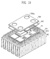
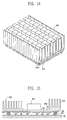
- Fig. 12 is a side view of the multi-chip module 100 to which a lid 58 is attached.
- Figs. 13 and 14 are perspective views of the structure shown in Fig. 12 with the heat sink 42 shown in Fig. 6.
- the lid 58 is attached to the thin-film multi-layer circuit board 32 via a ring-shaped seal member 60 (Fig. 13).
- the lid 58 seals all the LSI chips 14 and other circuit elements 16.
- recesses 58a are formed in the lid 58 to reinforce the lid 58 itself.
- a heat conducting member may be provided between the recesses 58a and the LSI chips 14 in order to radiate heat generated by the LSI chips 14. It is possible to use a lid which seals only some LSI chips 14 and circuit elements 16.
- the lid 58 is made of, for example, a metallic material such as aluminum or covar or a resin.
- the cooling structures which can be applied to the multi-chip module of the present invention are not limited to the aforementioned heat sink 42, but other appropriate cooling structures can be attached to the base board 30.
- a fin-type heat sink of an air cooling type or a water cooling type
- a cold plate of a water cooling type
- a built-in Peltier-effect plate 66 alone or any combinations thereof. If the strength of the base board 30 becomes weak because of attachment of the cooling structure, a conventional supporting member may be used to mount the multi-chip module on the printed wiring board 18.
- the base board supporting the thin-film multi-layer circuit board does not need wiring conductors unlike the base board mounting package used in the prior art, whereby less-expensive multi-chip modules having good operation characteristics can be produced.
- the multi-chip module according to the present invention has a high degree of flexibility in design modifications. That is, the design of the multi-chip module can be modified by changing the thin-film multi-layer structure. Further, a modification of the shape of the multi-chip module can be easily achieved by changing the shape of only the thin-film multi-layer circuit board. Hence, it is possible to greatly reduce the TAT of the design and production of the multi-chip module and the production cost.
Abstract
Description
- The present invention relates to a multi-chip module in which a plurality of circuit elements such as LSI chips are mounted on a high-density wiring board (also referred to as a circuit board).
- Recently, multi-chip modules have become attractive in which a plurality of LSI chips are mounted on a high-density wiring board in order to speed up the operation and reduce the production cost. As is well known, multi-chip modules are classified into three types, namely a MCM-L, MCM-C and MCM-D. The multi-chip modules of the MCM-L type have a printed wiring board on which circuit elements are mounted, and enable reduction in the production cost. The multi-chip modules of the MCM-C type have a thin-film multilayer ceramic board on which circuit elements are mounted, and enable reduction in the production cost and speeding up the operation to some extent. The multi-chip modules of the MCM-D type have a thick-film board made of ceramic or the like, on which a circuit board having at least one multi-layer structure in which an insulating layer and at least one wiring conductor layer are alternately stacked. Circuit elements are mounted on the above circuit board. As compared to the other two types, the MCM-D type multi-chip modules operate at high speeds and enable mounting of circuit elements with a high density.
- Fig. 1 is a side view of a conventional MCM-D type multi-chip module, which includes a thick-film
ceramic board 10 having a multi-layer structure.LSI chips 14 andpassive elements 16 such as resistors and capacitors are mounted on a first surface of the thick-filmceramic board 10. Thesecircuit elements ceramic board 10. A large number of I/O pins 12 are attached to a second surface of theceramic board 10 opposite to the first surface thereof. The multi-chip module is directly mounted on a printedwiring board 18 by inserting the I/O pins 12 into holes formed in the printedwiring board 18. - Fig. 2 is a side view of a conventional MCM-D type multi-chip module. In Fig. 2, parts that are the same as those shown in Fig. 1 are given the same reference numbers as previously. In order to speed up the operation and increase the density, a thin-
film circuit board 20 is provided on the first surface of the thick-filmceramic board 10. Thecircuit elements film circuit board 20, and are connected to the thick-filmceramic board 10 and the I/O pins 12 via wiring lines of the thin-film circuit board 20. On the opposite surfaces of theboards boards wiring board 18 by means of the I/O pins 12 in the same manner as the multi-chip module shown in Fig. 1. - Fig. 3 is a side view of a conventional MCM-D type multi-chip module. In Fig. 3, parts that are the same as those shown in Fig. 2 are given the same reference numbers as previously. The thin-
film circuit board 20 is mounted on abase board 24 which does not have a wiring conductor layer. Thebase board 24 is made of ceramic, a silicon wafer or a metallic material such as aluminum. Thebase board 24 is provided in a baseboard mounting package 22. Thepackage 22 is made of ceramic or mold resin, and a recess portion in which thebase board 24 is accommodated. I/O pins 28 are attached to peripheral portions of thepackage 22 along the edges thereof. The thin-film circuit board 20 and the I/O pins 28 are connected bywires 26. Pads (not shown) for bonding thewires 26 are provided on thepackage 22. The multi-chip module shown in Fig. 3 is mounted on the printedwiring board 18 by means of the I/O pins 28. In the structure shown in Fig. 3, thecircuit elements wiring board 18. - However, the above-mentioned conventional multi-chip modules shown in Figs. 1 through 3 have the following disadvantages.
- The thick-film
ceramic board 10 used in the multi-chip module shown in Fig. 1 has a wiring conductor formation density lower than that of the thin-film circuit board 20 shown in Fig. 2. Hence, a large number of stacked layers is needed to form wiring lines which realize a desired circuit configuration. Further, the larger the number of stacked layers, the longer the wiring lines. This delays transmission of signals. Hence, the structure shown in Fig. 1 is not suitable for circuit configurations particularly needed to operate at high speeds. - The multi-chip module shown in Fig. 2 utilizes the thick-film
ceramic board 10 and the thin-film circuit board 20, and hence has a high production cost. The process of forming the thin-film circuit board 20 greatly depends on the surface condition (warp, roughness, pore and so on) of the ceramic part of the thick-filmceramic board 10 as well as the wiring lines (pad parts) exposed from the ceramic part. Hence, a defect will occur in the thin-film circuit board 20 and a high yield cannot be obtained if the thick-filmceramic board 10 does not have a good surface condition. - The multi-chip module shown in Fig. 3 is advantageous due to use of the
base board 24 made of bulk ceramic, silicon wafer or a metallic material such as aluminum because thebase board 24 can be less expensive and has a good surface condition. However, the multi-chip module shown in Fig. 3 needs thepackage 22 necessary to mount the multi-chip module on the printed wiring board. The use of thepackage 22 increases the production cost. Further, if thepackage 22 does not have good electrical characteristics, signals output from the multi-chip module will be delayed or contain a noise component. These phenomena degrade the performance of the multi-chip module. If there is a demand for an increased number of I/O pins 28 and/or an increased number of circuit elements mounted to thebase board 24 due to a modification of the circuit configuration or the like, thepackage 22 needs to be redesigned. This leads to an increase in the production cost and the time necessary for redesign and reproduction. - Further, the structures shown in Figs. 1 through 3 have a common disadvantage in that the thick-film
ceramic board 10 and the baseboard mounting package 22 need to be redesigned each time the shape of the multi-chip module is modified. This increases the turnaround time of the multi-chip module design and production as well as the production cost. - It is a general object of the present invention to provide a multi-chip module in which the above disadvantages are eliminated.
- A more specific object of the present invention is to provide a less-expensive, high-density, high-speed multi-chip module having high flexibility in the design and production.
- The above objects of the present invention are achieved by a multi-chip module comprising: a base board; a thin-film multi-layer circuit board which is provided on a first surface of the base board and has a multi-layer structure in which insulating layers and wiring conductors are stacked; circuit elements mounted on a main surface of the thin-film multi-layer circuit board; and terminals which are attached to the main surface of the thin-film multi-layer circuit board and electrically connect the wiring conductors to circuits formed on a wiring board on which the multi-chip module is mounted.
- According to the present invention, since the terminals for external connections are attached to the thin-film multi-layer circuit board, the base board supporting the thin-film multi-layer circuit board does not need wiring conductors unlike the base board mounting package used in the prior art, whereby less-expensive multi-chip modules having good operation characteristics can be produced. Further, the multi-chip module according to the present invention has a high degree of flexibility in design modifications. That is, the design of the multi-chip module can be modified by changing the thin-film multi-layer structure. Further, a modification of the shape of the multi-chip module can be easily achieved by changing the shape of only the thin-film multi-layer circuit board. Hence, it is possible to greatly reduce the TAT of the design and production of the multi-chip module and the production cost.
- Other objects, features and advantages of the present invention will become more apparent from the following detailed description when read in conjunction with the accompanying drawings, in which:
- Fig. 1 is a side view of a first conventional multi-chip module;
- Fig. 2 is a side view of a second conventional multi-chip module;
- Fig. 3 is a side view of a third conventional multi-chip module;
- Fig. 4 is a side view of a multi-chip module according to a first embodiment of the present invention;
- Fig. 5 is a cross-sectional view of an essential part of the multi-chip module shown in Fig. 4;
- Fig. 6 is a perspective view of the multi-chip module shown in Fig. 4 viewed from the bottom thereof;
- Fig. 7 is a perspective view of multi-chip modules according to the first embodiment of the present invention on a printed wiring board;
- Fig. 8 is a side view of a multi-chip module according to a second embodiment of the present invention;
- Fig. 9 is a side view of a multi-chip module according to a third embodiment of the present invention;
- Fig. 10 is a side view of a multi-chip module according to a fourth embodiment of the present invention;
- Fig. 11 is a side view of the multi-chip module shown in Fig. 4 with a cover made of resin;
- Fig. 12 is a side view of the multi-chip module shown in Fig. 4 with a cover formed with a lid;
- Fig. 13 is an exploded perspective view of the multi-chip module shown in Fig. 12 with a cooling structure;
- Fig. 14 is a perspective view of the multi-chip module shown in Fig. 12 with a cooling structure attached thereto; and
- Fig. 15 is a side view showing cooling structures that can be applied to the present invention multi-chip module.
-
- A description will now be given, with reference to Figs. 4 and 5, of a
multi-chip module 100 according to a first embodiment of the present invention. Fig. 4 is a side view of themulti-chip module 100, and Fig. 5 is a cross-sectional view of an essential part of themulti-chip module 100 shown in Fig. 4. Themulti-chip module 100 shown in Figs. 4 and 5 is of a PGA (Pin Grid Array) type, and includes abase board 30 and a thin-filmmulti-layer circuit board 32, which is provided on a surface of thebase board 30 facing the printedwiring board 18. - As shown in Fig. 5, the thin-film
multi-layer circuit board 32 has a multi-layer structure, which is made up of afirst wiring conductor 32A-1, asecond wiring conductor 32A-2, athird wiring conductor 32A-3, afourth wiring conductor 32A-4, afifth wiring conductor 32A-5, a first insulatinglayer 32B-1, a second insulatinglayer 32B-2, a thirdinsulating layer 32B-3, a fourth insulatinglayer 32B-4 and a fifth insulatinglayer 32B-5. These conductors and insulating layers are serially stacked on thebase board 30 in the order shown in Fig. 5. Thefirst wiring conductor 32A-1 is provided on thebase board 30. - The
fifth wiring conductor 32A-5 functions as pads used to attach I/O pins 34 andLSI chips 14 thereto. Thepads 32A-5 to which the I/O pins 34 are attached are arranged in an array. Thewiring conductors 32A-1 through 32A-4 extend in the longitudinal and lateral directions (X and Y directions) in the thin-film multi-layer board 32. The wiring conductors located at the different layer levels are electrically connected together by means of a conductor formed in a via hole formed in the insulating layer sandwiched between those wiring conductors. For example, thewiring conductor 32A-1 is connected to thewiring conductor 32A-2 via a viahole 36 formed in the insulatinglayer 32B-1. Thewiring conductor 32A-1 is, for example, a power supply layer. - The thin-film
multi-layer circuit board 32 having the above-mentioned multi-layer structure can be produced by a conventional LSI production process. - The attachment surface of the
pads 32A-5 is exposed from the insulatinglayer 32B-5. The I/O pins 34 are attached to thepads 32A-5 bysolder 38. The areas of thepads 32A-5 exposed from the insulatinglayer 32B-5 are greater than those ofattachment parts 34a of the I/O pins 34. In the structure shown in Fig. 5, thewiring conductor 32A-1 serving as the power supply layer is connected, via a via hole, to the I/O pin 34 located on the left side of the drawing. The first embodiment of the present invention has an essential feature such that the I/O pins 34 inserted into the printedwiring board 18 are attached to the thin-filmmulti-layer wiring board 32. Soldering of the I/O pins 34 can be performed in a conventional manner. - The
LSI chip 14 shown in Fig. 15 is attached to thepad 32A-5 by means of asolder bump 40. Instead of thesolder bump 40, a wire bonding or a TAB (Tape Automated Bonding) lead can be used. - A description will now be given of the materials of the parts of the multi-chip module shown in Figs. 4 and 5. The
base board 30 is made of a ceramic such as AlN, Al₂O₃ or Mulite, a metallic material such as Al, Cu, a Cu-W alloy or the like, Si or glass. Thebase board 30 may be formed of resin used as an insulating material for conventional printed wiring boards, such as glass epoxy or glass polyimide. - The insulating layers 32B-1 through 32B-5 of the thin-film
multi-layer circuit board 32 are made of an organic material such as polyimide, Teflon (trademark), or epoxy. Thewiring conductors 32A-1 through 32A-5 are made of Al, Cu or the like. - The thin-film
multi-layer circuit board 32 is not limited to the structure shown in Fig. 5, but can be a stacked structure in which arbitrary numbers of wiring conductors and insulating layers are alternately stacked. - Fig. 6 is a perspective view of the
multi-chip module 100. The I/O pins 34 are arranged in the peripheral areas of the thin-filmmulti-layer circuit board 32 so as to surround the LSI chips 14 and thepassive elements 16 such as resistors and capacitors. For the sake of simplicity, the illustration of the I/O pins 34 is simplified. On the surface of thebase board 30 opposite to the surface having the thin-filmmulti-layer circuit board 30 is provided a fin-type heat sink 42 for cooling themulti-chip module 100. Theheat sink 42 may have a pipe (not shown) in which coolant water flows. - Fig. 7 is a perspective view of
multi-chip modules 100 which are mounted on the printedwiring board 18. Themulti-chip modules 100 are mounted on a mounting surface of the printedwiring board 18 together withsemiconductor elements 46. A coolingair stream 44 is present, as indicated by the arrows shown in Fig. 7. - Fig. 8 is a side view of a multi-chip module 100A according to a second embodiment of the present invention. In Fig. 8, parts that are the same as those shown in the previously described figures are given the same reference numbers as previously. The multi-chip module 100A shown in Fig. 8 is of a FLT (flat) package type. I/O pins 50 are formed with gull-wing type leads, and are soldered to the
pads 32A-5 shown in Fig. 5. The multi-chip module 100A shown in Fig. 8 has the same advantages as the first embodiment of the present invention. However, the number of attachable I/O pins 50 is less than that of I/O pins 34 of the PGA type. A cooling structure can be applied to the multi-chip module 100A in the same manner as that used in the first embodiment of the present invention. The I/O pins 50 may be TAB leads. - Fig. 9 is a side view of a multi-chip module 100B according to a third embodiment of the present invention. In Fig. 9, parts that are the same as those shown in the previously described figures are given the same reference numbers as previously. The multi-chip module shown in Fig. 9 is of a leadless type such as a BGA (Ball Grid Array) or a LGA (Land Grid Array). Solder bumps 52 are attached to the
pads 32A-5 shown in Fig. 5. For the sake of simplicity, twobumps 52 are respectively shown on the left and right side of the figure. However, bumps 52 can be arranged in an array as in the case of the PGA type. The multi-chip module 100B shown in Fig. 9 has the same advantages as the first embodiment of the present invention. In the LGA type, flat pads are used instead of thebumps 52. A cooling structure can be employed in the same manner as that used in the first embodiment of the present invention. - Fig. 10 is a side view of a multi-chip module 100C according to a fourth embodiment of the present invention. In Fig. 10, parts that are the same as those shown in the previously described figures are given the same reference numbers as previously. The multi-chip module 100C shown in Fig. 10 is of a wire bonding type.
Wires 54 are bonded to thepads 32A-5 shown in Fig. 5. The multi-chip module 100C is directly placed on and in contact with the printedwiring board 18. This mounting is different from the mounting according to the first through third embodiments of the present invention. The fourth embodiment of the present invention cannot employ a cooling structure similar to that used in the first through third embodiments of the present invention. The multi-chip module 100C is cooled via the printedwiring board 18. - The I/O terminals of the present invention are not limited to the above-mentioned types, and other types of I/O terminals can be used.
- Fig. 11 is a side view of the
multi-chip module 100 to which acover 56 made of resin is attached. Thecover 56 is provided so that it seals the LSI chips 14 and thecircuit elements 16. Theresin cover 56 is made of, for example, epoxy-based resin or a silicon-based resin (potting). Theresin cover 56 can be provided so that it seals only some of the LSI chips 14 and thecircuit elements 16. Thecover 56 can be applied to the second through fourth embodiments of the present invention in the same manner as described above. - Fig. 12 is a side view of the
multi-chip module 100 to which alid 58 is attached. Figs. 13 and 14 are perspective views of the structure shown in Fig. 12 with theheat sink 42 shown in Fig. 6. Thelid 58 is attached to the thin-filmmulti-layer circuit board 32 via a ring-shaped seal member 60 (Fig. 13). In the structure shown in Figs. 12 and 13, thelid 58 seals all the LSI chips 14 andother circuit elements 16. As shown in Fig. 13, recesses 58a are formed in thelid 58 to reinforce thelid 58 itself. A heat conducting member may be provided between therecesses 58a and the LSI chips 14 in order to radiate heat generated by the LSI chips 14. It is possible to use a lid which seals only someLSI chips 14 andcircuit elements 16. Thelid 58 is made of, for example, a metallic material such as aluminum or covar or a resin. - The cooling structures which can be applied to the multi-chip module of the present invention are not limited to the
aforementioned heat sink 42, but other appropriate cooling structures can be attached to thebase board 30. For example, as shown in Fig. 15, it is possible to use a fin-type heat sink (of an air cooling type or a water cooling type) 62, a cold plate (of a water cooling type) 64 or a built-in Peltier-effect plate 66 alone or any combinations thereof. If the strength of thebase board 30 becomes weak because of attachment of the cooling structure, a conventional supporting member may be used to mount the multi-chip module on the printedwiring board 18. - According to the present invention, since the I/O terminals for external connections are attached to the thin-film multi-layer circuit board, the base board supporting the thin-film multi-layer circuit board does not need wiring conductors unlike the base board mounting package used in the prior art, whereby less-expensive multi-chip modules having good operation characteristics can be produced. Further, the multi-chip module according to the present invention has a high degree of flexibility in design modifications. That is, the design of the multi-chip module can be modified by changing the thin-film multi-layer structure. Further, a modification of the shape of the multi-chip module can be easily achieved by changing the shape of only the thin-film multi-layer circuit board. Hence, it is possible to greatly reduce the TAT of the design and production of the multi-chip module and the production cost.
- The present invention is not limited to the specifically disclosed embodiments, and variations and modifications may be made without departing from the scope of the present invention.
Claims (12)
- A multi-chip module comprising:
a base board (30);
a thin-film multi-layer circuit board (32) which is provided on a first surface of the base board and has a multi-layer structure in which insulating layers and wiring conductors are stacked;
circuit elements (32A-5) mounted on a main surface of the thin-film multi-layer circuit board; and
terminals (34) which are attached to the main surface of the thin-film multi-layer circuit board and electrically connect the wiring conductors to circuits formed on a wiring board on which the multi-chip module is mounted. - The multi-chip module as claimed in claim 1, characterized in that said terminals comprise lead members.
- The multi-chip module as claimed in claim 1, characterized in that said terminals comprise leadless members.
- The multi-chip module as claimed in claim 1, 2 or 3, characterized in that said terminals are soldered to wiring conductors of the thin-film multilayer circuit board facing the wiring board, so that the terminals are supported by the thin-film multilayer circuit board.
- The multi-chip module as claimed in any of claims 1 to 4, characterized in that wiring conductors of the thin-film multi-layer circuit board facing the wiring board comprise pad areas to which said terminals are connected.
- The multi-chip module as claimed in claim 2, characterized in that said lead members comprise lead pins vertically extending from the main surface of the thin-film multi-layer circuit board.
- The multi-chip module as claimed in claim 2, characterized in that said lead members comprise flat-type lead pins.
- The multi-chip module as claimed in claim 2, characterized in that said lead members comprise wire leads.
- The multi-chip module as claimed in claim 2, characterized in that said lead members comprise tape-automated bonding leads.
- The multi-chip module as claimed in any of claims 1 to 5, characterized in that said terminals are located in peripheral areas on the main surface of the thin-film multi-layer circuit board so that said terminals surround the circuit elements.
- The multi-chip module as claimed in any of claims 1 to 5 or claim 10, characterized by further comprising a cover which is formed on the main surface of the thin-film multi-layer circuit board and covers the circuit elements.
- The multi-chip module as claimed in any of claims 1 to 5 or claims 10 or 11, characterized by further comprising a cooling structure which is formed on a second surface of the base board opposite to the first surface thereof and which cools the multi-chip module.
Applications Claiming Priority (3)
| Application Number | Priority Date | Filing Date | Title |
|---|---|---|---|
| JP05200736A JP3110922B2 (en) | 1993-08-12 | 1993-08-12 | Multi-chip module |
| JP200736/93 | 1993-08-12 | ||
| JP20073693 | 1993-08-12 |
Publications (3)
| Publication Number | Publication Date |
|---|---|
| EP0638931A2 true EP0638931A2 (en) | 1995-02-15 |
| EP0638931A3 EP0638931A3 (en) | 1995-05-10 |
| EP0638931B1 EP0638931B1 (en) | 2004-04-28 |
Family
ID=16429325
Family Applications (1)
| Application Number | Title | Priority Date | Filing Date |
|---|---|---|---|
| EP19940400928 Expired - Lifetime EP0638931B1 (en) | 1993-08-12 | 1994-04-29 | Multi-chip module |
Country Status (4)
| Country | Link |
|---|---|
| US (1) | US5586006A (en) |
| EP (1) | EP0638931B1 (en) |
| JP (1) | JP3110922B2 (en) |
| DE (1) | DE69433736T2 (en) |
Cited By (7)
| Publication number | Priority date | Publication date | Assignee | Title |
|---|---|---|---|---|
| GB2307596A (en) * | 1995-11-21 | 1997-05-28 | Murata Manufacturing Co | Radio communications module |
| US5872700A (en) * | 1996-07-11 | 1999-02-16 | Nokia Mobile Phones Limited | Multi-chip module package with insulating tape having electrical leads and solder bumps |
| EP0986099A2 (en) * | 1998-09-08 | 2000-03-15 | Lucent Technologies Inc. | Translator for recessed flip-chip package |
| WO2003030255A2 (en) * | 2001-10-03 | 2003-04-10 | Formfactor, Inc. | Multiple die interconnect system |
| AT411509B (en) * | 1999-09-17 | 2004-01-26 | Telekom Austria Ag | ARRANGEMENT AND METHOD FOR ENCLOSED COMMUNICATION |
| EP1720385A2 (en) * | 1998-12-16 | 2006-11-08 | Ibiden Co., Ltd. | Conductive connecting pin and package substrate |
| CN102905465A (en) * | 2011-07-26 | 2013-01-30 | 鸿富锦精密工业(深圳)有限公司 | Double-sided circuit board structure |
Families Citing this family (29)
| Publication number | Priority date | Publication date | Assignee | Title |
|---|---|---|---|---|
| US5675310A (en) * | 1994-12-05 | 1997-10-07 | General Electric Company | Thin film resistors on organic surfaces |
| WO1997030461A1 (en) * | 1996-02-15 | 1997-08-21 | Bourns, Inc. | Resistor network in ball grid array package |
| US5842877A (en) * | 1996-12-16 | 1998-12-01 | Telefonaktiebolaget L M Ericsson | Shielded and impedance-matched connector assembly, and associated method, for radio frequency circuit device |
| JP3340350B2 (en) * | 1997-04-18 | 2002-11-05 | 富士通株式会社 | Thin film multilayer substrate and electronic device |
| JP4480207B2 (en) * | 1999-01-04 | 2010-06-16 | イビデン株式会社 | Resin package substrate |
| JP4554741B2 (en) * | 1999-01-04 | 2010-09-29 | イビデン株式会社 | Package substrate |
| JP2010226122A (en) * | 1999-01-04 | 2010-10-07 | Ibiden Co Ltd | Package board |
| JP2000323599A (en) * | 1999-05-13 | 2000-11-24 | Nec Corp | Package structure for lsi |
| US6196002B1 (en) | 1999-06-24 | 2001-03-06 | Advanced Micro Devices, Inc. | Ball grid array package having thermoelectric cooler |
| KR20080031522A (en) | 2000-02-25 | 2008-04-08 | 이비덴 가부시키가이샤 | Multilayer printed wiring board and method for producing multilayer printed wiring board |
| US6465085B1 (en) * | 2000-04-04 | 2002-10-15 | Fujitsu Limited | Thin film wiring board and method for manufacturing the same, base substrate and method for manufacturing the same |
| CN100539106C (en) | 2000-09-25 | 2009-09-09 | 揖斐电株式会社 | Semiconductor element and manufacture method thereof, multilayer printed-wiring board and manufacture method thereof |
| US6576489B2 (en) * | 2001-05-07 | 2003-06-10 | Applied Materials, Inc. | Methods of forming microstructure devices |
| US6528892B2 (en) * | 2001-06-05 | 2003-03-04 | International Business Machines Corporation | Land grid array stiffener use with flexible chip carriers |
| US7042084B2 (en) * | 2002-01-02 | 2006-05-09 | Intel Corporation | Semiconductor package with integrated heat spreader attached to a thermally conductive substrate core |
| US6897761B2 (en) * | 2002-12-04 | 2005-05-24 | Cts Corporation | Ball grid array resistor network |
| TW577153B (en) * | 2002-12-31 | 2004-02-21 | Advanced Semiconductor Eng | Cavity-down MCM package |
| JP2004228478A (en) * | 2003-01-27 | 2004-08-12 | Fujitsu Ltd | Printed wiring board |
| US6807061B1 (en) * | 2003-04-28 | 2004-10-19 | Hewlett-Packard Development Company, L.P. | Stack up assembly |
| JP4559777B2 (en) * | 2003-06-26 | 2010-10-13 | 株式会社東芝 | Semiconductor device and manufacturing method thereof |
| US20050128710A1 (en) * | 2003-12-15 | 2005-06-16 | Beiteimal Abdlmonem H. | Cooling system for electronic components |
| US7342804B2 (en) * | 2004-08-09 | 2008-03-11 | Cts Corporation | Ball grid array resistor capacitor network |
| DE102005013762C5 (en) | 2005-03-22 | 2012-12-20 | Sew-Eurodrive Gmbh & Co. Kg | Electronic device and method for determining the temperature of a power semiconductor |
| CN101287986B (en) | 2005-06-14 | 2012-01-18 | 三美电机株式会社 | Field effect transistor, biosensor provided with it, and detecting method |
| JP4498991B2 (en) * | 2005-07-15 | 2010-07-07 | 新光電気工業株式会社 | Semiconductor device and electronic device |
| US20070164428A1 (en) * | 2006-01-18 | 2007-07-19 | Alan Elbanhawy | High power module with open frame package |
| TWI399845B (en) * | 2009-09-24 | 2013-06-21 | Powertech Technology Inc | Multi-chip stacked device without loop height and its manufacturing method |
| US10211122B2 (en) * | 2014-12-26 | 2019-02-19 | Mitsubishi Electric Corporation | Semiconductor module including a case and base board |
| JP7015691B2 (en) * | 2017-12-27 | 2022-02-03 | 新光電気工業株式会社 | Semiconductor device |
Citations (6)
| Publication number | Priority date | Publication date | Assignee | Title |
|---|---|---|---|---|
| EP0098932A2 (en) * | 1982-07-08 | 1984-01-25 | International Business Machines Corporation | Repairable multi-level system for semiconductor device |
| FR2557755A1 (en) * | 1983-12-28 | 1985-07-05 | Nec Corp | MULTI-LAYER WIRING SUBSTRATE |
| EP0475223A2 (en) * | 1990-08-31 | 1992-03-18 | Nec Corporation | Method of fabricating integrated circuit chip package |
| US5130768A (en) * | 1990-12-07 | 1992-07-14 | Digital Equipment Corporation | Compact, high-density packaging apparatus for high performance semiconductor devices |
| EP0509825A2 (en) * | 1991-04-16 | 1992-10-21 | Nec Corporation | Package structure for semiconductor device |
| EP0540247A2 (en) * | 1991-10-28 | 1993-05-05 | International Business Machines Corporation | Formulation of multichip modules |
Family Cites Families (9)
| Publication number | Priority date | Publication date | Assignee | Title |
|---|---|---|---|---|
| US4389862A (en) * | 1980-09-23 | 1983-06-28 | Hastings Thomas M | High security locking assembly for lockrods type rear-end closures of cargo vehicles |
| FR2621173B1 (en) * | 1987-09-29 | 1989-12-08 | Bull Sa | HIGH DENSITY INTEGRATED CIRCUIT BOX |
| US5258649A (en) * | 1989-05-20 | 1993-11-02 | Hitachi, Ltd. | Semiconductor device and electronic apparatus using semiconductor device |
| JP2978511B2 (en) * | 1989-09-20 | 1999-11-15 | 株式会社日立製作所 | Integrated circuit element mounting structure |
| US5155661A (en) * | 1991-05-15 | 1992-10-13 | Hewlett-Packard Company | Aluminum nitride multi-chip module |
| US5256469A (en) * | 1991-12-18 | 1993-10-26 | General Electric Company | Multi-layered, co-fired, ceramic-on-metal circuit board for microelectronic packaging |
| US5306670A (en) * | 1993-02-09 | 1994-04-26 | Texas Instruments Incorporated | Multi-chip integrated circuit module and method for fabrication thereof |
| JP2531464B2 (en) * | 1993-12-10 | 1996-09-04 | 日本電気株式会社 | Semiconductor package |
| US5432679A (en) * | 1994-05-31 | 1995-07-11 | The Whitaker Corporation | Pressure equalizer for an integrated circuit chip interconnected to circuitry on a thin film membrane |
-
1993
- 1993-08-12 JP JP05200736A patent/JP3110922B2/en not_active Expired - Fee Related
-
1994
- 1994-04-29 EP EP19940400928 patent/EP0638931B1/en not_active Expired - Lifetime
- 1994-04-29 DE DE1994633736 patent/DE69433736T2/en not_active Expired - Lifetime
-
1995
- 1995-12-15 US US08/573,577 patent/US5586006A/en not_active Expired - Lifetime
Patent Citations (6)
| Publication number | Priority date | Publication date | Assignee | Title |
|---|---|---|---|---|
| EP0098932A2 (en) * | 1982-07-08 | 1984-01-25 | International Business Machines Corporation | Repairable multi-level system for semiconductor device |
| FR2557755A1 (en) * | 1983-12-28 | 1985-07-05 | Nec Corp | MULTI-LAYER WIRING SUBSTRATE |
| EP0475223A2 (en) * | 1990-08-31 | 1992-03-18 | Nec Corporation | Method of fabricating integrated circuit chip package |
| US5130768A (en) * | 1990-12-07 | 1992-07-14 | Digital Equipment Corporation | Compact, high-density packaging apparatus for high performance semiconductor devices |
| EP0509825A2 (en) * | 1991-04-16 | 1992-10-21 | Nec Corporation | Package structure for semiconductor device |
| EP0540247A2 (en) * | 1991-10-28 | 1993-05-05 | International Business Machines Corporation | Formulation of multichip modules |
Non-Patent Citations (3)
| Title |
|---|
| 1992 IEEE Multi-Chip Module Conference, MCMC-92, * |
| IEEE TRANSACTIONS ON COMPONENTS,HYBRIDS,AND MANUFACTURING TECHNOLOGY, vol.12, no.4, December 1989, NEW YORK US pages 658 - 662 S. SASAKI ET AL. 'A New Multichip Module Using a Copper Polyimide Multilayer Substrate' * |
| RESEARCH DISCLOSURE, no.326, June 1991, HAVANT GB page 401 'Low Profile Chip Package' * |
Cited By (19)
| Publication number | Priority date | Publication date | Assignee | Title |
|---|---|---|---|---|
| GB2307596A (en) * | 1995-11-21 | 1997-05-28 | Murata Manufacturing Co | Radio communications module |
| US5872700A (en) * | 1996-07-11 | 1999-02-16 | Nokia Mobile Phones Limited | Multi-chip module package with insulating tape having electrical leads and solder bumps |
| EP0986099A3 (en) * | 1998-09-08 | 2005-06-29 | Lucent Technologies Inc. | Translator for recessed flip-chip package |
| EP0986099A2 (en) * | 1998-09-08 | 2000-03-15 | Lucent Technologies Inc. | Translator for recessed flip-chip package |
| EP1924130A3 (en) * | 1998-12-16 | 2010-11-17 | Ibiden Co., Ltd. | Conductive connecting pin and package substrate |
| US7902659B2 (en) | 1998-12-16 | 2011-03-08 | Ibiden Co., Ltd. | Conductive connecting pin and package substrate |
| US8536696B2 (en) | 1998-12-16 | 2013-09-17 | Ibiden Co., Ltd. | Conductive pin attached to package substrate |
| US8110917B2 (en) | 1998-12-16 | 2012-02-07 | Ibiden Co., Ltd. | Package substrate with a conductive connecting pin |
| EP1720385A2 (en) * | 1998-12-16 | 2006-11-08 | Ibiden Co., Ltd. | Conductive connecting pin and package substrate |
| EP1845759A1 (en) * | 1998-12-16 | 2007-10-17 | Ibiden Co., Ltd. | Conductive connecting pin and package substrate |
| EP1924130A2 (en) * | 1998-12-16 | 2008-05-21 | Ibiden Co., Ltd. | Conductive connecting pin and package substrate |
| US8035214B1 (en) | 1998-12-16 | 2011-10-11 | Ibiden Co., Ltd. | Conductive connecting pin for package substance |
| US7847393B2 (en) | 1998-12-16 | 2010-12-07 | Ibiden Co., Ltd. | Conductive connecting pins for a package substrate |
| AT411509B (en) * | 1999-09-17 | 2004-01-26 | Telekom Austria Ag | ARRANGEMENT AND METHOD FOR ENCLOSED COMMUNICATION |
| WO2003030255A2 (en) * | 2001-10-03 | 2003-04-10 | Formfactor, Inc. | Multiple die interconnect system |
| US7681309B2 (en) | 2001-10-03 | 2010-03-23 | Formfactor, Inc. | Method for interconnecting an integrated circuit multiple die assembly |
| WO2003030255A3 (en) * | 2001-10-03 | 2003-10-30 | Formfactor Inc | Multiple die interconnect system |
| US6882546B2 (en) | 2001-10-03 | 2005-04-19 | Formfactor, Inc. | Multiple die interconnect system |
| CN102905465A (en) * | 2011-07-26 | 2013-01-30 | 鸿富锦精密工业(深圳)有限公司 | Double-sided circuit board structure |
Also Published As
| Publication number | Publication date |
|---|---|
| DE69433736T2 (en) | 2004-09-30 |
| JPH0758276A (en) | 1995-03-03 |
| EP0638931A3 (en) | 1995-05-10 |
| US5586006A (en) | 1996-12-17 |
| EP0638931B1 (en) | 2004-04-28 |
| JP3110922B2 (en) | 2000-11-20 |
| DE69433736D1 (en) | 2004-06-03 |
Similar Documents
| Publication | Publication Date | Title |
|---|---|---|
| US5586006A (en) | Multi-chip module having a multi-layer circuit board with insulating layers and wiring conductors stacked together | |
| US5525834A (en) | Integrated circuit package | |
| US5701032A (en) | Integrated circuit package | |
| US5247423A (en) | Stacking three dimensional leadless multi-chip module and method for making the same | |
| EP0617465B1 (en) | A semiconductor device and package | |
| US5620928A (en) | Ultra thin ball grid array using a flex tape or printed wiring board substrate and method | |
| JP3239909B2 (en) | Stackable 3D multi-chip semiconductor device and its manufacturing method | |
| US5468994A (en) | High pin count package for semiconductor device | |
| US6218731B1 (en) | Tiny ball grid array package | |
| US6525942B2 (en) | Heat dissipation ball grid array package | |
| US5763947A (en) | Integrated circuit chip package having configurable contacts and a removable connector | |
| US6449159B1 (en) | Semiconductor module with imbedded heat spreader | |
| US5777345A (en) | Multi-chip integrated circuit package | |
| USRE42332E1 (en) | Integrated circuit package, ball-grid array integrated circuit package | |
| US5684330A (en) | Chip-sized package having metal circuit substrate | |
| JP2910670B2 (en) | Semiconductor mounting structure | |
| US7161251B2 (en) | Partially populated ball grid design to accommodate landing pads close to the die | |
| US5796038A (en) | Technique to produce cavity-up HBGA packages | |
| US5742477A (en) | Multi-chip module | |
| US4964019A (en) | Multilayer bonding and cooling of integrated circuit devices | |
| US6057594A (en) | High power dissipating tape ball grid array package | |
| KR100196991B1 (en) | Chip scale package assembly and multi chip module assembly | |
| US6137174A (en) | Hybrid ASIC/memory module package | |
| US6963129B1 (en) | Multi-chip package having a contiguous heat spreader assembly | |
| KR100276858B1 (en) | Electronic package with enhanced pad design |
Legal Events
| Date | Code | Title | Description |
|---|---|---|---|
| PUAI | Public reference made under article 153(3) epc to a published international application that has entered the european phase |
Free format text: ORIGINAL CODE: 0009012 |
|
| AK | Designated contracting states |
Kind code of ref document: A2 Designated state(s): DE FR GB |
|
| PUAL | Search report despatched |
Free format text: ORIGINAL CODE: 0009013 |
|
| AK | Designated contracting states |
Kind code of ref document: A3 Designated state(s): DE FR GB |
|
| 17P | Request for examination filed |
Effective date: 19950601 |
|
| 17Q | First examination report despatched |
Effective date: 19960628 |
|
| APAB | Appeal dossier modified |
Free format text: ORIGINAL CODE: EPIDOS NOAPE |
|
| APAB | Appeal dossier modified |
Free format text: ORIGINAL CODE: EPIDOS NOAPE |
|
| APAD | Appeal reference recorded |
Free format text: ORIGINAL CODE: EPIDOS REFNE |
|
| GRAP | Despatch of communication of intention to grant a patent |
Free format text: ORIGINAL CODE: EPIDOSNIGR1 |
|
| GRAS | Grant fee paid |
Free format text: ORIGINAL CODE: EPIDOSNIGR3 |
|
| GRAA | (expected) grant |
Free format text: ORIGINAL CODE: 0009210 |
|
| AK | Designated contracting states |
Kind code of ref document: B1 Designated state(s): DE FR GB |
|
| REG | Reference to a national code |
Ref country code: GB Ref legal event code: FG4D |
|
| REF | Corresponds to: |
Ref document number: 69433736 Country of ref document: DE Date of ref document: 20040603 Kind code of ref document: P |
|
| ET | Fr: translation filed | ||
| PLBE | No opposition filed within time limit |
Free format text: ORIGINAL CODE: 0009261 |
|
| STAA | Information on the status of an ep patent application or granted ep patent |
Free format text: STATUS: NO OPPOSITION FILED WITHIN TIME LIMIT |
|
| 26N | No opposition filed |
Effective date: 20050131 |
|
| APAH | Appeal reference modified |
Free format text: ORIGINAL CODE: EPIDOSCREFNO |
|
| PGFP | Annual fee paid to national office [announced via postgrant information from national office to epo] |
Ref country code: FR Payment date: 20110426 Year of fee payment: 18 Ref country code: DE Payment date: 20110427 Year of fee payment: 18 |
|
| PGFP | Annual fee paid to national office [announced via postgrant information from national office to epo] |
Ref country code: GB Payment date: 20110427 Year of fee payment: 18 |
|
| GBPC | Gb: european patent ceased through non-payment of renewal fee |
Effective date: 20120429 |
|
| REG | Reference to a national code |
Ref country code: FR Ref legal event code: ST Effective date: 20121228 |
|
| PG25 | Lapsed in a contracting state [announced via postgrant information from national office to epo] |
Ref country code: GB Free format text: LAPSE BECAUSE OF NON-PAYMENT OF DUE FEES Effective date: 20120429 |
|
| REG | Reference to a national code |
Ref country code: DE Ref legal event code: R119 Ref document number: 69433736 Country of ref document: DE Effective date: 20121101 |
|
| PG25 | Lapsed in a contracting state [announced via postgrant information from national office to epo] |
Ref country code: FR Free format text: LAPSE BECAUSE OF NON-PAYMENT OF DUE FEES Effective date: 20120430 |
|
| PG25 | Lapsed in a contracting state [announced via postgrant information from national office to epo] |
Ref country code: DE Free format text: LAPSE BECAUSE OF NON-PAYMENT OF DUE FEES Effective date: 20121101 |