EP0640980A2 - Semiconductor memory having a plurality of banks - Google Patents
Semiconductor memory having a plurality of banks Download PDFInfo
- Publication number
- EP0640980A2 EP0640980A2 EP94111301A EP94111301A EP0640980A2 EP 0640980 A2 EP0640980 A2 EP 0640980A2 EP 94111301 A EP94111301 A EP 94111301A EP 94111301 A EP94111301 A EP 94111301A EP 0640980 A2 EP0640980 A2 EP 0640980A2
- Authority
- EP
- European Patent Office
- Prior art keywords
- bank
- address signal
- banks
- signal
- semiconductor memory
- Prior art date
- Legal status (The legal status is an assumption and is not a legal conclusion. Google has not performed a legal analysis and makes no representation as to the accuracy of the status listed.)
- Granted
Links
Images


Classifications
-
- G—PHYSICS
- G06—COMPUTING; CALCULATING OR COUNTING
- G06F—ELECTRIC DIGITAL DATA PROCESSING
- G06F12/00—Accessing, addressing or allocating within memory systems or architectures
- G06F12/02—Addressing or allocation; Relocation
- G06F12/06—Addressing a physical block of locations, e.g. base addressing, module addressing, memory dedication
- G06F12/0615—Address space extension
- G06F12/0623—Address space extension for memory modules
-
- G—PHYSICS
- G11—INFORMATION STORAGE
- G11C—STATIC STORES
- G11C8/00—Arrangements for selecting an address in a digital store
- G11C8/12—Group selection circuits, e.g. for memory block selection, chip selection, array selection
-
- G—PHYSICS
- G11—INFORMATION STORAGE
- G11C—STATIC STORES
- G11C11/00—Digital stores characterised by the use of particular electric or magnetic storage elements; Storage elements therefor
- G11C11/21—Digital stores characterised by the use of particular electric or magnetic storage elements; Storage elements therefor using electric elements
- G11C11/34—Digital stores characterised by the use of particular electric or magnetic storage elements; Storage elements therefor using electric elements using semiconductor devices
- G11C11/40—Digital stores characterised by the use of particular electric or magnetic storage elements; Storage elements therefor using electric elements using semiconductor devices using transistors
- G11C11/401—Digital stores characterised by the use of particular electric or magnetic storage elements; Storage elements therefor using electric elements using semiconductor devices using transistors forming cells needing refreshing or charge regeneration, i.e. dynamic cells
- G11C11/4063—Auxiliary circuits, e.g. for addressing, decoding, driving, writing, sensing or timing
- G11C11/407—Auxiliary circuits, e.g. for addressing, decoding, driving, writing, sensing or timing for memory cells of the field-effect type
- G11C11/408—Address circuits
- G11C11/4087—Address decoders, e.g. bit - or word line decoders; Multiple line decoders
-
- G—PHYSICS
- G11—INFORMATION STORAGE
- G11C—STATIC STORES
- G11C8/00—Arrangements for selecting an address in a digital store
- G11C8/10—Decoders
-
- G—PHYSICS
- G11—INFORMATION STORAGE
- G11C—STATIC STORES
- G11C8/00—Arrangements for selecting an address in a digital store
- G11C8/18—Address timing or clocking circuits; Address control signal generation or management, e.g. for row address strobe [RAS] or column address strobe [CAS] signals
Definitions
- the present invention relates to a semiconductor memory, and more particularly, to a semiconductor memory having a plurality of memory cell areas called banks.
- SDRAM synchronous dynamic random access memory
- a SDRAM having two banks when one bank carries out an active operation, the other bank simultaneously carries out a precharge operation, so that the total operation speed becomes high.
- a SDRAM having a plurality of banks is used for a cache memory of a computer system, so as to accelerate the cache operation thereof.
- the configuration of the SDRAM i.e., the number of the banks, is determined in accordance with the requirement of the computer system, or the configuration of the computer system using the SDRAM.
- An embodiment of the present invention may provide a semiconductor memory having a plurality of banks and able to serve as a memory having a smaller number of banks.
- a semiconductor memory comprising a plurality of banks, each of the banks having a plurality of memory cells, and a specific memory cell of a specific bank being selected in accordance with a first address signal and a second address signal successively provided to the semiconductor memory; a first specify unit for specifying one of the plurality of banks by decoding a bank address signal contained in the first address signal; and a second specify unit for specifying one of the plurality of banks by decoding the bank address signal contained in the first address signal, according to bank status signals that indicates whether or not each of the banks is activated, so that the semiconductor memory is used for different bank configurations.
- the semiconductor memory may be a dynamic random access memory, or a synchronous dynamic random access memory.
- a bank activation instruction and a read instruction may be provided with a clock enable signal, a chip select signal, a row address strobe signal, a column address strobe signal, and a write enable signal.
- the semiconductor memory may further comprise a plurality of drivers for driving corresponding word decoders and sense amplifiers, and the bank status signals may be output from the drivers.
- the banks may maintain an active state if required even under an unselected state after a read operation or a write operation.
- the first address signal may be a row address signal
- the second address signal may be a column address signal.
- the number of the banks may be determined as 2 x , where x being an integer equal to or greater than two; the bank configurations may include a first bank configuration and a second bank configuration, the first bank configuration being 2 x and the second bank configuration being 2 y , where y being an integer equal to or greater than one and obtained by dividing the x by a multiple of two.
- the first specify unit may decode an x-bit bank address signal contained in the first address signal, to specify one of the 2 x banks functioning as they are or as 2 y banks; and the second specify unit may decode, according to information signals indicating whether or not each of the 2 x banks is active, an x-bit bank address signal contained in the second address signal if the 2 x banks function as they are or a y-bit bank address signal contained in the second address signal if the 2 x banks function as 2 y banks, to specify the bank that has been specified according to the first address signal, so that data are written into or read out of the specified bank.
- a semiconductor memory having 2 x banks, where x being an integer equal to or greater than two, that maintain an active state if required even under an unselected state after a read or write operation, any memory cell in any one of the banks being selectable according to a first address signal and a second address signal successively provided to the semiconductor memory
- the semiconductor memory comprises a first specify unit for decoding an x-bit bank address signal contained in the first address signal, to specify one of the 2 x banks functioning as they are or as 2 y banks, where y being an integer equal to or greater than one and obtained by dividing the x by a multiple of two, so that a word line is selected in the specified bank; and a second specify unit for decoding, according to information signals indicating whether or not each of the 2 x banks is active, an x-bit bank address signal contained in the second address signal if the 2 x banks function as they are or a y-bit bank address signal contained in the second address signal if the 2 x
- FIGS 1A and 1B show parts of a semiconductor memory (SDRAM: synchronous dynamic random access memory )according to the prior art. Note that this semiconductor memory is a four-bank SDRAM employing four banks to operate in synchronism with external clock signals.
- SDRAM synchronous dynamic random access memory
- reference numerals 1 to 4 denote memory cell areas, i.e., banks that maintain an active state if required even under an unselected state after a write or read operation
- 5 to 8 denote word decoders provided for corresponding banks, respectively, to decode an address signal to specify a word line in the banks.
- reference numerals 9 to 12 denotes sense amplifiers
- 13 to 16 denotes column decoders
- 17 denotes a bank address buffer
- 18 denotes a bank decoder
- 19 to 22 denotes drivers.
- reference numeral 23 denotes an address buffer
- 24 denotes a selector
- 25 denotes a selector.
- the column decoders 13 to 16 are used to decode a column address signal for specifying a column in the banks 1 to 4, and the sense amplifiers 9 to 12 are used to amplify data read out from the banks 1 to 4.
- the bank address buffer 17 is used to receive a bank address signal of bits BA0 and BA1 for selecting one of the banks 1 to 4, and the bank decoder 18 is used to decode the bank address signal.
- One of the drivers 19 to 22 is activated to drive the word decoder and sense amplifier of a selected bank, according to the decoded signal provided by the bank decoder 18.
- the address buffer 23 is used to receive an address signal of bits A0 to An, and the selector 24 is used to supply a word line selecting address signal (which is provided by the address buffer 23) to the word decoder of the bank specified by the decoded signal from the bank decoder 18.
- the selector 25 is used to supply a column address signal provided by the address buffer 23 to the column decoder of the bank specified by the decoded signal from the bank decoder 18.
- reference numerals 26 to 29 denotes amplifiers
- 30 to 33 denotes write circuits
- 34 denotes a selector
- reference numeral 35 denotes an output buffer
- 36 denotes an input buffer
- 37 denotes a selector
- 37 denotes a selector
- 38 denotes an operation controller.
- reference mark CLK denotes a clock signal
- /RAS denotes a row address strobe signal
- /CAS denotes a column address strobe signal
- /WE denotes a write enable signal
- /CS denotes a chip select signal
- CKE denotes a clock enable signal.
- the mark "/" indicates a low enable signal or a low active signal, and thus, for example, the chip select signal /CS is at a low level "L", the chip being supplied with the chip select signal /CS of "L" is selected.
- the amplifiers 26 to 29 are used to amplify data read through the sense amplifiers 9 to 12, and the write circuits 30 to 33 are used to write data into the banks 1 to 4.
- the selector 34 is used to select one of the amplifiers 26 to 29 of the bank specified by the decoded signal from the bank decoder 18.
- the output buffer 35 is used to latch data from the selector 34 and provide the same outside, and the input buffer 36 is used to store write data provided from the outside.
- the selector 37 is used to supply the write data from the input buffer 36 to one of the write circuits 30 to 33 of the bank specified by the decoded signal from the bank decoder 18.
- the operation controller 38 is used to control the operation timing of the elements mentioned above according to external control signals, and the clock enable signal CKE is used to enable the clock signal CLK.
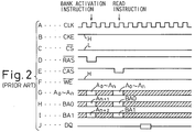
- FIG. 2 is a timechart showing a read operation of the semiconductor memory (SDRAM) shown in Figs. 1A and 1B.
- a reference mark A represents the clock signal CLK
- B the clock enable signal CKE
- C the chip select signal /CS
- D the row address strobe signal /RAS
- E the column address strobe signal /CAS
- F the write enable signal /WE.
- a reference mark G represents an address signal of bits A0 to An
- H the bit BA0 of a bank address signal
- I the bit BA1 of the bank address signal
- J output data DQ.
- the SDRAM latches the externally supplied signals in response to a rise of the clock signal CLK.
- the SDRAM firstly receives a bank activation instruction and row address signal.
- the bank activation instruction is provided with the clock enable signal CKE of a high level "H”, chip select signal /CS of a low level “L”, row address strobe signal /RAS of the low level “L”, column address strobe signal /CAS of the high level "H”, and write enable signal /WE of the high level "H”.
- the row address signal involves bits A0 to An+2.
- the bits An+1 and An+2 are latched as the bits BA0 and BA1 of the bank address signal by the bank address buffer 17, and the bits A0 to An are latched by the address buffer 23.
- the bank address signal of bits BA0 and BA1 latched by the bank address buffer 17 are changed to complementary signals, and the complementary signals are supplied to the bank decoder 18 and decoded therein.
- the decoded signals are supplied to the drivers 19 to 22 and selectors 24, 25, 34, and 37. At this time, the selectors 25, 34, and 37 are controlled to ignore the decoded signal.
- One of the drivers 19 to 22 corresponding to the decoded signal activates the corresponding word decoder and sense amplifier, to make the corresponding bank ready to be read.
- the bits A0 to An of the row address signal latched by the address buffer 23 are transferred to one of the word decoders 5 to 8 corresponding to the selected bank through the selector 24, so that a word line is selected in the bank.
- the SDRAM then receives a read instruction.
- the read instruction is provided with the clock enable signal CKE of "H”, chip selector signal /CS of "L”, row address strobe signal /RAS of "H”, column address strobe signal /CAS of "L”, and write enable signal /WE of "H”.
- a bank address signal of bits BA0 and BA1 is latched by the bank address buffer 17, and a column address signal of bits A0 to An is latched by the address buffer 23.
- the bank address signal of bits BA0 and BA1 latched by the bank address buffer 17 becomes a complementary signal, which is decoded by the bank decoder 18.
- the decoded signal is supplied to the drivers 19 to 22 and selectors 24, 25, 34, and 37. At this time, the drivers 19 to 22 and selectors 24 and 37 are controlled to ignore the decoded signal.
- the column address signal of bits A0 to An latched by the address buffer 23 is supplied to the column decoder (13) of the selected bank (for example, bank 1) through the selector 25, so that a column is selected in the bank (1). Then, data are read out of the selected bank (1) and are latched by the output buffer 35 through the corresponding sense amplifier (9) and amplifier (26) and the selector 34.
- the output buffer 35 provides the data DQ outside.
- some are designed to use four-bank SDRAMs and some are designed to use two-bank SDRAMs.
- these four-bank and two-bank SDRAMs may be used as a cache memory of a computer system, and the configuration of the SDRAM (for example, the number of the banks) is determined in accordance with the requirement of the computer system, or the configuration of the computer system using the SDRAM.
- the four-bank memory shown in Figs. 1A and 1B is not usable as a two-bank memory, and this is, therefore, inconvenient.
- Figure 3 is a timechart for explaining the problems caused in the semiconductor memory shown in Figs. 1A and 1B.
- the reference marks of the signals are the same as that shown in Fig. 2.
- the computer system designed to employ two-bank SDRAMs firstly issues a bank activation instruction and row address signal to the SDRAM.
- the bank activation instruction is provided with the clock enable signal CKE of a high level "H", chip select signal /CS of a low level “L”, row address strobe signal /RAS of "L”, column address strobe signal /CAS of "H", and write enable signal /WE of "H".
- the row address signal involves bits A0 to An+2.
- the bits An+1 and An+2 serve as the bits BA0 and BA1 of a bank address signal, which is latched by the bank address buffer 17.
- the remaining bits A0 to An are latched by the address buffer 23.
- the bank address signal of bits BA0 and BA1 latched by the bank address buffer 17 becomes a complementary signal, which is decoded by the bank decoder 18.
- the decoded signal is supplied to the drivers 19 to 22 and selectors 24, 25, 34, and 37. In this case, the selectors 25, 34, and 37 are controlled to ignore the decoded signal.
- One of the drivers 19 to 22 specified by the decoded signal drives the corresponding word decoder and sense amplifier, to thereby activate the corresponding bank and make the bank ready to be read.
- the bits A0 to An of the row address signal latched by the address buffer 23 are transferred to one of the word decoders corresponding to the selected bank through the selector 24, so that a word line is selected in the bank.
- the SDRAM then receives a read instruction.
- the read instruction is provided with the clock enable signal CKE of "H”, chip select signal /CS of "L”, row address strobe signal /RAS of "H", column address strobe signal /CAS of "L”, and write enable signal /WE of "H".
- the address signal bit An+1 is not supplied. Instead, a bank address signal of bit BA1 and a column address signal of bits A0 to An are supplied.
- the bank address signal is latched by the bank address buffer 17 and is decoded by the bank decoder 18.
- the bank 1 is selected with a bank address signal of bits BA0 of "L” and BA1 of "L”
- the bank 2 with a bank address signal of bits BA0 of "H” and BA1 of "L”
- the bank 3 with a bank address signal of bits BA0 of "L” and BA1 of "H”
- the bank 4 with a bank address signal of bits BA0 of "H” and BA1 of "H”.
- the bank 1 If the bank 1 is activated with a bank activation instruction involving the bank address signal of bits BA0 of "L” and BA1 of “L” while the bank 2 is active, the bank 1 will be selected for a read operation only when a read instruction is provided with the bank address signal of bits BA0 of "L” and BA1 of “L” in addition to a column address signal of bits A0 to An. Further, if the bit BA1 is "L” and the bit BA0 is indefinite, for example, "H”, the bank 2 will be selected instead of the bank 1. Then, erroneous data will be read.
- the computer system employing the two-bank SDRAMs issues a read instruction with a column address signal of bits A0 to An and a bank selection signal of only bit BA1, so that the selector 34 is unable to correctly select a bank. This is also true in a write operation. Namely, the selector 37 is unable to select a correct bank, and the data will be written into a wrong bank.
- the four-bank SDRAM of the prior art shown in Figs. 1A and 1B is incompatible with a two-bank SDRAM, so that it is not applicable to the computer systems that operate with two-bank SDRAMs.
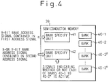
- Figure 4 shows a principle of a semiconductor memory according to the present invention.
- This memory has a function of selecting a required memory cell in a required bank according to first and second address signals successively provided thereto.
- reference numeral 39 denotes the semiconductor memory
- 40-1, 40-2, 40-2 y , and 40-2 x denote banks that maintain an active state even under an unselected state after a write or read operation
- 41 and 42 denote bank specify units for specifying a bank to be selected.
- the x is an integer equal to or greater than two
- the y is an integer equal to or greater than one and is provided by dividing the x by a multiple of two.
- the bank specify unit 41 decodes an x-bit bank address signal contained in the first address signal, to specify one of the 2 x banks functioning as they are or as 2 y banks, so that a word line is selected in the specified bank.
- the bank specify unit 42 decodes, according to information signals indicating whether or not each of the 2 x banks 40-1 to 40-2 x is active, an x-bit bank address signal contained in the second address signal if the 2 x banks function as they are or a y-bit bank address signal contained in the second address signal if the 2 x banks function as 2 y banks, to specify the bank that has been specified according to the first address signal, so that data are written into or read out of the specified bank.
- the present invention employs the bank specify unit 41 for specifying a bank in which a word line is selected and the bank specify unit 42 for specifying the bank that has been specified according to the first address signal, so that data are written into or read out of the specified bank.
- the bank specify unit 42 decodes, according to information signals indicating whether or not each of the 2 x banks 40-1 to 40-2 x is active, an x-bit bank address signal contained in the second address signal if the 2 x banks function as they are or a y-bit bank address signal contained in the second address signal if the 2 x banks function as 2 y banks, to specify the bank that has been specified according to the first address signal, so that data are written into or read out of the specified bank.
- this semiconductor memory also serves as a 2 y -bank memory so that it is applicable not only to the computer systems employing 2 x -bank memories but also to the computer systems employing 2 y -bank memories.
- Figures 5A and 5B show parts of a four-bank SDRAM according to an embodiment of the present invention.
- this embodiment is different from the SDRAM of the prior art shown in Figs. 1A and 1B that this embodiment of Figs. 5A and 5B has drivers 44 to 47 for providing bank status signals S1 to S4 to indicate whether or not each bank is active, instead of the drivers 19 to 22 of the prior art.
- the SDRAM of the embodiment according to the present invention has a bank decoder 48 in addition to the prior art SDRAM shown in Figs. 1A and 1B.
- the bank decoder 48 of the present embodiment is used to decode a bank address provided by a bank address buffer 17 according to the bank status signals S1 to S4 which are provided by the drivers 44 to 47.
- the SDRAM of this embodiment shown in Figs. 5A and 5B has selectors 25, 34, and 37 in addition to the prior art SDRAM shown in Figs. 1A and 1B.
- the selectors 25, 34, and 37 are used to select a bank according to an output of the bank decoder 48.
- the other arrangements of the SDRAM of this embodiment shown in Figs. 5A and 5B are the same as those of the prior art SDRAM shown in Figs. 1A and 1B.
- Figure 6 shows a bank decoder of the semiconductor memory shown in Figs. 5A and 5B.
- reference marks BK1 to BK4 denote decoded signals provided by the bank decoder 48.
- Table 1 shows relationships between the decoded signals BK1 to BK4 and banks to be specified.
- Table 1 BK1 BK2 BK3 BK4 Selection Specified Bank H L L L BANK 1 L H L L BANK 2 L L H L BANK 3 L L L H BANK 4
- a reference numeral 50 denotes a section to produce the decoded signal BK1
- 51 to 55 denote P-channel type MOS (pMOS) transistors
- 56 to 60 denote N-channel type MOS (nMOS) transistors
- 61 and 62 denote inverters.
- reference numeral 63 denotes a section to produce the decoded signal BK2
- 64 to 68 denote pMOS transistors
- 69 to 73 denote nMOS transistors
- 74 and 75 denote inverters
- reference numeral 76 denotes a section to produce the decoded signal BK3, 77 to 81 denote pMOS transistors
- 82 to 86 denote nMOS transistors
- 87 and 88 denote inverters
- 89 denotes a section to produce the decoded signal BK4
- 90 to 94 are pMOS transistors, 95 to 99 denote nMOS transistors, and 100 and 101 denote inverters.
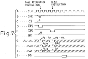
- Figure 7 is a timechart showing a read operation of the semiconductor memory shown in Figs. 5A and 5B, when the semiconductor memory is used as a four-bank memory.
- a reference mark A represents the clock signal CLK
- B clock enable signal CKE
- C chip select signal /CS
- D the row address strobe signal /RAS
- E the column address strobe signal /CAS
- F the write enable signal /WE.
- a reference mark G represents an address signal of bits A0 to An
- H the bit BA0 of a bank address signal
- I the bit BA1 of the bank address signal
- J output data DQ.
- a bank activation instruction and a row address signal are firstly provided.
- the bank activation instruction is provided with the clock enable signal CKE of high (high level “H"), chip select signal /CS of low (low level “L”), row address strobe signal /RAS of "L”, column address strobe signal /CAS of "H", and write enable signal /WE of "H”.
- the row address signal involves bits A0 to An+2 among which the bits An+1 and An+2 are latched as the bits BA0 and BA1 of a bank address signal by the bank address buffer 17, and the bits A0 to An are latched by the address buffer 23.
- the bank address signal of bits BA0 and BA1 latched by the bank address buffer 17 becomes a complementary signal, which is transferred to the bank decoders 18 and 48. In this case, the bank decoder 48 is controlled to ignore the bank address signal.
- the bank address signal of bits BA0 and BA1 is decoded by the bank decoder 18, and the decoded signal is supplied to the drivers 44 to 47 and selector 24.
- One of the drivers 44 to 47 selected by the decoded signal drives the corresponding word decoder and sense amplifier to activate the corresponding bank, which becomes ready to provide data.
- the bits A0 to An of the row address signal latched by the address buffer 23 are transferred to the word decoder of the selected bank through the selector 24, so that a word line is selected in the bank.
- a read instruction is then issued.
- the read instruction is provided with the clock enable signal CKE of "H”, chip select signal /CS of "L”, row address strobe signal /RAS of "H”, column address strobe signal /CAS of "L”, and write enable signal /WE of "H”.
- a bank address signal of bits BA0 and BA1 and a column address signal of bits A0 to An are received.
- the bank address signal of bits BA0 and BA1 is latched by the bank address buffer 17, and the column address signal of bits A0 to An is latched by the address buffer 23.
- the bank address signal of bits BA0 and BA1 latched by the bank address buffer 17 becomes a complementary signal, which is transferred to the bank decoders 18 and 48. At this time, the bank decoder 18 is controlled to ignore the bank address signal, and the bank decoder 48 decodes the bank address signal.
- Tables 2 to 5 show functions of the bank decoder 48 when the embodiment serves as a four-bank memory.
- Table 2 BA0 BA1 S1 S2 S3 S4 BK1 BK2 BK3 BK4 L L H L L L H L L L L L L H H L L H L L L L L L H L H L H L L L L L L H L H L H L L L L L L H L L H H L L L L L L H H H L H L L L L L L H H H L H L L L L L L H H H H L L L L L L H H H H H H L L L L L L L H H H H H H L L L L L L H H H H H H L L L L L L L H H H H H H L L L L L L L H H H H H H L L L L L L L H H H H H H L L L L L L L L H H H H H H L L L L L L L
- the bank decoder 48 provides a decoded signal of bits BK1 of "H”, BK2 of "L”, BK3 of "L” and BK4 of "L", to correctly specify the bank 1 to be selected.
- Table 3 BA0 BA1 S1 S2 S3 S4 BK1 BK2 BK3 BK4 H L L H L L L H L H H L L L H L L H L L H L L H L L H L L H L H L H L H L H L H L H L H L H L H L H L H L H L H L H L H L H L H L H L H L H L H L H L H L H L H L H L H L H L H L H L H L H L H L H L H L H L H L H L H L H L H H H H H L H L H L H L H L H L H H H H H L H L L L H L H H H H H L H L L L H L H H H H H L H L L L L H H H H H H L H L L
- the bank decoder 48 provides a decoded signal of bits BK1 of "L”, BK2 of "L”, BK3 of "H", and BK4 of "L", to correctly specify the bank 3 to be selected.
- Table 5 BA0 BA1 S1 S2 S3 S4 BK1 BK2 BK3 BK4 H H L L L L H L H H H H L L H L L L L H H H H L H L H L L L L H H H H L L L L L H H H H H L H L L L L H H H H H L H L L L L H H H H H L H L L L H H H H H H H H L L L L H H H H H H H H L L L L H H H H H H H H L L L H H H H H H H L L L H H H H H H H L L L H H H H H H H L L L H H H H H H H L L L H H H H H H H L L L H H H H H H L L L H H H H H H
- the column address signal of bits A0 to An latched by the address buffer 23 is supplied to the column decoder of the selected bank through the selector 25, so that a column is selected in the bank.
- Data read out of the selected bank are latched by the output buffer 35 through the sense amplifier and amplifier of the selected bank and the selector 34 and are provided outside. In this way, the SDRAM of this embodiment serving as the four-bank memory completes the read operation.
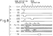
- Figure 8 is a timechart showing a read operation of the semiconductor memory shown in Figs. 5A and 5B, when the semiconductor memory is used as a two-bank memory with the banks 1 and 2 serving as a bank and the banks 3 and 4 as another bank.
- the reference marks of the signals are the same as that shown in Fig. 7.
- a computer system employing the two-bank SDRAM issues a bank activation instruction and row address signal.
- the bank activation instruction is provided with the clock enable signal CKE of "H”, chip select signal /CS of "L”, row address strobe signal /RAS of "L”, column address strobe signal /CAS of "H", and write enable signal /WE of "H”.
- the row address signal involves bits A0 to An+2.
- the bits An+1 and An+2 serve as bits BA0 and BA1 of a bank address signal, which are latched by the bank address buffer 17.
- the remaining bits A0 to An are latched by the address buffer 23.
- the bank address signal of bits BA0 and BA1 latched by the bank address buffer 17 becomes a complementary signal, which is transferred to the bank decoders 18 and 48. In this case, the bank decoder 48 is controlled to ignore the bank address signal.
- the bank decoder 18 decodes the bank address signal of bits BA0 and BA1 and provides the decoded signal to the drivers 44 to 47 and selector 24.
- One of the drivers 44 to 47 specified by the decoded signal drives the word decoder and sense amplifier of the corresponding bank, to make the bank ready to be read.
- the bits A0 to An of the row address signal latched by the address buffer 23 are transferred to the word decoder of the selected bank through the selector 24, so that a word line is selected in the bank.
- a read instruction is then provided with the clock enable signal CKE of "H", chip select signal /CS of "L”, row address strobe signal /RAS of "H", column address strobe signal /CAS of "L”, and write enable signal /WE of "H".
- a bank address signal of bit BA1 and a column address signal of bits A0 to An with no bit An+1 are provided.
- the bank address signal bit BA1 is latched by the bank address buffer 17.
- the column address signal of bits A0 to An is latched by the address buffer 23.
- the bank address signal BA1 latched by the bank address buffer 17 becomes a complementary signal, which is transferred to the bank decoders 18 and 48. In this case, the bank decoder 18 is controlled to ignore the bank address signal.
- the bank decoder 48 decodes the bank address signal BA1 and supplies a decoded signal of bits BK1 to BK4 to the selectors 25, 34, and 37.
- the selector 37 is controlled to ignore the decoded signal.
- Table 6 shows functions of the bank decoder 48 when the embodiment serves as a two-bank memory with the banks 1 and 2 functioning as one bank and the banks 3 and 4 as another bank.
- a mark X may take any one of "H" and "L”.
- the bank 2 is activated. Thereafter, if the bank address signal BA1 issued with the read instruction and the column address signal of bits A0 to An is "L", not only the bank 2 but also any one of the banks 3 and 4 will be active as shown in Table 6. Under this situation, the bank decoder 48 provides a decoded signal of bits BK1 of "L”, BK2 of "H”, BK3 of "L", and BK4 of "L", to correctly specify the bank 2 to be selected.
- the bank 4 is activated. Thereafter, if the bank address signal BA1 issued with the read instruction and the column address signal of bits A0 to An is "H", not only the bank 4 but also any one of the banks 1 and 2 will be active as shown in Table 6. Under this situation, the bank decoder 48 provides a decoded signal of bits BK1 of "L”, BK2 of "L”, BK3 of "L", and BK4 of "H", to correctly specify the bank 4 to be selected.
- the column address signal of bits A0 to An latched by the address buffer 23 is supplied to the column decoder of the selected bank through the selector 25, so that a column is selected in the selected bank.
- Data read out of the selected bank are latched by the output buffer 35 through the sense amplifier and amplifier of the selected bank and the selector 34 and are provided outside. In this way, the SDRAM of this embodiment serving as the two-bank memory completes the read operation.
- the selector 37 instead of the selector 34 works, and the SDRAM serves as any one of the four- and two-bank memories similar to the read operation.
- this embodiment employs the bank decoder 18 for decoding a bank address signal of bits BA0 and BA1 contained in a row address signal of bits A0 to An+1, to specify a bank in which a word line is selected.
- the embodiment also employs the bank decoder 48 for specifying the bank specified according to the bank address signal of bits BA0 and BA1 contained in the row address signal of bits A0 to An+1 so that data are read out of or written into the specified bank, according to bank status signals S1 to S3 that indicate whether or not each of the banks 1 to 4 is active. Accordingly, this embodiment serves not only as a four-bank memory but also as a two-bank memory, to secure improved convenience.
- an embodiment of the invention provides a semiconductor memory having a bank specify unit (41) for specifying a bank in which a word line is selected according to a bank address signal contained in a first address signal, and a bank specify unit (42) for specifying the bank selected according to the first address signal according to signals that indicate whether or not each of the banks (40-1, 40-2, ..., 40-2 x ) is active and a bank address signal contained in a second address signal that is provided after the first address signal, so that data are read out of or written into the specified bank.
- the semiconductor memory of the present invention is capable of serving as a memory having a smaller number of banks, to thereby improve convenience.
Landscapes
- Engineering & Computer Science (AREA)
- Microelectronics & Electronic Packaging (AREA)
- Theoretical Computer Science (AREA)
- Physics & Mathematics (AREA)
- General Engineering & Computer Science (AREA)
- General Physics & Mathematics (AREA)
- Computer Hardware Design (AREA)
- Dram (AREA)
- Static Random-Access Memory (AREA)
Abstract
Description
- The present invention relates to a semiconductor memory, and more particularly, to a semiconductor memory having a plurality of memory cell areas called banks.
- Recently, a synchronous dynamic random access memory (SDRAM) has been provided and used for a computer system, and the like. Further, a SDRAM having a plurality of banks (for example, two banks, four banks, or eight banks) has been studied and also provided. Note that the banks are maintained in an active state if required even under an unselected state.
- For example, in a SDRAM having two banks, when one bank carries out an active operation, the other bank simultaneously carries out a precharge operation, so that the total operation speed becomes high. Further, for example, a SDRAM having a plurality of banks is used for a cache memory of a computer system, so as to accelerate the cache operation thereof.
- Note that, among computer systems, some are designed to use four-bank SDRAMs and some are designed to use two-bank SDRAMs. In these four-bank and two-bank SDRAMs used as the cache memory of the computer system, the configuration of the SDRAM, i.e., the number of the banks, is determined in accordance with the requirement of the computer system, or the configuration of the computer system using the SDRAM.
- Nevertheless, in the prior art SDRAM having a plurality of banks, for example, the four-bank SDRAM of the prior art is incompatible with the two-bank SDRAM, so that it is not applicable to the computer systems that operate with two-bank SDRAMs. This problem of prior art SDRAMs will be explained in detail with reference to the accompanying drawing.
- An embodiment of the present invention may provide a semiconductor memory having a plurality of banks and able to serve as a memory having a smaller number of banks.
- According to the present invention, there is provided a semiconductor memory comprising a plurality of banks, each of the banks having a plurality of memory cells, and a specific memory cell of a specific bank being selected in accordance with a first address signal and a second address signal successively provided to the semiconductor memory; a first specify unit for specifying one of the plurality of banks by decoding a bank address signal contained in the first address signal; and a second specify unit for specifying one of the plurality of banks by decoding the bank address signal contained in the first address signal, according to bank status signals that indicates whether or not each of the banks is activated, so that the semiconductor memory is used for different bank configurations.
- The semiconductor memory may be a dynamic random access memory, or a synchronous dynamic random access memory. In this synchronous dynamic random access memory, a bank activation instruction and a read instruction may be provided with a clock enable signal, a chip select signal, a row address strobe signal, a column address strobe signal, and a write enable signal.
- The semiconductor memory may further comprise a plurality of drivers for driving corresponding word decoders and sense amplifiers, and the bank status signals may be output from the drivers. The banks may maintain an active state if required even under an unselected state after a read operation or a write operation. The first address signal may be a row address signal, and the second address signal may be a column address signal.
- The number of the banks may be determined as 2x, where x being an integer equal to or greater than two; the bank configurations may include a first bank configuration and a second bank configuration, the first bank configuration being 2x and the second bank configuration being 2y, where y being an integer equal to or greater than one and obtained by dividing the x by a multiple of two. The first specify unit may decode an x-bit bank address signal contained in the first address signal, to specify one of the 2x banks functioning as they are or as 2y banks; and the second specify unit may decode, according to information signals indicating whether or not each of the 2x banks is active, an x-bit bank address signal contained in the second address signal if the 2x banks function as they are or a y-bit bank address signal contained in the second address signal if the 2x banks function as 2y banks, to specify the bank that has been specified according to the first address signal, so that data are written into or read out of the specified bank.
- Further, according to the present invention, there is also provided a semiconductor memory having 2x banks, where x being an integer equal to or greater than two, that maintain an active state if required even under an unselected state after a read or write operation, any memory cell in any one of the banks being selectable according to a first address signal and a second address signal successively provided to the semiconductor memory, wherein the semiconductor memory comprises a first specify unit for decoding an x-bit bank address signal contained in the first address signal, to specify one of the 2x banks functioning as they are or as 2y banks, where y being an integer equal to or greater than one and obtained by dividing the x by a multiple of two, so that a word line is selected in the specified bank; and a second specify unit for decoding, according to information signals indicating whether or not each of the 2x banks is active, an x-bit bank address signal contained in the second address signal if the 2x banks function as they are or a y-bit bank address signal contained in the second address signal if the 2x banks function as 2y banks, to specify the bank that has been specified according to the first address signal, so that data are written into or read out of the specified bank.
- The present invention will be more clearly understood from the description of the preferred embodiments as set forth below with reference to the accompanying drawings, wherein:
- Figs. 1A and 1B are block diagrams showing parts of a semiconductor memory according to the prior art;
- Fig. 2 is a timechart showing a read operation of the semiconductor memory shown in Figs. 1A and 1B;
- Fig. 3 is a timechart for explaining the problems caused in the semiconductor memory shown in Figs. 1A and 1B;
- Fig. 4 is a block diagram showing a principle of a semiconductor memory according to the present invention;
- Figs. 5A and 5B are block diagrams showing parts of an embodiment of a semiconductor memory according to the present invention;
- Fig. 6 is a circuit diagram showing a bank decoder of the semiconductor memory shown in Figs. 5A and 5B;
- Fig. 7 is a timechart showing a read operation of the semiconductor memory shown in Figs. 5A and 5B, when the semiconductor memory is used as a four-bank memory; and
- Fig. 8 is a timechart showing a read operation of the semiconductor memory shown in Figs. 5A and 5B, when the semiconductor memory is used as a two-bank memory.
- For a better understanding of the preferred embodiments, the problems of the prior art will be explained, with reference to Figs. 1A to 3.
- Figures 1A and 1B show parts of a semiconductor memory (SDRAM: synchronous dynamic random access memory )according to the prior art. Note that this semiconductor memory is a four-bank SDRAM employing four banks to operate in synchronism with external clock signals.
- In Figs. 1A and 1B,
reference numerals 1 to 4 denote memory cell areas, i.e., banks that maintain an active state if required even under an unselected state after a write or read operation, and 5 to 8 denote word decoders provided for corresponding banks, respectively, to decode an address signal to specify a word line in the banks. - In Figs. 1A and 1B,
reference numerals 9 to 12 denotes sense amplifiers, 13 to 16 denotes column decoders, 17 denotes a bank address buffer, 18 denotes a bank decoder, and 19 to 22 denotes drivers. Further,reference numeral 23 denotes an address buffer, 24 denotes a selector, and 25 denotes a selector. - The
column decoders 13 to 16 are used to decode a column address signal for specifying a column in thebanks 1 to 4, and thesense amplifiers 9 to 12 are used to amplify data read out from thebanks 1 to 4. Thebank address buffer 17 is used to receive a bank address signal of bits BA0 and BA1 for selecting one of thebanks 1 to 4, and thebank decoder 18 is used to decode the bank address signal. - One of the
drivers 19 to 22 is activated to drive the word decoder and sense amplifier of a selected bank, according to the decoded signal provided by thebank decoder 18. Theaddress buffer 23 is used to receive an address signal of bits A0 to An, and theselector 24 is used to supply a word line selecting address signal (which is provided by the address buffer 23) to the word decoder of the bank specified by the decoded signal from thebank decoder 18. - The
selector 25 is used to supply a column address signal provided by theaddress buffer 23 to the column decoder of the bank specified by the decoded signal from thebank decoder 18. - Further, in Figs. 1A and 1B,
reference numerals 26 to 29 denotes amplifiers, 30 to 33 denotes write circuits, 34 denotes a selector. In addition,reference numeral 35 denotes an output buffer, 36 denotes an input buffer, 37 denotes a selector, 37 denotes a selector, and 38 denotes an operation controller. Further, reference mark CLK denotes a clock signal, /RAS denotes a row address strobe signal, /CAS denotes a column address strobe signal, /WE denotes a write enable signal, /CS denotes a chip select signal, and CKE denotes a clock enable signal. Note that, the mark "/" indicates a low enable signal or a low active signal, and thus, for example, the chip select signal /CS is at a low level "L", the chip being supplied with the chip select signal /CS of "L" is selected. - The
amplifiers 26 to 29 are used to amplify data read through thesense amplifiers 9 to 12, and thewrite circuits 30 to 33 are used to write data into thebanks 1 to 4. Theselector 34 is used to select one of theamplifiers 26 to 29 of the bank specified by the decoded signal from thebank decoder 18. - The
output buffer 35 is used to latch data from theselector 34 and provide the same outside, and theinput buffer 36 is used to store write data provided from the outside. Theselector 37 is used to supply the write data from theinput buffer 36 to one of thewrite circuits 30 to 33 of the bank specified by the decoded signal from thebank decoder 18. - The
operation controller 38 is used to control the operation timing of the elements mentioned above according to external control signals, and the clock enable signal CKE is used to enable the clock signal CLK. - Figure 2 is a timechart showing a read operation of the semiconductor memory (SDRAM) shown in Figs. 1A and 1B. In Fig. 2, a reference mark A represents the clock signal CLK, B the clock enable signal CKE, C the chip select signal /CS, D the row address strobe signal /RAS, E the column address strobe signal /CAS, and F the write enable signal /WE. Further, a reference mark G represents an address signal of bits A0 to An, H the bit BA0 of a bank address signal, I the bit BA1 of the bank address signal, and J output data DQ.
- The SDRAM latches the externally supplied signals in response to a rise of the clock signal CLK. In a read operation, the SDRAM firstly receives a bank activation instruction and row address signal. The bank activation instruction is provided with the clock enable signal CKE of a high level "H", chip select signal /CS of a low level "L", row address strobe signal /RAS of the low level "L", column address strobe signal /CAS of the high level "H", and write enable signal /WE of the high level "H".
- The row address signal involves bits A0 to An+2. The bits An+1 and An+2 are latched as the bits BA0 and BA1 of the bank address signal by the
bank address buffer 17, and the bits A0 to An are latched by theaddress buffer 23. The bank address signal of bits BA0 and BA1 latched by thebank address buffer 17 are changed to complementary signals, and the complementary signals are supplied to thebank decoder 18 and decoded therein. The decoded signals are supplied to thedrivers 19 to 22 andselectors selectors - One of the
drivers 19 to 22 corresponding to the decoded signal activates the corresponding word decoder and sense amplifier, to make the corresponding bank ready to be read. The bits A0 to An of the row address signal latched by theaddress buffer 23 are transferred to one of theword decoders 5 to 8 corresponding to the selected bank through theselector 24, so that a word line is selected in the bank. - The SDRAM then receives a read instruction. The read instruction is provided with the clock enable signal CKE of "H", chip selector signal /CS of "L", row address strobe signal /RAS of "H", column address strobe signal /CAS of "L", and write enable signal /WE of "H".
- A bank address signal of bits BA0 and BA1 is latched by the
bank address buffer 17, and a column address signal of bits A0 to An is latched by theaddress buffer 23. - The bank address signal of bits BA0 and BA1 latched by the
bank address buffer 17 becomes a complementary signal, which is decoded by thebank decoder 18. The decoded signal is supplied to thedrivers 19 to 22 andselectors drivers 19 to 22 andselectors - The column address signal of bits A0 to An latched by the
address buffer 23 is supplied to the column decoder (13) of the selected bank (for example, bank 1) through theselector 25, so that a column is selected in the bank (1). Then, data are read out of the selected bank (1) and are latched by theoutput buffer 35 through the corresponding sense amplifier (9) and amplifier (26) and theselector 34. Theoutput buffer 35 provides the data DQ outside. - By the way, among computer systems, some are designed to use four-bank SDRAMs and some are designed to use two-bank SDRAMs. Note that these four-bank and two-bank SDRAMs may be used as a cache memory of a computer system, and the configuration of the SDRAM (for example, the number of the banks) is determined in accordance with the requirement of the computer system, or the configuration of the computer system using the SDRAM. Note that the four-bank memory shown in Figs. 1A and 1B is not usable as a two-bank memory, and this is, therefore, inconvenient.
- Figure 3 is a timechart for explaining the problems caused in the semiconductor memory shown in Figs. 1A and 1B. In Fig. 3, the reference marks of the signals are the same as that shown in Fig. 2.
- As shown in Fig. 3, in a read operation, the computer system designed to employ two-bank SDRAMs firstly issues a bank activation instruction and row address signal to the SDRAM.
- The bank activation instruction is provided with the clock enable signal CKE of a high level "H", chip select signal /CS of a low level "L", row address strobe signal /RAS of "L", column address strobe signal /CAS of "H", and write enable signal /WE of "H". The row address signal involves bits A0 to An+2. The bits An+1 and An+2 serve as the bits BA0 and BA1 of a bank address signal, which is latched by the
bank address buffer 17. The remaining bits A0 to An are latched by theaddress buffer 23. - The bank address signal of bits BA0 and BA1 latched by the
bank address buffer 17 becomes a complementary signal, which is decoded by thebank decoder 18. The decoded signal is supplied to thedrivers 19 to 22 andselectors selectors drivers 19 to 22 specified by the decoded signal drives the corresponding word decoder and sense amplifier, to thereby activate the corresponding bank and make the bank ready to be read. - The bits A0 to An of the row address signal latched by the
address buffer 23 are transferred to one of the word decoders corresponding to the selected bank through theselector 24, so that a word line is selected in the bank. - The SDRAM then receives a read instruction. The read instruction is provided with the clock enable signal CKE of "H", chip select signal /CS of "L", row address strobe signal /RAS of "H", column address strobe signal /CAS of "L", and write enable signal /WE of "H". In this case, the address signal bit An+1 is not supplied. Instead, a bank address signal of bit BA1 and a column address signal of bits A0 to An are supplied. The bank address signal is latched by the
bank address buffer 17 and is decoded by thebank decoder 18. - For example, the
bank 1 is selected with a bank address signal of bits BA0 of "L" and BA1 of "L", and thebank 2 with a bank address signal of bits BA0 of "H" and BA1 of "L", thebank 3 with a bank address signal of bits BA0 of "L" and BA1 of "H", and thebank 4 with a bank address signal of bits BA0 of "H" and BA1 of "H". - If the
bank 1 is activated with a bank activation instruction involving the bank address signal of bits BA0 of "L" and BA1 of "L" while thebank 2 is active, thebank 1 will be selected for a read operation only when a read instruction is provided with the bank address signal of bits BA0 of "L" and BA1 of "L" in addition to a column address signal of bits A0 to An. Further, if the bit BA1 is "L" and the bit BA0 is indefinite, for example, "H", thebank 2 will be selected instead of thebank 1. Then, erroneous data will be read. - The computer system employing the two-bank SDRAMs issues a read instruction with a column address signal of bits A0 to An and a bank selection signal of only bit BA1, so that the
selector 34 is unable to correctly select a bank. This is also true in a write operation. Namely, theselector 37 is unable to select a correct bank, and the data will be written into a wrong bank. - In this way, the four-bank SDRAM of the prior art shown in Figs. 1A and 1B is incompatible with a two-bank SDRAM, so that it is not applicable to the computer systems that operate with two-bank SDRAMs.
- Below, an embodiment of a semiconductor memory according to the present invention will be explained with reference to Figs. 4 to 8.
- Figure 4 shows a principle of a semiconductor memory according to the present invention. This memory has a function of selecting a required memory cell in a required bank according to first and second address signals successively provided thereto.
- In Fig. 4,
reference numeral 39 denotes the semiconductor memory, 40-1, 40-2, 40-2y, and 40-2x denote banks that maintain an active state even under an unselected state after a write or read operation, and 41 and 42 denote bank specify units for specifying a bank to be selected. Note that the x is an integer equal to or greater than two, and the y is an integer equal to or greater than one and is provided by dividing the x by a multiple of two. - The bank specify
unit 41 decodes an x-bit bank address signal contained in the first address signal, to specify one of the 2x banks functioning as they are or as 2y banks, so that a word line is selected in the specified bank. The bank specifyunit 42 decodes, according to information signals indicating whether or not each of the 2x banks 40-1 to 40-2x is active, an x-bit bank address signal contained in the second address signal if the 2x banks function as they are or a y-bit bank address signal contained in the second address signal if the 2x banks function as 2y banks, to specify the bank that has been specified according to the first address signal, so that data are written into or read out of the specified bank. - As described above, the present invention employs the bank specify
unit 41 for specifying a bank in which a word line is selected and the bank specifyunit 42 for specifying the bank that has been specified according to the first address signal, so that data are written into or read out of the specified bank. - The bank specify
unit 42 decodes, according to information signals indicating whether or not each of the 2x banks 40-1 to 40-2x is active, an x-bit bank address signal contained in the second address signal if the 2x banks function as they are or a y-bit bank address signal contained in the second address signal if the 2x banks function as 2y banks, to specify the bank that has been specified according to the first address signal, so that data are written into or read out of the specified bank. In this way, this semiconductor memory also serves as a 2y-bank memory so that it is applicable not only to the computer systems employing 2x-bank memories but also to the computer systems employing 2y-bank memories. - Figures 5A and 5B show parts of a four-bank SDRAM according to an embodiment of the present invention. By comparing Figs. 5A and 5B with Figs. 1A and 1B, this embodiment is different from the SDRAM of the prior art shown in Figs. 1A and 1B that this embodiment of Figs. 5A and 5B has
drivers 44 to 47 for providing bank status signals S1 to S4 to indicate whether or not each bank is active, instead of thedrivers 19 to 22 of the prior art. - When a
word decoder 5 andsense amplifier 9 are driven to activate abank 1, the bank status signal S1 becomes high (high level "H"), and when theword decoder 5 andsense amplifier 9 are put off to deactivate thebank 1, the bank status signal S1 becomes low (low level "L"). Similarly, when aword decoder 6 andsense amplifier 10 are driven to activate abank 2, the bank status signal S2 becomes "H", and when theword decoder 6 andsense amplifier 10 are put off to deactivate thebank 2, the bank status signal S2 becomes "L". - Further, when a
word decoder 7 andsense amplifier 11 are driven to activate abank 3, the bank status signal S3 becomes "H", and when theword decoder 7 andsense amplifier 11 are put off to deactivate thebank 3, the bank status signal S3 becomes "L". Similarly, when a word decoder 8 and sense amplifier 12 are driven to activate abank 4, the bank status signal S4 becomes "H", and when the word decoder 8 and sense amplifier 12 are put off to deactivate thebank 4, the bank status signal S4 becomes "L". - Next, as shown in Fig. 5A and 5B, the SDRAM of the embodiment according to the present invention has a
bank decoder 48 in addition to the prior art SDRAM shown in Figs. 1A and 1B. Thebank decoder 48 of the present embodiment is used to decode a bank address provided by abank address buffer 17 according to the bank status signals S1 to S4 which are provided by thedrivers 44 to 47. Further, the SDRAM of this embodiment shown in Figs. 5A and 5B hasselectors selectors bank decoder 48. Note that the other arrangements of the SDRAM of this embodiment shown in Figs. 5A and 5B are the same as those of the prior art SDRAM shown in Figs. 1A and 1B. - Figure 6 shows a bank decoder of the semiconductor memory shown in Figs. 5A and 5B. In Fig. 6, reference marks BK1 to BK4 denote decoded signals provided by the
bank decoder 48. Table 1 shows relationships between the decoded signals BK1 to BK4 and banks to be specified.Table 1 BK1 BK2 BK3 BK4 Selection Specified Bank H L L L BANK 1 L H L L BANK 2 L L H L BANK 3 L L L H BANK 4 - In Fig. 6, a
reference numeral 50 denotes a section to produce the decoded signal BK1, 51 to 55 denote P-channel type MOS (pMOS) transistors, 56 to 60 denote N-channel type MOS (nMOS) transistors, and 61 and 62 denote inverters. - Further,
reference numeral 63 denotes a section to produce the decoded signal BK2, 64 to 68 denote pMOS transistors, 69 to 73 denote nMOS transistors, and 74 and 75 denote inverters. In addition,reference numeral 76 denotes a section to produce the decoded signal BK3, 77 to 81 denote pMOS transistors, 82 to 86 denote nMOS transistors, 87 and 88 denote inverters, 89 denotes a section to produce the decoded signal BK4, 90 to 94 are pMOS transistors, 95 to 99 denote nMOS transistors, and 100 and 101 denote inverters. - Figure 7 is a timechart showing a read operation of the semiconductor memory shown in Figs. 5A and 5B, when the semiconductor memory is used as a four-bank memory.
- In Fig. 7, a reference mark A represents the clock signal CLK, B the clock enable signal CKE, C the chip select signal /CS, D the row address strobe signal /RAS, E the column address strobe signal /CAS, and F the write enable signal /WE. Further, a reference mark G represents an address signal of bits A0 to An, H the bit BA0 of a bank address signal, I the bit BA1 of the bank address signal, and J output data DQ.
- These externally supplied signals are latched in response to a rise of the clock signal CLK. In a read operation, a bank activation instruction and a row address signal are firstly provided. The bank activation instruction is provided with the clock enable signal CKE of high (high level "H"), chip select signal /CS of low (low level "L"), row address strobe signal /RAS of "L", column address strobe signal /CAS of "H", and write enable signal /WE of "H".
- The row address signal involves bits A0 to An+2 among which the bits An+1 and An+2 are latched as the bits BA0 and BA1 of a bank address signal by the
bank address buffer 17, and the bits A0 to An are latched by theaddress buffer 23. - The bank address signal of bits BA0 and BA1 latched by the
bank address buffer 17 becomes a complementary signal, which is transferred to thebank decoders bank decoder 48 is controlled to ignore the bank address signal. The bank address signal of bits BA0 and BA1 is decoded by thebank decoder 18, and the decoded signal is supplied to thedrivers 44 to 47 andselector 24. - One of the
drivers 44 to 47 selected by the decoded signal drives the corresponding word decoder and sense amplifier to activate the corresponding bank, which becomes ready to provide data. - The bits A0 to An of the row address signal latched by the
address buffer 23 are transferred to the word decoder of the selected bank through theselector 24, so that a word line is selected in the bank. - A read instruction is then issued. The read instruction is provided with the clock enable signal CKE of "H", chip select signal /CS of "L", row address strobe signal /RAS of "H", column address strobe signal /CAS of "L", and write enable signal /WE of "H".
- A bank address signal of bits BA0 and BA1 and a column address signal of bits A0 to An are received. The bank address signal of bits BA0 and BA1 is latched by the
bank address buffer 17, and the column address signal of bits A0 to An is latched by theaddress buffer 23. - The bank address signal of bits BA0 and BA1 latched by the
bank address buffer 17 becomes a complementary signal, which is transferred to thebank decoders bank decoder 18 is controlled to ignore the bank address signal, and thebank decoder 48 decodes the bank address signal. - Tables 2 to 5 show functions of the
bank decoder 48 when the embodiment serves as a four-bank memory.Table 2 BA0 BA1 S1 S2 S3 S4 BK1 BK2 BK3 BK4 L L H L L L H L L L L L H H L L H L L L L L H L H L H L L L L L H L L H H L L L L L H H H L H L L L L L H H L H H L L L L L H L H H H L L L L L H H H H H L L L - As shown in the above Table 2, if the bits An+1 (the bit BA0 of the bank address signal) and An+2 (the bit BA1 of the bank address signal) of the row address signal issued with the bank activation instruction are "L" and "L", respectively, the
bank 1 is activated. Thereafter, if the bits BA0 and BA1 of the bank address signal issued with the read instruction and the column address signal of bits A0 to An are "L" and "L", respectively, not only thebank 1 but also one, two, or all of thebanks bank decoder 48 provides a decoded signal of bits BK1 of "H", BK2 of "L", BK3 of "L" and BK4 of "L", to correctly specify thebank 1 to be selected.Table 3 BA0 BA1 S1 S2 S3 S4 BK1 BK2 BK3 BK4 H L L H L L L H L L H L H H L L L H L L H L L H H L L H L L H L L H L H L H L L H L H H H L L H L L H L H H L H L H L L H L L H H H L H L L H L H H H H L H L L - As shown in the above Table 3, if the bits An+1 (the bit BA0 of the bank address signal) and An+2 (the bit BA1 of the bank address signal) of the row address signal issued with the bank activation instruction are "H" and "L", respectively, the
bank 2 is activated. Thereafter, if the bits BA0 and BA1 of the bank address signal issued with the read instruction and the column address signal of bits A0 to An are "H" and "L", respectively, not only thebank 2 but also one, two, or all of thebanks bank decoder 48 provides a decoded signal of bits BK1 of "L", BK2 of "H", BK3 of "L", and BK4 of "L", to correctly specify thebank 2 to be selected.Table 4 BA0 BA1 S1 S2 S3 S4 BK1 BK2 BK3 BK4 L H L L H L L L H L L H H L H L L L H L L H L H H L L L H L L H L L H H L L H L L H H H H L L L H L L H H L H H L L H L L H L H H H L L H L L H H H H H L L H L - As shown in the above Table 4, if the bits An+1 (the bit BA0 of the bank address signal) and An+2 (the bit BA1 of the bank address signal) of the row address signal issued with the bank activation instruction are "L" and "H", respectively, the
bank 3 is activated. Thereafter, if the bits BA0 and BA1 of the bank address signal issued with the read instruction and the column address signal of bits A0 to An are "L" and "H", respectively, not only thebank 3 but also one, two, or all of thebanks bank decoder 48 provides a decoded signal of bits BK1 of "L", BK2 of "L", BK3 of "H", and BK4 of "L", to correctly specify thebank 3 to be selected.Table 5 BA0 BA1 S1 S2 S3 S4 BK1 BK2 BK3 BK4 H H L L L H L L L H H H H L L H L L L H H H L H L H L L L H H H L L H H L L L H H H H H L H L L L H H H H L H H L L L H H H L H H H L L L H H H H H H H L L L H - As shown in the above Table 5, if the bits An+1 (the bit BA0 of the bank address signal) and An+2 (the bit BA1 of the bank address signal) of the row address signal issued with the bank activation instruction are "H" and "H", respectively, the
bank 4 is activated. Thereafter, if the bits BA0 and BA1 of the bank address signal issued with the read instruction and the column address signal of bits A0 to An are "H" and "H", respectively, not only thebank 4 but also one, two, or all of thebanks bank decoder 48 provides a decoded signal of bits BK1 of "L", BK2 of "L", BK3 of "L", and BK4 of "H", to correctly specify thebank 4 to be selected. - The column address signal of bits A0 to An latched by the
address buffer 23 is supplied to the column decoder of the selected bank through theselector 25, so that a column is selected in the bank. Data read out of the selected bank are latched by theoutput buffer 35 through the sense amplifier and amplifier of the selected bank and theselector 34 and are provided outside. In this way, the SDRAM of this embodiment serving as the four-bank memory completes the read operation. - Figure 8 is a timechart showing a read operation of the semiconductor memory shown in Figs. 5A and 5B, when the semiconductor memory is used as a two-bank memory with the
banks banks - In the read operation, a computer system employing the two-bank SDRAM issues a bank activation instruction and row address signal.
- The bank activation instruction is provided with the clock enable signal CKE of "H", chip select signal /CS of "L", row address strobe signal /RAS of "L", column address strobe signal /CAS of "H", and write enable signal /WE of "H".
- The row address signal involves bits A0 to An+2. The bits An+1 and An+2 serve as bits BA0 and BA1 of a bank address signal, which are latched by the
bank address buffer 17. The remaining bits A0 to An are latched by theaddress buffer 23. - The bank address signal of bits BA0 and BA1 latched by the
bank address buffer 17 becomes a complementary signal, which is transferred to thebank decoders bank decoder 48 is controlled to ignore the bank address signal. - The
bank decoder 18 decodes the bank address signal of bits BA0 and BA1 and provides the decoded signal to thedrivers 44 to 47 andselector 24. - One of the
drivers 44 to 47 specified by the decoded signal drives the word decoder and sense amplifier of the corresponding bank, to make the bank ready to be read. - The bits A0 to An of the row address signal latched by the
address buffer 23 are transferred to the word decoder of the selected bank through theselector 24, so that a word line is selected in the bank. - A read instruction is then provided with the clock enable signal CKE of "H", chip select signal /CS of "L", row address strobe signal /RAS of "H", column address strobe signal /CAS of "L", and write enable signal /WE of "H".
- This time, a bank address signal of bit BA1 and a column address signal of bits A0 to An with no bit An+1 are provided. The bank address signal bit BA1 is latched by the
bank address buffer 17. The column address signal of bits A0 to An is latched by theaddress buffer 23. - The bank address signal BA1 latched by the
bank address buffer 17 becomes a complementary signal, which is transferred to thebank decoders bank decoder 18 is controlled to ignore the bank address signal. - The
bank decoder 48 decodes the bank address signal BA1 and supplies a decoded signal of bits BK1 to BK4 to theselectors selector 37 is controlled to ignore the decoded signal. - Table 6 shows functions of the
bank decoder 48 when the embodiment serves as a two-bank memory with thebanks banks Table 6 BA0 BA1 S1 S2 S3 S4 BK1 BK2 BK3 BK4 X L H L L L H L L L X L H L H L H L L L X L H H L H H L L L X L L L L L L H L L X L L H H L L H L L X L L L L H L H L L X H L H H L L L H L X H H H H L L L H L X H L H H L L L H L X H L L L H L L L H X H H H L H L L L H X H L L L H L L L H - As shown in the above Table 6, if the bits An+1 (the bit BA0 of the bank address signal) and An+2 (the bit BA1 of the bank address signal) of the row address signal issued with the bank activation instruction are "L" and "L", respectively, the
bank 1 is activated. Thereafter, if the bank address signal BA1 issued with the read instruction and the column address signal of bits A0 to An is "L", not only thebank 1 but also any one of thebanks bank decoder 48 provides a decoded signal of bits BK1 of "H", BK2 of "L", BK3 of "L", and BK4 of "L", to correctly specify thebank 1 to be selected. - Further, if the bits An+1 (the bit BA0 of the bank address signal) and An+2 (the bit BA1 of the bank address signal) of the row address signal issued with the bank activation instruction are "H" and "L", respectively, the
bank 2 is activated. Thereafter, if the bank address signal BA1 issued with the read instruction and the column address signal of bits A0 to An is "L", not only thebank 2 but also any one of thebanks bank decoder 48 provides a decoded signal of bits BK1 of "L", BK2 of "H", BK3 of "L", and BK4 of "L", to correctly specify thebank 2 to be selected. - Further, as shown in the above Table 6, if the bits An+1 (the bit BA0 of the bank address signal) and An+2 (the bit BA1 of the bank address signal) of the row address signal issued with the bank activation instruction are "L" and "H", respectively, the
bank 3 is activated. Thereafter, if the bank address signal BA1 issued with the read instruction and the column address signal of bits A0 to An is "H", not only thebank 3 but also any one of thebanks bank decoder 48 provides a decoded signal of bits BK1 of "L", BK2 of "L", BK3 of "H", and BK4 of "L", to correctly specify thebank 3 to be selected. - In addition, if the bits An+1 (the bit BA0 of the bank address signal) and An+2 (the bit BA1 of the bank address signal) of the row address signal issued with the bank activation instruction are "H" and "H", respectively, the
bank 4 is activated. Thereafter, if the bank address signal BA1 issued with the read instruction and the column address signal of bits A0 to An is "H", not only thebank 4 but also any one of thebanks bank decoder 48 provides a decoded signal of bits BK1 of "L", BK2 of "L", BK3 of "L", and BK4 of "H", to correctly specify thebank 4 to be selected. - The column address signal of bits A0 to An latched by the
address buffer 23 is supplied to the column decoder of the selected bank through theselector 25, so that a column is selected in the selected bank. Data read out of the selected bank are latched by theoutput buffer 35 through the sense amplifier and amplifier of the selected bank and theselector 34 and are provided outside. In this way, the SDRAM of this embodiment serving as the two-bank memory completes the read operation. - In a write operation, the
selector 37 instead of theselector 34 works, and the SDRAM serves as any one of the four- and two-bank memories similar to the read operation. - As explained above, this embodiment employs the
bank decoder 18 for decoding a bank address signal of bits BA0 and BA1 contained in a row address signal of bits A0 to An+1, to specify a bank in which a word line is selected. The embodiment also employs thebank decoder 48 for specifying the bank specified according to the bank address signal of bits BA0 and BA1 contained in the row address signal of bits A0 to An+1 so that data are read out of or written into the specified bank, according to bank status signals S1 to S3 that indicate whether or not each of thebanks 1 to 4 is active. Accordingly, this embodiment serves not only as a four-bank memory but also as a two-bank memory, to secure improved convenience. - Thus, an embodiment of the invention provides a semiconductor memory having a bank specify unit (41) for specifying a bank in which a word line is selected according to a bank address signal contained in a first address signal, and a bank specify unit (42) for specifying the bank selected according to the first address signal according to signals that indicate whether or not each of the banks (40-1, 40-2, ..., 40-2x) is active and a bank address signal contained in a second address signal that is provided after the first address signal, so that data are read out of or written into the specified bank. With this arrangement, the semiconductor memory of the present invention is capable of serving as a memory having a smaller number of banks, to thereby improve convenience.
- Many different embodiments of the present invention may be constructed without departing from the spirit and scope of the present invention, and it should be understood that the present invention is not limited to the specific embodiments described in this specification, except as defined in the appended claims.
Claims (10)
- A semiconductor memory having a plurality of banks (40-1, 40-2, ..., 40-2x, 1 to 4), each of said banks having a plurality of memory cells, and a specific memory cell of a specific bank being selected in accordance with a first address signal (A0 to An+2) and a second address signal (A0 to An+2) provided to said semiconductor memory, characterized in that said semiconductor memory comprises:
a first specify means (41, 18) for specifying one of said plurality of banks by decoding a bank address signal (BA0, BA1; An+1, An+2) contained in said first address signal (A0 to An+2); and
a second specify means (42, 48) for specifying one of said plurality of banks by decoding the bank address signal (BA0, BA1; An+1, An+2) contained in said first address signal (A0 to An+2), according to bank status signals (S1 to S4) that indicates whether or not each of said banks (40-1, 40-2, ..., 40-2x, 1 to 4) is activated, so that said semiconductor memory is used for different bank configurations. - A semiconductor memory as claimed in claim 1, wherein the number of said banks are determined to 2x, where x being an integer equal to or greater than two; said bank configurations include a first bank configuration and a second bank configuration, said first bank configuration being 2x and said second bank configuration being 2y, where y being an integer equal to or greater than one and obtained by dividing the x by a multiple of two.
- A semiconductor memory as claimed in claim 2, wherein said first specify means (41) decodes an x-bit bank address signal contained in said first address signal, to specify one of said 2x banks functioning as they are or as 2y banks; and said second specify means (42) decodes, according to information signals indicating whether or not each of said 2x banks is active, an x-bit bank address signal contained in said second address signal if said 2x banks function as they are or a y-bit bank address signal contained in said second address signal if said 2x banks function as 2y banks, to specify the bank that has been specified according to said first address signal, so that data are written into or read out of said specified bank.
- A semiconductor memory having 2x banks (40-1, 40-2, ..., 40-2x, 1 to 4), where x being an integer equal to or greater than two, that maintain an active state if required even under an unselected state after a read or write operation, any memory cell in any one of said banks being selectable according to a first address signal (A0 to An+2) and a second address signal (A0 to An+2) provided to said semiconductor memory, characterized in that said semiconductor memory comprises:
a first specify means (41, 18) for decoding an x-bit bank address signal contained in said first address signal, to specify one of said 2x banks functioning as they are or as 2y banks, where y being an integer equal to or greater than one and obtained by dividing the x by a multiple of two, so that a word line is selected in said specified bank; and
a second specify means (42, 48) for decoding, according to information signals (S1 to S4) indicating whether or not each of said 2x banks is active, an x-bit bank address signal contained in said second address signal if said 2x banks function as they are or a y-bit bank address signal contained in said second address signal if said 2x banks function as 2y banks, to specify the bank that has been specified according to said first address signal, so that data are written into or read out of said specified bank. - A semiconductor memory as claimed in any one of the preceding claims, wherein said semiconductor memory is a dynamic random access memory (DRAM).
- A semiconductor memory as claimed in claim 5, wherein said dynamic random access memory is a synchronous dynamic random access memory (SDRAM).
- A semiconductor memory as claimed in claim 6, wherein a bank activation instruction and a read instruction are provided with a clock enable signal (CKE), a chip select signal (/CS), a row address strobe signal (/RAS), a column address strobe signal (/CAS), and a write enable signal (/WE).
- A semiconductor memory as claimed in any one of the preceding claims, wherein said semiconductor further memory comprises a plurality of drivers (44 to 47) for driving corresponding word decoders (5 to 8) and sense amplifiers (9 to 12), and said information signals (S1 to S4) are output from said drivers (44 to 47).
- A semiconductor memory as claimed in any one of the preceding claims, wherein said banks maintain an active state if required even under an unselected state after a read operation or a write operation.
- A semiconductor memory as claimed in any one of the preceding claims, wherein said first address signal is a row address signal, and said second address signal is a column address signal.
Applications Claiming Priority (3)
| Application Number | Priority Date | Filing Date | Title |
|---|---|---|---|
| JP208117/93 | 1993-08-24 | ||
| JP20811793 | 1993-08-24 | ||
| JP20811793A JP3304531B2 (en) | 1993-08-24 | 1993-08-24 | Semiconductor storage device |
Publications (3)
| Publication Number | Publication Date |
|---|---|
| EP0640980A2 true EP0640980A2 (en) | 1995-03-01 |
| EP0640980A3 EP0640980A3 (en) | 1995-03-29 |
| EP0640980B1 EP0640980B1 (en) | 2001-10-17 |
Family
ID=16550921
Family Applications (1)
| Application Number | Title | Priority Date | Filing Date |
|---|---|---|---|
| EP94111301A Expired - Lifetime EP0640980B1 (en) | 1993-08-24 | 1994-07-20 | Semiconductor memory having a plurality of banks |
Country Status (5)
| Country | Link |
|---|---|
| US (1) | US5483497A (en) |
| EP (1) | EP0640980B1 (en) |
| JP (1) | JP3304531B2 (en) |
| KR (1) | KR0144810B1 (en) |
| DE (1) | DE69428652T2 (en) |
Cited By (1)
| Publication number | Priority date | Publication date | Assignee | Title |
|---|---|---|---|---|
| WO2004010435A2 (en) * | 2002-07-19 | 2004-01-29 | Intel Corporation | A system, apparatus, and method for a flexible dram architecture |
Families Citing this family (76)
| Publication number | Priority date | Publication date | Assignee | Title |
|---|---|---|---|---|
| EP0615190A1 (en) * | 1993-03-11 | 1994-09-14 | Data General Corporation | Expandable memory for a digital computer |
| JP3177094B2 (en) * | 1994-05-31 | 2001-06-18 | 富士通株式会社 | Semiconductor storage device |
| KR0142962B1 (en) * | 1995-05-12 | 1998-08-17 | 김광호 | Semiconductor memory apparatus |
| US5838631A (en) | 1996-04-19 | 1998-11-17 | Integrated Device Technology, Inc. | Fully synchronous pipelined ram |
| JPH09288888A (en) | 1996-04-22 | 1997-11-04 | Mitsubishi Electric Corp | Semiconductor memory |
| US5802005A (en) * | 1996-09-23 | 1998-09-01 | Texas Instruments Incorporated | Four bit pre-fetch sDRAM column select architecture |
| US5831925A (en) * | 1996-12-03 | 1998-11-03 | Texas Instruments Incorporated | Memory configuration circuit and method |
| US5870347A (en) | 1997-03-11 | 1999-02-09 | Micron Technology, Inc. | Multi-bank memory input/output line selection |
| JPH10334663A (en) * | 1997-05-30 | 1998-12-18 | Oki Micro Design Miyazaki:Kk | Semiconductor memory device |
| US6014759A (en) * | 1997-06-13 | 2000-01-11 | Micron Technology, Inc. | Method and apparatus for transferring test data from a memory array |
| US6044429A (en) | 1997-07-10 | 2000-03-28 | Micron Technology, Inc. | Method and apparatus for collision-free data transfers in a memory device with selectable data or address paths |
| US6005822A (en) * | 1997-12-16 | 1999-12-21 | Texas Instruments Incorporated | Bank selectable Y-decoder circuit and method of operation |
| US5956288A (en) * | 1997-12-22 | 1999-09-21 | Emc Corporation | Modular memory system with shared memory access |
| US5923594A (en) * | 1998-02-17 | 1999-07-13 | Micron Technology, Inc. | Method and apparatus for coupling data from a memory device using a single ended read data path |
| US6115320A (en) | 1998-02-23 | 2000-09-05 | Integrated Device Technology, Inc. | Separate byte control on fully synchronous pipelined SRAM |
| US6405280B1 (en) | 1998-06-05 | 2002-06-11 | Micron Technology, Inc. | Packet-oriented synchronous DRAM interface supporting a plurality of orderings for data block transfers within a burst sequence |
| JP2000030448A (en) * | 1998-07-15 | 2000-01-28 | Mitsubishi Electric Corp | Synchronous semiconductor storage |
| EP1050819A1 (en) * | 1999-05-03 | 2000-11-08 | Sgs Thomson Microelectronics Sa | Computer memory access |
| US7069406B2 (en) * | 1999-07-02 | 2006-06-27 | Integrated Device Technology, Inc. | Double data rate synchronous SRAM with 100% bus utilization |
| US6748480B2 (en) * | 1999-12-27 | 2004-06-08 | Gregory V. Chudnovsky | Multi-bank, fault-tolerant, high-performance memory addressing system and method |
| US6381669B1 (en) * | 1999-12-27 | 2002-04-30 | Gregory V. Chudnovsky | Multi-bank, fault-tolerant, high-performance memory addressing system and method |
| JP2002024084A (en) * | 2000-07-12 | 2002-01-25 | Mitsubishi Electric Corp | Semiconductor integrated circuit device and electronic system |
| US6445636B1 (en) * | 2000-08-17 | 2002-09-03 | Micron Technology, Inc. | Method and system for hiding refreshes in a dynamic random access memory |
| JP2002073330A (en) * | 2000-08-28 | 2002-03-12 | Mitsubishi Electric Corp | Data processing device |
| KR100437468B1 (en) | 2002-07-26 | 2004-06-23 | 삼성전자주식회사 | Semiconductor memory device with data input/output organization of a multiple of 9 |
| US6962399B2 (en) * | 2002-12-30 | 2005-11-08 | Lexmark International, Inc. | Method of warning a user of end of life of a consumable for an ink jet printer |
| US8250295B2 (en) | 2004-01-05 | 2012-08-21 | Smart Modular Technologies, Inc. | Multi-rank memory module that emulates a memory module having a different number of ranks |
| US7916574B1 (en) | 2004-03-05 | 2011-03-29 | Netlist, Inc. | Circuit providing load isolation and memory domain translation for memory module |
| US7289386B2 (en) * | 2004-03-05 | 2007-10-30 | Netlist, Inc. | Memory module decoder |
| US7532537B2 (en) * | 2004-03-05 | 2009-05-12 | Netlist, Inc. | Memory module with a circuit providing load isolation and memory domain translation |
| US10013371B2 (en) | 2005-06-24 | 2018-07-03 | Google Llc | Configurable memory circuit system and method |
| US8397013B1 (en) | 2006-10-05 | 2013-03-12 | Google Inc. | Hybrid memory module |
| US8060774B2 (en) | 2005-06-24 | 2011-11-15 | Google Inc. | Memory systems and memory modules |
| US9171585B2 (en) | 2005-06-24 | 2015-10-27 | Google Inc. | Configurable memory circuit system and method |
| US8089795B2 (en) | 2006-02-09 | 2012-01-03 | Google Inc. | Memory module with memory stack and interface with enhanced capabilities |
| US20080126690A1 (en) * | 2006-02-09 | 2008-05-29 | Rajan Suresh N | Memory module with memory stack |
| US8081474B1 (en) | 2007-12-18 | 2011-12-20 | Google Inc. | Embossed heat spreader |
| US8327104B2 (en) * | 2006-07-31 | 2012-12-04 | Google Inc. | Adjusting the timing of signals associated with a memory system |
| US7609567B2 (en) | 2005-06-24 | 2009-10-27 | Metaram, Inc. | System and method for simulating an aspect of a memory circuit |
| US8359187B2 (en) * | 2005-06-24 | 2013-01-22 | Google Inc. | Simulating a different number of memory circuit devices |
| US7392338B2 (en) * | 2006-07-31 | 2008-06-24 | Metaram, Inc. | Interface circuit system and method for autonomously performing power management operations in conjunction with a plurality of memory circuits |
| US8335894B1 (en) | 2008-07-25 | 2012-12-18 | Google Inc. | Configurable memory system with interface circuit |
| US9507739B2 (en) | 2005-06-24 | 2016-11-29 | Google Inc. | Configurable memory circuit system and method |
| US20080082763A1 (en) * | 2006-10-02 | 2008-04-03 | Metaram, Inc. | Apparatus and method for power management of memory circuits by a system or component thereof |
| US8244971B2 (en) | 2006-07-31 | 2012-08-14 | Google Inc. | Memory circuit system and method |
| US8055833B2 (en) | 2006-10-05 | 2011-11-08 | Google Inc. | System and method for increasing capacity, performance, and flexibility of flash storage |
| US9542352B2 (en) * | 2006-02-09 | 2017-01-10 | Google Inc. | System and method for reducing command scheduling constraints of memory circuits |
| US8111566B1 (en) | 2007-11-16 | 2012-02-07 | Google, Inc. | Optimal channel design for memory devices for providing a high-speed memory interface |
| US8077535B2 (en) | 2006-07-31 | 2011-12-13 | Google Inc. | Memory refresh apparatus and method |
| GB2441726B (en) * | 2005-06-24 | 2010-08-11 | Metaram Inc | An integrated memory core and memory interface circuit |
| US20080028136A1 (en) | 2006-07-31 | 2008-01-31 | Schakel Keith R | Method and apparatus for refresh management of memory modules |
| US8090897B2 (en) * | 2006-07-31 | 2012-01-03 | Google Inc. | System and method for simulating an aspect of a memory circuit |
| US8796830B1 (en) | 2006-09-01 | 2014-08-05 | Google Inc. | Stackable low-profile lead frame package |
| US7386656B2 (en) * | 2006-07-31 | 2008-06-10 | Metaram, Inc. | Interface circuit system and method for performing power management operations in conjunction with only a portion of a memory circuit |
| US8130560B1 (en) | 2006-11-13 | 2012-03-06 | Google Inc. | Multi-rank partial width memory modules |
| US8438328B2 (en) | 2008-02-21 | 2013-05-07 | Google Inc. | Emulation of abstracted DIMMs using abstracted DRAMs |
| US8386722B1 (en) | 2008-06-23 | 2013-02-26 | Google Inc. | Stacked DIMM memory interface |
| US8041881B2 (en) | 2006-07-31 | 2011-10-18 | Google Inc. | Memory device with emulated characteristics |
| DE112006004263B4 (en) | 2005-09-02 | 2015-05-13 | Google, Inc. | memory chip |
| US9632929B2 (en) | 2006-02-09 | 2017-04-25 | Google Inc. | Translating an address associated with a command communicated between a system and memory circuits |
| US7724589B2 (en) * | 2006-07-31 | 2010-05-25 | Google Inc. | System and method for delaying a signal communicated from a system to at least one of a plurality of memory circuits |
| US20080025136A1 (en) * | 2006-07-31 | 2008-01-31 | Metaram, Inc. | System and method for storing at least a portion of information received in association with a first operation for use in performing a second operation |
| US20080028137A1 (en) * | 2006-07-31 | 2008-01-31 | Schakel Keith R | Method and Apparatus For Refresh Management of Memory Modules |
| US8209479B2 (en) * | 2007-07-18 | 2012-06-26 | Google Inc. | Memory circuit system and method |
| DE102007036990B4 (en) * | 2007-08-06 | 2013-10-10 | Qimonda Ag | Method for operating a memory device, memory device and memory device |
| DE102007036989B4 (en) * | 2007-08-06 | 2015-02-26 | Qimonda Ag | Method for operating a memory device, memory device and memory device |
| KR100897276B1 (en) * | 2007-08-10 | 2009-05-14 | 주식회사 하이닉스반도체 | Semiconductor Memory Apparatus |
| US8080874B1 (en) | 2007-09-14 | 2011-12-20 | Google Inc. | Providing additional space between an integrated circuit and a circuit board for positioning a component therebetween |
| JP5315739B2 (en) * | 2008-03-21 | 2013-10-16 | 富士通株式会社 | Memory device and memory control method |
| US8417870B2 (en) * | 2009-07-16 | 2013-04-09 | Netlist, Inc. | System and method of increasing addressable memory space on a memory board |
| US8154901B1 (en) | 2008-04-14 | 2012-04-10 | Netlist, Inc. | Circuit providing load isolation and noise reduction |
| US8516185B2 (en) | 2009-07-16 | 2013-08-20 | Netlist, Inc. | System and method utilizing distributed byte-wise buffers on a memory module |
| KR100968458B1 (en) * | 2008-10-14 | 2010-07-07 | 주식회사 하이닉스반도체 | Semiconductor Memory Apparatus |
| EP2441007A1 (en) * | 2009-06-09 | 2012-04-18 | Google, Inc. | Programming of dimm termination resistance values |
| US9128632B2 (en) | 2009-07-16 | 2015-09-08 | Netlist, Inc. | Memory module with distributed data buffers and method of operation |
| CN110428855B (en) | 2013-07-27 | 2023-09-22 | 奈特力斯股份有限公司 | Memory module with local synchronization |
Citations (2)
| Publication number | Priority date | Publication date | Assignee | Title |
|---|---|---|---|---|
| EP0173884A1 (en) * | 1984-08-10 | 1986-03-12 | Siemens Aktiengesellschaft | Circuit arrangement for classifying in order of priority and for recording individual memory sections or banks using the LRU algorithm |
| US4987537A (en) * | 1987-05-31 | 1991-01-22 | Nec Corporation | Computer capable of accessing a memory by supplying an address having a length shorter than that of a required address for the memory |
Family Cites Families (3)
| Publication number | Priority date | Publication date | Assignee | Title |
|---|---|---|---|---|
| JPS6457495A (en) * | 1987-08-28 | 1989-03-03 | Hitachi Ltd | Semiconductor memory device |
| US5251174A (en) * | 1992-06-12 | 1993-10-05 | Acer Incorporated | Memory system |
| US5355344A (en) * | 1992-11-13 | 1994-10-11 | Sgs-Thomson Microelectronics, Inc. | Structure for using a portion of an integrated circuit die |
-
1993
- 1993-08-24 JP JP20811793A patent/JP3304531B2/en not_active Expired - Lifetime
-
1994
- 1994-07-19 US US08/277,486 patent/US5483497A/en not_active Expired - Lifetime
- 1994-07-20 EP EP94111301A patent/EP0640980B1/en not_active Expired - Lifetime
- 1994-07-20 DE DE69428652T patent/DE69428652T2/en not_active Expired - Lifetime
- 1994-07-21 KR KR1019940017605A patent/KR0144810B1/en not_active IP Right Cessation
Patent Citations (2)
| Publication number | Priority date | Publication date | Assignee | Title |
|---|---|---|---|---|
| EP0173884A1 (en) * | 1984-08-10 | 1986-03-12 | Siemens Aktiengesellschaft | Circuit arrangement for classifying in order of priority and for recording individual memory sections or banks using the LRU algorithm |
| US4987537A (en) * | 1987-05-31 | 1991-01-22 | Nec Corporation | Computer capable of accessing a memory by supplying an address having a length shorter than that of a required address for the memory |
Non-Patent Citations (1)
| Title |
|---|
| IEEE TRANSACTIONS ON COMPUTERS, vol.39, no.1, January 1990, NEW YORK US pages 63 - 71 CHEUNG ET AL 'Design and Analysis of a Gracefully Degrading Interleaved Memory System' * |
Cited By (3)
| Publication number | Priority date | Publication date | Assignee | Title |
|---|---|---|---|---|
| WO2004010435A2 (en) * | 2002-07-19 | 2004-01-29 | Intel Corporation | A system, apparatus, and method for a flexible dram architecture |
| WO2004010435A3 (en) * | 2002-07-19 | 2004-04-01 | Intel Corp | A system, apparatus, and method for a flexible dram architecture |
| CN100359492C (en) * | 2002-07-19 | 2008-01-02 | 英特尔公司 | System, apparatus, and method for a flexible DRAM architecture |
Also Published As
| Publication number | Publication date |
|---|---|
| US5483497A (en) | 1996-01-09 |
| DE69428652T2 (en) | 2002-05-08 |
| KR950006853A (en) | 1995-03-21 |
| EP0640980A3 (en) | 1995-03-29 |
| KR0144810B1 (en) | 1998-08-17 |
| JP3304531B2 (en) | 2002-07-22 |
| EP0640980B1 (en) | 2001-10-17 |
| JPH0765572A (en) | 1995-03-10 |
| DE69428652D1 (en) | 2001-11-22 |
Similar Documents
| Publication | Publication Date | Title |
|---|---|---|
| EP0640980B1 (en) | Semiconductor memory having a plurality of banks | |
| KR100316713B1 (en) | semiconductor memory and driving signal generator therefor | |
| JP3223964B2 (en) | Semiconductor storage device | |
| US7466623B2 (en) | Pseudo SRAM capable of operating in continuous burst mode and method of controlling burst mode operation thereof | |
| US5155705A (en) | Semiconductor memory device having flash write function | |
| US5742554A (en) | Volatile memory device and method of refreshing same | |
| US20010002176A1 (en) | Semiconductor memory device having a large band width and allowing efficient execution of redundant repair | |
| US5848006A (en) | Redundant semiconductor memory device using a single now address decoder for driving both sub-wordlines and redundant sub-wordlines | |
| US7821812B2 (en) | Low-power DRAM and method for driving the same | |
| JPH0632217B2 (en) | Semiconductor memory device | |
| KR100266899B1 (en) | Synchronous memory device | |
| US5732040A (en) | Multibit DRAM | |
| US5005157A (en) | Apparatus for selectively providing RAS signals or RAS timing and coded RAS address signals | |
| US6762972B2 (en) | Synchronous semiconductor memory device and method of processing data thereof | |
| US6052331A (en) | Synchronous semiconductor device allowing reduction in chip area by sharing delay circuit | |
| JP4402439B2 (en) | 4-bit prefetch FCRAM having improved data write control circuit and data masking method therefor | |
| US6055207A (en) | Synchronous semiconductor memory device having a column disabling circuit | |
| US5898638A (en) | Latching wordline driver for multi-bank memory | |
| USRE41013E1 (en) | Method of and apparatus for providing look ahead column redundancy access within a memory | |
| US5701273A (en) | Memory device | |
| JP3344926B2 (en) | Semiconductor memory device capable of multiple word line selection | |
| JP3974540B2 (en) | Memory structure with hierarchical banking control | |
| US6115317A (en) | Semiconductor memory device for masking data by controlling column select line signals | |
| US6331963B1 (en) | Semiconductor memory device and layout method thereof | |
| US6301187B1 (en) | Synchronous type semiconductor memory device permitting reduction in ratio of area occupied by control circuit in chip area |
Legal Events
| Date | Code | Title | Description |
|---|---|---|---|
| PUAI | Public reference made under article 153(3) epc to a published international application that has entered the european phase |
Free format text: ORIGINAL CODE: 0009012 |
|
| PUAL | Search report despatched |
Free format text: ORIGINAL CODE: 0009013 |
|
| AK | Designated contracting states |
Kind code of ref document: A2 Designated state(s): DE FR GB |
|
| AK | Designated contracting states |
Kind code of ref document: A3 Designated state(s): DE FR GB IT |
|
| 17P | Request for examination filed |
Effective date: 19950704 |
|
| 17Q | First examination report despatched |
Effective date: 19980313 |
|
| GRAG | Despatch of communication of intention to grant |
Free format text: ORIGINAL CODE: EPIDOS AGRA |
|
| GRAG | Despatch of communication of intention to grant |
Free format text: ORIGINAL CODE: EPIDOS AGRA |
|
| GRAH | Despatch of communication of intention to grant a patent |
Free format text: ORIGINAL CODE: EPIDOS IGRA |
|
| RBV | Designated contracting states (corrected) |
Designated state(s): DE FR GB |
|
| GRAH | Despatch of communication of intention to grant a patent |
Free format text: ORIGINAL CODE: EPIDOS IGRA |
|
| GRAA | (expected) grant |
Free format text: ORIGINAL CODE: 0009210 |
|
| AK | Designated contracting states |
Kind code of ref document: B1 Designated state(s): DE FR GB |
|
| REF | Corresponds to: |
Ref document number: 69428652 Country of ref document: DE Date of ref document: 20011122 |
|
| REG | Reference to a national code |
Ref country code: GB Ref legal event code: IF02 |
|
| ET | Fr: translation filed | ||
| PLBE | No opposition filed within time limit |
Free format text: ORIGINAL CODE: 0009261 |
|
| STAA | Information on the status of an ep patent application or granted ep patent |
Free format text: STATUS: NO OPPOSITION FILED WITHIN TIME LIMIT |
|
| 26N | No opposition filed | ||
| REG | Reference to a national code |
Ref country code: GB Ref legal event code: 732E |
|
| REG | Reference to a national code |
Ref country code: FR Ref legal event code: TP |
|
| PGFP | Annual fee paid to national office [announced via postgrant information from national office to epo] |
Ref country code: FR Payment date: 20090710 Year of fee payment: 16 |
|
| PGFP | Annual fee paid to national office [announced via postgrant information from national office to epo] |
Ref country code: GB Payment date: 20090715 Year of fee payment: 16 |
|
| GBPC | Gb: european patent ceased through non-payment of renewal fee |
Effective date: 20100720 |
|
| REG | Reference to a national code |
Ref country code: FR Ref legal event code: ST Effective date: 20110331 |
|
| PG25 | Lapsed in a contracting state [announced via postgrant information from national office to epo] |
Ref country code: FR Free format text: LAPSE BECAUSE OF NON-PAYMENT OF DUE FEES Effective date: 20100802 |
|
| PG25 | Lapsed in a contracting state [announced via postgrant information from national office to epo] |
Ref country code: GB Free format text: LAPSE BECAUSE OF NON-PAYMENT OF DUE FEES Effective date: 20100720 |
|
| PGFP | Annual fee paid to national office [announced via postgrant information from national office to epo] |
Ref country code: DE Payment date: 20130717 Year of fee payment: 20 |
|
| REG | Reference to a national code |
Ref country code: DE Ref legal event code: R071 Ref document number: 69428652 Country of ref document: DE |
|
| PG25 | Lapsed in a contracting state [announced via postgrant information from national office to epo] |
Ref country code: DE Free format text: LAPSE BECAUSE OF EXPIRATION OF PROTECTION Effective date: 20140722 |