EP0651514A2 - Programmable dedicated FPGA functional blocks for multiple wide-input functions - Google Patents
Programmable dedicated FPGA functional blocks for multiple wide-input functions Download PDFInfo
- Publication number
- EP0651514A2 EP0651514A2 EP94307703A EP94307703A EP0651514A2 EP 0651514 A2 EP0651514 A2 EP 0651514A2 EP 94307703 A EP94307703 A EP 94307703A EP 94307703 A EP94307703 A EP 94307703A EP 0651514 A2 EP0651514 A2 EP 0651514A2
- Authority
- EP
- European Patent Office
- Prior art keywords
- bit
- adder
- functional block
- output
- fpga
- Prior art date
- Legal status (The legal status is an assumption and is not a legal conclusion. Google has not performed a legal analysis and makes no representation as to the accuracy of the status listed.)
- Withdrawn
Links
Images


Classifications
-
- G—PHYSICS
- G06—COMPUTING; CALCULATING OR COUNTING
- G06F—ELECTRIC DIGITAL DATA PROCESSING
- G06F7/00—Methods or arrangements for processing data by operating upon the order or content of the data handled
- G06F7/38—Methods or arrangements for performing computations using exclusively denominational number representation, e.g. using binary, ternary, decimal representation
- G06F7/48—Methods or arrangements for performing computations using exclusively denominational number representation, e.g. using binary, ternary, decimal representation using non-contact-making devices, e.g. tube, solid state device; using unspecified devices
- G06F7/57—Arithmetic logic units [ALU], i.e. arrangements or devices for performing two or more of the operations covered by groups G06F7/483 – G06F7/556 or for performing logical operations
- G06F7/575—Basic arithmetic logic units, i.e. devices selectable to perform either addition, subtraction or one of several logical operations, using, at least partially, the same circuitry
-
- H—ELECTRICITY
- H03—ELECTRONIC CIRCUITRY
- H03K—PULSE TECHNIQUE
- H03K19/00—Logic circuits, i.e. having at least two inputs acting on one output; Inverting circuits
- H03K19/02—Logic circuits, i.e. having at least two inputs acting on one output; Inverting circuits using specified components
- H03K19/173—Logic circuits, i.e. having at least two inputs acting on one output; Inverting circuits using specified components using elementary logic circuits as components
- H03K19/177—Logic circuits, i.e. having at least two inputs acting on one output; Inverting circuits using specified components using elementary logic circuits as components arranged in matrix form
- H03K19/17704—Logic circuits, i.e. having at least two inputs acting on one output; Inverting circuits using specified components using elementary logic circuits as components arranged in matrix form the logic functions being realised by the interconnection of rows and columns
-
- H—ELECTRICITY
- H03—ELECTRONIC CIRCUITRY
- H03K—PULSE TECHNIQUE
- H03K19/00—Logic circuits, i.e. having at least two inputs acting on one output; Inverting circuits
- H03K19/02—Logic circuits, i.e. having at least two inputs acting on one output; Inverting circuits using specified components
- H03K19/173—Logic circuits, i.e. having at least two inputs acting on one output; Inverting circuits using specified components using elementary logic circuits as components
- H03K19/177—Logic circuits, i.e. having at least two inputs acting on one output; Inverting circuits using specified components using elementary logic circuits as components arranged in matrix form
- H03K19/17736—Structural details of routing resources
- H03K19/17744—Structural details of routing resources for input/output signals
-
- G—PHYSICS
- G06—COMPUTING; CALCULATING OR COUNTING
- G06F—ELECTRIC DIGITAL DATA PROCESSING
- G06F2207/00—Indexing scheme relating to methods or arrangements for processing data by operating upon the order or content of the data handled
- G06F2207/38—Indexing scheme relating to groups G06F7/38 - G06F7/575
- G06F2207/3804—Details
- G06F2207/386—Special constructional features
- G06F2207/3896—Bit slicing
Definitions
- This invention relates to the field of Field Programmable Gate Arrays (FPGAs). More particularly, it relates to a method and apparatus for improving the efficiency of FPGAs by inclusion of programmable dedicated multi-bit output functional blocks within FPGAs.
- FPGAs Field Programmable Gate Arrays
- FPGAs comprise a multitude of FPGA logic modules (the smallest programmable functional blocks on an FPGA) which in turn comprise a plurality of FPGA gates.
- FPGAs are user programmed to carry out desired functions. Examples of FPGAs are described in U.S. Patent 4,758,745 to Elgamal et al. and U.S. Patent 4,870,302 to Freeman.
- Logic modules of FPGAs generally comprise multi-bit input, single-bit output devices which are programmable to create any desired output from a given input. This is accomplished in the prior art with multiplexer structures, look-up tables and logic gates, Logic modules are generally not programmable on the fly but are usually programmed by the user in a substantially permanent way.
- FPGAs present an excellent and extremely flexible method of dealing with the processing of various digital signals
- a relatively large number of FPGA logic modules are typically required in order to fashion such typical multi-bit functional blocks as adders, subtracters, magnitude comparators, identity comparators, up/down counters, registers, and multi-bit AND gates.
- these functional blocks are used for every few thousand FPGA gates. Using current technology, this can require a great number of FPGA modules to be dedicated to providing the functionality of these predictably required functional blocks.
- Another method of providing the functionality of the aforementioned functional blocks is to provide some additional distributed capability which resides in each of (or at least in a large number of) the individual FPGA logic modules. These enhancements can then be combined with the basic capabilities of the FPGA logic module itself to construct functional blocks which deliver higher performance in a smaller area than permitted by simply configuring standard FPGA modules to perform these functions.
- the drawback here is that the added distributed capability is purchased at the cost of reduced flexibility and freedom available to the placement and routing programs which likely will reduce the performance of other portions of the FPGA. Examples of such approaches are found in the carry chain feature incorporated in the XC-4000 products of Xilinx, Inc. of San Jose, California and the EPM-7000 product of Altera Corporation, of San Jose, California.
- an object of the present invention to provide an improved FPGA which is capable of providing the functionality of multi-bit output functional blocks such as adders, subtracters, magnitude comparators, identity comparators, up/down counters, registers, and multi-bit AND gates in reduced area with enhanced performance.
- multi-bit output functional blocks such as adders, subtracters, magnitude comparators, identity comparators, up/down counters, registers, and multi-bit AND gates in reduced area with enhanced performance.
- Yet a further object of the present invention is to provide an FPGA which requires less chip area to perform the same tasks as an FPGA not incorporating the advantages of the present invention.
- a plurality of programmable multi-bit output functional block modules each capable of assuming the functionality of one of the set of adders, subtracters, magnitude comparators, identity comparators, up/down counters, registers, multi-bit AND gates, and similar devices, are placed in predetermined locations of the FPGA chip.
- the number of functional blocks is much fewer than the number of FPGA modules on the chip.
- Each of the functional blocks has a plurality of inputs and outputs, each of which is capable of being connected to the neighboring programmable interconnect resources. Communication between and amongst functional blocks is carried out with the standard programmable resources available on board the FPGA chip.
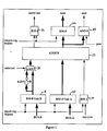
- FIG. 1 is a schematic/block diagram of a multi-bit output functional block module according to a first preferred embodiment of the present invention.
- FIG. 2 is a schematic/block diagram of a multiplexer-register element used in the construction of the multi-bit output functional block modules according to the present invention.
- FIG. 3 is a schematic/block diagram of a multi-bit output functional block module according to a second preferred embodiment of the present invention.
- FIG. 4 is a schematic/block diagram of a multi-bit output functional block module according to a third preferred embodiment of the present invention.
- the present invention is directed to a method and apparatus for providing multi-bit output functional block modules on an FPGA without using more general single-bit output FPGA modules to achieve the same functionality.
- the present invention provides functional blocks of much higher performance at much smaller cost in terms of silicon layout area consumed.
- the performance of the present invention is higher, the area cost lower and the flexibility at least comparable.
- the essence of the present invention is in designing a functional block module capable of a wide variety of often-needed multi-bit output functions and programmable using the general interconnect structure available on the FPGA.
- the functional block modules that will be described below all perform operations that are 8-bits wide. In principle any number of bits may be chosen for the width of the operation. Depending on the target usage and market for a particular FPGA, 4, 6, 12 or even 16 bits may be more appropriate. The performance improves with wider blocks, but the cost also goes up since the probability of wasting a portion of the block also increases.
- the functional blocks are not distributed to the FPGA modules.
- the size of the functional block, its shape, its circuit and the number of programmable inputs and outputs of such a functional block will be different from that of typical FPGA modules on the FPGA.
- Each functional block as a whole unit is located at a chosen location on the FPGA.
- the functional blocks have a multitude of inputs and outputs, each of which can be connected to the neighboring programmable interconnect resources.
- the communication among the functional blocks as well as between the functional blocks and the FPGA modules are done with the standard programmable interconnect resources available on the FPGA. In the case where there are more than one different type of programmable interconnection resource available, a selection can be made among them for various types. For example, the interconnection of two adders to each other to form a larger adder can (and should) have access to the fastest type of interconnect resources so as to maintain the highest (fastest) possible performance level.
- FIG. 1 a functional block module according to a first preferred embodiment of the present invention is depicted which is capable of performing any of the following 1 to 8 bit user selectable functions is depicted:
- the functional block shown in FIG. 1 is only one of many possible functional blocks. Furthermore, depending upon the intended range of applications, it may be preferable to divide the functionality of this block up into two or more separate functional blocks with programmable and high performance interconnect connecting them. For example, the functions (f), (g) and (h) can be easily separated from functions (a), (b), (c) and (d). In that case, functions (e) and (i) can still be performed by using interconnected combinations of these sub-blocks.
- the functions above are selectable by appropriately configuring various inputs of the module to either logic 0 or logic 1.
- all of the functions can be selected "on the fly” by the value at the data inputs while the circuit is in operation.
- the circuit can switch from an adder to a subtracter, or to an AND gate, depending on the data inputs.
- the function (e) involves interconnecting the outputs and the inputs of the functional block using the FPGA interconnect, and thus can not be converted to another function while the circuit is in operation.
- the blocks 10 and 12 of FIG. 1 are a combination of a register 14 and a multiplexer 16. This is shown in detail in FIG. 2.
- the register 14 is a simple D-flip-flop, but it may have additional features like CLEAR, PRESET, ENABLE and the like.
- the blocks 18, 20 and 22 respectively labelled "RM-8 UNIT B", “RM-8 UNIT A” and “RM-8” in FIG. 1 are 8-bit wide parallel arrangements of the blocks RM-1, where the DATA inputs to each RM-1 are different, but the CLOCK and the REGISTER BYPASS inputs are common to all. If there are additional inputs for CLEAR, PRESET, ENABLE, and the like, they too are made common to all 8 RM-1 blocks within the RM-8 block.
- the block 24 labelled "AND-9" in FIG. 1 is a simple 9-input AND gate.
- the block 26 labelled "8-INV" in FIG. 1 is a bank of 8 parallel inverters which simply inverts the 8-bit wide signal.
- the block 28 labelled "8-MX2" in FIG. 1 is a bank of 8 parallel 2-input multiplexers.
- the SELECT input for the multiplexers (named SUBTRACT) is common to all of them.
- ADDER is an 8-bit adder having two 8-bit inputs and a CARRY output.
- Such adders are well known to those of ordinary skill in the art.
- DATA means that the value can be any input value
- DATA ⁇ means the opposite value of the previous or the next column's DATA, whichever is applicable
- ADDR means the address value that is to be decoded
- X means that the information is irrelevant.
- FIG. 3 represents a second preferred embodiment of the present invention.
- FIG. 3 represents the FIG. 1 embodiment to which is added the circuitry shown in box 30.
- a 2-bit multiplexer 32 labelled "MX-2" is used to multiplex the CARRY OUT signal from RM-1 (12) with the OTHER-CARRY signal.
- Multiplexer 34 is an 8-bit wide parallel array of 2-bit multiplexers using OTHER-SELECT and multiplexing the SUM outputs from RM-8 (22) with OTHER-SUM.
- this additional circuitry is to permit such operations as parallel addition. For example, if it is desired to add numbers comprising more than 8 bits, say, two pairs of 8-bit numbers, by adding the lower order 8-bits in a first adder and by adding the higher order 8-bits in both a second adder and a third adder, the second adder assuming that the carry from the first adder will be zero and the third adder assuming that the carry from the first adder will be one, all three operations can be performed in parallel at the same time using the multiplexer at block 32 to select the appropriate higher order result.
- the cost is the use of additional functional blocks, but the elapsed time for the procedure is almost alved.
- FIG. 4 represents a third preferred embodiment of the present invention.
- FIG. 4 is similar to FIG. 1 except that the input registers have been omitted. Much of the functionality is retained, i.e., the FIG. 4 embodiment is capable of being programmed to perform the very same functions where the variety of register implementations are fewer, and pipelined adder/subtracter operation is not possible, yet the amount of real estate required is reduced by about 25% over the FIG. 1 embodiment for MUX-based (multiplexer-based) and anti-fuse connected FPGAs.
Abstract
Description
- This invention relates to the field of Field Programmable Gate Arrays (FPGAs). More particularly, it relates to a method and apparatus for improving the efficiency of FPGAs by inclusion of programmable dedicated multi-bit output functional blocks within FPGAs.
- FPGAs comprise a multitude of FPGA logic modules (the smallest programmable functional blocks on an FPGA) which in turn comprise a plurality of FPGA gates. FPGAs are user programmed to carry out desired functions. Examples of FPGAs are described in U.S. Patent 4,758,745 to Elgamal et al. and U.S. Patent 4,870,302 to Freeman.
- Logic modules of FPGAs generally comprise multi-bit input, single-bit output devices which are programmable to create any desired output from a given input. This is accomplished in the prior art with multiplexer structures, look-up tables and logic gates, Logic modules are generally not programmable on the fly but are usually programmed by the user in a substantially permanent way.
- While FPGAs present an excellent and extremely flexible method of dealing with the processing of various digital signals, a relatively large number of FPGA logic modules are typically required in order to fashion such typical multi-bit functional blocks as adders, subtracters, magnitude comparators, identity comparators, up/down counters, registers, and multi-bit AND gates. Typically, several of these functional blocks are used for every few thousand FPGA gates. Using current technology, this can require a great number of FPGA modules to be dedicated to providing the functionality of these predictably required functional blocks.
- There are two major drawbacks to building these functional blocks out of FPGA logic modules: first, it uses more surface area or "real estate" on the chip than is absolutely necessary; second, the performance of functional blocks built out of FPGA logic modules is much lower than the performance of even corresponding ASIC standard cells configured to do the same thing.
- Another method of providing the functionality of the aforementioned functional blocks is to provide some additional distributed capability which resides in each of (or at least in a large number of) the individual FPGA logic modules. These enhancements can then be combined with the basic capabilities of the FPGA logic module itself to construct functional blocks which deliver higher performance in a smaller area than permitted by simply configuring standard FPGA modules to perform these functions. The drawback here is that the added distributed capability is purchased at the cost of reduced flexibility and freedom available to the placement and routing programs which likely will reduce the performance of other portions of the FPGA. Examples of such approaches are found in the carry chain feature incorporated in the XC-4000 products of Xilinx, Inc. of San Jose, California and the EPM-7000 product of Altera Corporation, of San Jose, California.
- Accordingly, it is an object of the present invention to provide an improved FPGA which is capable of providing the functionality of multi-bit output functional blocks such as adders, subtracters, magnitude comparators, identity comparators, up/down counters, registers, and multi-bit AND gates in reduced area with enhanced performance.
- It is a further object of the present invention to provide an improved FPGA which provides a plurality of multi-bit output functional blocks capable of performing multi-bit output functions without requiring the use of FPGA logic modules.
- It is a further object of the present invention to provide an FPGA having improved performance.
- Yet a further object of the present invention is to provide an FPGA which requires less chip area to perform the same tasks as an FPGA not incorporating the advantages of the present invention.
- These and many other objects and advantages of the present invention will become apparent to those of ordinary skill in the art from a consideration of the drawings and ensuing description of the invention.
- According to the present invention, a plurality of programmable multi-bit output functional block modules, each capable of assuming the functionality of one of the set of adders, subtracters, magnitude comparators, identity comparators, up/down counters, registers, multi-bit AND gates, and similar devices, are placed in predetermined locations of the FPGA chip. The number of functional blocks is much fewer than the number of FPGA modules on the chip. Each of the functional blocks has a plurality of inputs and outputs, each of which is capable of being connected to the neighboring programmable interconnect resources. Communication between and amongst functional blocks is carried out with the standard programmable resources available on board the FPGA chip.
- The present invention will be further described hereinafter with reference to the following description of exemplary embodiments and the accompanying drawings, in which:-
- FIG. 1 is a schematic/block diagram of a multi-bit output functional block module according to a first preferred embodiment of the present invention.
- FIG. 2 is a schematic/block diagram of a multiplexer-register element used in the construction of the multi-bit output functional block modules according to the present invention.
- FIG. 3 is a schematic/block diagram of a multi-bit output functional block module according to a second preferred embodiment of the present invention.
- FIG. 4 is a schematic/block diagram of a multi-bit output functional block module according to a third preferred embodiment of the present invention.
- Those of ordinary skill in the art will realize that the following description of the present invention is illustrative only and is not intended to be in any way limiting. Other embodiments of the invention will readily suggest themselves to such skilled persons from an examination of the within disclosure.
- The present invention is directed to a method and apparatus for providing multi-bit output functional block modules on an FPGA without using more general single-bit output FPGA modules to achieve the same functionality.
- While not comparable in flexibility to building functional blocks out of FPGA modules, the present invention provides functional blocks of much higher performance at much smaller cost in terms of silicon layout area consumed. When compared against providing some distributed capability in each (or most) FPGA modules, the performance of the present invention is higher, the area cost lower and the flexibility at least comparable.
- The essence of the present invention is in designing a functional block module capable of a wide variety of often-needed multi-bit output functions and programmable using the general interconnect structure available on the FPGA.
- The functional block modules that will be described below all perform operations that are 8-bits wide. In principle any number of bits may be chosen for the width of the operation. Depending on the target usage and market for a particular FPGA, 4, 6, 12 or even 16 bits may be more appropriate. The performance improves with wider blocks, but the cost also goes up since the probability of wasting a portion of the block also increases.
- An 8-bit block can be used to implement one or more N-bit wide functions for all N, where N=1, 2, 3, ..., 8. If the desired function is wider than 8 bits, then several functional blocks can be combined and interconnected with the programmable interconnect structure of the FPGA to accommodate the desired size. To build a 13-bit wide adder, for example, one can simply use two blocks of 8-bit adders.
- The functional blocks are not distributed to the FPGA modules. The size of the functional block, its shape, its circuit and the number of programmable inputs and outputs of such a functional block will be different from that of typical FPGA modules on the FPGA. Each functional block as a whole unit is located at a chosen location on the FPGA. The functional blocks have a multitude of inputs and outputs, each of which can be connected to the neighboring programmable interconnect resources. The communication among the functional blocks as well as between the functional blocks and the FPGA modules are done with the standard programmable interconnect resources available on the FPGA. In the case where there are more than one different type of programmable interconnection resource available, a selection can be made among them for various types. For example, the interconnection of two adders to each other to form a larger adder can (and should) have access to the fastest type of interconnect resources so as to maintain the highest (fastest) possible performance level.
- Turning now to FIG. 1 a functional block module according to a first preferred embodiment of the present invention is depicted which is capable of performing any of the following 1 to 8 bit user selectable functions is depicted:
- (a) adder;
- (b) subtracter;
- (c) magnitude comparator;
- (d) identity comparator;
- (e) up/down counter (the counter may count up or down as selected by the user, or it may count up and down depending upon the data inputs it receives);
- (f) registers (the registers may be inverting or non-inverting and may have other desired functionality such as CLEAR, PRESET, ENABLE, etc.);
- (g) AND gate;
- (h) options (a), (b), (c) and (d) may be combined with any desired combination of input and/or output registers; and
- (i) decoder.
- The functional block shown in FIG. 1 is only one of many possible functional blocks. Furthermore, depending upon the intended range of applications, it may be preferable to divide the functionality of this block up into two or more separate functional blocks with programmable and high performance interconnect connecting them. For example, the functions (f), (g) and (h) can be easily separated from functions (a), (b), (c) and (d). In that case, functions (e) and (i) can still be performed by using interconnected combinations of these sub-blocks.
- The functions above are selectable by appropriately configuring various inputs of the module to either logic 0 or
logic 1. Importantly, all of the functions (except function (e)) can be selected "on the fly" by the value at the data inputs while the circuit is in operation. For example, the circuit can switch from an adder to a subtracter, or to an AND gate, depending on the data inputs. The function (e), however, involves interconnecting the outputs and the inputs of the functional block using the FPGA interconnect, and thus can not be converted to another function while the circuit is in operation. - As shown in FIG. 2, the
blocks 10 and 12 of FIG. 1 (labelled "RM-1" in FIG. 1) are a combination of aregister 14 and amultiplexer 16. This is shown in detail in FIG. 2. Theregister 14 is a simple D-flip-flop, but it may have additional features like CLEAR, PRESET, ENABLE and the like. - The
blocks - The
block 24 labelled "AND-9" in FIG. 1 is a simple 9-input AND gate. - The
block 26 labelled "8-INV" in FIG. 1 is a bank of 8 parallel inverters which simply inverts the 8-bit wide signal. - The
block 28 labelled "8-MX2" in FIG. 1 is a bank of 8 parallel 2-input multiplexers. The SELECT input for the multiplexers (named SUBTRACT) is common to all of them. - The block labelled "ADDER" is an 8-bit adder having two 8-bit inputs and a CARRY output. Such adders are well known to those of ordinary skill in the art.
- In order to perform the functions listed above with this functional block, the data values needed at the inputs are shown in Table 1, below:
TABLE 1 FUNCTION BUS A BUS B CARRY IN SUBTRACT INPUT REGISTER BYPASS OUTPUT REGISTER BYPASS PREV ADDER DATA DATA DATA 0 DATA DATA X SUBTRACTER DATA DATA DATA 1 DATA DATA X MAG COMP DATA DATA 0 1 DATA DATA X IDENT COMP DATA DATA 0 1 DATA X DATA UP COUNTER START 00000001 0 0 0 0 X DOWN COUNTER START 00000001 0 1 0 0 X REGISTER DATA 00000000 0 0 DATA 
X INV REGISTER 00000000 DATA 0 1 DATA 
X AND GATE DATA 00000000 0 0 DATA X DATA DECODER ADDR DATA 0 0 1 1 X - In Table 1, "DATA" means that the value can be any input value;

- When larger (more than 8 bits wide) functional blocks are built out of multiple units, several options may be exercised depending on the FPGA's intended speed and density. The simplest option is to interconnect multiple functional block units in series to get a bigger block. For example, one could build a 24 (or fewer) bit wide adder out of 3 units. This approach is the most cost effective, but it also yields the lowest performance. The performance degradation is linear with the number of units put together to build a bigger block. In order to avoid this option where desirable, the block 8-MX2 shown in FIG. 1 may be made available either as a separate (smaller) functional block, or else it could be included as part of the functional block shown in FIG. 3. FIG. 3 represents a second preferred embodiment of the present invention.
- A second preferred embodiment of the present invention is depicted at FIG. 3. FIG. 3 represents the FIG. 1 embodiment to which is added the circuitry shown in
box 30. In this case a 2-bit multiplexer 32 labelled "MX-2" is used to multiplex the CARRY OUT signal from RM-1 (12) with the OTHER-CARRY signal.Multiplexer 34 is an 8-bit wide parallel array of 2-bit multiplexers using OTHER-SELECT and multiplexing the SUM outputs from RM-8 (22) with OTHER-SUM. - The purpose of this additional circuitry is to permit such operations as parallel addition. For example, if it is desired to add numbers comprising more than 8 bits, say, two pairs of 8-bit numbers, by adding the lower order 8-bits in a first adder and by adding the higher order 8-bits in both a second adder and a third adder, the second adder assuming that the carry from the first adder will be zero and the third adder assuming that the carry from the first adder will be one, all three operations can be performed in parallel at the same time using the multiplexer at
block 32 to select the appropriate higher order result. The cost is the use of additional functional blocks, but the elapsed time for the procedure is almost alved. - FIG. 4 represents a third preferred embodiment of the present invention. FIG. 4 is similar to FIG. 1 except that the input registers have been omitted. Much of the functionality is retained, i.e., the FIG. 4 embodiment is capable of being programmed to perform the very same functions where the variety of register implementations are fewer, and pipelined adder/subtracter operation is not possible, yet the amount of real estate required is reduced by about 25% over the FIG. 1 embodiment for MUX-based (multiplexer-based) and anti-fuse connected FPGAs.
- It is, of course, possible to build an FPGA which incorporates one or more of the functional block modules from the first, second and third preferred embodiments, or any subcombination thereof.
- While illustrative embodiments and applications of this invention have been shown and described, it would be apparent to those skilled in the art that many more modifications than have been mentioned above are possible without departing from the inventive concepts set forth herein. The invention, therefore, is not to be limited except as defined in the appended claims.
Claims (7)
- A user programmable FPGA architecture disposed on an integrated circuit, said architecture comprising:
a general interconnect structure;
a plurality of FPGA logic modules, each of said FPGA logic modules including I inputs and J outputs;
a plurality of functional block modules, each of said functional block modules including K inputs and L outputs, wherein K>I and L>J. - A user programmable FPGA architecture disposed on an integrated circuit, according to claim 1, wherein said functional block modules are adapted for performing combinatorial operations on a first N-bit data word and a second N-bit data word, for N ≧ 2, provided by a corresponding first N-bit input data bus and a second N-bit input data bus, each of said functional block modules being independently programmable to perform one of the functions selected from the group of adder, counter, comparator, and AND gate.
- The user programmable FPGA architecture according to claim 2, wherein said functional block modules are programmable to perform one of the functions selected from the group of adder, counter, comparator, and AND gate based upon the states of a subset of said K inputs.
- A user programmable FPGA architecture according to claim 1, wherein said functional block modules are adapted for performing combinatorial operations on a first N-bit data word and a second N-bit data word, for N ≧ 2, provided by a corresponding first N-bit input data bus and a second N-bit input data bus, each of said functional block modules being independently programmable to perform one of the functions selected from the group of adder and AND gate.
- A user programmable FPGA architecture disposed on an integrated circuit, said architecture comprising:
a general interconnect structure;
a plurality of FPGA logic modules;
a plurality of functional block modules for performing combinatorial operations on a first N-bit data word and a second N-bit data word, for N ≧ 2, provided by a corresponding first N-bit input data bus and a second N-bit input data bus, each of said functional block modules independently programmable to perform one of the functions selected from the group of adder, subtracter, up-counter, down-counter, magnitude comparator, identity comparator, register, inverting register, AND gate, and decoder, said functional block modules including
an N-bit adder operatively connected to said first N-bit input data bus and said second N-bit input data bus, and
an N-bit adder output bus operatively connected to both an N+1 bit adder and an array of N 2-bit multiplexers. - A user programmable FPGA architecture according to claim 5, wherein said functional block modules further include:
a first array of N 2-bit multiplexers having an input connected to said first N-bit input data bus and an output connected to a first N-bit multiplexer output; and
a second array of N 2-bit multiplexers having an input connected to said second N-bit input data bus and an output connected to a second N-bit multiplexer output; wherein said N-bit adder is operatively connected to said first N-bit multiplexer output and said second N-bit multiplexer output, and
said N-bit adder output bus is operatively connected to both an N+1 bit adder and a third array of N-2-bit multiplexers. - A user programmable FPGA architecture according to claim 6, said functional block modules further include:
an N-bit inverter having an inverter input and an inverter output, said inverter input operatively connected to said second N-bit multiplexer output; and
a third array of N 2-bit multiplexers having a first input connected to said inverter output, a second input connected to said second N-bit multiplexer output, and an N-bit output; wherein
said N-bit adder is operatively connected to said first N-bit multiplexer output and said N-bit output of said third array of N 2-bit multiplexers, and
said N-bit adder output bus is operatively connected to both an N+1 bit adder and a fourth array of N 2-bit multiplexers.
Applications Claiming Priority (2)
| Application Number | Priority Date | Filing Date | Title |
|---|---|---|---|
| US144452 | 1993-10-27 | ||
| US08/144,452 US5448185A (en) | 1993-10-27 | 1993-10-27 | Programmable dedicated FPGA functional blocks for multiple wide-input functions |
Publications (2)
| Publication Number | Publication Date |
|---|---|
| EP0651514A2 true EP0651514A2 (en) | 1995-05-03 |
| EP0651514A3 EP0651514A3 (en) | 1997-03-05 |
Family
ID=22508651
Family Applications (1)
| Application Number | Title | Priority Date | Filing Date |
|---|---|---|---|
| EP94307703A Withdrawn EP0651514A3 (en) | 1993-10-27 | 1994-10-20 | Programmable dedicated FPGA functional blocks for multiple wide-input functions. |
Country Status (3)
| Country | Link |
|---|---|
| US (1) | US5448185A (en) |
| EP (1) | EP0651514A3 (en) |
| JP (1) | JPH07273638A (en) |
Cited By (7)
| Publication number | Priority date | Publication date | Assignee | Title |
|---|---|---|---|---|
| WO2002103908A1 (en) * | 2001-06-20 | 2002-12-27 | Telefonaktiebolaget Lm Ericsson (Publ) | Upgrading field programmable gate arrays overs data-communication networks |
| EP2226726A3 (en) * | 2003-12-19 | 2010-10-20 | MicroUnity Systems Engineering, Inc. | Programmable processor and method with wide operations |
| US7889204B2 (en) | 1998-08-24 | 2011-02-15 | Microunity Systems Engineering, Inc. | Processor architecture for executing wide transform slice instructions |
| US7932911B2 (en) | 1998-08-24 | 2011-04-26 | Microunity Systems Engineering, Inc. | Processor for executing switch and translate instructions requiring wide operands |
| EP1271474B1 (en) * | 2001-06-25 | 2011-11-02 | NEC Corporation | Function block |
| CN105278394A (en) * | 2014-07-18 | 2016-01-27 | 京微雅格(北京)科技有限公司 | Circuit and method of parallel configuration on the basis of FPGA (Field-Programmable Gate Array) |
| US9785565B2 (en) | 2014-06-30 | 2017-10-10 | Microunity Systems Engineering, Inc. | System and methods for expandably wide processor instructions |
Families Citing this family (11)
| Publication number | Priority date | Publication date | Assignee | Title |
|---|---|---|---|---|
| US5477165A (en) * | 1986-09-19 | 1995-12-19 | Actel Corporation | Programmable logic module and architecture for field programmable gate array device |
| US5198705A (en) | 1990-05-11 | 1993-03-30 | Actel Corporation | Logic module with configurable combinational and sequential blocks |
| US5751162A (en) * | 1995-04-06 | 1998-05-12 | Texas Instruments Incorporated | Field programmable gate array logic module configurable as combinational or sequential circuits |
| US5614840A (en) * | 1995-05-17 | 1997-03-25 | Altera Corporation | Programmable logic array integrated circuits with segmented, selectively connectable, long interconnection conductors |
| US5631576A (en) * | 1995-09-01 | 1997-05-20 | Altera Corporation | Programmable logic array integrated circuit devices with flexible carry chains |
| US5936426A (en) | 1997-02-03 | 1999-08-10 | Actel Corporation | Logic function module for field programmable array |
| US5952852A (en) * | 1997-07-02 | 1999-09-14 | Actel Corporation | Fast wide decode in an FPGA using probe circuit |
| US6034542A (en) * | 1997-10-14 | 2000-03-07 | Xilinx, Inc. | Bus structure for modularized chip with FPGA modules |
| US6844756B1 (en) * | 2000-06-23 | 2005-01-18 | Cypress Semiconductor Corp. | Configurable dedicated logic in PLDs |
| JP3887622B2 (en) * | 2003-10-17 | 2007-02-28 | 松下電器産業株式会社 | Data processing device |
| US7606347B2 (en) * | 2004-09-13 | 2009-10-20 | General Electric Company | Photon counting x-ray detector with overrange logic control |
Citations (2)
| Publication number | Priority date | Publication date | Assignee | Title |
|---|---|---|---|---|
| US4870302A (en) * | 1984-03-12 | 1989-09-26 | Xilinx, Inc. | Configurable electrical circuit having configurable logic elements and configurable interconnects |
| US5122685A (en) * | 1991-03-06 | 1992-06-16 | Quicklogic Corporation | Programmable application specific integrated circuit and logic cell therefor |
Family Cites Families (7)
| Publication number | Priority date | Publication date | Assignee | Title |
|---|---|---|---|---|
| US4763020B1 (en) * | 1985-09-06 | 1997-07-08 | Ricoh Kk | Programmable logic device having plural programmable function cells |
| US4771285A (en) * | 1985-11-05 | 1988-09-13 | Advanced Micro Devices, Inc. | Programmable logic cell with flexible clocking and flexible feedback |
| US4758745B1 (en) * | 1986-09-19 | 1994-11-15 | Actel Corp | User programmable integrated circuit interconnect architecture and test method |
| US4983959A (en) * | 1986-10-01 | 1991-01-08 | Texas Instruments Incorporated | Logic output macrocell |
| US5028821A (en) * | 1990-03-01 | 1991-07-02 | Plus Logic, Inc. | Programmable logic device with programmable inverters at input/output pads |
| US5245227A (en) * | 1990-11-02 | 1993-09-14 | Atmel Corporation | Versatile programmable logic cell for use in configurable logic arrays |
| US5220213A (en) * | 1991-03-06 | 1993-06-15 | Quicklogic Corporation | Programmable application specific integrated circuit and logic cell therefor |
-
1993
- 1993-10-27 US US08/144,452 patent/US5448185A/en not_active Expired - Lifetime
-
1994
- 1994-10-20 EP EP94307703A patent/EP0651514A3/en not_active Withdrawn
- 1994-10-27 JP JP6287346A patent/JPH07273638A/en active Pending
Patent Citations (2)
| Publication number | Priority date | Publication date | Assignee | Title |
|---|---|---|---|---|
| US4870302A (en) * | 1984-03-12 | 1989-09-26 | Xilinx, Inc. | Configurable electrical circuit having configurable logic elements and configurable interconnects |
| US5122685A (en) * | 1991-03-06 | 1992-06-16 | Quicklogic Corporation | Programmable application specific integrated circuit and logic cell therefor |
Non-Patent Citations (4)
| Title |
|---|
| ELECTRONIC ENGINEERING, vol. 64, no. 783, March 1992, WOOLWICH, LONDON, GB, pages 57-63, XP000298023 B. HAMILTON ET AL.: "Design issues from FPGA and PLD architectural differences" * |
| IEEE DESIGN & TEST OF COMPUTERS, vol. 9, no. 3, September 1992, LOS ALAMITOS, CA, US, pages 3-5, XP000306601 S. TRIMBERGER: "Field-Programmable Gate Arrays" * |
| WESCON CONFERENCE RECORD, vol. 35, November 1991, NORTH HOLLYWOOD, CA, US, pages 46-54, XP000320514 W. MILLER: "System design considerations using field programmable gate arrays" * |
| WESCON CONFERENCE RECORD, vol. 36, 17 - 19 November 1992, NORTH HOLLYWOOD, CA, US, pages 107-110, XP000350081 S.S. VIJ: "Eliminating Routing Bottlenecks in High Density Programmable Architectures" * |
Cited By (19)
| Publication number | Priority date | Publication date | Assignee | Title |
|---|---|---|---|---|
| US7932910B2 (en) | 1995-08-16 | 2011-04-26 | Microunity Systems Engineering, Inc. | System and software for performing matrix multiply extract operations |
| US8289335B2 (en) | 1995-08-16 | 2012-10-16 | Microunity Systems Engineering, Inc. | Method for performing computations using wide operands |
| US8018464B2 (en) | 1998-08-24 | 2011-09-13 | Microunity Systems Engineering, Inc. | Computer system for executing switch and table translate instructions requiring wide operands |
| US9378018B2 (en) | 1998-08-24 | 2016-06-28 | Microunity Systems Engineering, Inc. | Processor for executing wide operand operations using a control register and a results register |
| US7932911B2 (en) | 1998-08-24 | 2011-04-26 | Microunity Systems Engineering, Inc. | Processor for executing switch and translate instructions requiring wide operands |
| US7940277B2 (en) | 1998-08-24 | 2011-05-10 | Microunity Systems Engineering, Inc. | Processor for executing extract controlled by a register instruction |
| US7948496B2 (en) | 1998-08-24 | 2011-05-24 | Microunity Systems Engineering, Inc. | Processor architecture with wide operand cache |
| US7952587B2 (en) | 1998-08-24 | 2011-05-31 | Microunity Systems Engineering, Inc. | Processor and method for executing instructions requiring wide operands for multiply matrix operations |
| US10365926B2 (en) | 1998-08-24 | 2019-07-30 | Microunity Systems Engineering, Inc. | Processor and method for executing wide operand multiply matrix operations |
| US7889204B2 (en) | 1998-08-24 | 2011-02-15 | Microunity Systems Engineering, Inc. | Processor architecture for executing wide transform slice instructions |
| US8269784B2 (en) | 1998-08-24 | 2012-09-18 | Microunity Systems Engineering, Inc. | Processor architecture for executing wide transform slice instructions |
| US9229713B2 (en) | 1998-08-24 | 2016-01-05 | Microunity Systems Engineering, Inc. | Processor for executing wide operand operations using a control register and a results register |
| US8812821B2 (en) | 1998-08-24 | 2014-08-19 | Microunity Systems Engineering, Inc. | Processor for performing operations with two wide operands |
| WO2002103908A1 (en) * | 2001-06-20 | 2002-12-27 | Telefonaktiebolaget Lm Ericsson (Publ) | Upgrading field programmable gate arrays overs data-communication networks |
| EP1271474B1 (en) * | 2001-06-25 | 2011-11-02 | NEC Corporation | Function block |
| EP2226726A3 (en) * | 2003-12-19 | 2010-10-20 | MicroUnity Systems Engineering, Inc. | Programmable processor and method with wide operations |
| US9785565B2 (en) | 2014-06-30 | 2017-10-10 | Microunity Systems Engineering, Inc. | System and methods for expandably wide processor instructions |
| US10204055B2 (en) | 2014-06-30 | 2019-02-12 | Microunity Systems Engineering, Inc. | System and methods for expandably wide processor instructions |
| CN105278394A (en) * | 2014-07-18 | 2016-01-27 | 京微雅格(北京)科技有限公司 | Circuit and method of parallel configuration on the basis of FPGA (Field-Programmable Gate Array) |
Also Published As
| Publication number | Publication date |
|---|---|
| US5448185A (en) | 1995-09-05 |
| EP0651514A3 (en) | 1997-03-05 |
| JPH07273638A (en) | 1995-10-20 |
Similar Documents
| Publication | Publication Date | Title |
|---|---|---|
| EP0651514A2 (en) | Programmable dedicated FPGA functional blocks for multiple wide-input functions | |
| US5338983A (en) | Application specific exclusive of based logic module architecture for FPGAs | |
| US6066960A (en) | Programmable logic device having combinational logic at inputs to logic elements within logic array blocks | |
| US5898602A (en) | Carry chain circuit with flexible carry function for implementing arithmetic and logical functions | |
| US5633601A (en) | Field programmable gate array logic module configurable as combinational or sequential circuits | |
| US6449628B1 (en) | Apparatus and method for programmable datapath arithmetic arrays | |
| US7274211B1 (en) | Structures and methods for implementing ternary adders/subtractors in programmable logic devices | |
| US7075333B1 (en) | Programmable circuit optionally configurable as a lookup table or a wide multiplexer | |
| US6903573B1 (en) | Programmable logic device with enhanced wide input product term cascading | |
| US7062520B2 (en) | Multi-scale programmable array | |
| EP2306331B1 (en) | Integrated circuit with cascading DSP slices | |
| EP2391010B1 (en) | A programmable logic device having complex logic blocks with improved logic cell functionality | |
| US5483178A (en) | Programmable logic device with logic block outputs coupled to adjacent logic block output multiplexers | |
| US5389843A (en) | Simplified structure for programmable delays | |
| EP1397863B1 (en) | Reconfigurable logic device | |
| US9292474B1 (en) | Configurable hybrid adder circuitry | |
| US6201409B1 (en) | High performance product term based carry chain scheme | |
| US5631576A (en) | Programmable logic array integrated circuit devices with flexible carry chains | |
| KR20180053314A (en) | Cascaded lookup table (LUT) carry logic circuit | |
| US8667046B2 (en) | Generalized programmable counter arrays | |
| US8072238B1 (en) | Programmable logic device architecture with the ability to combine adjacent logic elements for the purpose of performing high order logic functions | |
| US6075380A (en) | Programmable logic device with expandable-width memory regions | |
| WO2004003778A2 (en) | Loosely-biased heterogeneous reconfigurable arrays | |
| US7268584B1 (en) | Adder circuitry for a programmable logic device | |
| US7459932B1 (en) | Programmable logic device having logic modules with improved register capabilities |
Legal Events
| Date | Code | Title | Description |
|---|---|---|---|
| PUAI | Public reference made under article 153(3) epc to a published international application that has entered the european phase |
Free format text: ORIGINAL CODE: 0009012 |
|
| AK | Designated contracting states |
Kind code of ref document: A2 Designated state(s): DE FR GB IT |
|
| PUAL | Search report despatched |
Free format text: ORIGINAL CODE: 0009013 |
|
| AK | Designated contracting states |
Kind code of ref document: A3 Designated state(s): DE FR GB IT |
|
| 17P | Request for examination filed |
Effective date: 19970429 |
|
| 17Q | First examination report despatched |
Effective date: 19990802 |
|
| STAA | Information on the status of an ep patent application or granted ep patent |
Free format text: STATUS: THE APPLICATION IS DEEMED TO BE WITHDRAWN |
|
| 18D | Application deemed to be withdrawn |
Effective date: 20000215 |