EP0651577A2 - Digital television system - Google Patents
Digital television system Download PDFInfo
- Publication number
- EP0651577A2 EP0651577A2 EP94116984A EP94116984A EP0651577A2 EP 0651577 A2 EP0651577 A2 EP 0651577A2 EP 94116984 A EP94116984 A EP 94116984A EP 94116984 A EP94116984 A EP 94116984A EP 0651577 A2 EP0651577 A2 EP 0651577A2
- Authority
- EP
- European Patent Office
- Prior art keywords
- video signals
- operable
- input video
- video signal
- video
- Prior art date
- Legal status (The legal status is an assumption and is not a legal conclusion. Google has not performed a legal analysis and makes no representation as to the accuracy of the status listed.)
- Granted
Links
Images


Classifications
-
- H—ELECTRICITY
- H04—ELECTRIC COMMUNICATION TECHNIQUE
- H04N—PICTORIAL COMMUNICATION, e.g. TELEVISION
- H04N9/00—Details of colour television systems
- H04N9/64—Circuits for processing colour signals
- H04N9/68—Circuits for processing colour signals for controlling the amplitude of colour signals, e.g. automatic chroma control circuits
- H04N9/69—Circuits for processing colour signals for controlling the amplitude of colour signals, e.g. automatic chroma control circuits for modifying the colour signals by gamma correction
-
- H—ELECTRICITY
- H04—ELECTRIC COMMUNICATION TECHNIQUE
- H04N—PICTORIAL COMMUNICATION, e.g. TELEVISION
- H04N21/00—Selective content distribution, e.g. interactive television or video on demand [VOD]
- H04N21/40—Client devices specifically adapted for the reception of or interaction with content, e.g. set-top-box [STB]; Operations thereof
- H04N21/43—Processing of content or additional data, e.g. demultiplexing additional data from a digital video stream; Elementary client operations, e.g. monitoring of home network or synchronising decoder's clock; Client middleware
- H04N21/434—Disassembling of a multiplex stream, e.g. demultiplexing audio and video streams, extraction of additional data from a video stream; Remultiplexing of multiplex streams; Extraction or processing of SI; Disassembling of packetised elementary stream
-
- H—ELECTRICITY
- H04—ELECTRIC COMMUNICATION TECHNIQUE
- H04N—PICTORIAL COMMUNICATION, e.g. TELEVISION
- H04N19/00—Methods or arrangements for coding, decoding, compressing or decompressing digital video signals
- H04N19/42—Methods or arrangements for coding, decoding, compressing or decompressing digital video signals characterised by implementation details or hardware specially adapted for video compression or decompression, e.g. dedicated software implementation
- H04N19/423—Methods or arrangements for coding, decoding, compressing or decompressing digital video signals characterised by implementation details or hardware specially adapted for video compression or decompression, e.g. dedicated software implementation characterised by memory arrangements
-
- H—ELECTRICITY
- H04—ELECTRIC COMMUNICATION TECHNIQUE
- H04N—PICTORIAL COMMUNICATION, e.g. TELEVISION
- H04N19/00—Methods or arrangements for coding, decoding, compressing or decompressing digital video signals
- H04N19/42—Methods or arrangements for coding, decoding, compressing or decompressing digital video signals characterised by implementation details or hardware specially adapted for video compression or decompression, e.g. dedicated software implementation
- H04N19/436—Methods or arrangements for coding, decoding, compressing or decompressing digital video signals characterised by implementation details or hardware specially adapted for video compression or decompression, e.g. dedicated software implementation using parallelised computational arrangements
-
- H—ELECTRICITY
- H04—ELECTRIC COMMUNICATION TECHNIQUE
- H04N—PICTORIAL COMMUNICATION, e.g. TELEVISION
- H04N19/00—Methods or arrangements for coding, decoding, compressing or decompressing digital video signals
- H04N19/60—Methods or arrangements for coding, decoding, compressing or decompressing digital video signals using transform coding
- H04N19/61—Methods or arrangements for coding, decoding, compressing or decompressing digital video signals using transform coding in combination with predictive coding
-
- H—ELECTRICITY
- H04—ELECTRIC COMMUNICATION TECHNIQUE
- H04N—PICTORIAL COMMUNICATION, e.g. TELEVISION
- H04N21/00—Selective content distribution, e.g. interactive television or video on demand [VOD]
- H04N21/40—Client devices specifically adapted for the reception of or interaction with content, e.g. set-top-box [STB]; Operations thereof
- H04N21/41—Structure of client; Structure of client peripherals
- H04N21/426—Internal components of the client ; Characteristics thereof
-
- H—ELECTRICITY
- H04—ELECTRIC COMMUNICATION TECHNIQUE
- H04N—PICTORIAL COMMUNICATION, e.g. TELEVISION
- H04N21/00—Selective content distribution, e.g. interactive television or video on demand [VOD]
- H04N21/40—Client devices specifically adapted for the reception of or interaction with content, e.g. set-top-box [STB]; Operations thereof
- H04N21/43—Processing of content or additional data, e.g. demultiplexing additional data from a digital video stream; Elementary client operations, e.g. monitoring of home network or synchronising decoder's clock; Client middleware
- H04N21/44—Processing of video elementary streams, e.g. splicing a video clip retrieved from local storage with an incoming video stream, rendering scenes according to MPEG-4 scene graphs
- H04N21/4402—Processing of video elementary streams, e.g. splicing a video clip retrieved from local storage with an incoming video stream, rendering scenes according to MPEG-4 scene graphs involving reformatting operations of video signals for household redistribution, storage or real-time display
-
- H—ELECTRICITY
- H04—ELECTRIC COMMUNICATION TECHNIQUE
- H04N—PICTORIAL COMMUNICATION, e.g. TELEVISION
- H04N3/00—Scanning details of television systems; Combination thereof with generation of supply voltages
- H04N3/02—Scanning details of television systems; Combination thereof with generation of supply voltages by optical-mechanical means only
- H04N3/08—Scanning details of television systems; Combination thereof with generation of supply voltages by optical-mechanical means only having a moving reflector
-
- H—ELECTRICITY
- H04—ELECTRIC COMMUNICATION TECHNIQUE
- H04N—PICTORIAL COMMUNICATION, e.g. TELEVISION
- H04N5/00—Details of television systems
- H04N5/14—Picture signal circuitry for video frequency region
-
- H—ELECTRICITY
- H04—ELECTRIC COMMUNICATION TECHNIQUE
- H04N—PICTORIAL COMMUNICATION, e.g. TELEVISION
- H04N5/00—Details of television systems
- H04N5/14—Picture signal circuitry for video frequency region
- H04N5/144—Movement detection
-
- H—ELECTRICITY
- H04—ELECTRIC COMMUNICATION TECHNIQUE
- H04N—PICTORIAL COMMUNICATION, e.g. TELEVISION
- H04N5/00—Details of television systems
- H04N5/44—Receiver circuitry for the reception of television signals according to analogue transmission standards
-
- H—ELECTRICITY
- H04—ELECTRIC COMMUNICATION TECHNIQUE
- H04N—PICTORIAL COMMUNICATION, e.g. TELEVISION
- H04N5/00—Details of television systems
- H04N5/74—Projection arrangements for image reproduction, e.g. using eidophor
- H04N5/7416—Projection arrangements for image reproduction, e.g. using eidophor involving the use of a spatial light modulator, e.g. a light valve, controlled by a video signal
- H04N5/7458—Projection arrangements for image reproduction, e.g. using eidophor involving the use of a spatial light modulator, e.g. a light valve, controlled by a video signal the modulator being an array of deformable mirrors, e.g. digital micromirror device [DMD]
-
- H—ELECTRICITY
- H04—ELECTRIC COMMUNICATION TECHNIQUE
- H04N—PICTORIAL COMMUNICATION, e.g. TELEVISION
- H04N7/00—Television systems
- H04N7/01—Conversion of standards, e.g. involving analogue television standards or digital television standards processed at pixel level
- H04N7/0117—Conversion of standards, e.g. involving analogue television standards or digital television standards processed at pixel level involving conversion of the spatial resolution of the incoming video signal
- H04N7/012—Conversion between an interlaced and a progressive signal
-
- H—ELECTRICITY
- H04—ELECTRIC COMMUNICATION TECHNIQUE
- H04N—PICTORIAL COMMUNICATION, e.g. TELEVISION
- H04N7/00—Television systems
- H04N7/01—Conversion of standards, e.g. involving analogue television standards or digital television standards processed at pixel level
- H04N7/0135—Conversion of standards, e.g. involving analogue television standards or digital television standards processed at pixel level involving interpolation processes
-
- H—ELECTRICITY
- H04—ELECTRIC COMMUNICATION TECHNIQUE
- H04N—PICTORIAL COMMUNICATION, e.g. TELEVISION
- H04N9/00—Details of colour television systems
- H04N9/12—Picture reproducers
- H04N9/31—Projection devices for colour picture display, e.g. using electronic spatial light modulators [ESLM]
- H04N9/3141—Constructional details thereof
- H04N9/3147—Multi-projection systems
-
- H—ELECTRICITY
- H04—ELECTRIC COMMUNICATION TECHNIQUE
- H04N—PICTORIAL COMMUNICATION, e.g. TELEVISION
- H04N9/00—Details of colour television systems
- H04N9/64—Circuits for processing colour signals
- H04N9/642—Multi-standard receivers
-
- H—ELECTRICITY
- H04—ELECTRIC COMMUNICATION TECHNIQUE
- H04N—PICTORIAL COMMUNICATION, e.g. TELEVISION
- H04N9/00—Details of colour television systems
- H04N9/64—Circuits for processing colour signals
- H04N9/643—Hue control means, e.g. flesh tone control
-
- H—ELECTRICITY
- H04—ELECTRIC COMMUNICATION TECHNIQUE
- H04N—PICTORIAL COMMUNICATION, e.g. TELEVISION
- H04N9/00—Details of colour television systems
- H04N9/64—Circuits for processing colour signals
- H04N9/67—Circuits for processing colour signals for matrixing
-
- H—ELECTRICITY
- H04—ELECTRIC COMMUNICATION TECHNIQUE
- H04N—PICTORIAL COMMUNICATION, e.g. TELEVISION
- H04N9/00—Details of colour television systems
- H04N9/64—Circuits for processing colour signals
- H04N9/68—Circuits for processing colour signals for controlling the amplitude of colour signals, e.g. automatic chroma control circuits
-
- H—ELECTRICITY
- H04—ELECTRIC COMMUNICATION TECHNIQUE
- H04N—PICTORIAL COMMUNICATION, e.g. TELEVISION
- H04N19/00—Methods or arrangements for coding, decoding, compressing or decompressing digital video signals
- H04N19/30—Methods or arrangements for coding, decoding, compressing or decompressing digital video signals using hierarchical techniques, e.g. scalability
-
- H—ELECTRICITY
- H04—ELECTRIC COMMUNICATION TECHNIQUE
- H04N—PICTORIAL COMMUNICATION, e.g. TELEVISION
- H04N5/00—Details of television systems
- H04N5/74—Projection arrangements for image reproduction, e.g. using eidophor
- H04N5/7416—Projection arrangements for image reproduction, e.g. using eidophor involving the use of a spatial light modulator, e.g. a light valve, controlled by a video signal
- H04N5/7458—Projection arrangements for image reproduction, e.g. using eidophor involving the use of a spatial light modulator, e.g. a light valve, controlled by a video signal the modulator being an array of deformable mirrors, e.g. digital micromirror device [DMD]
- H04N2005/7466—Control circuits therefor
-
- H—ELECTRICITY
- H04—ELECTRIC COMMUNICATION TECHNIQUE
- H04N—PICTORIAL COMMUNICATION, e.g. TELEVISION
- H04N7/00—Television systems
- H04N7/01—Conversion of standards, e.g. involving analogue television standards or digital television standards processed at pixel level
- H04N7/0117—Conversion of standards, e.g. involving analogue television standards or digital television standards processed at pixel level involving conversion of the spatial resolution of the incoming video signal
- H04N7/0122—Conversion of standards, e.g. involving analogue television standards or digital television standards processed at pixel level involving conversion of the spatial resolution of the incoming video signal the input and the output signals having different aspect ratios
Definitions
- This invention relates in general to the field of electronic devices. More particularly, this invention relates to a digital television system.
- Standard television has not kept up with the modern electronic revolution as exemplified by the recent developments in the personal computer industry. Consequently, a standard television system does not produce as high a quality picture as one might expect given the recent advancements seen in other modern electronic systems.
- Standard television systems may receive and display analog, rather than digital, video signals.
- a typical standard video signal is referred to as an "interlaced" video signal.
- the first field may, for example, contain the odd lines of the video frame.
- the second field may contain the even lines of the same video frame.
- the two fields making up the single frame are received and displayed successively on the standard system and may appear to a viewer as a single frame. Dividing and displaying a video frame in this manner may decrease the quality of the output of a video system.
- a standard television system may include an analog display such as a cathode ray tube (hereinafter "CRT").
- CRT cathode ray tube
- a "gamma curve” is introduced into a standard video signal to compensate for the non-linearity of the CRT.
- Standard video signals therefore are not directly compatible with a linear digital display.
- a standard television system may not be operable to process a video signal prior to displaying the video signal.
- a standard television system may not be programmable to operate on a number of different standard video signals.
- a standard television system may be limited to a small display area on the order of 640 by 480 pixels.
- a digital television system which substantially eliminates or reduces disadvantages and problems associated with prior systems.
- the teachings of the present invention provide a digital television system that processes video signals in a parallel architecture.
- a parallel architecture has not been previously used in a television system.
- the present invention provides a digital television system that may process input video signals in various forms.
- the system comprises circuitry that is operable to divide a line of input video signals into a plurality of channels for each input video signal.
- the channels of input video signals are processed in parallel.
- the processed video signals may be displayed on a display.
- the channels of the system may correspond to vertical strips of a video frame.
- Each channel may contain an overlap of, for example, one to five pixels with an adjacent channel.
- the overlap between channels may allow identical horizontal processing of pixels on the ends of each channel.
- the overlapping pixels may be removed before the processed video signal is displayed such that redundant pixels are not displayed.
- the system may convert each field of an interlaced video signal into a non-interlaced frame. Additionally, the system may remove the effect of a standard gamma curve from a standard video signal.
- the display may provide 2 X intensity levels in response to X bit planes formed for each of the video signals from video data for each pixel in a video frame.
- the first bit plane for each input video signal, corresponding to the most significant bit for each pixel, may control the display for one-half of the time for one frame.
- Successive bit planes may each control the display for a period of time proportionate to the position of the bits of that bit plane in the pixels making up that bit plane.
- the system may be programmed by a user to process a particular standard video signal. Additionally, the system may be programmed to implement various functions to produce a high definition display from a standard video signal input.
- the system may expand the pixel width of a video frame by controlling the rate at which a line of video data is sampled. Additionally, the system may scale the number of lines in a video frame.
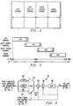
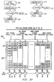
- FIGURE 1 illustrates a digital television system indicated generally at 10 and constructed according to the teachings of the present invention.
- System 10 comprises a parallel architecture wherein input video signals may be divided into channels to be processed in parallel.
- system 10 may implement appropriate functions such that a standard video signal may be used to provide a high definition video display.
- system 10 may sample and display a high definition video signal.
- System 10 may receive video signals in composite or component form.
- system 10 may receive an analog composite video signal, an analog video signal in component form, or a digital video signal.
- System 10 may convert a composite video signal into a plurality of video signals for processing.
- an analog composite video signal in the format established by the National Television Standards Committee (hereinafter "NTSC") may be separated into a luminance signal, identified by the symbol Y, and two color difference signals, identified by the symbols I and Q.
- system 10 may separate other standard composite video signals into appropriate video signals for processing according to Table 1 below.
- Each of these standard video signals comprise a luminance signal, hereinafter “luma” or “Y”, and a chrominance signal, hereinafter “chroma” or “C”.
- the chroma signal may be further divided into appropriate color difference signals as shown in Table 1.
- each of the standard video signals may hereinafter be referred to as providing a video signal in a "color difference color space” or a "Y-I-Q color space.”
- a video source may be coupled to system 10 to provide a red video signal, hereinafter “R”, a green video signal, hereinafter “G”, and a blue video signal, hereinafter "B”.
- RGB red video signal
- G green video signal
- B blue video signal
- Such a video source may hereinafter be referred to as providing a video signal in an "R-G-B color space.”
- Receiving circuitry 12 may receive, for example, a composite video signal in the NTSC format from an external source (not explicitly shown). Alternatively, receiving circuitry 12 may receive separate Y and C video signals. Furthermore, receiving circuitry 12 may receive separate video signals in an R-G-B color space.
- Receiving circuitry 12 comprises composite video interface and separation circuit 16 coupled to analog to digital converter circuit 18.
- Composite video interface and separation circuit 16 may separate a composite video signal into, for example, three separate video signals.
- Analog to digital converter circuit 18 may convert each of the separate video signals into ten bit digital video signals.
- Analog to digital converter circuit 18 of receiving circuitry 12 is coupled to provide three ten bit digital video signals to line slicer 14. Additionally, a digital video signal may be coupled directly to line slicer 14.
- Line slicer 14 divides each digital video signal into a plurality of separate channels for each line of composite video signal. For example, line slicer 14 may divide each digital video signal into four, five or another appropriate number of channels. The number of channels may depend on the number of pixels in a line of video signal, and the number of pixels that may be simultaneously processed by a video signal processor of system 10. Line slicer 14 may provide appropriate overlap between the various channels for processing as described below.
- System 10 processes the digital video signals in processing circuitry 20.
- Processing circuitry 20 is coupled to line slicer 14.
- Processing circuitry 20 comprises a plurality of channel signal processors 22a through 22d.
- the number of channel signal processors 22 may be equal to the number of channels provided by line slicer 14.
- Each channel signal processor 22a through 22d receives all three 10 bit digital video signals for the channel corresponding to that signal processor 22a through 22d.
- Processing circuitry 20 may convert each line of digital video signal into two lines of digital video signal output.
- Each channel signal processor 22a through 22d therefore, may have six separate outputs, for example, two ten bit red outputs, two ten bit green outputs, and two ten bit blue outputs. Additionally, processing circuitry 20 may perform the following functions: color space conversion, gamma correction, and picture quality control which will be described in detail below.
- System 10 reconnects and displays the processed video data.
- a plurality of formatters 24a through 24c reconnect the video data and a plurality of displays 26a through 26c display the video data.
- One formatter 24a through 24c and one display 26a through 26c operate on a different digital video signal as indicated in FIGURE 1.
- formatter 24a and display 26a may operate on a red video signal.
- Formatter 28b and display 26b may operate on a green video signal.
- formatter 24c and display 26c may operate on a blue video signal.
- Displays 26a through 26c may comprise, for example, a Spatial Light Modulator (hereinafter "SLM”) such as a 2 x 128 pin Digital Micromirror Device (hereinafter "DMD”) produced by TEXAS INSTRUMENTS INCORPORATED.
- SLM Spatial Light Modulator
- DMD Digital Micromirror Device
- displays 26a through 26c are not limited to digital displays. It is within the scope of the teachings of the present invention for the processed video signal to be displayed on an analog display.
- Timing and control circuit 28 is coupled to composite video interface and separation circuit 16, analog to digital converter circuit 18, line slicer 14, processing circuitry 20, formatters 24a through 24c, and displays 26a through 26c. Timing and control circuit 28 is operable to control the timing of each aspect of system 10. The timing of system 10 may be accomplished through use of a synchronization (hereinafter "sync") signal supplied to timing and control circuit 28 by composite video interface and separation circuit 16. Additionally, timing and control circuit 28 is operable to accept user inputs to control the timing of various functions of system 10. For example, timing and control circuit 28 may receive user inputs to select the type of input video signal coupled to receiving circuitry 12.
- timing and control circuit 28 may accept information for processing circuitry 20 such as a scaling factor, a gamma correction factor, the desired processing method, and picture control functions; each of which are described more fully below. Furthermore, timing and control circuit 28 may receive a specific sampling rate for analog to digital converter circuit 18.
- system 10 may prepare a standard video signal to produce a high definition display.
- system 10 may receive analog or digital video signals in composite or separated form.
- System 10 separates a composite video signal into video signals, divides the video signals into a plurality of channels, and processes the channels in parallel.
- An advantage of using a parallel architecture in system 10 is that system 10 is able to process the video signals at a low speed while providing a high definition display. Consequently, system 10 may incorporate existing video processor components.
- Composite video interface and separation circuit 16 separates the composite video signal into, for example, three separate video signals.
- Composite video interface and separation circuit 16 may, for example, separate a composite video signal into Y, I, and Q video signals of the NTSC standard.
- Analog to digital converter circuit 18 may sample each video signal at a frequency of, for example, 71.1 MHz.
- the appropriate sampling rate may depend on the number of pixels allocated for a line of video on displays 26a through 26c, and the time for one line of video signal to be received by receiving circuitry 12. Therefore, the sampling rate may be adjusted to create a predetermined number of pixels for each line of video signal.
- Analog to digital converter circuit 18 may comprise, for example, Analog to Digital Converter board AD9060 produced by ANALOG DEVICES.
- analog to digital converter circuit 18 may comprise another appropriate analog to digital converter device operable to sample data at an appropriate sampling rate on the order of 75 MHz.
- Line slicer 14 divides each digital video signal into a plurality of separate channels for each line of video signal. For example, line slicer 14 may divide each line of the digital video signal into four channels so that the video signal may be processed in parallel. By dividing each line of digital video signal in the same manner, each channel signal processor 22a through 22d effectively processes one vertical strip of each video frame.
- FIGURE 2 shows the four vertical strips processed by channel signal processors 22a through 22d for the embodiment of FIGURE 1.
- line slicer 14 may divide a line on a pixel by pixel basis or line slicer 14 may divide a video frame into horizontal strips.
- line slicer 14 may provide for overlap between the vertical channels by providing common pixels to adjacent channels as shown in FIGURE 3.
- the overlap may comprise, for example, from one to five pixels.
- the overlapping pixels may be used to provide appropriate data for each channel to perform the various functions described below as called for by processing circuitry 20.
- the amount of overlap between channels may be varied depending of the specific functions implemented in processing circuitry 20.
- Processing circuitry 20 may perform the progressive scan function (hereinafter "proscan”). Proscan "de-interlaces" a video signal by creating an entire video frame from a single or multiple video fields at the field rate. As described previously, a standard video signal may comprise two fields of video data for each frame. Additionally, processing circuitry 20 may convert the digital video signals into a different color space. For example, processing circuitry 20 may convert digital video signals from a color difference color space to an R-G-B color space. Furthermore, processing circuitry may remove a gamma curve from a standard video signal. Finally, processing circuitry 20 may control the quality of a video display in response to user inputs such as inputs for adjustments to brightness, hue, contrast, sharpness and saturation. Each of these functions is described in detail below.
- System 10 reconnects and displays the processed digital video signal using formatters 24a through 24c and displays 26a through 26c.
- Formatters 24a through 24c remove overlap between adjacent channels. Additionally, formatters 24a through 24c prepare the reconnected digital video signals for display on displays 26a through 26c.
- formatters 24a through 24c may produce a plurality of bit planes from the reconnected digital video signals. Each bit plane may correspond to a particular bit for each pixel in a particular video frame. In the embodiment of FIGURE 1, formatters 24a through 24c each may produce 10 bit planes of video data for each separate video signal that are to be provided to displays 26a through 26c in 128 bit words.
- displays 26a through 26c may project appropriate images corresponding to the processed video signals on, for example, a screen (not shown).
- the combination of the different video signals output by displays 24a through 24c result in a single, appropriately colored, image.
- system 10 may be operable to be programmed to accept any appropriate standard analog or digital video signal. Alternatively, system 10 may be preprogrammed to accept only a limited number of appropriate standard analog or digital video signals.
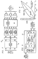
- FIGURE 4 illustrates one embodiment of a composite video interface and separation circuit indicated generally at 16 ⁇ and constructed according to the teachings of the present invention.
- Composite video interface and separation circuit 16 ⁇ may comprise, for example, Y/C separation circuit 30, luma signal multiplexer 32, chroma signal multiplexer 34, luma processing circuit 36, chroma processing circuit 38, sync signal multiplexer 40, sync separation circuit 42, and first and second output multiplexers 44 and 46.
- a composite video signal may be coupled to composite interface and separation circuit 16 ⁇ at Y/C separation circuit 30.
- Y/C separation circuit 30 separates a standard composite video signal into a luma signal, Y, and a chroma signal, C.
- a Y output of Y/C separation circuit 30 is coupled to luma signal multiplexer 32. Additionally, a separated luma signal is also coupled to luma signal multiplexer 32.
- a C output of Y/C separation circuit 30 is coupled to chroma signal multiplexer 34. Additionally, a chroma signal is coupled to chroma signal multiplexer 34.
- Luma signal multiplexer 32 is coupled to luma processing circuit 36 and sync signal multiplexer 40. Additionally, the output of chroma signal multiplexer 34 is coupled to chroma processing circuit 38.
- a refined luma signal is provided to first output multiplexer 44 by luma processing circuit 36. Additionally, a green video signal, G, is also coupled to first output multiplexer 44. The green video signal is also provided to sync signal multiplexer 40.
- Chroma processing circuit 38 provides two color difference signals to second output multiplexer 46.
- a red video signal, R, and a blue video signal, B, are provided to second output multiplexer 46.
- signal multiplexer 40 is coupled to sync separation circuit 42.
- the output of each of luma signal multiplexer 32, chroma signal multiplexer 34, signal multiplexer 40, and first and second output multiplexers 44 and 46 are controlled by a signal from timing and control circuit 28 of FIGURE 1.
- a standard video signal such as the standard video signals shown below in Table 2, may be prepared for processing by system 10 of FIGURE 1 in composite video interface and separation circuit 16 ⁇ .
- TABLE 2 Input Video Type Input Format (Interlaced) SMPTE 240 M 1840 X 517 NTSC 640 X 241.5 Wide NTSC # 853 853 X 241.5 NTSC 4.43 640 X 241.5 PAL 768 X 288.5 SECAM 768 X 288.5 Wide PAL # 1024 X 288.5
- a composite video signal is separated into Y and C video signals by Y/C separation circuit 30.
- the separated Y and C video signals may be passed to luma processing circuit 36 and chroma processing circuit 38 respectively by luma signal multiplexer 32 and chroma signal multiplexer 34.
- Luma processing circuit 36 refines the Y video signal input and provides it to first output multiplexer 44.
- First output multiplexer 44 may provide the processed Y video signal to analog to digital converter circuit 18 of FIGURE 1.
- chroma processing circuit 38 converts the C video signal into two appropriate color difference signals, such as I and Q.
- the output color difference signals are provided to second output multiplexer 46.
- Second output multiplexer 46 may provide the color difference signals to analog to digital converter circuit 18 of FIGURE 1.
- composite video interface and separation circuit 16 ⁇ may provide previously separated Y and C video signals to analog to digital converter circuit 18 of FIGURE 1.
- a previously separated Y video signal may be provided to analog to digital converter circuit 18 of FIGURE 1 by luma signal multiplexer 32, luma processing circuit 36, and first output multiplexer 44.
- a previously separated C video signal may be provided to analog to digital converter circuit 18 of FIGURE 1 by chroma signal multiplexer 34, chroma processing circuit 38 and second output multiplexer 46.
- composite video interface and separation circuit 16 ⁇ may provide component R, G and B signals to analog to digital converter circuit 18 of FIGURE 1.
- a G video signal is provided directly to first output multiplexer 44.
- R and B video signals are provided directly to second output multiplexer 46.
- first and second output multiplexers 44 and 46 provide R, G and B video signals to analog to digital converter circuit 18 of FIGURE 1.
- Composite video interface and separation circuit 16 ⁇ may also remove a sync signal from an input video signal.
- sync signal multiplexer 40 may provide either a Y video signal or a G video signal to sync separation circuit 42.
- Sync separation circuit 42 may remove a horizontal sync signal and a vertical sync signal from the video signal.
- Sync separation circuit 42 may provide the output sync signals to timing and control circuit 28 of FIGURE 1. Timing and control circuit 28 may base the timing of each operation performed in system 10 on the sync signal removed from the video signal.
- FIGURE 5 illustrates an embodiment of an analog to digital converter circuit indicated generally at 18 ⁇ and constructed according to the teachings of the present invention.
- FIGURE 5 only illustrates one analog to digital converter of analog to digital converter circuit 18 ⁇ .
- analog to digital converter circuit 18 of FIGURE 1 may comprise one analog to digital converter circuit 18 ⁇ illustrated in FIGURE 5 for each separate video signal to be processed by system 10 of FIGURE 1.
- analog to digital converter circuit 18 ⁇ will be described herein only in conjunction with the circuitry shown in FIGURE 5 for converting one video signal from an analog signal to a digital signal.
- Analog to digital converter circuit 18 ⁇ comprises line 47, first low pass filter 48, second low pass filter 50, multiplexer 52, multiplier 54, adder 56, and A/D converter 58.
- a separated video signal from composite video interface and separation circuit 16 of FIGURE 1 is coupled to first low pass filter 48, second low pass filter 50, and multiplexer 52.
- the output of first low pass filter 48 and second low pass filter 50 are also coupled to multiplexer 52.
- the output of multiplexer 52 is controlled by a signal from timing and control circuit 28.
- Multiplexer 52 is coupled to multiplier 54.
- Multiplier 54 amplifies the output of multiplexer 52 according to a control signal, GAIN ADJ, from timing and control circuit 28.
- Multiplier 54 is coupled to adder 56.
- Adder 56 is coupled to A/D converter 58.
- Adder 56 is also controlled by a signal from timing and control circuit 28. Additionally, an output of A/D converter 58 is coupled to adder 56.
- a video signal is provided to analog to digital converter circuit 18 ⁇ .
- the video signal may be filtered in first low pass filter 48 or second low pass filter 50 to prevent aliasing in A/D converter 58.
- first low pass filter 48 may comprise a low pass filter having a roll-off point at 30 MHz or other appropriate frequency for filtering a Y video signal.
- second low pass filter 58 may comprise a low pass filter having a roll-off point at 15 MHz or other appropriate frequency for filtering a color difference signal.
- a video signal may be provided directly to multiplexer 52 without filtering via line 47.
- the magnitude of the video signal may be adjusted in multiplier 54 to scale a voltage of, for example, 0.5 Volts peak-to-peak to the maximum analog input level of A/D converter 58. Additionally, a DC offset may be added in adder 56 to adjust the DC value of the component video signal to a predetermined level. Finally, the component video signal is sampled at an appropriate sampling rate, such as 71.1 MHz in A/D converter 58. The output of A/D converter 58 is provided to line slicer 14 of FIGURE 1.
- FIGURE 6 illustrates an embodiment of a line slicer indicated generally at 14 ⁇ and constructed according to the teachings of the present invention.
- the purpose of line slicer 14 ⁇ is to divide each digital video signal into a plurality of separate channels for each line of composite video signal such that system 10 may process the separate channels in parallel.
- Line slicer 14 ⁇ comprises multiplexer 59, slow down logic circuit 60, and a plurality of first in-first out buffer memories 62.
- Multiplexer 59 receives input for line slicer 14 ⁇ .
- Multiplexer 59 is coupled to analog to digital converter 18 of FIGURE 1.
- Analog to digital converter 18 may provide digital video signals in a Y-I-Q color space or an R-G-B color space.
- multiplexer 59 is coupled to receive digital video signals in either the Y-I-Q or R-G-B color space.
- multiplexer 59 may be coupled to receive digital video signals in the SMPTE 260M format.
- Multiplexer 59 is coupled to slow down logic 60. The output of multiplexer 59 is controlled by a signal from timing and control circuit 28.
- Slow down logic 60 compensates for a difference in speed between analog to digital converter 18 and first in-first out buffer memories 62 as described below.
- Multiplexer 59 provides three separate video signals to slow down logic circuit 60.
- analog to digital converter circuit 18 may provide Y, I, and Q video signals to slow down logic circuit 60.
- Slow down logic circuit 60 may include two outputs for each video signal input. Both Y video outputs of slow down logic circuit 60 may be coupled to one first in-first out buffer memory 62 for each channel of processing circuitry 20. Additionally, each I video signal output of slow down logic circuit 60 may be coupled to a first in-first out buffer memory 62 for each channel of processing circuitry 20. Finally, each Q video signal output of slow down logic circuit 60 may be coupled to a first in-first out buffer memory 62 for each channel of channel signal processor 20.
- line slicer 14 ⁇ may divide each line of video data processed by analog to digital converter circuit 18 of FIGURE 1 into separate channels. As shown for this embodiment, line slicer 14 ⁇ divides each line of video data into four channels. As described previously, line slicer 14 ⁇ may divide each line of video data into five channels or another appropriate number of channels.
- Slow down logic circuit 60 may be used to compensate for a difference in operating speed between analog to digital converter circuit 18 and first in-first out buffer memories 62.
- analog to digital converter circuit 18 of FIGURE 1 may comprise ECL circuitry
- first in-first out buffer memory 62 may comprise TTL circuitry.
- ECL circuitry may operate at a higher speed than TTL circuitry
- slow down logic circuit 60 may output data at, for example, one-half of the rate at which slow down logic circuit 60 receives data from analog to digital converter circuit 18 via multiplexer 59.
- slow down logic circuit 60 may receive video signals wherein each pixel comprises a 10 bit word.
- Slow down logic circuit 60 may output the same video signal in 20 bit words by combining 10 bit words for successive pixels and outputting the combined words simultaneously.
- Timing and control circuit 28 of FIGURE 1 controls the location in which each pixel of video signal is stored within first in-first out buffer memories 62.
- the output of first in-first out buffer memory 62 is provided to processing circuitry 20 of FIGURE 1.
- FIGURE 7 illustrates an embodiment of a channel signal processor indicated generally at 22 ⁇ and constructed according to the teachings of the present invention.
- Processing circuitry 20 of FIGURE 1 may comprise one channel signal processor 22 ⁇ of FIGURE 7 for each channel provided in system 10 of FIGURE 1.
- the invention is not intended to be so limited.
- Channel signal processor 22 ⁇ comprises first and second matrix multiplication circuits 64 and 66, first and second look up tables 68 and 70 and a plurality of processing modules 72a through 72c.
- First matrix multiplication circuit 64 may be coupled to receive three digital video signals from line slicer 14 corresponding to one processing channel of system 10.
- First look up table 68 is coupled to three outputs of first matrix multiplication circuit 64.
- Each processing module 72a through 72c is coupled to one output of first look up table 68 to process one digital video signal.
- Each processing module 72a through 72c provides two outputs.
- Second matrix multiplication circuit 66 is coupled to each output of processing modules 72a through 72c.
- Second look up table 70 is coupled to each output of second matrix multiplication circuit 66.
- Second look up table 70 provides six outputs, e.g. two red outputs, two green outputs, and two blue outputs to formatter 24a through 24c of FIGURE 1.
- the functions performed by channel signal processor 22 ⁇ may be programmed into a single semiconductor device.
- channel signal processor 22 ⁇ transforms a standard, interlaced video signal provided by line slicer 14 of FIGURE 1 into a refined, deinterlaced video signal capable of display on a display 26 in the following manner.
- First matrix multiplication circuit 64 may convert the digital video signals from one color space to another using the matrix multiplication described below. For example, an input in the NTSC format may be converted from Y, I, and Q video signals to R, G, and video signals. Alternatively, first matrix multiplication circuit 64 may be by-passed and this conversion function may be performed by second matrix multiplication circuit 66. Furthermore, first matrix multiplication circuit 64 may convert video signals in the R-G-B color space to any other appropriate color space. Finally, first matrix multiplication circuit 64 may be operable to perform color control functions, such as hue and saturation, by appropriate matrix multiplication. The hue and saturation functions are described in detail below.
- First look-up table 68 may create linear video signals from the three outputs of first matrix multiplication circuit 64. In this manner, first look up table 68 may perform a "gamma correction" function by removing the effect of a gamma curve from a standard video signal. Alternatively, first look up table 68 may be by-passed and this function may be performed by second look up table 70. The gamma correction function is described in detail below.
- Processing modules 72a through 72c perform the proscan function to "deinterlace" the input video signal thereby producing two lines of video output for each line of video input.
- Proscan may be performed in either the R-G-B color space or a color difference color space. Additionally, processing modules 72a through 72c may also perform a sharpness function on the digital video signals.
- the proscan and sharpness functions are set forth in detail below.
- second matrix multiplication circuit 66 may convert the output of processing modules 72a through 72c from one color space to another using the matrix multiplication described below.
- second matrix multiplication circuit 66 may be by-passed if the output of processing modules 72a through 72c is in an appropriate color space for display on a display 26.
- a display 26 may be operable to display digital video signals in the R-G-B color space. If the output of processing modules 72a through 72c are in the R-G-B color space, second matrix multiplication circuit 66 may be bypassed because the digital video signals are already in the appropriate color space.
- second look up table 70 may perform the gamma correction function if not previously performed by first look up table 68. Additionally, second look up table 70 may perform a brightness function and a contrast function to affect the quality of the digital video signals. The brightness and contrast functions are described in detail below.
- channel signal processors 22a through 22d of FIGURE 1 may convert the digital video signals from one color space to another in either first or second matrix multiplication circuits 64 or 66, or both.
- first matrix multiplication circuit 64 may convert the digital video signals to the color space used by processing modules 72a through 72c.
- Processing modules 72a through 72c may be programmed to perform various signal processing functions on video signals in a particular color space as described in detail below.
- First matrix multiplication circuit 64 may be used to assure that the digital video signals provided to processing modules 72a through 72c are in the appropriate color space required by processing modules 72a through 72c.
- second color conversion circuit 66 may convert the output of processing modules 72a through 72c to the color space used by a display 26. It should be understood that it is within the scope of the teachings of the present invention to only incorporate either first or second matrix multiplication circuit 64 or 66.
- First and second matrix multiplication circuits 64 and 66 may use various standard matrices to convert from one color space to another. In this manner, conversion from one color space to another comprises performing a simple matrix multiplication.
- a video signal in the NTSC format may be converted to the R-G-B color space by using equation (1):
- a video signal in the PAL or SECAM format may be converted to the R-G-B color space by using equation (2):
- a video signal in the SMPTE 240M and SMPTE 260M format may be converted to the R-G-B color space by using equation (3): It is noted that R-G-B input signals can be converted to standard video formats using the information in equations (1) through (3).
- the matrix of the appropriate equation may be inverted using standard mathematical procedures.
- the R-G-B signals may be multiplied by the inverted matrix.
- the output of this matrix multiplication is in the standard video format associated with the original matrix.
- R-G-B signals may be converted to the SMPTE 240M standard according to equation (4):
- first and second matrix multiplication circuits 64 and 66 may be bypassed. When bypassed first or second matrix multiplication circuit 64 or 66 may implement the identity matrix of equation (5) such that the output of first or second matrix multiplication circuit 64 or 66 is not changed by the color conversion matrix:
- a standard television system may display a video signal on a Cathode Ray Tube (hereinafter "CRT").
- CRT Cathode Ray Tube
- a "gamma curve' is introduced into a standard video signal to compensate for the non-linearity of the CRT.
- typical gamma curve 74 is shown in FIGURE 8.
- system 10 of FIGURE 1 may operate on a standard video signal but may display the video signal on a digital device, such as a DMD, that already has a linear response. Therefore, the quality of such a video signal displayed by displays 26a through 26c may be improved by removing the effect of the unneeded gamma curve. It should be noted that if displays 26a through 26c comprise analog displays, the degamma function may be unnecessary.
- first and second look up tables 68 and 70 of FIGURE 7 may provide gamma correction curve 76 of FIGURE 8. As shown in FIGURE 8, the combination of gamma curve 74 of a standard video signal with gamma correction curve 76 of first or second look up table 68 or 70 respectively results in resultant video signal 78 having linear characteristics.
- First and second look up tables 68 and 70 of FIGURE 7 may each comprise, for example, two tables.
- the first table may comprise appropriate gamma correction factors corresponding to various input levels.
- the second table may comprise a unity multiplication factor.
- the second table may be used when first or second look up tables 68 or 70 is bypassed. It is within the scope of the teachings of the present invention to provide for only one look up table 68 or 70
- the values of the first table corresponding to various standard video signals may be calculated according to equations (6) through (10) below.
- Y ⁇ is the voltage level of the input value normalized to the system reference white
- Z is the gamma factor
- Z is the gamma corrected value.
- the values of the first look up table may be calculated using equation (8):
- Z y y (8)
- y the input value
- y the gamma factor
- Z is the gamma corrected value.
- Y ⁇ is the voltage level of the input value normalized to the system reference white
- Z is the gamma factor
- Z is the gamma corrected value.
- a standard television signal divides a frame of video into two separate fields.
- the two fields may be successively transmitted and displayed on a television screen.
- the first field may contain, for example, the odd lines of a single frame and the second field may contain, for example, the even lines of the same frame.
- the two fields appear to an observer as a single frame. This is known as "interlaced" transmission and display of a video signal.
- each channel signal processor 22a through 22c of FIGURE 1 may create a full video frame from each field provided by a standard video source. Therefore, the progressive scan or proscan function may be referred to as a "deinterlacing" function.
- the proscan function may be performed in processing modules 72a through 72c of FIGURE 7. Two modes of performing the proscan function are described. The two modes are referred to hereinafter as "Mode A” and “Mode B” respectively.
- Table 3 below lists the various functions implemented by each of Mode A and Mode B to perform the proscan function. TABLE 3 Mode A Mode B Motion Detection Motion Detection Temporal Motion Spatial Filtering Spatial Filtering Interpolation Interpolation Vertical Scaling
- the proscan function can be performed in either the R-G-B color space or a color difference color space such as Y-Pr-Pb. In the R-G-B color space, all of the functions listed in Table 3 may be performed on each of the R, G, and B video signals. In a color difference color space, all of the functions listed in Table 3 may be performed on the Y video signal. Additionally, the interpolation and vertical scaling functions may also be performed on the remaining video signals in a color difference color space.
- FIGUREs 9 and 10 illustrate two embodiments of processing modules indicated generally at 72' and 72'' respectively, and constructed according to the teachings of the present invention for implementing Modes A and B respectively.
- the operations performed in each processing module 72' and 72'' shown in FIGUREs 9 and 10 respectively are described below.
- Processing modules 72a through 72c of FIGURE 7 may comprise, for example, either processing module 72' of FIGURE 9 or processing module 72'' of FIGURE 10.
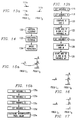
- FIGURE 9 illustrates a processing module indicated generally at 72' and constructed according to the teachings of the present invention.
- Processing module 72' may comprise first and second video processors 80 and 82, line delay 84, and first, second, and third field delays 86, 88, and 90.
- First and second video processors 80 and 82 may comprise, for example, scanline video processors produced by TEXAS INSTRUMENTS INCORPORATED.
- a digital video signal is coupled to a current field input, labeled Y(0), of first video processor 80 and first field delay 86.
- First field delay 86 is coupled to second field delay 88.
- Second field delay 88 is coupled to a second previous field input, labeled Y(-2), of first video processor 80. In this manner, the appropriate information is provided to first video processor 80 to perform the motion detection function.
- First video processor 80 is coupled to an input, labeled Y0, L0, of second video processor 82. Additionally, the output of first video processor 80 is also coupled to line delay 84. Line delay 84 is coupled to an input labeled Y0, L1 of second video processor 82. Second video processor 82 provides two output lines.
- first video processor 80 uses data from a current field and a second previous field to perform motion detection for Mode A.
- the second previous field is provided to first video processor 80 by first and second field delays 86 and 88.
- the details of the motion detection function are set forth below.
- the proscan function is completed by processing module 72' of FIGURE 9 by performing the spatial filtering, interpolation and vertical scaling functions in second video processor 82. The details of the spatial filtering, interpolation and vertical scaling functions are set forth below.
- FIGURE 10 illustrates a processing module indicated generally at 72'' and constructed according to the teachings of the present invention.
- Processing module 72'' may comprise first and second video processors 92 and 94, first and second line delays 96 and 98 and first, second, and third field delays 100, 102 and 104.
- First and second video processors 92 and 94 may comprise, for example, scanline video processors produced by TEXAS INSTRUMENTS INCORPORATED.
- a digital video signal is coupled to a current field input, labeled Y(0), of first video processor 92 and first field delay 100.
- First field delay 100 is coupled to a previous field input, labeled Y(-1), of first video processor 92 and second field delay 102.
- Second field delay 102 is coupled to a second previous field input, labeled Y(-2), of first video processor 92 and third field delay 104.
- Third field delay 104 is coupled to a third previous field, labeled Y(-3), input of first video processor 92. In this manner, the appropriate information is provided to first video processor 92 to perform the motion detection, spatial filtering, and interpolation functions.
- First video processor 92 provides two lines of output for each line in a video field.
- the two lines output by first video processor 92 are coupled to two inputs, namely L0' and L1', of second video processor 94. Additionally, the two lines output by first video processor 92 are coupled to first and second line delays 96 and 98 respectively. First and second line delays 96 and 98 are coupled to inputs L0 and L1 of second video processor 94.
- Second video processor 94 provides two output lines.
- first video processor 92 uses data from a current field and three previous fields to perform motion detection, spatial filtering, and interpolation as called for by Mode B. These fields are provided to first video processor 92 by first, second and third field delays 100, 102, and 104. The details of these functions are set forth below.
- the proscan function is completed by processing module 72'' of FIGURE 10 by performing the vertical scaling function in second video processor 94. The details of the vertical scaling function are also set forth below.
- Motion detection may be performed in both Mode A and Mode B. However, each mode may perform this motion detection in a different manner.
- the output of the motion detection function may be used to determine a factor, referred to as a "k" factor, for each pixel in a video field.
- the ultimate k factor for each pixel may be used in the interpolation function detailed below to convert a video field into a video frame by filling in the missing lines.
- Mode A the output of this motion detection function is further refined to provide the k factor by the temporal motion and spatial filtering functions detailed below.
- mode B the output of this motion detection function is modified to provide the k factor by the spatial filtering function.
- FIGURE 11a illustrates the relationship between the pixels used by the motion detection function according to Mode A.
- the motion detection function takes the difference between the value of a neighboring pixel 106a in a current field and a value of the same pixel 106b in a second previous field to detect motion for a pixel 108.
- the output of the motion detection function may be referred to as MD.
- the motion detection function may be performed in processing module 72'' of FIGURE 9.
- FIGURE 11b is a flow chart for performing the motion detection function according to mode A.
- a variable A is set to the value of a pixel 106a of FIGURE 11a for a current video field.
- the method of FIGURE 11b proceeds to block 109b wherein a variable b is set to the value of pixel 106b of FIGURE 11a.
- the value of pixel 106b is provided to first video processor 80 by first and second field delays 86 and 88 and corresponds to the second previous field of pixel 106a.
- first video processor 80 the value of variable B is subtracted from the value of variable A at Block 109c. Finally, the result of the subtraction step is stored in a variable MD inverse video processor 80 at block 109d.
- FIGURE 12a illustrates the pixels used by the motion detection function according to mode B.
- the output of the motion detection function for pixel 110a is a weighted average of three differences.
- the motion detection output, MD may be calculated according to equation (11): MD 11
- the term is the difference between the value of a first neighboring pixel 112a in a first previous field and the same pixel 112b in a third previous field.
- the term is the difference between a value of a second neighboring pixel 114a in a first previous field and the same pixel 114b in a third previous field.
- the term is the difference between the value of pixel 110b in the current field and the value of the same pixel 110c in a second previous field.
- FIGURE 12b is a flow chart for performing the motion detection function of Mode B.
- the motion detection function of Mode B may be performed in processing module 72''.
- first video processor 92 the value of a variable A1 is set to the value of pixel 112a of FIGURE 12a at block 115a.
- the value of pixel 112a is provided to first video processor 92 by first field delay 100.
- the method proceeds to block 115b wherein a variable A2 is set to the value of pixel 112b of FIGURE 12a.
- the value of pixel 112b is provided to first video processor 92 by first, second, and third field delays 100, 102 and 104.
- a variable B1 of first video processor 92 is set to the value of pixel 114a of FIGURE 112a.
- the value of pixel 114a is provided to first video processor 92 by first field delay 100.
- the method proceeds to block 115d wherein a variable B2 is set to the value of pixel 114b.
- the value of pixel of 114b is provided to first video processor 92 by first, second, and third field delays 100, 102, and 104.
- a variable C1 of first video processor 92 is set to the value of pixel 110b of FIGURE 12a.
- a variable C2 is set to the value of pixel 110c of the FIGURE 112a.
- the value of peel 110c is provided to first video processor 92 by first and second field delays 100 and 102.
- the value of variable A1 is subtracted from the value of variable A2 in first video processor 92.
- the result at the subtraction operation is stored in a variable A.
- the value of variable of B1 is subtracted from the variable of B2.
- the result of the subtraction operation is stored in variable B of first video processor 92.
- the value of variable C1 is subtracted from the value of variable C2.
- the result of the subtraction operation is stored in variable C of first video processor 92.
- a value for the motion detection function, MD is calculated in first video processor 92 according to equation (11).
- Temporal motion detection may be used in Mode A to further refine the output of the motion detection function for each pixel by checking for motion occurring around the pixel of interest as shown in FIGURES 13a and 13b.
- FIGURE 13a illustrates the peels used by the temporal motion detection function.
- FIGURE 13b is a flow chart for performing temporal motion detection according to the teachings of the present invention to determine an output MT. The method of FIGURE 13b begins at block 116 by setting the value of a variable C in second processing module 82 of FIGURE 9 to the output of the motion detection function of FIGURES 11a and 11b for a pixel 111C of the current field.
- the method proceeds to block 118 wherein the value of a variable B is set to the motion detection value for pixel 111b of FIGURE 13a of a first previous field.
- the value of pixel 111b is provided to second video processor by third field delay 90.
- the value of variable B and the value of variable C are compared in second video processor 82.
- the maximum of the value of variable B and the value of variable C is stored in variable M of second video processor 82 at block 122.
- a variable A is set to the motion detection value for pixel 111a of FIGURE 13a in the first previous field.
- the value of pixel 111a is provided to second video processor by line delay 84.
- variable A is compared with the value of variable M in second video processor 82.
- the maximum of variable A and variable M is stored in variable MT in second video processor 82. Therefore, the variable of MT represents the output of the temporal motion function.
- the output of the motion detection functions may be filtered before being used in the interpolation function. Consequently, the output of the motion detection functions may be filtered in both the horizontal and vertical planes to reduce the effects of noise in system 10 of FIGURE 1.
- FIGURE 14 is a flow chart for performing spatial filtering of MD or MT to produce the k factor according to the teachings of the present invention.
- the spatial filtering function may be performed on MT in second video processor 82 of FIGURE 9.
- the spatial filtering function may be performed on MD by first video processor 92 of FIGURE 10.
- the method begins at block 130 wherein MD or MT is filtered in the vertical plane.
- MD or MT may be provided to a vertical low pass filter.
- the vertical low pass filter may, for example, implement a 5 tap vertical low pass filter.
- MD1 (1/4H ⁇ 2 + 1/2H ⁇ 1 + 1/2+1/2H + 1/4H2) * MD 12
- the output of the vertical low pass filter may be a weighted average of the pixel in question, the two pixels above it in the same field, and the two pixels below it in the same field.
- the output of vertical filtering step is filtered in the horizontal plane.
- the output of the vertical low pass filtering may be provided to a horizontal low pass filter.
- the horizontal low pass filter may comprise, for example, a 9 tap horizontal low pass filter.
- a single field of video signal is converted into an entire frame of data using the interpolation function.
- Three interpolation functions may be used in both Mode A and Mode B.
- the three interpolation functions are referred to as motion adaptive line doubling and line averaging.
- the specific interpolation function used may be based on the video signal being processed as shown in Table 4 below.
- the interpolation functions may be implemented in second video processor 82 of FIGURE 9 or first video processor 92 of FIGURE 10. TABLE 4 Video Signal Interpolation Method R, G and B Motion adaptive Y Motion adaptive Pr, Pb or I, Q or U, V Line Averaging or Line Doubling
- FIGUREs 15a and 15b illustrate the motion adaptive interpolation function according to the teachings of the present invention.
- FIGURE 15a illustrates the pixels used to perform the motion adaptive function.
- FIGURE 15b is a flow chart of a method for performing the motion adaptive function.
- the motion adaptive function determines a value for pixel X based on pixels B and C in adjacent lines of the current field and pixel A in the same position as pixel X, but in the previous field as shown in FIGURE 15a.
- Equation (14) may be implemented according to the flow chart of FIGURE 15b.
- the method of FIGURE 15b begins at block 135a wherein a variable K is set to the k factor output of the spatial filtering function for a particular pixel at block 135a.
- the method proceeds to block 135b wherein a variable A is set to the value of pixel A of FIGURE 15a.
- a variable B is set to the value of pixel B of FIGURE 15a.
- the value of a variable C is set to the value of pixel C of FIGURE 15a.
- an interpolated pixel value is calculated according to equation (14).
- the method of FIGURE 15b may be performed in second video processor 82 of FIGURE 9 or first video processor 92 of FIGURE 10.
- FIGURE 16 illustrates the line averaging interpolation function according to the teachings of the present invention.
- the line averaging interpolation function determines a value for pixel X based on pixels B and C in adjacent lines of the current field.
- FIGURE 17 illustrates the line doubling function according to the teachings of the present invention.
- the vertical dimension of a video frame may be expanded or contracted by the vertical scaling function.
- Two methods of vertical scaling are provided for use in Mode B. The two methods are referred to as bilinear and cubic interpolation.
- the vertical scaling function may be used to expand a video frame to use a larger portion of displays 26a through 26c of FIGURE 1.
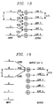
- FIGURE 18 illustrates bilinear interpolation for scaling three lines of input video signal into four lines of output video signal according to the teachings of the present invention.
- the three input lines are designated as line A through line C.
- the four output lines are designated as line 0 through line 3.
- Line A through line C may be scaled to produce line 0 through line 3 with a small contribution from line D according to equations (17a) through (17d):
- Line 0 A ( 17a )
- Line 1 2/8A + 6/8B ( 17b )
- Line 2 4/8B + 4/8C ( 17c )
- Line 3 6/8C + 2/8D ( 17d )
- the next three lines of input video signal may also be scaled to four output video lines according to equations (17a) through (17a).
- the bilinear scaling function of equations (17a) through (17d) may be repeatedly applied to the remaining input lines to produce corresponding sets of output lines.
- nine lines of input video signal may be converted to ten lines of video output according to equations (18a) through (18j) below:
- Line 0 A (18a)
- Line 1 0.1A + 0.9B (18b)
- Line 2 0.2B + 0.8C (18c)
- Line 3 0.3C + 0.7D (18d)
- Line 4 0.4D + 0.6E (18e)
- Line 5 0.5E + 0.5F (18f)
- Line 6 0.6F + 0.4G (18g)
- Line 7 0.7g + 0.3H (18h)
- Line 8 0.8H + 0.2I (18i)
- Line 9 0.9I + 0.1J (18j)
- the input video lines are referred to as line A through line J.
- the output video lines are referred to as line 0 through line 9.
- equations (18a) through (18j) may be repeatedly applied to the remaining input lines to produce corresponding sets of output lines.
- FIGUREs 19 and 20 illustrate cubic interpolation for scaling three lines of input video signal into four lines of output video signal according to the teachings of the present invention.
- the three input lines are designated as line B through line D.
- the four output lines are designated as line 0 through line 3.
- Line B through line D may be scaled to produce line 0 through line 3 with small contributions from line A, line E, and line F according to equations (19a) through (19d):
- Line 0 0.055A + 0.89B + 0.055C (19a)
- Line 1 -0.014609A+0.255078B + 0.782734C - 0.023203D
- Line 2 -0.034375B + 0.534375C + 0.534375D - 0.034375E (19c)
- Line 3 -0.023203C + 0.782734D + 0.255078E - 0.014609F (19d)
- the next three lines of input video signal may also be scaled to four output video lines according to equations (19a) through (19d).
- the cubic scaling function of equations (19a) through (19d) may be repeatedly applied to the remaining input lines to produce corresponding sets of output lines.
- the output video lines are referred to as line 0 through line 9. Beginning with line J, the next nine lines of input video signal may also be scaled to ten output video lines according to equations (20a) through (20j). The cubic scaling function of equations (20a) through (20j) may be repeatedly applied to the remaining input lines to produce corresponding sets of output lines.
- System 10 of FIGURE 1 allows for various qualities of a video picture displayed on displays 26a through 26c to be controlled by user input.
- a user of system 10 may control such picture qualities as sharpness, contrast, brightness, hue and saturation.
- Saturation and hue may, for example, be controlled in first or second matrix multiplication circuit 64 or 66 of FIGURE 7.
- Brightness and contrast may, for example, be controlled in second look up table 70 of FIGURE 7.
- saturation may, for example, be controlled in processing modules 72a through 72c of FIGURE 7.
- FIGUREs 21a through 21d are flow charts illustrating different methods for performing the various picture quality control functions according to the teachings of the present invention. The various methods differ in the order and color space in which the picture quality control functions are performed. FIGUREs 21a through 21d will be described with respect to channel signal processor 22 ⁇ of FIGURE 7.
- the method of FIGURE 21a begins by performing the progressive scan function at block 136 in a color difference color space in processing modules 72a through 72c.
- the sharpness function is performed on the Y video signal by, for example, processing module 72a at block 138.
- the hue control function is performed on the Pr and Pb video signals by second matrix multiplication circuit 66.
- the saturation control function is performed on the Pr and Pb video signals by second matrix multiplication circuit 66.
- the video signal is converted from the color difference color space to the R-G-B color space by second matrix multiplication circuit 66 at block 144.
- the gamma correction function is performed on the R, G, and B video signals in second look up table 70 at block 146.
- the contrast function is performed on the R, G, and B video signals in second look up table 70.
- the brightness function is performed on the R, G, and B video signals in second look up table 70 at block 150.
- the method of FIGURE 21b begins by performing a color space conversion at block 152 in first matrix multiplication circuit 64.
- the method proceeds to block 154 wherein the progressive scan function is performed in the color difference color space in processing modules 72a through 72c.
- the sharpness function is performed on the Y video signal by, for example, processing module 72a at block 156.
- the hue control function is performed on the Pr and Pb video signals by second matrix multiplication circuit 66.
- the saturation control function is performed on the Pr and Pb video signals by second matrix multiplication circuit 66.
- the video signal is converted from the color difference color space to the R-G-B color space by second matrix multiplication circuit 66 at block 162.
- the gamma correction function is performed on the R, G, and B video signals in second look up table 70 at block 164.
- the contrast function is performed on the R, G, and B video signals in second look up table 70.
- the brightness function is performed on the R, G, and B video signals in second look up table 70 at block 168.
- the method of FIGURE 21c begins by performing the hue control function on the Pr and Pb video signals in first matrix multiplication circuit 64 at block 170.
- the saturation control function is performed on the Pr and Pb video signals by first matrix multiplication circuit 64.
- the video signal is converted from the color difference color space to the R-G-B color space for processing in processing modules 72a through 72c by first matrix multiplication circuit 64 at block 174.
- the gamma correction function is performed on the R, G, and B video signals in first look up table 68 at block 176.
- the progressive scan function is performed by processing modules 72a through 72c at block 178.
- the sharpness function is performed on the R, G and B of the video signal by processing module 72 at block 180.
- the contrast function is performed on the R, G, and B video signals in second look up table 70.
- the brightness function is performed on the R, G, and B video signals in second look up table 70 of block 184.
- the method of FIGURE 21d begins by performing the hue control function on the R, G, and B video signals in first matrix multiplication circuit 60 at block 186.
- the saturation control function is performed on the R, G, and B video signals by first matrix multiplication circuit 64.
- the gamma correction function is performed on the R-G-B video signals in first look up table 68.
- the progressive scan function is performed in the R-G-B color space in processing modules 72a through 72c at block 192.
- the sharpness function is performed on the R, G and B video signals by processing modules 72a through 72c at block 194.
- the contrast function is performed on the R, G, and B video signals in second look up table 70.
- the brightness function is performed on the R, G, and B video signals in second look up table 70 at block 198.
- the hue function allows a user to make adjustments to the color of the video picture by a hue control input.
- the hue function may operate in either the color difference or R-G-B color space.
- the hue function may adjust video signals, such as Pr and Pb, in the color difference color space.
- the hue function may adjust R, G, and B video signals in the R-G-B color space.
- the hue control input may comprise an absolute value, X, and a sign value, S.
- the hue function may, for example, be operable to provide 256 adjustment levels in response to an eight bit X input.
- the output of the hue function may be determined according to equation (21a):
- the output of the hue function may be determined according to equation (21b): The value for the variables A through I in equation 21(b) may vary depending on the color space from which the R, G, and B signals were derived.
- the symbols B-Y and R-Y refer to color difference signals in the R-G-B color space.
- the symbols Pr and Pb refer to color difference signals in a color difference color space.
- a vector representing the two color difference signals is rotated in the plane of FIGURE 22.
- the amount and direction of rotation of the input hue vector is controlled by the X and S values of the hue control input.
- the result of the hue control function is an output vector 202.
- the saturation function allows a user to make adjustments to the color of the video picture by a saturation control input.
- the saturation function may operate in either the color difference or R-G-B color space.
- the saturation function may adjust video signals, such as Pr and Pb, in the color difference color space.
- the saturation function may adjust the R, G, and B video signals in the R-G-B color space.
- the saturation control input may comprise an absolute value, X, and a sign value, S.
- the saturation function may, for example, be operable to provide 256 adjustment levels in response to an eight bit X input.
- the output of the saturation function is also determined according to equation (21a).
- the output of the saturation function is determined according to equation (21b).
- the value for the variables A through I in equation (21b) may vary depending on the color space from which the R, G, and B signals were converted.
- the symbols B-Y and R-Y refer to color difference signals in the Y, R-Y, B-Y space.
- the symbols Pr and Pb refer to the color difference signals in the SMPTE 240M color difference color space.
- a magnitude of a vector 204 representing the color difference signals is varied in the plane of FIGURE 23.
- the amount and direction of change in the magnitude of the input saturation vector is controlled by the X and S values of the saturation control input.
- the result of the saturation control function is an output vector 206.
- the sharpness function allows a user to make adjustments to a video picture by a sharpness control input.
- the sharpness function may operate in either the color difference or R-G-B color space.
- the sharpness function may adjust the luma, Y, video signal in the color difference color space.
- the sharpness function may adjust the R, G, and B video signals in the R-G-B color space.
- the sharpness control input may comprise an absolute value, X, and a sign value, S.
- the sharpness function may, for example, be operable to provide 256 adjustment levels in response to an eight bit X input.
- FIGURE 24 is a flow chart that illustrates the operation of the sharpness function according to the teachings of the present invention.
- the sharpness function may be implemented in processing modules 72a through 72c of FIGURE 7. In a color difference color space, the sharpness function only operates on the Y video signal. In the R-G-B color space, the sharpness function may operate on each of the R, G, and B video signals.
- appropriate video signals may be filtered in a high pass filter.
- the values of A, B, C, D, and E in equation (22) correspond to the Y values for the pixels shown in FIGURE 25.
- equation (22) may be applied to pixel A of FIGURE 25 for each video signal R, G, and B.
- the output of the high pass filter is multiplied by the value X of the sharpness control input.
- a decision is made at block 212 as to whether the value of S indicates a positive or a negative sharpness control input. If the value S of the sharpness control input corresponds to a positive sharpness control input, the result of the multiplication is added to the original video signals at block 214. Otherwise, the result of the multiplication is subtracted from the original video signals at block 216.
- the outputs of this operation are sharpness adjusted video signals.
- the contrast function allows a user to make adjustments to the color in the R-G-B color space of the video picture by a contrast control input.
- the contrast control input may comprise an absolute value, X, and a sign value, S.
- the contrast function may, for example, be operable to provide 256 adjustment levels in response to an eight bit X input.
- FIGURE 26 is a flow chart that illustrates the operation of the contrast function according to the teachings of the present invention.
- the contrast function may be implemented in second look up table 70 of FIGURE 7.
- the three video signals in the R-G-B color space may be provided to a multiplier to multiply the video signals by the value X.
- a decision is made as to whether the value of S indicates a positive or a negative contrast control input.
- the output of the multiplier is added to the original video signals at block 222 if the value of S corresponds to a positive contrast control input. Alternatively, the output of the multiplier is subtracted from the original video signals if S is negative at block 224.
- FIGURE 27 graphs an input R, G, or B video signal against an output R ⁇ , G ⁇ , or B ⁇ video signal.
- the contrast control input alters the slope of the output/input curve.
- the brightness function allows a user to make adjustments to the color in the R-G-B color space of the video picture by a brightness control input.
- the brightness control input may comprise an absolute value, X, and a sign value, S.
- the brightness function may, for example, be operable to provide 256 adjustment levels in response to an eight bit X input.
- the brightness function may be implemented in second look up table 70 of FIGURE 7. If the S value corresponds to a positive brightness control input, the brightness function adds X to each video signal, R, G, and B. Alternatively, the brightness function subtracts X from each video signal.
- the brightness function shifts the input/output curve such that the output is greater or less than the input by the value X.
- FIGURE 29 illustrates an embodiment of a formatter indicated generally at 24 ⁇ and constructed according to the teachings of the present invention.
- One formatter 24 ⁇ of the type illustrated in FIGURE 29 may be used for each of formatters 24a through 24c of FIGURE 1.
- formatter 24 ⁇ will be described in terms of formatter 24a of FIGURE 1. It is understood that formatter 24 ⁇ is not so limited, but may be used for formatters 24b and 24c as well.
- Formatter 24 ⁇ comprises line segment mapper 226 and data format unit 228.
- Line segment mapper 226 is coupled to two output lines from each channel signal processor 22a through 22d of FIGURE 1.
- line segment mapper 226 may be coupled to the two output lines corresponding to the red video signal from each channel signal processor 22a through 22d.
- Line segment mapper 226 is coupled to provide a number of outputs equal to the number of inputs to data format unit 228.
- Data format unit 228 provides four 32 bit output signals to display 26 of FIGURE 1.
- line segment mapper 226 receives processed video data for one of the video signals, such as, for example, the red video signal.
- the video signals received from channel signal processors 22a through 22d of FIGURE 1 contain some overlap due to the manner in which line slicer 14 divides the input video signals as described previously with respect to FIGURE 1.
- Line segment mapper 226 operates to remove the overlap in the various channels caused by line slicer 14.
- the video signal is formatted, for example, for display 26a of FIGURE 1 by data format unit 228.
- data format unit 228 may create a series of bit planes wherein one bit of data in each bit plane corresponds to each pixel of display 26. Data format unit 228 may provide these bit planes to display 216 in 128 bit words as described below.
- FIGURE 30 illustrates an embodiment of a data format unit indicated generally at 228 ⁇ and constructed according to the teachings of the present invention.
- Data format unit 228 comprises buffer memory 230 and a plurality of multiplexers 232.
- Plurality of multiplexers 232 may comprise, for example, 128 multiplexers controlled by a bit select signal from timing and control circuit 28 of FIGURE 1.
- Buffer memory 230 is coupled to eight 10 bit outputs of line segment mapper 226 of FIGURE 29.
- Buffer memory 230 comprises a plurality of memory locations 234 equal in number to the number of pixels in a single line of video signal.
- Memory locations 234 may, for example, be oriented in 16 rows, each comprising 128 columns.
- Each multiplexer 232 may be coupled to an output of buffer memory 230 corresponding to a column of memory locations 234.
- individual lines of video signal may be sequentially received and stored in memory locations 234 of buffer memory 230.
- Each memory location 234 comprises 10 bits of video data for one pixel in a single line of a video frame.
- the video data may be communicated to display 26a of FIGURE 1 one line at a time to form 10 bit planes.
- a bit plane corresponds to one bit of data for each pixel in a video frame. Therefore, the first bit plane, for example, may correspond to the most significant bit for each pixel and the tenth bit plane may correspond to the least significant bit for each pixel.
- data format unit 228 ⁇ may create the first line of the appropriate bit planes.
- Data format unit may communicate the first line of the ten bit planes in 128 bit words to display 26a of FIGURE 1.
- the first 128 bit word used in forming the first line of the first bit plane may correspond to the bottom row of memory locations 234 of buffer memory 230.
- the first bit of each memory location 234 in successive rows of buffer memory 230 may be used to create successive 128 bit words to fill out the first line of the first bit plane.
- the first line of a first bit plane is complete once all of the first bits stored in all of the rows of memory locations 234 have been used.
- This process may be repeated for successive bits in each memory location 234 until all of the data for a single line of video signal has been communicated to display 26 of FIGURE 1. Thereby, the first line of each of the 10 bit planes of data for a single frame of video signal are communicated to display 26 of FIGURE 1. The remaining lines of each of the ten bit planes associated with a frame of video may be communicated to display 26a of FIGURE 1 by repeating the above process for each line in the video frame.
- FIGURE 31 illustrates an embodiment of a display indicated generally at 26 ⁇ and constructed according to the teachings of the present invention.
- One display 26 ⁇ of the type illustrated in FIGURE 31 may be used for each display 26a through 26c of FIGURE 1.
- display 26 ⁇ will be described with respect to display 26a. It is understood that display 26 ⁇ is not so limited, but may also be used for displays 26b and 26c.
- Display 26 ⁇ comprises an SLM 236, and a plurality of Video Random Access Memories (hereinafter "VRAMs") 238.
- SLM 236 may comprise, for example, a 2 x 128 pin DMD produced by TEXAS INSTRUMENTS INCORPORATED or other appropriate display unit.
- a DMD is a monolithic, micromechanical spatial light modulator having a plurality of pixels.
- a DMD may integrate discrete, tilting mirror elements with MOS addressing circuits at each pixel.
- the tilting mirror may be tilted to one of two appropriate binary positions by use of electrostatic attraction. In a first position, the tilting mirror of a particular pixel may reflect red, green or blue light, for example, at a display screen corresponding to the appropriate color at that pixel. In a second position, the tilting mirror of a particular pixel may not reflect any light at a display screen corresponding to a black pixel. Color shades may be obtained by controlling the amount of time a mirror corresponding to a particular pixel is in the first position.
- a DMD may, for example, be provided with appropriate mirrors to provide 2048 by 1152 pixels.
- a plurality of VRAMs 238 may be coupled to receive video data corresponding to a video signal, for example, the red video signal, in 128 bit words from data format unit 228 of FIGURE 30 as described above.
- Four individual VRAMs 238 may be coupled to each of four channels of SLM 236.
- Each channel of SLM 236 may have a width of 512 pixels in each channel.
- Two VRAMs 238 may be coupled to a first half of each channel of SLM 236 and two VRAMs 238 may be coupled to a second half of SLM 236.
- VRAMs 238 store and communicate successive sets of 10 bit planes to SLM 236.
- SLM 236 may reflect, for example, red light from an appropriate light source (not explicitly shown) at a screen (not explicitly shown) so as to display video images corresponding to the processed video data.
- the amount of light reflected by SLM 236 for a particular frame of video may be controlled by the 10 bit planes stored in VRAMs 238.
- a bright red color may be reflected by a particular pixel of SLM 236 by tilting the mirror for that pixel to the first, or reflecting, position for the length of time corresponding to a video frame.
- the brightness of the pixel may be varied by controlling the time that the mirror is in the first position.
- each mirror may be controlled by the 10 bit planes of VRAMs 238.
- each bit plane may control the binary location of each mirror for a portion of the time corresponding to a video frame.
- the bit plane corresponding to the most significant bit may control SLM 236 for one-half of the time corresponding to a video frame.
- Each successive bit plane may then control SLM 236 for decreasing amounts of time in proportion to the position of the bits of that bit plane in the original 10 bit word corresponding to each pixel.
- SLM 236 may display appropriate video images.
- the combination of the red, green and blue light reflected by displays 26a through 26c of FIGURE 1 results in the display of the processed video signal.
Abstract
Description
- This invention relates in general to the field of electronic devices. More particularly, this invention relates to a digital television system.
- Standard television has not kept up with the modern electronic revolution as exemplified by the recent developments in the personal computer industry. Consequently, a standard television system does not produce as high a quality picture as one might expect given the recent advancements seen in other modern electronic systems.
- Standard television systems may receive and display analog, rather than digital, video signals. A typical standard video signal is referred to as an "interlaced" video signal. This means that each frame of video data displayed on the standard system is divided into two fields. The first field may, for example, contain the odd lines of the video frame. The second field may contain the even lines of the same video frame. The two fields making up the single frame are received and displayed successively on the standard system and may appear to a viewer as a single frame. Dividing and displaying a video frame in this manner may decrease the quality of the output of a video system.
- Additionally, a standard television system may include an analog display such as a cathode ray tube (hereinafter "CRT"). Because a CRT is an analog device that does not provide a linear response to an input signal, a "gamma curve" is introduced into a standard video signal to compensate for the non-linearity of the CRT. Standard video signals therefore are not directly compatible with a linear digital display.
- Furthermore, a standard television system may not be operable to process a video signal prior to displaying the video signal. Similarly, a standard television system may not be programmable to operate on a number of different standard video signals. Finally, a standard television system may be limited to a small display area on the order of 640 by 480 pixels.
- In accordance with the present invention, a digital television system is provided which substantially eliminates or reduces disadvantages and problems associated with prior systems. The teachings of the present invention provide a digital television system that processes video signals in a parallel architecture. A parallel architecture has not been previously used in a television system.
- More specifically, the present invention provides a digital television system that may process input video signals in various forms. The system comprises circuitry that is operable to divide a line of input video signals into a plurality of channels for each input video signal. The channels of input video signals are processed in parallel. The processed video signals may be displayed on a display.
- It is a technical advantage of the present invention to provide a digital television system that processes a video signal in a plurality of parallel channels. The channels of the system may correspond to vertical strips of a video frame. Each channel may contain an overlap of, for example, one to five pixels with an adjacent channel. The overlap between channels may allow identical horizontal processing of pixels on the ends of each channel. The overlapping pixels may be removed before the processed video signal is displayed such that redundant pixels are not displayed.
- It is another technical advantage of the present invention to provide a digital television system that is operable to convert a standard video signal into a non-interlaced video signal. The system may convert each field of an interlaced video signal into a non-interlaced frame. Additionally, the system may remove the effect of a standard gamma curve from a standard video signal.
- It is another technical advantage of the present invention to provide a digital television system including a digital display such as a spatial light modulator. The display may provide 2X intensity levels in response to X bit planes formed for each of the video signals from video data for each pixel in a video frame. The first bit plane for each input video signal, corresponding to the most significant bit for each pixel, may control the display for one-half of the time for one frame. Successive bit planes may each control the display for a period of time proportionate to the position of the bits of that bit plane in the pixels making up that bit plane.
- It is a technical advantage of the present invention to provide a programmable digital television system. The system may be programmed by a user to process a particular standard video signal. Additionally, the system may be programmed to implement various functions to produce a high definition display from a standard video signal input.
- It is another technical advantage of the present invention to provide a digital television system that is operable to process red, green and blue video signals or a luminance video signal and two color difference video signals.
- It is another technical advantage of the present invention to provide a digital television system that is operable to modify the size of a video frame. The system may expand the pixel width of a video frame by controlling the rate at which a line of video data is sampled. Additionally, the system may scale the number of lines in a video frame.
- It is another technical advantage of the present invention to provide a digital television system with a large display area on the order of 2048 by 1152 pixels.
-
- For a more complete understanding of the present invention and the advantages thereof, reference is now made to the following description taken in conjunction with the accompanying drawings in which like reference numbers indicate like features and wherein:
- FIGURE 1 illustrates a digital television system constructed according to the teachings of the present invention;
- FIGURE 2 illustrates four vertical strips created by the system of FIGURE 1;
- FIGURE 3 illustrates the overlap in pixels between adjacent channels created by the system of FIGURE 1;
- FIGURE 4 illustrates an embodiment of the composite video interface and separation circuit of FIGURE 1 constructed according to the teaching of the present invention;
- FIGURE 5 illustrates an embodiment of the analog to digital converter circuit of FIGURE 1 constructed according to the teachings of the present invention;
- FIGURE 6 illustrates an embodiment of the line slicer of FIGURE 1 constructed according to the teaching of the present invention;
- FIGURE 7 illustrates an embodiment of a channel signal process of FIGURE 1 constructed according to the teachings of the present invention;
- FIGURE 8 illustrates a gamma correction function according to the teachings of the present invention;
- FIGURE 9 illustrates an embodiment of a processing module of FIGURE 7 constructed according to the teachings of the present invention;
- FIGURE 10 illustrates another embodiment of a processing module of FIGURE 7 constructed according to the teachings of the present invention;
- FIGURE 11a illustrates the relationship between the pixels used by a motion detection function according to the teachings of the present invention;
- FIGURE 11b is a flow chart for performing a motion detection function according to the teachings of the present invention;
- FIGURE 12a illustrates the relationship between the pixels used by a motion detection function according to the teachings of the present invention;
- FIGURE 12b is a flow chart for performing a motion detection function according to the teachings of the present invention;
- FIGURE 13a illustrates the relationship between the pixels used to perform the temporal motion detection function according to the teachings of the present invention;
- FIGURE 13b is a flow chart for performing temporal motion detection according to the teachings of the present invention;
- FIGURE 14 is a flow chart for performing spatial filtering according to the teachings of the present invention;
- FIGURE 15a illustrates a motion adaptive interpolation function according to the teachings of the present invention;
- FIGURE 15b is a flow chart for performing a motion adaptive interpolation function according to the teachings of the present invention;
- FIGURE 16 illustrates a line averaging interpolation function according to the teachings of the present invention;
- FIGURE 17 illustrates a line doubling function according to the teachings of the present invention;
- FIGURE 18 illustrates bilinear interpolation for scaling three lines of input video signal into four lines of output video signal according to the teachings of the present invention;
- FIGUREs 19 and 20 illustrate cubic interpolation for scaling three lines of input video signal to four lines of output video according to the teachings of the present invention;
- FIGURE 21a through 21d are flow charts illustrating various methods for performing picture quality functions according to the teachings of the present invention;
- FIGURE 22 is a graph showing the affect of a hue control input according to the teachings of the present invention;
- FIGURE 23 is a graph showing the affect of a saturation control input according to the teachings of the present invention;
- FIGURE 24 is a flow chart that illustrates the operation of a sharpness function according to the teaching of the present invention;
- FIGURE 25 illustrates a configuration of pixels used in the sharpness function according to the teaching of the present invention;
- FIGURE 26 is a flow chart that illustrates the operation of a contrast function according to the teachings of the present invention;
- FIGURE 27 is a graph illustrating the effect of the contrast function according to the teachings of the present invention;
- FIGURE 28 is a graph illustrating the effect of the brightness function according to the teachings of the present invention;
- FIGURE 29 illustrates an embodiment of a formatter of FIGURE 1 constructed to the teachings of the present invention;
- FIGURE 30 illustrates an embodiment of a data format unit of FIGURE 29 constructed according to the teachings of the present invention; and
- FIGURE 31 illustrates an embodiment of a display of FIGURE 1 constructed according to the teaching of the present invention.
- FIGURE 1 illustrates a digital television system indicated generally at 10 and constructed according to the teachings of the present invention.
System 10 comprises a parallel architecture wherein input video signals may be divided into channels to be processed in parallel. For example,system 10 may implement appropriate functions such that a standard video signal may be used to provide a high definition video display. Alternatively,system 10 may sample and display a high definition video signal. -
System 10 may receive video signals in composite or component form. For example,system 10 may receive an analog composite video signal, an analog video signal in component form, or a digital video signal.System 10 may convert a composite video signal into a plurality of video signals for processing. For example, an analog composite video signal in the format established by the National Television Standards Committee (hereinafter "NTSC") may be separated into a luminance signal, identified by the symbol Y, and two color difference signals, identified by the symbols I and Q. Alternatively,system 10 may separate other standard composite video signals into appropriate video signals for processing according to Table 1 below.TABLE 1 Input Video Format Color Space Domain NTSC Y, I, Q PAL and SECAM Y, U, V SMPTE 240M, SMPTE 260M Y, Pr, Pb
It is noted that the other standard video formats include: Phase Alternating Line, hereinafter "PAL"; Sequential Color with Memory, hereinafter "SECAM"; and Society of Motion Picture Engineers, hereinafter "SMPTE". - Each of these standard video signals comprise a luminance signal, hereinafter "luma" or "Y", and a chrominance signal, hereinafter "chroma" or "C". The chroma signal may be further divided into appropriate color difference signals as shown in Table 1. For clarity, each of the standard video signals may hereinafter be referred to as providing a video signal in a "color difference color space" or a "Y-I-Q color space." As an alternative to the standard video signals of Table 1, a video source may be coupled to
system 10 to provide a red video signal, hereinafter "R", a green video signal, hereinafter "G", and a blue video signal, hereinafter "B". Such a video source may hereinafter be referred to as providing a video signal in an "R-G-B color space." -
System 10 prepares a video signal for parallel processing in receivingcircuitry 12, andline slicer 14. Receivingcircuitry 12 may receive, for example, a composite video signal in the NTSC format from an external source (not explicitly shown). Alternatively, receivingcircuitry 12 may receive separate Y and C video signals. Furthermore, receivingcircuitry 12 may receive separate video signals in an R-G-B color space. - Receiving
circuitry 12 comprises composite video interface andseparation circuit 16 coupled to analog todigital converter circuit 18. Composite video interface andseparation circuit 16 may separate a composite video signal into, for example, three separate video signals. Analog todigital converter circuit 18 may convert each of the separate video signals into ten bit digital video signals. Analog todigital converter circuit 18 of receivingcircuitry 12 is coupled to provide three ten bit digital video signals toline slicer 14. Additionally, a digital video signal may be coupled directly toline slicer 14. -
Line slicer 14 divides each digital video signal into a plurality of separate channels for each line of composite video signal. For example,line slicer 14 may divide each digital video signal into four, five or another appropriate number of channels. The number of channels may depend on the number of pixels in a line of video signal, and the number of pixels that may be simultaneously processed by a video signal processor ofsystem 10.Line slicer 14 may provide appropriate overlap between the various channels for processing as described below. -
System 10 processes the digital video signals inprocessing circuitry 20.Processing circuitry 20 is coupled toline slicer 14.Processing circuitry 20 comprises a plurality of channel signal processors 22a through 22d. The number ofchannel signal processors 22 may be equal to the number of channels provided byline slicer 14. Each channel signal processor 22a through 22d receives all three 10 bit digital video signals for the channel corresponding to that signal processor 22a through 22d.Processing circuitry 20 may convert each line of digital video signal into two lines of digital video signal output. Each channel signal processor 22a through 22d, therefore, may have six separate outputs, for example, two ten bit red outputs, two ten bit green outputs, and two ten bit blue outputs. Additionally, processingcircuitry 20 may perform the following functions: color space conversion, gamma correction, and picture quality control which will be described in detail below. -
System 10 reconnects and displays the processed video data. A plurality of formatters 24a through 24c reconnect the video data and a plurality of displays 26a through 26c display the video data. One formatter 24a through 24c and one display 26a through 26c operate on a different digital video signal as indicated in FIGURE 1. For example, formatter 24a and display 26a may operate on a red video signal. Formatter 28b anddisplay 26b may operate on a green video signal. Finally,formatter 24c anddisplay 26c may operate on a blue video signal. - Two ten bit outputs of each channel signal processor 22a through 22d are coupled to an appropriate formatter 24a through 24c. Formatters 24a through 24c remove overlap between adjacent channels, reconnect the channels, and prepare the reconnected digital video signals for display on displays 26a through 26c. Formatters 24a through 24c each provide 128 bit words in four 32 bit channels to displays 26a through 26c. Displays 26a through 26c may comprise, for example, a Spatial Light Modulator (hereinafter "SLM") such as a 2 x 128 pin Digital Micromirror Device (hereinafter "DMD") produced by TEXAS INSTRUMENTS INCORPORATED. However, displays 26a through 26c are not limited to digital displays. It is within the scope of the teachings of the present invention for the processed video signal to be displayed on an analog display.
- Timing and
control circuit 28 is coupled to composite video interface andseparation circuit 16, analog todigital converter circuit 18,line slicer 14, processingcircuitry 20, formatters 24a through 24c, and displays 26a through 26c. Timing andcontrol circuit 28 is operable to control the timing of each aspect ofsystem 10. The timing ofsystem 10 may be accomplished through use of a synchronization (hereinafter "sync") signal supplied to timing andcontrol circuit 28 by composite video interface andseparation circuit 16. Additionally, timing andcontrol circuit 28 is operable to accept user inputs to control the timing of various functions ofsystem 10. For example, timing andcontrol circuit 28 may receive user inputs to select the type of input video signal coupled to receivingcircuitry 12. Furthermore, timing andcontrol circuit 28 may accept information for processingcircuitry 20 such as a scaling factor, a gamma correction factor, the desired processing method, and picture control functions; each of which are described more fully below. Furthermore, timing andcontrol circuit 28 may receive a specific sampling rate for analog todigital converter circuit 18. - In operation,
system 10 may prepare a standard video signal to produce a high definition display. As described previously,system 10 may receive analog or digital video signals in composite or separated form. For conciseness, the operation ofsystem 10 is described in conjunction with receiving an analog composite video signal.System 10 separates a composite video signal into video signals, divides the video signals into a plurality of channels, and processes the channels in parallel. An advantage of using a parallel architecture insystem 10 is thatsystem 10 is able to process the video signals at a low speed while providing a high definition display. Consequently,system 10 may incorporate existing video processor components. - Composite video interface and
separation circuit 16 separates the composite video signal into, for example, three separate video signals. Composite video interface andseparation circuit 16 may, for example, separate a composite video signal into Y, I, and Q video signals of the NTSC standard. - Analog to
digital converter circuit 18 may sample each video signal at a frequency of, for example, 71.1 MHz. The appropriate sampling rate may depend on the number of pixels allocated for a line of video on displays 26a through 26c, and the time for one line of video signal to be received by receivingcircuitry 12. Therefore, the sampling rate may be adjusted to create a predetermined number of pixels for each line of video signal. Analog todigital converter circuit 18 may comprise, for example, Analog to Digital Converter board AD9060 produced by ANALOG DEVICES. Alternatively, analog todigital converter circuit 18 may comprise another appropriate analog to digital converter device operable to sample data at an appropriate sampling rate on the order of 75 MHz. -
Line slicer 14 divides each digital video signal into a plurality of separate channels for each line of video signal. For example,line slicer 14 may divide each line of the digital video signal into four channels so that the video signal may be processed in parallel. By dividing each line of digital video signal in the same manner, each channel signal processor 22a through 22d effectively processes one vertical strip of each video frame. FIGURE 2 shows the four vertical strips processed by channel signal processors 22a through 22d for the embodiment of FIGURE 1. Alternatively,line slicer 14 may divide a line on a pixel by pixel basis orline slicer 14 may divide a video frame into horizontal strips. An advantage of dividing a video frame into vertical strips is that the related processing steps performed by processingcircuitry 20 are simplified. - Additionally,
line slicer 14 may provide for overlap between the vertical channels by providing common pixels to adjacent channels as shown in FIGURE 3. The overlap may comprise, for example, from one to five pixels. The overlapping pixels may be used to provide appropriate data for each channel to perform the various functions described below as called for by processingcircuitry 20. The amount of overlap between channels may be varied depending of the specific functions implemented in processingcircuitry 20. -
System 10 processes the digital video signals inprocessing circuitry 20.Processing circuitry 20 may perform the progressive scan function (hereinafter "proscan"). Proscan "de-interlaces" a video signal by creating an entire video frame from a single or multiple video fields at the field rate. As described previously, a standard video signal may comprise two fields of video data for each frame. Additionally, processingcircuitry 20 may convert the digital video signals into a different color space. For example, processingcircuitry 20 may convert digital video signals from a color difference color space to an R-G-B color space. Furthermore, processing circuitry may remove a gamma curve from a standard video signal. Finally, processingcircuitry 20 may control the quality of a video display in response to user inputs such as inputs for adjustments to brightness, hue, contrast, sharpness and saturation. Each of these functions is described in detail below. -
System 10 reconnects and displays the processed digital video signal using formatters 24a through 24c and displays 26a through 26c. Formatters 24a through 24c remove overlap between adjacent channels. Additionally, formatters 24a through 24c prepare the reconnected digital video signals for display on displays 26a through 26c. For example, formatters 24a through 24c may produce a plurality of bit planes from the reconnected digital video signals. Each bit plane may correspond to a particular bit for each pixel in a particular video frame. In the embodiment of FIGURE 1, formatters 24a through 24c each may produce 10 bit planes of video data for each separate video signal that are to be provided to displays 26a through 26c in 128 bit words. Based on the output of formatters 24a through 24c, displays 26a through 26c may project appropriate images corresponding to the processed video signals on, for example, a screen (not shown). The combination of the different video signals output by displays 24a through 24c result in a single, appropriately colored, image. - It should be understood that
system 10 may be operable to be programmed to accept any appropriate standard analog or digital video signal. Alternatively,system 10 may be preprogrammed to accept only a limited number of appropriate standard analog or digital video signals. - FIGURE 4 illustrates one embodiment of a composite video interface and separation circuit indicated generally at 16¢ and constructed according to the teachings of the present invention. Composite video interface and
separation circuit 16¢ may comprise, for example, Y/C separation circuit 30,luma signal multiplexer 32,chroma signal multiplexer 34,luma processing circuit 36,chroma processing circuit 38,sync signal multiplexer 40,sync separation circuit 42, and first andsecond output multiplexers - A composite video signal may be coupled to composite interface and
separation circuit 16¢ at Y/C separation circuit 30. Y/C separation circuit 30 separates a standard composite video signal into a luma signal, Y, and a chroma signal, C. A Y output of Y/C separation circuit 30 is coupled toluma signal multiplexer 32. Additionally, a separated luma signal is also coupled toluma signal multiplexer 32. A C output of Y/C separation circuit 30 is coupled tochroma signal multiplexer 34. Additionally, a chroma signal is coupled tochroma signal multiplexer 34.Luma signal multiplexer 32 is coupled toluma processing circuit 36 andsync signal multiplexer 40. Additionally, the output ofchroma signal multiplexer 34 is coupled tochroma processing circuit 38. - A refined luma signal is provided to
first output multiplexer 44 byluma processing circuit 36. Additionally, a green video signal, G, is also coupled tofirst output multiplexer 44. The green video signal is also provided to syncsignal multiplexer 40. -
Chroma processing circuit 38 provides two color difference signals tosecond output multiplexer 46. A red video signal, R, and a blue video signal, B, are provided tosecond output multiplexer 46. - Finally, the output of
signal multiplexer 40 is coupled to syncseparation circuit 42. The output of each ofluma signal multiplexer 32,chroma signal multiplexer 34,signal multiplexer 40, and first andsecond output multiplexers control circuit 28 of FIGURE 1. - In operation, a standard video signal, such as the standard video signals shown below in Table 2, may be prepared for processing by
system 10 of FIGURE 1 in composite video interface andseparation circuit 16¢.TABLE 2 Input Video Type Input Format (Interlaced) SMPTE 240 M 1840 X 517 NTSC 640 X 241.5 Wide NTSC # 853 853 X 241.5 NTSC 4.43 640 X 241.5 PAL 768 X 288.5 SECAM 768 X 288.5 Wide PAL # 1024 X 288.5
A composite video signal is separated into Y and C video signals by Y/C separation circuit 30. The separated Y and C video signals may be passed toluma processing circuit 36 andchroma processing circuit 38 respectively byluma signal multiplexer 32 andchroma signal multiplexer 34. -
Luma processing circuit 36 refines the Y video signal input and provides it tofirst output multiplexer 44.First output multiplexer 44 may provide the processed Y video signal to analog todigital converter circuit 18 of FIGURE 1. Similarly,chroma processing circuit 38 converts the C video signal into two appropriate color difference signals, such as I and Q. The output color difference signals are provided tosecond output multiplexer 46.Second output multiplexer 46 may provide the color difference signals to analog todigital converter circuit 18 of FIGURE 1. - Alternatively, composite video interface and
separation circuit 16¢ may provide previously separated Y and C video signals to analog todigital converter circuit 18 of FIGURE 1. A previously separated Y video signal may be provided to analog todigital converter circuit 18 of FIGURE 1 byluma signal multiplexer 32,luma processing circuit 36, andfirst output multiplexer 44. Similarly, a previously separated C video signal may be provided to analog todigital converter circuit 18 of FIGURE 1 bychroma signal multiplexer 34,chroma processing circuit 38 andsecond output multiplexer 46. - Finally, composite video interface and
separation circuit 16¢ may provide component R, G and B signals to analog todigital converter circuit 18 of FIGURE 1. As shown in FIGURE 4, a G video signal is provided directly tofirst output multiplexer 44. Additionally, R and B video signals are provided directly tosecond output multiplexer 46. In response to an appropriate signal from timing andcontrol circuit 28, first andsecond output multiplexers digital converter circuit 18 of FIGURE 1. - Composite video interface and
separation circuit 16¢ may also remove a sync signal from an input video signal. For example,sync signal multiplexer 40 may provide either a Y video signal or a G video signal to syncseparation circuit 42.Sync separation circuit 42 may remove a horizontal sync signal and a vertical sync signal from the video signal.Sync separation circuit 42 may provide the output sync signals to timing andcontrol circuit 28 of FIGURE 1. Timing andcontrol circuit 28 may base the timing of each operation performed insystem 10 on the sync signal removed from the video signal. - FIGURE 5 illustrates an embodiment of an analog to digital converter circuit indicated generally at 18¢ and constructed according to the teachings of the present invention. FIGURE 5 only illustrates one analog to digital converter of analog to
digital converter circuit 18¢. It is understood that analog todigital converter circuit 18 of FIGURE 1 may comprise one analog todigital converter circuit 18¢ illustrated in FIGURE 5 for each separate video signal to be processed bysystem 10 of FIGURE 1. However, for conciseness, analog todigital converter circuit 18¢ will be described herein only in conjunction with the circuitry shown in FIGURE 5 for converting one video signal from an analog signal to a digital signal. - Analog to
digital converter circuit 18¢ comprisesline 47, firstlow pass filter 48, secondlow pass filter 50,multiplexer 52,multiplier 54,adder 56, and A/D converter 58. A separated video signal from composite video interface andseparation circuit 16 of FIGURE 1 is coupled to firstlow pass filter 48, secondlow pass filter 50, andmultiplexer 52. The output of firstlow pass filter 48 and secondlow pass filter 50 are also coupled tomultiplexer 52. The output ofmultiplexer 52 is controlled by a signal from timing andcontrol circuit 28.Multiplexer 52 is coupled tomultiplier 54.Multiplier 54 amplifies the output ofmultiplexer 52 according to a control signal, GAIN ADJ, from timing andcontrol circuit 28.Multiplier 54 is coupled to adder 56.Adder 56 is coupled to A/D converter 58.Adder 56 is also controlled by a signal from timing andcontrol circuit 28. Additionally, an output of A/D converter 58 is coupled to adder 56. - In operation, a video signal is provided to analog to
digital converter circuit 18¢. The video signal may be filtered in firstlow pass filter 48 or secondlow pass filter 50 to prevent aliasing in A/D converter 58. For example, firstlow pass filter 48 may comprise a low pass filter having a roll-off point at 30 MHz or other appropriate frequency for filtering a Y video signal. Additionally, secondlow pass filter 58 may comprise a low pass filter having a roll-off point at 15 MHz or other appropriate frequency for filtering a color difference signal. Alternatively, a video signal may be provided directly tomultiplexer 52 without filtering vialine 47. - Before the video signal is converted to a digital signal, the magnitude of the video signal may be adjusted in
multiplier 54 to scale a voltage of, for example, 0.5 Volts peak-to-peak to the maximum analog input level of A/D converter 58. Additionally, a DC offset may be added inadder 56 to adjust the DC value of the component video signal to a predetermined level. Finally, the component video signal is sampled at an appropriate sampling rate, such as 71.1 MHz in A/D converter 58. The output of A/D converter 58 is provided toline slicer 14 of FIGURE 1. - FIGURE 6 illustrates an embodiment of a line slicer indicated generally at 14¢ and constructed according to the teachings of the present invention. The purpose of
line slicer 14¢ is to divide each digital video signal into a plurality of separate channels for each line of composite video signal such thatsystem 10 may process the separate channels in parallel.Line slicer 14¢ comprisesmultiplexer 59, slow downlogic circuit 60, and a plurality of first in-firstout buffer memories 62. -
Multiplexer 59 receives input forline slicer 14¢.Multiplexer 59 is coupled to analog todigital converter 18 of FIGURE 1. Analog todigital converter 18 may provide digital video signals in a Y-I-Q color space or an R-G-B color space. Additionally,multiplexer 59 is coupled to receive digital video signals in either the Y-I-Q or R-G-B color space. For example,multiplexer 59 may be coupled to receive digital video signals in the SMPTE 260M format.Multiplexer 59 is coupled to slow downlogic 60. The output ofmultiplexer 59 is controlled by a signal from timing andcontrol circuit 28. - Slow down
logic 60 compensates for a difference in speed between analog todigital converter 18 and first in-firstout buffer memories 62 as described below.Multiplexer 59 provides three separate video signals to slow downlogic circuit 60. For example, analog todigital converter circuit 18 may provide Y, I, and Q video signals to slow downlogic circuit 60. Slow downlogic circuit 60 may include two outputs for each video signal input. Both Y video outputs of slow downlogic circuit 60 may be coupled to one first in-firstout buffer memory 62 for each channel ofprocessing circuitry 20. Additionally, each I video signal output of slow downlogic circuit 60 may be coupled to a first in-firstout buffer memory 62 for each channel ofprocessing circuitry 20. Finally, each Q video signal output of slow downlogic circuit 60 may be coupled to a first in-firstout buffer memory 62 for each channel ofchannel signal processor 20. - In operation, line slicer 14¢ may divide each line of video data processed by analog to
digital converter circuit 18 of FIGURE 1 into separate channels. As shown for this embodiment, line slicer 14¢ divides each line of video data into four channels. As described previously, line slicer 14¢ may divide each line of video data into five channels or another appropriate number of channels. - Slow down
logic circuit 60 may be used to compensate for a difference in operating speed between analog todigital converter circuit 18 and first in-firstout buffer memories 62. For example, analog todigital converter circuit 18 of FIGURE 1 may comprise ECL circuitry, whereas first in-firstout buffer memory 62 may comprise TTL circuitry. Because ECL circuitry may operate at a higher speed than TTL circuitry, slow downlogic circuit 60 may output data at, for example, one-half of the rate at which slow downlogic circuit 60 receives data from analog todigital converter circuit 18 viamultiplexer 59. For example, slow downlogic circuit 60 may receive video signals wherein each pixel comprises a 10 bit word. Slow downlogic circuit 60 may output the same video signal in 20 bit words by combining 10 bit words for successive pixels and outputting the combined words simultaneously. - Timing and
control circuit 28 of FIGURE 1 controls the location in which each pixel of video signal is stored within first in-firstout buffer memories 62. The output of first in-firstout buffer memory 62 is provided toprocessing circuitry 20 of FIGURE 1. - FIGURE 7 illustrates an embodiment of a channel signal processor indicated generally at 22¢ and constructed according to the teachings of the present invention.
Processing circuitry 20 of FIGURE 1 may comprise onechannel signal processor 22¢ of FIGURE 7 for each channel provided insystem 10 of FIGURE 1. However, the invention is not intended to be so limited. -
Channel signal processor 22¢ comprises first and secondmatrix multiplication circuits matrix multiplication circuit 64 may be coupled to receive three digital video signals fromline slicer 14 corresponding to one processing channel ofsystem 10. First look up table 68 is coupled to three outputs of firstmatrix multiplication circuit 64. Each processing module 72a through 72c is coupled to one output of first look up table 68 to process one digital video signal. Each processing module 72a through 72c provides two outputs. Secondmatrix multiplication circuit 66 is coupled to each output of processing modules 72a through 72c. Second look up table 70 is coupled to each output of secondmatrix multiplication circuit 66. Second look up table 70 provides six outputs, e.g. two red outputs, two green outputs, and two blue outputs to formatter 24a through 24c of FIGURE 1. Alternatively, the functions performed bychannel signal processor 22¢ may be programmed into a single semiconductor device. - In operation,
channel signal processor 22¢ transforms a standard, interlaced video signal provided byline slicer 14 of FIGURE 1 into a refined, deinterlaced video signal capable of display on adisplay 26 in the following manner. Firstmatrix multiplication circuit 64 may convert the digital video signals from one color space to another using the matrix multiplication described below. For example, an input in the NTSC format may be converted from Y, I, and Q video signals to R, G, and video signals. Alternatively, firstmatrix multiplication circuit 64 may be by-passed and this conversion function may be performed by secondmatrix multiplication circuit 66. Furthermore, firstmatrix multiplication circuit 64 may convert video signals in the R-G-B color space to any other appropriate color space. Finally, firstmatrix multiplication circuit 64 may be operable to perform color control functions, such as hue and saturation, by appropriate matrix multiplication. The hue and saturation functions are described in detail below. - First look-up table 68 may create linear video signals from the three outputs of first
matrix multiplication circuit 64. In this manner, first look up table 68 may perform a "gamma correction" function by removing the effect of a gamma curve from a standard video signal. Alternatively, first look up table 68 may be by-passed and this function may be performed by second look up table 70. The gamma correction function is described in detail below. - Processing modules 72a through 72c perform the proscan function to "deinterlace" the input video signal thereby producing two lines of video output for each line of video input. Proscan may be performed in either the R-G-B color space or a color difference color space. Additionally, processing modules 72a through 72c may also perform a sharpness function on the digital video signals. The proscan and sharpness functions are set forth in detail below.
- As described above, second
matrix multiplication circuit 66 may convert the output of processing modules 72a through 72c from one color space to another using the matrix multiplication described below. Alternatively, secondmatrix multiplication circuit 66 may be by-passed if the output of processing modules 72a through 72c is in an appropriate color space for display on adisplay 26. For example, adisplay 26 may be operable to display digital video signals in the R-G-B color space. If the output of processing modules 72a through 72c are in the R-G-B color space, secondmatrix multiplication circuit 66 may be bypassed because the digital video signals are already in the appropriate color space. - As described above, second look up table 70 may perform the gamma correction function if not previously performed by first look up table 68. Additionally, second look up table 70 may perform a brightness function and a contrast function to affect the quality of the digital video signals. The brightness and contrast functions are described in detail below.
- As described above, channel signal processors 22a through 22d of FIGURE 1 may convert the digital video signals from one color space to another in either first or second
matrix multiplication circuits matrix multiplication circuit 64 may convert the digital video signals to the color space used by processing modules 72a through 72c. Processing modules 72a through 72c may be programmed to perform various signal processing functions on video signals in a particular color space as described in detail below. Firstmatrix multiplication circuit 64 may be used to assure that the digital video signals provided to processing modules 72a through 72c are in the appropriate color space required by processing modules 72a through 72c. - Additionally, second
color conversion circuit 66 may convert the output of processing modules 72a through 72c to the color space used by adisplay 26. It should be understood that it is within the scope of the teachings of the present invention to only incorporate either first or secondmatrix multiplication circuit - First and second
matrix multiplication circuits 
A video signal in the PAL or SECAM format may be converted to the R-G-B color space by using equation (2):
A video signal in the SMPTE 240M and SMPTE 260M format may be converted to the R-G-B color space by using equation (3):
It is noted that R-G-B input signals can be converted to standard video formats using the information in equations (1) through (3). First, the matrix of the appropriate equation may be inverted using standard mathematical procedures. Next, the R-G-B signals may be multiplied by the inverted matrix. The output of this matrix multiplication is in the standard video format associated with the original matrix. For example, R-G-B signals may be converted to the SMPTE 240M standard according to equation (4):
As noted above, first and secondmatrix multiplication circuits matrix multiplication circuit matrix multiplication circuit 
- A standard television system may display a video signal on a Cathode Ray Tube (hereinafter "CRT"). Because a CRT is an analog device that does not provide a linear response to an input signal, a "gamma curve' is introduced into a standard video signal to compensate for the non-linearity of the CRT. For example,
typical gamma curve 74 is shown in FIGURE 8. However,system 10 of FIGURE 1 may operate on a standard video signal but may display the video signal on a digital device, such as a DMD, that already has a linear response. Therefore, the quality of such a video signal displayed by displays 26a through 26c may be improved by removing the effect of the unneeded gamma curve. It should be noted that if displays 26a through 26c comprise analog displays, the degamma function may be unnecessary. - Specifically, first and second look up tables 68 and 70 of FIGURE 7 may provide
gamma correction curve 76 of FIGURE 8. As shown in FIGURE 8, the combination ofgamma curve 74 of a standard video signal withgamma correction curve 76 of first or second look up table 68 or 70 respectively results inresultant video signal 78 having linear characteristics. - First and second look up tables 68 and 70 of FIGURE 7 may each comprise, for example, two tables. The first table may comprise appropriate gamma correction factors corresponding to various input levels. The second table may comprise a unity multiplication factor. The second table may be used when first or second look up tables 68 or 70 is bypassed. It is within the scope of the teachings of the present invention to provide for only one look up table 68 or 70 The values of the first table corresponding to various standard video signals may be calculated according to equations (6) through (10) below. For NTSC video signals, the values of the first look up table may be calculated using equations (6) and (7):


In equations (6) and (7), Yν is the voltage level of the input value normalized to the system reference white, is the gamma factor, and Z is the gamma corrected value. For PAL and SECAM video signals, the values of the first look up table may be calculated using equation (8):

In equation (8), y is the input value, y is the gamma factor and Z is the gamma corrected value. For SMPTE 240M and 260M video signals, the values of the first look up table may be calculated using equations (9) and (10):


In equations (9) and (10), Yν is the voltage level of the input value normalized to the system reference white, is the gamma factor, and Z is the gamma corrected value. - A standard television signal divides a frame of video into two separate fields. The two fields may be successively transmitted and displayed on a television screen. The first field may contain, for example, the odd lines of a single frame and the second field may contain, for example, the even lines of the same frame. The two fields appear to an observer as a single frame. This is known as "interlaced" transmission and display of a video signal.
- The progressive scan function performed by each channel signal processor 22a through 22c of FIGURE 1 may create a full video frame from each field provided by a standard video source. Therefore, the progressive scan or proscan function may be referred to as a "deinterlacing" function.
- The proscan function may be performed in processing modules 72a through 72c of FIGURE 7. Two modes of performing the proscan function are described. The two modes are referred to hereinafter as "Mode A" and "Mode B" respectively. Table 3 below lists the various functions implemented by each of Mode A and Mode B to perform the proscan function.
TABLE 3 Mode A Mode B Motion Detection Motion Detection Temporal Motion Spatial Filtering Spatial Filtering Interpolation Interpolation Vertical Scaling
As described previously, the proscan function can be performed in either the R-G-B color space or a color difference color space such as Y-Pr-Pb. In the R-G-B color space, all of the functions listed in Table 3 may be performed on each of the R, G, and B video signals. In a color difference color space, all of the functions listed in Table 3 may be performed on the Y video signal. Additionally, the interpolation and vertical scaling functions may also be performed on the remaining video signals in a color difference color space. - FIGUREs 9 and 10 illustrate two embodiments of processing modules indicated generally at 72' and 72'' respectively, and constructed according to the teachings of the present invention for implementing Modes A and B respectively. The operations performed in each processing module 72' and 72'' shown in FIGUREs 9 and 10 respectively are described below. Processing modules 72a through 72c of FIGURE 7 may comprise, for example, either processing module 72' of FIGURE 9 or processing module 72'' of FIGURE 10.
- FIGURE 9 illustrates a processing module indicated generally at 72' and constructed according to the teachings of the present invention. Processing module 72' may comprise first and
second video processors line delay 84, and first, second, and third field delays 86, 88, and 90. First andsecond video processors first video processor 80 andfirst field delay 86.First field delay 86 is coupled tosecond field delay 88.Second field delay 88 is coupled to a second previous field input, labeled Y(-2), offirst video processor 80. In this manner, the appropriate information is provided tofirst video processor 80 to perform the motion detection function. -
First video processor 80 is coupled to an input, labeled Y0, L0, ofsecond video processor 82. Additionally, the output offirst video processor 80 is also coupled toline delay 84.Line delay 84 is coupled to an input labeled Y0, L1 ofsecond video processor 82.Second video processor 82 provides two output lines. - In operation,
first video processor 80 uses data from a current field and a second previous field to perform motion detection for Mode A. The second previous field is provided tofirst video processor 80 by first and second field delays 86 and 88. The details of the motion detection function are set forth below. The proscan function is completed by processing module 72' of FIGURE 9 by performing the spatial filtering, interpolation and vertical scaling functions insecond video processor 82. The details of the spatial filtering, interpolation and vertical scaling functions are set forth below. - FIGURE 10 illustrates a processing module indicated generally at 72'' and constructed according to the teachings of the present invention. Processing module 72'' may comprise first and
second video processors second video processors first video processor 92 andfirst field delay 100.First field delay 100 is coupled to a previous field input, labeled Y(-1), offirst video processor 92 andsecond field delay 102.Second field delay 102 is coupled to a second previous field input, labeled Y(-2), offirst video processor 92 andthird field delay 104.Third field delay 104 is coupled to a third previous field, labeled Y(-3), input offirst video processor 92. In this manner, the appropriate information is provided tofirst video processor 92 to perform the motion detection, spatial filtering, and interpolation functions. -
First video processor 92 provides two lines of output for each line in a video field. The two lines output byfirst video processor 92 are coupled to two inputs, namely L0' and L1', ofsecond video processor 94. Additionally, the two lines output byfirst video processor 92 are coupled to first and second line delays 96 and 98 respectively. First and second line delays 96 and 98 are coupled to inputs L0 and L1 ofsecond video processor 94.Second video processor 94 provides two output lines. - In operation,
first video processor 92 uses data from a current field and three previous fields to perform motion detection, spatial filtering, and interpolation as called for by Mode B. These fields are provided tofirst video processor 92 by first, second and third field delays 100, 102, and 104. The details of these functions are set forth below. The proscan function is completed by processing module 72'' of FIGURE 10 by performing the vertical scaling function insecond video processor 94. The details of the vertical scaling function are also set forth below. - Motion detection may be performed in both Mode A and Mode B. However, each mode may perform this motion detection in a different manner. The output of the motion detection function may be used to determine a factor, referred to as a "k" factor, for each pixel in a video field. The ultimate k factor for each pixel may be used in the interpolation function detailed below to convert a video field into a video frame by filling in the missing lines.
- In Mode A, the output of this motion detection function is further refined to provide the k factor by the temporal motion and spatial filtering functions detailed below. In mode B, the output of this motion detection function is modified to provide the k factor by the spatial filtering function.
- FIGURE 11a illustrates the relationship between the pixels used by the motion detection function according to Mode A. In Mode A, the motion detection function takes the difference between the value of a neighboring
pixel 106a in a current field and a value of thesame pixel 106b in a second previous field to detect motion for a pixel 108. The output of the motion detection function may be referred to as MD. As described previously, the motion detection function may be performed in processing module 72'' of FIGURE 9. - FIGURE 11b is a flow chart for performing the motion detection function according to mode A. In processing Module 72'', a variable A is set to the value of a
pixel 106a of FIGURE 11a for a current video field. The method of FIGURE 11b proceeds to block 109b wherein a variable b is set to the value ofpixel 106b of FIGURE 11a. The value ofpixel 106b is provided tofirst video processor 80 by first and second field delays 86 and 88 and corresponds to the second previous field ofpixel 106a. Infirst video processor 80, the value of variable B is subtracted from the value of variable A atBlock 109c. Finally, the result of the subtraction step is stored in a variable MDinverse video processor 80 at block 109d. - FIGURE 12a illustrates the pixels used by the motion detection function according to mode B. In mode B, the output of the motion detection function for
pixel 110a is a weighted average of three differences. The motion detection output, MD, may be calculated according to equation (11):

In equation (11), the term
is the difference between the value of a first neighboring pixel 112a in a first previous field and thesame pixel 112b in a third previous field. Additionally, the term
is the difference between a value of a second neighboring pixel 114a in a first previous field and thesame pixel 114b in a third previous field. Finally, the term
is the difference between the value ofpixel 110b in the current field and the value of thesame pixel 110c in a second previous field. - FIGURE 12b is a flow chart for performing the motion detection function of Mode B. As described previously, the motion detection function of Mode B may be performed in processing module 72''. In
first video processor 92, the value of a variable A1 is set to the value of pixel 112a of FIGURE 12a at block 115a. The value of pixel 112a is provided tofirst video processor 92 byfirst field delay 100. The method proceeds to block 115b wherein a variable A2 is set to the value ofpixel 112b of FIGURE 12a. The value ofpixel 112b is provided tofirst video processor 92 by first, second, and third field delays 100, 102 and 104. Atblock 115c, a variable B1 offirst video processor 92 is set to the value of pixel 114a of FIGURE 112a. The value of pixel 114a is provided tofirst video processor 92 byfirst field delay 100. The method proceeds to block 115d wherein a variable B2 is set to the value ofpixel 114b. The value of pixel of 114b is provided tofirst video processor 92 by first, second, and third field delays 100, 102, and 104. Atblock 115e, a variable C1 offirst video processor 92 is set to the value ofpixel 110b of FIGURE 12a. Atblock 115f, a variable C2 is set to the value ofpixel 110c of the FIGURE 112a. The value ofpeel 110c is provided tofirst video processor 92 by first and second field delays 100 and 102. Atblock 115g, the value of variable A1 is subtracted from the value of variable A2 infirst video processor 92. The result at the subtraction operation is stored in a variable A. Atblock 115h, the value of variable of B1 is subtracted from the variable of B2. The result of the subtraction operation is stored in variable B offirst video processor 92. Atblock 115i, the value of variable C1 is subtracted from the value of variable C2. The result of the subtraction operation is stored in variable C offirst video processor 92. Finally, at block 115j, a value for the motion detection function, MD, is calculated infirst video processor 92 according to equation (11). - Temporal motion detection may be used in Mode A to further refine the output of the motion detection function for each pixel by checking for motion occurring around the pixel of interest as shown in FIGURES 13a and 13b. FIGURE 13a illustrates the peels used by the temporal motion detection function. FIGURE 13b is a flow chart for performing temporal motion detection according to the teachings of the present invention to determine an output MT. The method of FIGURE 13b begins at block 116 by setting the value of a variable C in
second processing module 82 of FIGURE 9 to the output of the motion detection function of FIGURES 11a and 11b for a pixel 111C of the current field. The method proceeds to block 118 wherein the value of a variable B is set to the motion detection value for pixel 111b of FIGURE 13a of a first previous field. The value of pixel 111b is provided to second video processor bythird field delay 90. Atblock 120, the value of variable B and the value of variable C are compared insecond video processor 82. The maximum of the value of variable B and the value of variable C is stored in variable M ofsecond video processor 82 atblock 122. At block 124, a variable A is set to the motion detection value for pixel 111a of FIGURE 13a in the first previous field. The value of pixel 111a is provided to second video processor byline delay 84. Atblock 126, the value of variable A is compared with the value of variable M insecond video processor 82. Finally, the maximum of variable A and variable M is stored in variable MT insecond video processor 82. Therefore, the variable of MT represents the output of the temporal motion function. -
- In both Mode A and Mode B, the output of the motion detection functions, MD or MT, may be filtered before being used in the interpolation function. Consequently, the output of the motion detection functions may be filtered in both the horizontal and vertical planes to reduce the effects of noise in
system 10 of FIGURE 1. - FIGURE 14 is a flow chart for performing spatial filtering of MD or MT to produce the k factor according to the teachings of the present invention. The spatial filtering function may be performed on MT in
second video processor 82 of FIGURE 9. Alternatively, the spatial filtering function may be performed on MD byfirst video processor 92 of FIGURE 10. The method begins atblock 130 wherein MD or MT is filtered in the vertical plane. For example, MD or MT may be provided to a vertical low pass filter. The vertical low pass filter may, for example, implement a 5 tap vertical low pass filter. Vertical low pass filter may operate on MD, for example, according to equation (12):

What equation (12) represents is that the output of the vertical low pass filter may be a weighted average of the pixel in question, the two pixels above it in the same field, and the two pixels below it in the same field. Atblock 132, the output of vertical filtering step is filtered in the horizontal plane. For example, the output of the vertical low pass filtering may be provided to a horizontal low pass filter. The horizontal low pass filter may comprise, for example, a 9 tap horizontal low pass filter. The horizontal low pass filter may operate on MD, for example, according to equation (13):

Similar to equation (12), what equation (13) represents is that the output of the horizontal low pass filter will be a weighted average of the pixel of interest, the four pixels to the right in the same line, and the four pixels to the left in the same line. Finally, atblock 134, the output of the horizontal filtering may be modified to reduce the effect of noise. Furthermore, a constant may be subtracted from the output of horizontal filtering step and the result may be truncated to four bits to further reduce the effect of noise. The output of the noise reduction step is the k factor for use in the interpolation function described below. - A single field of video signal is converted into an entire frame of data using the interpolation function. Three interpolation functions may be used in both Mode A and Mode B. The three interpolation functions are referred to as motion adaptive line doubling and line averaging. The specific interpolation function used may be based on the video signal being processed as shown in Table 4 below. The interpolation functions may be implemented in
second video processor 82 of FIGURE 9 orfirst video processor 92 of FIGURE 10.TABLE 4 Video Signal Interpolation Method R, G and B Motion adaptive Y Motion adaptive Pr, Pb or I, Q or U, V Line Averaging or Line Doubling - FIGUREs 15a and 15b illustrate the motion adaptive interpolation function according to the teachings of the present invention. FIGURE 15a illustrates the pixels used to perform the motion adaptive function. FIGURE 15b is a flow chart of a method for performing the motion adaptive function. The motion adaptive function determines a value for pixel X based on pixels B and C in adjacent lines of the current field and pixel A in the same position as pixel X, but in the previous field as shown in FIGURE 15a. The value of pixel X is determined according to equation (14):

In equation (14), k is the k factor output from the spatial filtering function. Equation (14) may be implemented according to the flow chart of FIGURE 15b. - The method of FIGURE 15b begins at
block 135a wherein a variable K is set to the k factor output of the spatial filtering function for a particular pixel atblock 135a. The method proceeds to block 135b wherein a variable A is set to the value of pixel A of FIGURE 15a. Atblock 135c, a variable B is set to the value of pixel B of FIGURE 15a. Atblock 135d, the value of a variable C is set to the value of pixel C of FIGURE 15a. Finally, an interpolated pixel value is calculated according to equation (14). The method of FIGURE 15b may be performed insecond video processor 82 of FIGURE 9 orfirst video processor 92 of FIGURE 10. - FIGURE 16 illustrates the line averaging interpolation function according to the teachings of the present invention. The line averaging interpolation function determines a value for pixel X based on pixels B and C in adjacent lines of the current field. The value of pixel X is determined according to equation (15):

Finally, FIGURE 17 illustrates the line doubling function according to the teachings of the present invention. The line doubling function equates the value of pixel X with the value of pixel B according to equation (16):

- The vertical dimension of a video frame may be expanded or contracted by the vertical scaling function. Two methods of vertical scaling are provided for use in Mode B. The two methods are referred to as bilinear and cubic interpolation. The vertical scaling function may be used to expand a video frame to use a larger portion of displays 26a through 26c of FIGURE 1.
- FIGURE 18 illustrates bilinear interpolation for scaling three lines of input video signal into four lines of output video signal according to the teachings of the present invention. The three input lines are designated as line A through line C. The four output lines are designated as
line 0 throughline 3. Line A through line C may be scaled to produceline 0 throughline 3 with a small contribution from line D according to equations (17a) through (17d):


Line 2 = 4/8B + 4/8C (17c)

Beginning with line D, the next three lines of input video signal may also be scaled to four output video lines according to equations (17a) through (17a). The bilinear scaling function of equations (17a) through (17d) may be repeatedly applied to the remaining input lines to produce corresponding sets of output lines. - Similarly, nine lines of input video signal may be converted to ten lines of video output according to equations (18a) through (18j) below:
Line 0 = A (18a)
Line 1 = 0.1A + 0.9B (18b)
Line 2 = 0.2B + 0.8C (18c)
Line 3 = 0.3C + 0.7D (18d)
Line 4 = 0.4D + 0.6E (18e)
Line 5 = 0.5E + 0.5F (18f)
Line 6 = 0.6F + 0.4G (18g)
Line 7 = 0.7g + 0.3H (18h)
Line 8 = 0.8H + 0.2I (18i)
Line 9 = 0.9I + 0.1J (18j)
The input video lines are referred to as line A through line J. The output video lines are referred to asline 0 through line 9. Beginning with line J, the next nine lines of input video signal may also be scaled to ten output video lines according to equations (18a) through (18j). The bilinear scaling function of equations (18a) through (18j) may be repeatedly applied to the remaining input lines to produce corresponding sets of output lines. - As an alternative to the bilinear interpolation described above, FIGUREs 19 and 20 illustrate cubic interpolation for scaling three lines of input video signal into four lines of output video signal according to the teachings of the present invention. The three input lines are designated as line B through line D. The four output lines are designated as
line 0 throughline 3. Line B through line D may be scaled to produceline 0 throughline 3 with small contributions from line A, line E, and line F according to equations (19a) through (19d):
Line 0 = 0.055A + 0.89B + 0.055C (19a)
Line 1 = -0.014609A+0.255078B + 0.782734C - 0.023203D (19b)
Line 2 = -0.034375B + 0.534375C + 0.534375D - 0.034375E (19c)
Line 3 = -0.023203C + 0.782734D + 0.255078E - 0.014609F (19d)
Beginning with line D, the next three lines of input video signal may also be scaled to four output video lines according to equations (19a) through (19d). The cubic scaling function of equations (19a) through (19d) may be repeatedly applied to the remaining input lines to produce corresponding sets of output lines. - Similarly, cubic interpolation may also be used to scale nine lines of input video signal may to ten lines of video output according to equations (20a) through (20j) below:


The input video lines are referred to as line B through line J. The output video lines are referred to asline 0 through line 9. Beginning with line J, the next nine lines of input video signal may also be scaled to ten output video lines according to equations (20a) through (20j). The cubic scaling function of equations (20a) through (20j) may be repeatedly applied to the remaining input lines to produce corresponding sets of output lines. -
System 10 of FIGURE 1 allows for various qualities of a video picture displayed on displays 26a through 26c to be controlled by user input. Specifically, a user ofsystem 10 may control such picture qualities as sharpness, contrast, brightness, hue and saturation. Saturation and hue may, for example, be controlled in first or secondmatrix multiplication circuit - FIGUREs 21a through 21d are flow charts illustrating different methods for performing the various picture quality control functions according to the teachings of the present invention. The various methods differ in the order and color space in which the picture quality control functions are performed. FIGUREs 21a through 21d will be described with respect to
channel signal processor 22¢ of FIGURE 7. - The method of FIGURE 21a begins by performing the progressive scan function at
block 136 in a color difference color space in processing modules 72a through 72c. The sharpness function is performed on the Y video signal by, for example, processing module 72a atblock 138. Atblock 140, the hue control function is performed on the Pr and Pb video signals by secondmatrix multiplication circuit 66. Atblock 142, the saturation control function is performed on the Pr and Pb video signals by secondmatrix multiplication circuit 66. The video signal is converted from the color difference color space to the R-G-B color space by secondmatrix multiplication circuit 66 atblock 144. In the R-G-B color space, the gamma correction function is performed on the R, G, and B video signals in second look up table 70 atblock 146. Atblock 148, the contrast function is performed on the R, G, and B video signals in second look up table 70. Finally, the brightness function is performed on the R, G, and B video signals in second look up table 70 atblock 150. - The method of FIGURE 21b begins by performing a color space conversion at
block 152 in firstmatrix multiplication circuit 64. The method proceeds to block 154 wherein the progressive scan function is performed in the color difference color space in processing modules 72a through 72c. The sharpness function is performed on the Y video signal by, for example, processing module 72a atblock 156. Atblock 158, the hue control function is performed on the Pr and Pb video signals by secondmatrix multiplication circuit 66. Atblock 160, the saturation control function is performed on the Pr and Pb video signals by secondmatrix multiplication circuit 66. The video signal is converted from the color difference color space to the R-G-B color space by secondmatrix multiplication circuit 66 atblock 162. In the R-G-B color space, the gamma correction function is performed on the R, G, and B video signals in second look up table 70 atblock 164. Atblock 166, the contrast function is performed on the R, G, and B video signals in second look up table 70. Finally, the brightness function is performed on the R, G, and B video signals in second look up table 70 atblock 168. - The method of FIGURE 21c begins by performing the hue control function on the Pr and Pb video signals in first
matrix multiplication circuit 64 atblock 170. Atblock 172, the saturation control function is performed on the Pr and Pb video signals by firstmatrix multiplication circuit 64. The video signal is converted from the color difference color space to the R-G-B color space for processing in processing modules 72a through 72c by firstmatrix multiplication circuit 64 atblock 174. The gamma correction function is performed on the R, G, and B video signals in first look up table 68 atblock 176. In the R-G-B color space, the progressive scan function is performed by processing modules 72a through 72c atblock 178. The sharpness function is performed on the R, G and B of the video signal by processingmodule 72 atblock 180. Atblock 182, the contrast function is performed on the R, G, and B video signals in second look up table 70. Finally, the brightness function is performed on the R, G, and B video signals in second look up table 70 ofblock 184. - The method of FIGURE 21d begins by performing the hue control function on the R, G, and B video signals in first
matrix multiplication circuit 60 atblock 186. Atblock 188, the saturation control function is performed on the R, G, and B video signals by firstmatrix multiplication circuit 64. Atblock 190, the gamma correction function is performed on the R-G-B video signals in first look up table 68. The progressive scan function is performed in the R-G-B color space in processing modules 72a through 72c atblock 192. The sharpness function is performed on the R, G and B video signals by processing modules 72a through 72c atblock 194. Atblock 196, the contrast function is performed on the R, G, and B video signals in second look up table 70. Finally, the brightness function is performed on the R, G, and B video signals in second look up table 70 atblock 198. - The hue function allows a user to make adjustments to the color of the video picture by a hue control input. The hue function may operate in either the color difference or R-G-B color space. The hue function may adjust video signals, such as Pr and Pb, in the color difference color space. Alternatively, the hue function may adjust R, G, and B video signals in the R-G-B color space. The hue control input may comprise an absolute value, X, and a sign value, S. The hue function may, for example, be operable to provide 256 adjustment levels in response to an eight bit X input.
- In the color difference color space, the output of the hue function may be determined according to equation (21a):

In equation (21a), the value for the variables A through I may be, for example:


In the R-G-B color space, the output of the hue function may be determined according to equation (21b):
The value for the variables A through I in equation 21(b) may vary depending on the color space from which the R, G, and B signals were derived. For example, when the R, G, and B values are converted from SMPTE 240M or SEMPTE 260M, the values of A through I may be:


Alternatively, when the R, G, and B values are converted from NTSC values, the values of A through I may be:


Finally, when the R, G, and B values are converted from PAL or SECAM values, the values of A through I may be:


The effect of a hue control input on the color values is shown graphically in FIGURE 22. In FIGURE 22, the symbols B-Y and R-Y refer to color difference signals in the R-G-B color space. The symbols Pr and Pb refer to color difference signals in a color difference color space. In operation, a vector representing the two color difference signals is rotated in the plane of FIGURE 22. The amount and direction of rotation of the input hue vector is controlled by the X and S values of the hue control input. The result of the hue control function is anoutput vector 202. - The saturation function allows a user to make adjustments to the color of the video picture by a saturation control input. The saturation function may operate in either the color difference or R-G-B color space. The saturation function may adjust video signals, such as Pr and Pb, in the color difference color space. Alternatively, the saturation function may adjust the R, G, and B video signals in the R-G-B color space. The saturation control input may comprise an absolute value, X, and a sign value, S. The saturation function may, for example, be operable to provide 256 adjustment levels in response to an eight bit X input.
- In the color difference color space, the output of the saturation function is also determined according to equation (21a). In equation (21b), the value for the variables A through I may be, for example:


In the R-G-B color space, the output of the saturation function is determined according to equation (21b). The value for the variables A through I in equation (21b) may vary depending on the color space from which the R, G, and B signals were converted. For example, when the R, G, and B values are converted from SMPTE 240M or SEMPTE 260M, the values of A through I may be:


Alternatively, when the R, G, and B values are converted from NTSC values, the values of A through I may be:


Finally, when the R, G, and B values are converted from PAL or SECAM values, the values of A through I may be:


The effect of a saturation control input on the color values is shown graphically in FIGURE 23. In FIGURE 23, the symbols B-Y and R-Y refer to color difference signals in the Y, R-Y, B-Y space. The symbols Pr and Pb refer to the color difference signals in the SMPTE 240M color difference color space. In operation, a magnitude of avector 204 representing the color difference signals is varied in the plane of FIGURE 23. The amount and direction of change in the magnitude of the input saturation vector is controlled by the X and S values of the saturation control input. The result of the saturation control function is anoutput vector 206. - The sharpness function allows a user to make adjustments to a video picture by a sharpness control input. The sharpness function may operate in either the color difference or R-G-B color space. The sharpness function may adjust the luma, Y, video signal in the color difference color space. Alternatively, the sharpness function may adjust the R, G, and B video signals in the R-G-B color space. The sharpness control input may comprise an absolute value, X, and a sign value, S. The sharpness function may, for example, be operable to provide 256 adjustment levels in response to an eight bit X input.
- FIGURE 24 is a flow chart that illustrates the operation of the sharpness function according to the teachings of the present invention. The sharpness function may be implemented in processing modules 72a through 72c of FIGURE 7. In a color difference color space, the sharpness function only operates on the Y video signal. In the R-G-B color space, the sharpness function may operate on each of the R, G, and B video signals.
- At
block 208, appropriate video signals may be filtered in a high pass filter. In a color difference color space, the filtered Y video signal for pixel A of FIGURE 25 may be determined according to high pass filter equation (22):

The values of A, B, C, D, and E in equation (22) correspond to the Y values for the pixels shown in FIGURE 25. In the RGB color space, equation (22) may be applied to pixel A of FIGURE 25 for each video signal R, G, and B. - Returning to FIGURE 24, at
block 210, the output of the high pass filter is multiplied by the value X of the sharpness control input. A decision is made atblock 212 as to whether the value of S indicates a positive or a negative sharpness control input. If the value S of the sharpness control input corresponds to a positive sharpness control input, the result of the multiplication is added to the original video signals atblock 214. Otherwise, the result of the multiplication is subtracted from the original video signals atblock 216. The outputs of this operation are sharpness adjusted video signals. - The contrast function allows a user to make adjustments to the color in the R-G-B color space of the video picture by a contrast control input. The contrast control input may comprise an absolute value, X, and a sign value, S. The contrast function may, for example, be operable to provide 256 adjustment levels in response to an eight bit X input.
- FIGURE 26 is a flow chart that illustrates the operation of the contrast function according to the teachings of the present invention. The contrast function may be implemented in second look up table 70 of FIGURE 7. At
block 218, the three video signals in the R-G-B color space may be provided to a multiplier to multiply the video signals by the value X. Atblock 220, a decision is made as to whether the value of S indicates a positive or a negative contrast control input. The output of the multiplier is added to the original video signals atblock 222 if the value of S corresponds to a positive contrast control input. Alternatively, the output of the multiplier is subtracted from the original video signals if S is negative atblock 224. - The effect of the contrast function is shown graphically in FIGURE 27. FIGURE 27 graphs an input R, G, or B video signal against an output R¢, G¢, or B¢ video signal. In operation, the contrast control input alters the slope of the output/input curve.
- The brightness function allows a user to make adjustments to the color in the R-G-B color space of the video picture by a brightness control input. The brightness control input may comprise an absolute value, X, and a sign value, S. The brightness function may, for example, be operable to provide 256 adjustment levels in response to an eight bit X input. The brightness function may be implemented in second look up table 70 of FIGURE 7. If the S value corresponds to a positive brightness control input, the brightness function adds X to each video signal, R, G, and B. Alternatively, the brightness function subtracts X from each video signal.
- The effect of the brightness function is shown graphically in FIGURE 28. In operation, the brightness function shifts the input/output curve such that the output is greater or less than the input by the value X.
- FIGURE 29 illustrates an embodiment of a formatter indicated generally at 24¢ and constructed according to the teachings of the present invention. One
formatter 24¢ of the type illustrated in FIGURE 29 may be used for each of formatters 24a through 24c of FIGURE 1. For conciseness, formatter 24¢ will be described in terms of formatter 24a of FIGURE 1. It is understood that formatter 24¢ is not so limited, but may be used forformatters - Formatter 24¢ comprises
line segment mapper 226 anddata format unit 228.Line segment mapper 226 is coupled to two output lines from each channel signal processor 22a through 22d of FIGURE 1. For example,line segment mapper 226 may be coupled to the two output lines corresponding to the red video signal from each channel signal processor 22a through 22d.Line segment mapper 226 is coupled to provide a number of outputs equal to the number of inputs todata format unit 228.Data format unit 228 provides four 32 bit output signals to display 26 of FIGURE 1. - In operation,
line segment mapper 226 receives processed video data for one of the video signals, such as, for example, the red video signal. The video signals received from channel signal processors 22a through 22d of FIGURE 1 contain some overlap due to the manner in whichline slicer 14 divides the input video signals as described previously with respect to FIGURE 1.Line segment mapper 226 operates to remove the overlap in the various channels caused byline slicer 14. Once the overlap has been removed, the video signal is formatted, for example, for display 26a of FIGURE 1 bydata format unit 228. For example,data format unit 228 may create a series of bit planes wherein one bit of data in each bit plane corresponds to each pixel ofdisplay 26.Data format unit 228 may provide these bit planes to display 216 in 128 bit words as described below. - FIGURE 30 illustrates an embodiment of a data format unit indicated generally at 228¢ and constructed according to the teachings of the present invention.
Data format unit 228 comprisesbuffer memory 230 and a plurality ofmultiplexers 232. Plurality ofmultiplexers 232 may comprise, for example, 128 multiplexers controlled by a bit select signal from timing andcontrol circuit 28 of FIGURE 1.Buffer memory 230 is coupled to eight 10 bit outputs ofline segment mapper 226 of FIGURE 29. -
Buffer memory 230 comprises a plurality ofmemory locations 234 equal in number to the number of pixels in a single line of video signal.Memory locations 234 may, for example, be oriented in 16 rows, each comprising 128 columns. Eachmultiplexer 232 may be coupled to an output ofbuffer memory 230 corresponding to a column ofmemory locations 234. - In operation, individual lines of video signal may be sequentially received and stored in
memory locations 234 ofbuffer memory 230. Eachmemory location 234 comprises 10 bits of video data for one pixel in a single line of a video frame. The video data may be communicated to display 26a of FIGURE 1 one line at a time to form 10 bit planes. A bit plane corresponds to one bit of data for each pixel in a video frame. Therefore, the first bit plane, for example, may correspond to the most significant bit for each pixel and the tenth bit plane may correspond to the least significant bit for each pixel. - Once the data for a first line of a video frame is stored in
buffer memory 230,data format unit 228¢ may create the first line of the appropriate bit planes. Data format unit may communicate the first line of the ten bit planes in 128 bit words to display 26a of FIGURE 1. For example, the first 128 bit word used in forming the first line of the first bit plane may correspond to the bottom row ofmemory locations 234 ofbuffer memory 230. The first bit of eachmemory location 234 in successive rows ofbuffer memory 230 may be used to create successive 128 bit words to fill out the first line of the first bit plane. The first line of a first bit plane is complete once all of the first bits stored in all of the rows ofmemory locations 234 have been used. This process may be repeated for successive bits in eachmemory location 234 until all of the data for a single line of video signal has been communicated to display 26 of FIGURE 1. Thereby, the first line of each of the 10 bit planes of data for a single frame of video signal are communicated to display 26 of FIGURE 1. The remaining lines of each of the ten bit planes associated with a frame of video may be communicated to display 26a of FIGURE 1 by repeating the above process for each line in the video frame. - FIGURE 31 illustrates an embodiment of a display indicated generally at 26¢ and constructed according to the teachings of the present invention. One
display 26¢ of the type illustrated in FIGURE 31 may be used for each display 26a through 26c of FIGURE 1. For conciseness, display 26¢ will be described with respect to display 26a. It is understood thatdisplay 26¢ is not so limited, but may also be used fordisplays Display 26¢ comprises anSLM 236, and a plurality of Video Random Access Memories (hereinafter "VRAMs") 238.SLM 236 may comprise, for example, a 2 x 128 pin DMD produced by TEXAS INSTRUMENTS INCORPORATED or other appropriate display unit. - A DMD is a monolithic, micromechanical spatial light modulator having a plurality of pixels. A DMD may integrate discrete, tilting mirror elements with MOS addressing circuits at each pixel. The tilting mirror may be tilted to one of two appropriate binary positions by use of electrostatic attraction. In a first position, the tilting mirror of a particular pixel may reflect red, green or blue light, for example, at a display screen corresponding to the appropriate color at that pixel. In a second position, the tilting mirror of a particular pixel may not reflect any light at a display screen corresponding to a black pixel. Color shades may be obtained by controlling the amount of time a mirror corresponding to a particular pixel is in the first position. A DMD may, for example, be provided with appropriate mirrors to provide 2048 by 1152 pixels.
- A plurality of
VRAMs 238 may be coupled to receive video data corresponding to a video signal, for example, the red video signal, in 128 bit words fromdata format unit 228 of FIGURE 30 as described above. Fourindividual VRAMs 238 may be coupled to each of four channels ofSLM 236. Each channel ofSLM 236 may have a width of 512 pixels in each channel. TwoVRAMs 238 may be coupled to a first half of each channel ofSLM 236 and twoVRAMs 238 may be coupled to a second half ofSLM 236. Ultimately,VRAMs 238 store and communicate successive sets of 10 bit planes toSLM 236. - In operation,
SLM 236 may reflect, for example, red light from an appropriate light source (not explicitly shown) at a screen (not explicitly shown) so as to display video images corresponding to the processed video data. The amount of light reflected bySLM 236 for a particular frame of video may be controlled by the 10 bit planes stored inVRAMs 238. For example, a bright red color may be reflected by a particular pixel ofSLM 236 by tilting the mirror for that pixel to the first, or reflecting, position for the length of time corresponding to a video frame. The brightness of the pixel may be varied by controlling the time that the mirror is in the first position. - The time that each mirror is in the first position may be controlled by the 10 bit planes of
VRAMs 238. For example, each bit plane may control the binary location of each mirror for a portion of the time corresponding to a video frame. The bit plane corresponding to the most significant bit may controlSLM 236 for one-half of the time corresponding to a video frame. Each successive bit plane may then controlSLM 236 for decreasing amounts of time in proportion to the position of the bits of that bit plane in the original 10 bit word corresponding to each pixel. In this manner,SLM 236 may display appropriate video images. The combination of the red, green and blue light reflected by displays 26a through 26c of FIGURE 1 results in the display of the processed video signal. - Although the present invention has been described in detail, it should be understood that various changes, substitutions and alterations may be made hereto without departing from the spirit and scope of the invention as defined by the appended claims. For example, it is within the teachings of the present invention to display the processed video on an analog display. Additionally, any number of other digital displays may be used such as a liquid crystal display. Additionally, a single VRAM may be used to control each of first, second, and third displays 26a through 26c. Furthermore, the number of channels provided in
processing circuitry 20 may be varied without departing from the spirit and scope of the present invention. Additionally, the type of processing performed by processing circuitry may similarly be varied without departing from the scope of the teachings of the present invention.
Claims (22)
- A digital television system, comprising:
circuitry operable to divide a line of input video signals into a plurality of channels for each input video signal;
circuitry responsive to said dividing circuitry and operable to simultaneously process said channels of input video signals; and
circuitry responsive to said processing circuitry and operable to display said processed input video signals. - The system of Claim 1, wherein, for each channel created by said dividing circuitry, said processing circuitry comprises a video signal processor operable to convert each line of input video signal into two lines of input video signal, to control sharpness, hue, saturation, contrast, and brightness of said video input signals, to convert said input video signals from one color space to another color space, and to remove a gamma curve from said input video signals.
- The system of Claim 1, wherein said processing circuitry comprises: a matrix multiplication circuit responsive to said processing circuitry and operable to convert said input video signals from one color space to another color space, and operable to control hue and saturation of said input video signals;
a look up table responsive to said matrix multiplication circuit and operable to remove a gamma curve from said input video signals, and operable to control contrast and brightness of said input video signals; and
at least one scan line video processor responsive to said first look up table and operable to convert each line of input video signal into two lines of input video signal, and operable to control sharpness of said input video signals. - The system of Claim 1 or Claim 2, wherein said processing circuitry comprises:
at least one scan line video processor responsive to said dividing circuitry and operable to convert each line of input video signal into two lines of input video signal, and operable to control sharpness of said input video signals;
a matrix multiplication circuit responsive to said scan line video processors and operable to convert said input video signals from one color space to another color space, and operable to control hue and saturation of said input video signals; and
a look up table responsive to said matrix multiplication circuit and operable to remove a gamma curve from said input video signals, and operable to control contrast and brightness of said input video signals. - The system of Claim 1 or Claim 2, wherein said processing circuitry comprises:
a matrix multiplication circuit responsive to said dividing circuitry and operable to convert said input video signals from one color space to another color space, and operable to control hue and saturation of said input video signals;
at least one scan line video processor responsive to said matrix multiplication circuit and operable to convert each line of input video signal into two lines of input video signal, and operable to control sharpness of said input video signals; and
a look up table responsive to said scan line video processor and operable to remove a gamma curve from said input video signals, and operable to control contrast and brightness of said input video signals. - The system of Claim 1 or Claim 2, wherein said processing circuitry comprises:
a look up table responsive to said dividing circuitry and operable to remove a gamma curve from said input video signals, and operable to control contrast and brightness of said input video signals;
at least one scan line video processor responsive to said look up table and operable to convert each line of input video signal into two lines of input video signal, and operable to control sharpness of said input video signals; and
a matrix multiplication circuit responsive to said scan line video processors and operable to convert said input video signals from one color space to another color space, and operable to control hue and saturation of said input video signals. - The system of Claim 1 or Claim 2, wherein for each channel created by said dividing circuitry, said processing circuitry comprises:
a first matrix multiplication circuit responsive to said dividing circuitry and operable to convert said input video signals from one color space to another color space, and operable to control hue and saturation of said input video signals;
a first look up table responsive to said first matrix multiplication circuit and operable to remove a gamma curve from said input video signals, and operable to control contrast and brightness of said input video signals;
at least one scan line video processor responsive to said first look up table and operable to convert each line of input video signal into two lines of input video signal, and operable to control sharpness of said input video signals;
a second matrix multiplication circuit responsive to said scan line video processors and operable to convert said input video signals from one color space to another color space, and operable to control hue and saturation of said input video signals; and
a second look up table responsive to said second matrix multiplication circuit and operable to remove a gamma curve from said input video signals, and operable to control contrast and brightness of said input video signals. - The system of any preceding Claim, wherein said displaying circuitry comprises one spatial light modulator for each input video signal.
- The system of any preceding Claim, wherein said displaying circuitry comprises one digital micromirror device for each input video signal.
- The system of any preceding Claim, wherein said dividing circuitry comprises a line slicer operable to divide a line of input video signals into four channels for each input video signal.
- The system of any of Claims 1 to 9, wherein said dividing circuitry comprises a line slicer operable to divide a line of input video signals into five channels for each input video signal.
- The system of any preceding Claim, and further comprising circuitry coupled to said dividing circuitry and operable to receive a composite video signal from a standard video source and to convert said composite video signal to a plurality of digital input video signals.
- The system of any preceding Claim, and further comprising circuitry responsive to said processing circuitry and coupled to said displaying circuitry and operable to format said processed input video signals for said display.
- The television system of any preceding Claim in the form of a high definition television system and further comprising circuitry operable to receive a video signal and to provide a plurality of digital video signals.
- The system of Claim 14, and further comprising circuitry responsive to said processing circuitry and operable to format said processed digital video signals for said displaying circuitry.
- A method for creating a high definition video display from a standard video signal, comprising the steps of: separating a standard composite video signal into a plurality of video signals;
sampling the separated video signals to create digital video signals; dividing said digital video signals into a plurality of channels; processing the plurality of channels of digital video signals in parallel; and
displaying the processed digital video signals as a high definition display. - The method of Claim 16, and further comprising the step of formating the process digital video signals for a display.
- The method of Claim 16 or Claim 17, wherein said step of sampling the separated video signals to create digital video signals comprises the step of sampling the separated video signals to create digital video signals in an analog to digital converter.
- The method of any of Claims 16 to 18, wherein said step of dividing said digital video signals into a plurality of channels comprises the step of dividing said digital video signals into four channels.
- The method of any of Claims 16 to 18, wherein said step of dividing said digital video signals into a plurality of channels comprises the step of dividing said digital video signals into five channels.
- The method of any of Claims 16 to 20, wherein said step of processing the plurality of channels of digital video signals in parallel comprises the step of processing the plurality of channels in a scan line video processor.
- The method of any of Claims 16 to 21, wherein said step of displaying the formatted digital video signals comprises the step of displaying the formatted digital video signals on a spatial light modulator display.
Applications Claiming Priority (2)
| Application Number | Priority Date | Filing Date | Title |
|---|---|---|---|
| US08/147,249 US5526051A (en) | 1993-10-27 | 1993-10-27 | Digital television system |
| US147249 | 1993-10-27 |
Publications (3)
| Publication Number | Publication Date |
|---|---|
| EP0651577A2 true EP0651577A2 (en) | 1995-05-03 |
| EP0651577A3 EP0651577A3 (en) | 1996-05-15 |
| EP0651577B1 EP0651577B1 (en) | 2001-01-10 |
Family
ID=22520836
Family Applications (1)
| Application Number | Title | Priority Date | Filing Date |
|---|---|---|---|
| EP94116984A Expired - Lifetime EP0651577B1 (en) | 1993-10-27 | 1994-10-27 | Digital television system |
Country Status (6)
| Country | Link |
|---|---|
| US (1) | US5526051A (en) |
| EP (1) | EP0651577B1 (en) |
| KR (1) | KR100346870B1 (en) |
| CN (1) | CN1115056C (en) |
| CA (1) | CA2134369C (en) |
| DE (1) | DE69426550T2 (en) |
Cited By (17)
| Publication number | Priority date | Publication date | Assignee | Title |
|---|---|---|---|---|
| EP0712243A2 (en) | 1994-10-31 | 1996-05-15 | Texas Instruments Incorporated | Method of enhancing the resolution of a display system |
| EP0714203A2 (en) | 1994-11-23 | 1996-05-29 | Texas Instruments Incorporated | Video display system with digital processingM |
| EP0762737A2 (en) * | 1995-08-24 | 1997-03-12 | Texas Instruments Incorporated | Improvements in display systems |
| EP0793214A1 (en) * | 1996-02-29 | 1997-09-03 | Texas Instruments Incorporated | Display system with spatial light modulator with decompression of input image signal |
| WO1999030490A1 (en) * | 1997-12-10 | 1999-06-17 | Snell & Wilcox Limited | Video signal processing |
| EP0781055A3 (en) * | 1995-12-21 | 1999-09-01 | Texas Instruments Incorporated | Improvements in or relating to image display systems |
| WO2000010326A2 (en) * | 1998-08-12 | 2000-02-24 | Focus Enhancements, Inc. | Two-dimensional adjustable flicker filter |
| US6700626B2 (en) | 2000-03-15 | 2004-03-02 | Koninklijke Philips Electronics N.V. | Video-apparatus with peaking filter |
| US6700623B1 (en) | 1998-12-10 | 2004-03-02 | Snell & Wilcox Limited | Video signal processing using triplets of pixels |
| WO2005013087A2 (en) | 2003-08-01 | 2005-02-10 | Microsoft Corporation | Strategies for processing image information using a color information data structure |
| EP1501286A3 (en) * | 2003-06-30 | 2005-02-16 | Texas Instruments Incorporated | Video correction system and method using logarithmic conversion |
| EP1771812A2 (en) * | 2004-07-29 | 2007-04-11 | Microsoft Corporation | Image processing using linear light values and other image processing improvements |
| EP1786213A2 (en) * | 2005-11-10 | 2007-05-16 | Cheertek Inc. | A method of using matrix to adjust hue and color saturation |
| US7400762B2 (en) | 2003-08-01 | 2008-07-15 | Microsoft Corporation | Strategies for performing scaling operations on image information |
| US7451457B2 (en) | 2002-04-15 | 2008-11-11 | Microsoft Corporation | Facilitating interaction between video renderers and graphics device drivers |
| US8176500B2 (en) | 2002-04-15 | 2012-05-08 | Microsoft Corporation | Closing a video stream object |
| CN101977329B (en) * | 2004-07-29 | 2012-10-03 | 微软公司 | Image processing using linear light values and other image processing improvements |
Families Citing this family (183)
| Publication number | Priority date | Publication date | Assignee | Title |
|---|---|---|---|---|
| US6674562B1 (en) * | 1994-05-05 | 2004-01-06 | Iridigm Display Corporation | Interferometric modulation of radiation |
| US6680792B2 (en) * | 1994-05-05 | 2004-01-20 | Iridigm Display Corporation | Interferometric modulation of radiation |
| US8014059B2 (en) | 1994-05-05 | 2011-09-06 | Qualcomm Mems Technologies, Inc. | System and method for charge control in a MEMS device |
| JP3332580B2 (en) * | 1994-06-14 | 2002-10-07 | キヤノン株式会社 | Image reproducing apparatus and image reproducing method |
| US5796442A (en) * | 1994-11-02 | 1998-08-18 | Texas Instruments Incorporated | Multi-format television reciever |
| JPH08241407A (en) * | 1995-01-31 | 1996-09-17 | Internatl Business Mach Corp <Ibm> | Spatial filter processing system of digital color image |
| US5670977A (en) * | 1995-02-16 | 1997-09-23 | Texas Instruments Incorporated | Spatial light modulator having single bit-line dual-latch memory cells |
| US5680180A (en) * | 1995-05-08 | 1997-10-21 | Texas Instruments Incorporated | Color balance compensation for digital display system with color wheel |
| US5650832A (en) * | 1995-06-13 | 1997-07-22 | Texas Instruments Incorporated | Multimode color wheel for display device |
| US5691780A (en) * | 1995-06-13 | 1997-11-25 | Texas Instruments Incorporated | Phase error control for color wheel |
| JPH1032815A (en) * | 1996-07-16 | 1998-02-03 | Toshiba Corp | Image compositing device |
| US5838385A (en) * | 1996-08-30 | 1998-11-17 | Texas Instruments Incorporated | Sampling analog video signal for secondary images |
| US6115022A (en) * | 1996-12-10 | 2000-09-05 | Metavision Corporation | Method and apparatus for adjusting multiple projected raster images |
| US7471444B2 (en) | 1996-12-19 | 2008-12-30 | Idc, Llc | Interferometric modulation of radiation |
| US6483537B1 (en) | 1997-05-21 | 2002-11-19 | Metavision Corporation | Apparatus and method for analyzing projected images, singly and for array projection applications |
| US5930050A (en) * | 1997-10-21 | 1999-07-27 | Texas Instruments Incorporated | Anamorphic lens for providing wide-screen images generated by a spatial light modulator |
| US5870136A (en) * | 1997-12-05 | 1999-02-09 | The University Of North Carolina At Chapel Hill | Dynamic generation of imperceptible structured light for tracking and acquisition of three dimensional scene geometry and surface characteristics in interactive three dimensional computer graphics applications |
| US8928967B2 (en) | 1998-04-08 | 2015-01-06 | Qualcomm Mems Technologies, Inc. | Method and device for modulating light |
| KR100703140B1 (en) | 1998-04-08 | 2007-04-05 | 이리다임 디스플레이 코포레이션 | Interferometric modulation and its manufacturing method |
| US7100020B1 (en) * | 1998-05-08 | 2006-08-29 | Freescale Semiconductor, Inc. | Digital communications processor |
| WO1999059078A1 (en) * | 1998-05-08 | 1999-11-18 | C-Port Corporation | Digital communications processor |
| US6084235A (en) * | 1998-05-27 | 2000-07-04 | Texas Instruments Incorporated | Self aligning color wheel index signal |
| JP3659065B2 (en) * | 1999-01-29 | 2005-06-15 | 松下電器産業株式会社 | Image display device |
| KR100533826B1 (en) * | 1999-03-17 | 2005-12-07 | 삼성전자주식회사 | Apparatus for connecting external image source device to digital television |
| US6503195B1 (en) | 1999-05-24 | 2003-01-07 | University Of North Carolina At Chapel Hill | Methods and systems for real-time structured light depth extraction and endoscope using real-time structured light depth extraction |
| JP2001054131A (en) * | 1999-05-31 | 2001-02-23 | Olympus Optical Co Ltd | Color image display system |
| WO2003007049A1 (en) * | 1999-10-05 | 2003-01-23 | Iridigm Display Corporation | Photonic mems and structures |
| US6760075B2 (en) | 2000-06-13 | 2004-07-06 | Panoram Technologies, Inc. | Method and apparatus for seamless integration of multiple video projectors |
| US6795605B1 (en) * | 2000-08-01 | 2004-09-21 | Cheetah Omni, Llc | Micromechanical optical switch |
| US6975366B2 (en) * | 2000-10-26 | 2005-12-13 | General Atomics | Digital display system using pulsed lasers |
| US6771326B2 (en) | 2000-10-26 | 2004-08-03 | General Atomics, Inc. | Multi-screen laser projection system using a shared laser source |
| US20020180727A1 (en) * | 2000-11-22 | 2002-12-05 | Guckenberger Ronald James | Shadow buffer control module method and software construct for adjusting per pixel raster images attributes to screen space and projector features for digital warp, intensity transforms, color matching, soft-edge blending, and filtering for multiple projectors and laser projectors |
| US7116862B1 (en) | 2000-12-22 | 2006-10-03 | Cheetah Omni, Llc | Apparatus and method for providing gain equalization |
| DE60126468T2 (en) | 2000-12-29 | 2007-11-29 | Texas Instruments Inc., Dallas | Optical motor for SLM display systems with incident light screen or translucent screen |
| US6833832B2 (en) | 2000-12-29 | 2004-12-21 | Texas Instruments Incorporated | Local bit-plane memory for spatial light modulator |
| US6445502B1 (en) | 2001-02-02 | 2002-09-03 | Celeste Optics, Inc. | Variable blazed grating |
| US7339714B1 (en) | 2001-02-02 | 2008-03-04 | Cheetah Omni, Llc | Variable blazed grating based signal processing |
| US7145704B1 (en) | 2003-11-25 | 2006-12-05 | Cheetah Omni, Llc | Optical logic gate based optical router |
| US6836294B2 (en) * | 2001-03-29 | 2004-12-28 | Matsushita Electric Industrial Co., Ltd. | Method of decreasing delay through frame based format converters |
| US6774952B1 (en) * | 2001-04-19 | 2004-08-10 | Lsi Logic Corporation | Bandwidth management |
| US6950150B2 (en) * | 2001-06-11 | 2005-09-27 | Analog Devices, Inc. | Method and a processor for processing two digital video signals clocked by respective clock signals of identical frequency but with a constant phase shift therebetween |
| US6621434B2 (en) * | 2001-06-11 | 2003-09-16 | Analog Devices, Inc. | Method for converting a plurality of signals from one of a digital and analogue form to the other form |
| AU2002361572A1 (en) * | 2001-10-19 | 2003-04-28 | University Of North Carolina At Chape Hill | Methods and systems for dynamic virtual convergence and head mountable display |
| KR20030048674A (en) * | 2001-12-12 | 2003-06-25 | 삼성전자주식회사 | Digital signal processing system and processing method |
| US6574033B1 (en) | 2002-02-27 | 2003-06-03 | Iridigm Display Corporation | Microelectromechanical systems device and method for fabricating same |
| TW563353B (en) * | 2002-03-12 | 2003-11-21 | Via Tech Inc | Clock signal synthesizer with multiple frequency outputs and method for synthesizing clock signal |
| TW527824B (en) * | 2002-03-12 | 2003-04-11 | Via Tech Inc | Adative-deflicker processing method and adaptive deflicker filter |
| TW561783B (en) * | 2002-03-12 | 2003-11-11 | Via Tech Inc | Image processing method and device |
| WO2003105289A2 (en) * | 2002-06-07 | 2003-12-18 | University Of North Carolina At Chapel Hill | Methods and systems for laser based real-time structured light depth extraction |
| US6982587B2 (en) * | 2002-07-12 | 2006-01-03 | Rambus Inc. | Equalizing transceiver with reduced parasitic capacitance |
| US7781850B2 (en) | 2002-09-20 | 2010-08-24 | Qualcomm Mems Technologies, Inc. | Controlling electromechanical behavior of structures within a microelectromechanical systems device |
| US7417782B2 (en) | 2005-02-23 | 2008-08-26 | Pixtronix, Incorporated | Methods and apparatus for spatial light modulation |
| TW570896B (en) | 2003-05-26 | 2004-01-11 | Prime View Int Co Ltd | A method for fabricating an interference display cell |
| US7161728B2 (en) | 2003-12-09 | 2007-01-09 | Idc, Llc | Area array modulation and lead reduction in interferometric modulators |
| US7142346B2 (en) | 2003-12-09 | 2006-11-28 | Idc, Llc | System and method for addressing a MEMS display |
| US7182465B2 (en) * | 2004-02-25 | 2007-02-27 | The University Of North Carolina | Methods, systems, and computer program products for imperceptibly embedding structured light patterns in projected color images for display on planar and non-planar surfaces |
| US7706050B2 (en) | 2004-03-05 | 2010-04-27 | Qualcomm Mems Technologies, Inc. | Integrated modulator illumination |
| US7720148B2 (en) * | 2004-03-26 | 2010-05-18 | The Hong Kong University Of Science And Technology | Efficient multi-frame motion estimation for video compression |
| JP4635629B2 (en) * | 2004-03-30 | 2011-02-23 | 日本ビクター株式会社 | Sampling rate converter and image signal processing method |
| US20050273657A1 (en) * | 2004-04-01 | 2005-12-08 | Hiroshi Ichiki | Information processing apparatus and method, and recording medium and program for controlling the same |
| US7060895B2 (en) * | 2004-05-04 | 2006-06-13 | Idc, Llc | Modifying the electro-mechanical behavior of devices |
| US7164520B2 (en) | 2004-05-12 | 2007-01-16 | Idc, Llc | Packaging for an interferometric modulator |
| WO2006020187A2 (en) * | 2004-07-16 | 2006-02-23 | The University Of North Carolina At Chapel Hill | Methods, systems and computer program products for full spectrum projection |
| US7889163B2 (en) | 2004-08-27 | 2011-02-15 | Qualcomm Mems Technologies, Inc. | Drive method for MEMS devices |
| US7515147B2 (en) | 2004-08-27 | 2009-04-07 | Idc, Llc | Staggered column drive circuit systems and methods |
| US7499208B2 (en) | 2004-08-27 | 2009-03-03 | Udc, Llc | Current mode display driver circuit realization feature |
| US7551159B2 (en) | 2004-08-27 | 2009-06-23 | Idc, Llc | System and method of sensing actuation and release voltages of an interferometric modulator |
| US7560299B2 (en) | 2004-08-27 | 2009-07-14 | Idc, Llc | Systems and methods of actuating MEMS display elements |
| US7602375B2 (en) | 2004-09-27 | 2009-10-13 | Idc, Llc | Method and system for writing data to MEMS display elements |
| US7345805B2 (en) | 2004-09-27 | 2008-03-18 | Idc, Llc | Interferometric modulator array with integrated MEMS electrical switches |
| US8878825B2 (en) | 2004-09-27 | 2014-11-04 | Qualcomm Mems Technologies, Inc. | System and method for providing a variable refresh rate of an interferometric modulator display |
| US7289259B2 (en) | 2004-09-27 | 2007-10-30 | Idc, Llc | Conductive bus structure for interferometric modulator array |
| US7545550B2 (en) | 2004-09-27 | 2009-06-09 | Idc, Llc | Systems and methods of actuating MEMS display elements |
| US7843410B2 (en) | 2004-09-27 | 2010-11-30 | Qualcomm Mems Technologies, Inc. | Method and device for electrically programmable display |
| US7532195B2 (en) | 2004-09-27 | 2009-05-12 | Idc, Llc | Method and system for reducing power consumption in a display |
| US7719500B2 (en) | 2004-09-27 | 2010-05-18 | Qualcomm Mems Technologies, Inc. | Reflective display pixels arranged in non-rectangular arrays |
| US8008736B2 (en) | 2004-09-27 | 2011-08-30 | Qualcomm Mems Technologies, Inc. | Analog interferometric modulator device |
| US7446927B2 (en) | 2004-09-27 | 2008-11-04 | Idc, Llc | MEMS switch with set and latch electrodes |
| WO2006037044A1 (en) | 2004-09-27 | 2006-04-06 | Idc, Llc | Method and device for multistate interferometric light modulation |
| US7724993B2 (en) | 2004-09-27 | 2010-05-25 | Qualcomm Mems Technologies, Inc. | MEMS switches with deforming membranes |
| US20060076634A1 (en) | 2004-09-27 | 2006-04-13 | Lauren Palmateer | Method and system for packaging MEMS devices with incorporated getter |
| US7808703B2 (en) | 2004-09-27 | 2010-10-05 | Qualcomm Mems Technologies, Inc. | System and method for implementation of interferometric modulator displays |
| US7136213B2 (en) | 2004-09-27 | 2006-11-14 | Idc, Llc | Interferometric modulators having charge persistence |
| US8310441B2 (en) | 2004-09-27 | 2012-11-13 | Qualcomm Mems Technologies, Inc. | Method and system for writing data to MEMS display elements |
| US7813026B2 (en) | 2004-09-27 | 2010-10-12 | Qualcomm Mems Technologies, Inc. | System and method of reducing color shift in a display |
| US7583429B2 (en) | 2004-09-27 | 2009-09-01 | Idc, Llc | Ornamental display device |
| US7684104B2 (en) | 2004-09-27 | 2010-03-23 | Idc, Llc | MEMS using filler material and method |
| US7893919B2 (en) | 2004-09-27 | 2011-02-22 | Qualcomm Mems Technologies, Inc. | Display region architectures |
| US7626581B2 (en) | 2004-09-27 | 2009-12-01 | Idc, Llc | Device and method for display memory using manipulation of mechanical response |
| US7420725B2 (en) | 2004-09-27 | 2008-09-02 | Idc, Llc | Device having a conductive light absorbing mask and method for fabricating same |
| US7675669B2 (en) | 2004-09-27 | 2010-03-09 | Qualcomm Mems Technologies, Inc. | Method and system for driving interferometric modulators |
| US7692839B2 (en) | 2004-09-27 | 2010-04-06 | Qualcomm Mems Technologies, Inc. | System and method of providing MEMS device with anti-stiction coating |
| US7701631B2 (en) | 2004-09-27 | 2010-04-20 | Qualcomm Mems Technologies, Inc. | Device having patterned spacers for backplates and method of making the same |
| US7944599B2 (en) | 2004-09-27 | 2011-05-17 | Qualcomm Mems Technologies, Inc. | Electromechanical device with optical function separated from mechanical and electrical function |
| US7355780B2 (en) | 2004-09-27 | 2008-04-08 | Idc, Llc | System and method of illuminating interferometric modulators using backlighting |
| US7710629B2 (en) | 2004-09-27 | 2010-05-04 | Qualcomm Mems Technologies, Inc. | System and method for display device with reinforcing substance |
| US7653371B2 (en) | 2004-09-27 | 2010-01-26 | Qualcomm Mems Technologies, Inc. | Selectable capacitance circuit |
| US7424198B2 (en) | 2004-09-27 | 2008-09-09 | Idc, Llc | Method and device for packaging a substrate |
| US8124434B2 (en) | 2004-09-27 | 2012-02-28 | Qualcomm Mems Technologies, Inc. | Method and system for packaging a display |
| US7936497B2 (en) | 2004-09-27 | 2011-05-03 | Qualcomm Mems Technologies, Inc. | MEMS device having deformable membrane characterized by mechanical persistence |
| US7668415B2 (en) | 2004-09-27 | 2010-02-23 | Qualcomm Mems Technologies, Inc. | Method and device for providing electronic circuitry on a backplate |
| US7310179B2 (en) | 2004-09-27 | 2007-12-18 | Idc, Llc | Method and device for selective adjustment of hysteresis window |
| US7372613B2 (en) | 2004-09-27 | 2008-05-13 | Idc, Llc | Method and device for multistate interferometric light modulation |
| US7920135B2 (en) | 2004-09-27 | 2011-04-05 | Qualcomm Mems Technologies, Inc. | Method and system for driving a bi-stable display |
| US7679627B2 (en) | 2004-09-27 | 2010-03-16 | Qualcomm Mems Technologies, Inc. | Controller and driver features for bi-stable display |
| US7916103B2 (en) * | 2004-09-27 | 2011-03-29 | Qualcomm Mems Technologies, Inc. | System and method for display device with end-of-life phenomena |
| US20070205969A1 (en) | 2005-02-23 | 2007-09-06 | Pixtronix, Incorporated | Direct-view MEMS display devices and methods for generating images thereon |
| US9082353B2 (en) | 2010-01-05 | 2015-07-14 | Pixtronix, Inc. | Circuits for controlling display apparatus |
| US8159428B2 (en) | 2005-02-23 | 2012-04-17 | Pixtronix, Inc. | Display methods and apparatus |
| US9261694B2 (en) | 2005-02-23 | 2016-02-16 | Pixtronix, Inc. | Display apparatus and methods for manufacture thereof |
| US7755582B2 (en) | 2005-02-23 | 2010-07-13 | Pixtronix, Incorporated | Display methods and apparatus |
| US7746529B2 (en) | 2005-02-23 | 2010-06-29 | Pixtronix, Inc. | MEMS display apparatus |
| US9229222B2 (en) | 2005-02-23 | 2016-01-05 | Pixtronix, Inc. | Alignment methods in fluid-filled MEMS displays |
| US8519945B2 (en) | 2006-01-06 | 2013-08-27 | Pixtronix, Inc. | Circuits for controlling display apparatus |
| US7405852B2 (en) | 2005-02-23 | 2008-07-29 | Pixtronix, Inc. | Display apparatus and methods for manufacture thereof |
| US9158106B2 (en) | 2005-02-23 | 2015-10-13 | Pixtronix, Inc. | Display methods and apparatus |
| US8482496B2 (en) | 2006-01-06 | 2013-07-09 | Pixtronix, Inc. | Circuits for controlling MEMS display apparatus on a transparent substrate |
| US7304786B2 (en) | 2005-02-23 | 2007-12-04 | Pixtronix, Inc. | Methods and apparatus for bi-stable actuation of displays |
| US8310442B2 (en) | 2005-02-23 | 2012-11-13 | Pixtronix, Inc. | Circuits for controlling display apparatus |
| US7304785B2 (en) | 2005-02-23 | 2007-12-04 | Pixtronix, Inc. | Display methods and apparatus |
| US7999994B2 (en) | 2005-02-23 | 2011-08-16 | Pixtronix, Inc. | Display apparatus and methods for manufacture thereof |
| US7948457B2 (en) | 2005-05-05 | 2011-05-24 | Qualcomm Mems Technologies, Inc. | Systems and methods of actuating MEMS display elements |
| WO2006121784A1 (en) | 2005-05-05 | 2006-11-16 | Qualcomm Incorporated, Inc. | Dynamic driver ic and display panel configuration |
| US7920136B2 (en) | 2005-05-05 | 2011-04-05 | Qualcomm Mems Technologies, Inc. | System and method of driving a MEMS display device |
| US7355779B2 (en) | 2005-09-02 | 2008-04-08 | Idc, Llc | Method and system for driving MEMS display elements |
| US7429983B2 (en) | 2005-11-01 | 2008-09-30 | Cheetah Omni, Llc | Packet-based digital display system |
| US7911498B2 (en) * | 2005-12-12 | 2011-03-22 | Novatek Microelectronics Corp. | Compensation device for non-uniform regions in flat panel display and method thereof |
| US8391630B2 (en) | 2005-12-22 | 2013-03-05 | Qualcomm Mems Technologies, Inc. | System and method for power reduction when decompressing video streams for interferometric modulator displays |
| US7795061B2 (en) | 2005-12-29 | 2010-09-14 | Qualcomm Mems Technologies, Inc. | Method of creating MEMS device cavities by a non-etching process |
| US7916980B2 (en) | 2006-01-13 | 2011-03-29 | Qualcomm Mems Technologies, Inc. | Interconnect structure for MEMS device |
| US8194056B2 (en) | 2006-02-09 | 2012-06-05 | Qualcomm Mems Technologies Inc. | Method and system for writing data to MEMS display elements |
| US8526096B2 (en) | 2006-02-23 | 2013-09-03 | Pixtronix, Inc. | Mechanical light modulators with stressed beams |
| US7903047B2 (en) | 2006-04-17 | 2011-03-08 | Qualcomm Mems Technologies, Inc. | Mode indicator for interferometric modulator displays |
| US7711239B2 (en) | 2006-04-19 | 2010-05-04 | Qualcomm Mems Technologies, Inc. | Microelectromechanical device and method utilizing nanoparticles |
| US8049713B2 (en) | 2006-04-24 | 2011-11-01 | Qualcomm Mems Technologies, Inc. | Power consumption optimized display update |
| US7649671B2 (en) | 2006-06-01 | 2010-01-19 | Qualcomm Mems Technologies, Inc. | Analog interferometric modulator device with electrostatic actuation and release |
| US7876489B2 (en) | 2006-06-05 | 2011-01-25 | Pixtronix, Inc. | Display apparatus with optical cavities |
| US7702192B2 (en) | 2006-06-21 | 2010-04-20 | Qualcomm Mems Technologies, Inc. | Systems and methods for driving MEMS display |
| US7835061B2 (en) | 2006-06-28 | 2010-11-16 | Qualcomm Mems Technologies, Inc. | Support structures for free-standing electromechanical devices |
| US7777715B2 (en) | 2006-06-29 | 2010-08-17 | Qualcomm Mems Technologies, Inc. | Passive circuits for de-multiplexing display inputs |
| US7527998B2 (en) | 2006-06-30 | 2009-05-05 | Qualcomm Mems Technologies, Inc. | Method of manufacturing MEMS devices providing air gap control |
| US20110057930A1 (en) * | 2006-07-26 | 2011-03-10 | Inneroptic Technology Inc. | System and method of using high-speed, high-resolution depth extraction to provide three-dimensional imagery for endoscopy |
| US7728868B2 (en) | 2006-08-02 | 2010-06-01 | Inneroptic Technology, Inc. | System and method of providing real-time dynamic imagery of a medical procedure site using multiple modalities |
| US7763546B2 (en) | 2006-08-02 | 2010-07-27 | Qualcomm Mems Technologies, Inc. | Methods for reducing surface charges during the manufacture of microelectromechanical systems devices |
| EP2080045A1 (en) | 2006-10-20 | 2009-07-22 | Pixtronix Inc. | Light guides and backlight systems incorporating light redirectors at varying densities |
| US8035747B2 (en) * | 2007-01-05 | 2011-10-11 | Eastman Kodak Company | Image digital processing based on edit status |
| WO2008088892A2 (en) * | 2007-01-19 | 2008-07-24 | Pixtronix, Inc. | Sensor-based feedback for display apparatus |
| US7852546B2 (en) | 2007-10-19 | 2010-12-14 | Pixtronix, Inc. | Spacers for maintaining display apparatus alignment |
| US9176318B2 (en) | 2007-05-18 | 2015-11-03 | Pixtronix, Inc. | Methods for manufacturing fluid-filled MEMS displays |
| JP4743132B2 (en) * | 2007-02-15 | 2011-08-10 | ティアック株式会社 | Electronic device having a plurality of function keys |
| US7719752B2 (en) | 2007-05-11 | 2010-05-18 | Qualcomm Mems Technologies, Inc. | MEMS structures, methods of fabricating MEMS components on separate substrates and assembly of same |
| WO2009094646A2 (en) * | 2008-01-24 | 2009-07-30 | The University Of North Carolina At Chapel Hill | Methods, systems, and computer readable media for image guided ablation |
| US8340379B2 (en) | 2008-03-07 | 2012-12-25 | Inneroptic Technology, Inc. | Systems and methods for displaying guidance data based on updated deformable imaging data |
| US8248560B2 (en) | 2008-04-18 | 2012-08-21 | Pixtronix, Inc. | Light guides and backlight systems incorporating prismatic structures and light redirectors |
| US8169679B2 (en) | 2008-10-27 | 2012-05-01 | Pixtronix, Inc. | MEMS anchors |
| US8690776B2 (en) | 2009-02-17 | 2014-04-08 | Inneroptic Technology, Inc. | Systems, methods, apparatuses, and computer-readable media for image guided surgery |
| US11464578B2 (en) | 2009-02-17 | 2022-10-11 | Inneroptic Technology, Inc. | Systems, methods, apparatuses, and computer-readable media for image management in image-guided medical procedures |
| US8641621B2 (en) | 2009-02-17 | 2014-02-04 | Inneroptic Technology, Inc. | Systems, methods, apparatuses, and computer-readable media for image management in image-guided medical procedures |
| US8554307B2 (en) | 2010-04-12 | 2013-10-08 | Inneroptic Technology, Inc. | Image annotation in image-guided medical procedures |
| US8736590B2 (en) | 2009-03-27 | 2014-05-27 | Qualcomm Mems Technologies, Inc. | Low voltage driver scheme for interferometric modulators |
| JP5511949B2 (en) | 2009-06-25 | 2014-06-04 | ザ ユニバーシティ オブ ノース カロライナ アット チャペル ヒル | Method and system for using actuated and surface-attached posts to assess body fluid rheology |
| US20110043612A1 (en) * | 2009-07-31 | 2011-02-24 | Inneroptic Technology Inc. | Dual-tube stereoscope |
| US20110082351A1 (en) * | 2009-10-07 | 2011-04-07 | Inneroptic Technology, Inc. | Representing measurement information during a medical procedure |
| US9282947B2 (en) | 2009-12-01 | 2016-03-15 | Inneroptic Technology, Inc. | Imager focusing based on intraoperative data |
| CN104916258B (en) | 2010-02-02 | 2018-02-16 | 追踪有限公司 | For controlling the circuit of display device |
| KR20120132680A (en) | 2010-02-02 | 2012-12-07 | 픽스트로닉스 인코포레이티드 | Methods for manufacturing cold seal fluid-filled display apparatus |
| JP5960066B2 (en) | 2010-03-11 | 2016-08-02 | ピクストロニクス,インコーポレイテッド | Reflective and transflective operating modes for display devices |
| KR20130100232A (en) | 2010-04-09 | 2013-09-10 | 퀄컴 엠이엠에스 테크놀로지스, 인크. | Mechanical layer of an electromechanical device and methods of forming the same |
| US9134527B2 (en) | 2011-04-04 | 2015-09-15 | Qualcomm Mems Technologies, Inc. | Pixel via and methods of forming the same |
| US8963159B2 (en) | 2011-04-04 | 2015-02-24 | Qualcomm Mems Technologies, Inc. | Pixel via and methods of forming the same |
| US8749538B2 (en) | 2011-10-21 | 2014-06-10 | Qualcomm Mems Technologies, Inc. | Device and method of controlling brightness of a display based on ambient lighting conditions |
| WO2013116240A1 (en) | 2012-01-30 | 2013-08-08 | Inneroptic Technology, Inc. | Multiple medical device guidance |
| US9183812B2 (en) | 2013-01-29 | 2015-11-10 | Pixtronix, Inc. | Ambient light aware display apparatus |
| US9134552B2 (en) | 2013-03-13 | 2015-09-15 | Pixtronix, Inc. | Display apparatus with narrow gap electrostatic actuators |
| US10314559B2 (en) | 2013-03-14 | 2019-06-11 | Inneroptic Technology, Inc. | Medical device guidance |
| US9901406B2 (en) | 2014-10-02 | 2018-02-27 | Inneroptic Technology, Inc. | Affected region display associated with a medical device |
| US10188467B2 (en) | 2014-12-12 | 2019-01-29 | Inneroptic Technology, Inc. | Surgical guidance intersection display |
| US9949700B2 (en) | 2015-07-22 | 2018-04-24 | Inneroptic Technology, Inc. | Medical device approaches |
| US9675319B1 (en) | 2016-02-17 | 2017-06-13 | Inneroptic Technology, Inc. | Loupe display |
| US10278778B2 (en) | 2016-10-27 | 2019-05-07 | Inneroptic Technology, Inc. | Medical device navigation using a virtual 3D space |
| US11259879B2 (en) | 2017-08-01 | 2022-03-01 | Inneroptic Technology, Inc. | Selective transparency to assist medical device navigation |
| US11484365B2 (en) | 2018-01-23 | 2022-11-01 | Inneroptic Technology, Inc. | Medical image guidance |
| CN115914526B (en) * | 2023-01-09 | 2023-07-18 | 中建三局信息科技有限公司 | BIM model visualization method, device, equipment and medium based on cloud rendering |
Citations (3)
| Publication number | Priority date | Publication date | Assignee | Title |
|---|---|---|---|---|
| JPH03250995A (en) * | 1990-02-28 | 1991-11-08 | Nec Corp | Dpcm coder for picture signal |
| WO1992009064A1 (en) * | 1990-11-16 | 1992-05-29 | Rank Brimar Limited | Improvements relating to spatial light modulators |
| EP0545412A2 (en) * | 1991-12-05 | 1993-06-09 | Texas Instruments Incorporated | Method and apparatus to improve a video signal |
Family Cites Families (9)
| Publication number | Priority date | Publication date | Assignee | Title |
|---|---|---|---|---|
| US4363104A (en) * | 1980-09-22 | 1982-12-07 | Hughes Aircraft Company | Imaging system having multiple image copying and hierarchical busing |
| JPS59230387A (en) * | 1983-06-13 | 1984-12-24 | Sony Corp | Video signal generating device |
| AU573235B2 (en) * | 1983-07-29 | 1988-06-02 | Sony Corporation | Multi-channel low-frequency high-definition video signal transmission system |
| DE3578298D1 (en) * | 1984-07-20 | 1990-07-19 | Nec Corp | REAL-TIME PROCESSING SYSTEM FOR VIDEO SIGNALS. |
| JP2513185B2 (en) * | 1986-07-24 | 1996-07-03 | ソニー株式会社 | Video signal processing device |
| US4939575A (en) * | 1987-11-13 | 1990-07-03 | Texas Instruments Incorporated | Fault-tolerant serial video processor device |
| US5079544A (en) * | 1989-02-27 | 1992-01-07 | Texas Instruments Incorporated | Standard independent digitized video system |
| JP2738008B2 (en) * | 1989-04-28 | 1998-04-08 | ソニー株式会社 | Digital video signal transmission system |
| US5115309A (en) * | 1990-09-10 | 1992-05-19 | At&T Bell Laboratories | Method and apparatus for dynamic channel bandwidth allocation among multiple parallel video coders |
-
1993
- 1993-10-27 US US08/147,249 patent/US5526051A/en not_active Expired - Lifetime
-
1994
- 1994-10-26 CA CA002134369A patent/CA2134369C/en not_active Expired - Fee Related
- 1994-10-27 CN CN94118685A patent/CN1115056C/en not_active Expired - Fee Related
- 1994-10-27 KR KR1019940028439A patent/KR100346870B1/en not_active IP Right Cessation
- 1994-10-27 EP EP94116984A patent/EP0651577B1/en not_active Expired - Lifetime
- 1994-10-27 DE DE69426550T patent/DE69426550T2/en not_active Expired - Lifetime
Patent Citations (3)
| Publication number | Priority date | Publication date | Assignee | Title |
|---|---|---|---|---|
| JPH03250995A (en) * | 1990-02-28 | 1991-11-08 | Nec Corp | Dpcm coder for picture signal |
| WO1992009064A1 (en) * | 1990-11-16 | 1992-05-29 | Rank Brimar Limited | Improvements relating to spatial light modulators |
| EP0545412A2 (en) * | 1991-12-05 | 1993-06-09 | Texas Instruments Incorporated | Method and apparatus to improve a video signal |
Non-Patent Citations (1)
| Title |
|---|
| IEEE TRANSACTIONS ON CONSUMER ELECTRONICS, vol. 38, no. 3, August 1992 NEW YORK, US, pages 553-562, XP 000311893 YUGAMI ET AL. 'EDTV with Scan-line Video Processor' * |
Cited By (31)
| Publication number | Priority date | Publication date | Assignee | Title |
|---|---|---|---|---|
| EP0712243A2 (en) | 1994-10-31 | 1996-05-15 | Texas Instruments Incorporated | Method of enhancing the resolution of a display system |
| EP0714203A2 (en) | 1994-11-23 | 1996-05-29 | Texas Instruments Incorporated | Video display system with digital processingM |
| EP0762737A2 (en) * | 1995-08-24 | 1997-03-12 | Texas Instruments Incorporated | Improvements in display systems |
| EP0762737A3 (en) * | 1995-08-24 | 1998-05-13 | Texas Instruments Incorporated | Improvements in display systems |
| SG80561A1 (en) * | 1995-08-24 | 2001-05-22 | Texas Instruments Inc | Improved video processing system using scan-line video processors |
| EP0781055A3 (en) * | 1995-12-21 | 1999-09-01 | Texas Instruments Incorporated | Improvements in or relating to image display systems |
| EP0793214A1 (en) * | 1996-02-29 | 1997-09-03 | Texas Instruments Incorporated | Display system with spatial light modulator with decompression of input image signal |
| WO1999030490A1 (en) * | 1997-12-10 | 1999-06-17 | Snell & Wilcox Limited | Video signal processing |
| WO2000010326A2 (en) * | 1998-08-12 | 2000-02-24 | Focus Enhancements, Inc. | Two-dimensional adjustable flicker filter |
| WO2000010326A3 (en) * | 1998-08-12 | 2000-05-18 | Focus Enhancements Inc | Two-dimensional adjustable flicker filter |
| US6700623B1 (en) | 1998-12-10 | 2004-03-02 | Snell & Wilcox Limited | Video signal processing using triplets of pixels |
| US6700626B2 (en) | 2000-03-15 | 2004-03-02 | Koninklijke Philips Electronics N.V. | Video-apparatus with peaking filter |
| US7451457B2 (en) | 2002-04-15 | 2008-11-11 | Microsoft Corporation | Facilitating interaction between video renderers and graphics device drivers |
| US8176500B2 (en) | 2002-04-15 | 2012-05-08 | Microsoft Corporation | Closing a video stream object |
| US7042523B2 (en) | 2003-06-30 | 2006-05-09 | Texas Instruments Incorporated | Video correction system and method using logarithmic conversion |
| EP1501286A3 (en) * | 2003-06-30 | 2005-02-16 | Texas Instruments Incorporated | Video correction system and method using logarithmic conversion |
| US7643675B2 (en) | 2003-08-01 | 2010-01-05 | Microsoft Corporation | Strategies for processing image information using a color information data structure |
| EP1625509A2 (en) * | 2003-08-01 | 2006-02-15 | Microsoft Corporation | Strategies for processing image information using a color information data structure |
| US8428346B2 (en) | 2003-08-01 | 2013-04-23 | Microsoft Corporation | Strategies for processing image information using a color information data structure |
| US7929754B2 (en) * | 2003-08-01 | 2011-04-19 | Microsoft Corporation | Strategies for processing image information using a color information data structure |
| US7400762B2 (en) | 2003-08-01 | 2008-07-15 | Microsoft Corporation | Strategies for performing scaling operations on image information |
| WO2005013087A2 (en) | 2003-08-01 | 2005-02-10 | Microsoft Corporation | Strategies for processing image information using a color information data structure |
| EP1625509A4 (en) * | 2003-08-01 | 2009-08-19 | Microsoft Corp | Strategies for processing image information using a color information data structure |
| CN1981294B (en) * | 2004-07-29 | 2010-12-22 | 微软公司 | Image processing using linear light values and other image processing improvements |
| AU2005269370B2 (en) * | 2004-07-29 | 2010-07-29 | Microsoft Technology Licensing, Llc | Image processing using linear light values and other image processing improvements |
| EP1771812A4 (en) * | 2004-07-29 | 2007-11-21 | Microsoft Corp | Image processing using linear light values and other image processing improvements |
| AU2010238551B2 (en) * | 2004-07-29 | 2011-08-18 | Microsoft Technology Licensing, Llc | Image processing using linear light values and other image processing improvements |
| CN101977329B (en) * | 2004-07-29 | 2012-10-03 | 微软公司 | Image processing using linear light values and other image processing improvements |
| EP1771812A2 (en) * | 2004-07-29 | 2007-04-11 | Microsoft Corporation | Image processing using linear light values and other image processing improvements |
| EP1786213A3 (en) * | 2005-11-10 | 2007-08-01 | Cheertek Inc. | A method of using matrix to adjust hue and color saturation |
| EP1786213A2 (en) * | 2005-11-10 | 2007-05-16 | Cheertek Inc. | A method of using matrix to adjust hue and color saturation |
Also Published As
| Publication number | Publication date |
|---|---|
| KR100346870B1 (en) | 2003-02-05 |
| CA2134369C (en) | 2004-09-21 |
| CN1119816A (en) | 1996-04-03 |
| US5526051A (en) | 1996-06-11 |
| DE69426550D1 (en) | 2001-02-15 |
| KR950013247A (en) | 1995-05-17 |
| EP0651577A3 (en) | 1996-05-15 |
| EP0651577B1 (en) | 2001-01-10 |
| DE69426550T2 (en) | 2001-07-12 |
| CA2134369A1 (en) | 1995-04-28 |
| CN1115056C (en) | 2003-07-16 |
Similar Documents
| Publication | Publication Date | Title |
|---|---|---|
| EP0651577B1 (en) | Digital television system | |
| US5497197A (en) | System and method for packaging data into video processor | |
| US5488431A (en) | Video data formatter for a multi-channel digital television system without overlap | |
| EP0806110B1 (en) | Flicker reduction and size adjustment for video controller with interlaced video output | |
| KR100335585B1 (en) | Video data processing system and method | |
| EP0782333B1 (en) | Image display apparatus | |
| CA2193422C (en) | Dmd-based projector for institutional use | |
| US5914753A (en) | Apparatus and method to convert computer graphics signals to television video signals with vertical and horizontal scaling requiring no frame buffers | |
| US5257103A (en) | Method and apparatus for deinterlacing video inputs | |
| EP0662767B1 (en) | Video display system with a digital line deinterlacing circuit | |
| US5754163A (en) | Liquid crystal display controlling apparatus | |
| US6023262A (en) | Method and apparatus in a computer system to generate a downscaled video image for display on a television system | |
| US6084568A (en) | System and methods for both 2-tap and 3-tap flicker filtering of non-interlaced computer graphics to interlaced lines for television display | |
| US5381182A (en) | Flat panel image reconstruction interface for producing a non-interlaced video signal | |
| EP0662774A1 (en) | Linearization for video display system with spatial light modulator | |
| JPH09212131A (en) | Image processor | |
| US6292162B1 (en) | Driving circuit capable of making a liquid crystal display panel display and expanded picture without special signal processor | |
| US6989870B2 (en) | Video signal processing apparatus and method capable of converting an interlace video signal into a non-interlace video signal | |
| EP0762752A2 (en) | Sampling analog video signal for secondary images | |
| EP0651580B1 (en) | System and method for packing data into video processor | |
| GB2307130A (en) | Video signal processing | |
| JP2002258814A (en) | Liquid crystal drive device | |
| JPH08140006A (en) | Digital television system and generation method of high-definition video display | |
| KR100339401B1 (en) | Apparatus for converting format | |
| JPH01286588A (en) | Liquid crystal television receiver |
Legal Events
| Date | Code | Title | Description |
|---|---|---|---|
| PUAI | Public reference made under article 153(3) epc to a published international application that has entered the european phase |
Free format text: ORIGINAL CODE: 0009012 |
|
| AK | Designated contracting states |
Kind code of ref document: A2 Designated state(s): DE FR GB IT NL |
|
| PUAL | Search report despatched |
Free format text: ORIGINAL CODE: 0009013 |
|
| AK | Designated contracting states |
Kind code of ref document: A3 Designated state(s): DE FR GB IT NL |
|
| 17P | Request for examination filed |
Effective date: 19961113 |
|
| 17Q | First examination report despatched |
Effective date: 19981009 |
|
| GRAG | Despatch of communication of intention to grant |
Free format text: ORIGINAL CODE: EPIDOS AGRA |
|
| GRAG | Despatch of communication of intention to grant |
Free format text: ORIGINAL CODE: EPIDOS AGRA |
|
| GRAH | Despatch of communication of intention to grant a patent |
Free format text: ORIGINAL CODE: EPIDOS IGRA |
|
| GRAH | Despatch of communication of intention to grant a patent |
Free format text: ORIGINAL CODE: EPIDOS IGRA |
|
| GRAA | (expected) grant |
Free format text: ORIGINAL CODE: 0009210 |
|
| AK | Designated contracting states |
Kind code of ref document: B1 Designated state(s): DE FR GB IT NL |
|
| PG25 | Lapsed in a contracting state [announced via postgrant information from national office to epo] |
Ref country code: IT Free format text: LAPSE BECAUSE OF FAILURE TO SUBMIT A TRANSLATION OF THE DESCRIPTION OR TO PAY THE FEE WITHIN THE PRESCRIBED TIME-LIMIT;WARNING: LAPSES OF ITALIAN PATENTS WITH EFFECTIVE DATE BEFORE 2007 MAY HAVE OCCURRED AT ANY TIME BEFORE 2007. THE CORRECT EFFECTIVE DATE MAY BE DIFFERENT FROM THE ONE RECORDED. Effective date: 20010110 Ref country code: FR Free format text: LAPSE BECAUSE OF FAILURE TO SUBMIT A TRANSLATION OF THE DESCRIPTION OR TO PAY THE FEE WITHIN THE PRESCRIBED TIME-LIMIT Effective date: 20010110 |
|
| REF | Corresponds to: |
Ref document number: 69426550 Country of ref document: DE Date of ref document: 20010215 |
|
| EN | Fr: translation not filed | ||
| PLBE | No opposition filed within time limit |
Free format text: ORIGINAL CODE: 0009261 |
|
| STAA | Information on the status of an ep patent application or granted ep patent |
Free format text: STATUS: NO OPPOSITION FILED WITHIN TIME LIMIT |
|
| REG | Reference to a national code |
Ref country code: GB Ref legal event code: IF02 |
|
| 26N | No opposition filed | ||
| PGFP | Annual fee paid to national office [announced via postgrant information from national office to epo] |
Ref country code: GB Payment date: 20090914 Year of fee payment: 16 |
|
| PGFP | Annual fee paid to national office [announced via postgrant information from national office to epo] |
Ref country code: DE Payment date: 20091030 Year of fee payment: 16 |
|
| PGFP | Annual fee paid to national office [announced via postgrant information from national office to epo] |
Ref country code: NL Payment date: 20091009 Year of fee payment: 16 |
|
| REG | Reference to a national code |
Ref country code: NL Ref legal event code: V1 Effective date: 20110501 |
|
| GBPC | Gb: european patent ceased through non-payment of renewal fee |
Effective date: 20101027 |
|
| PG25 | Lapsed in a contracting state [announced via postgrant information from national office to epo] |
Ref country code: GB Free format text: LAPSE BECAUSE OF NON-PAYMENT OF DUE FEES Effective date: 20101027 Ref country code: NL Free format text: LAPSE BECAUSE OF NON-PAYMENT OF DUE FEES Effective date: 20110501 |
|
| REG | Reference to a national code |
Ref country code: DE Ref legal event code: R119 Ref document number: 69426550 Country of ref document: DE Effective date: 20110502 |
|
| PG25 | Lapsed in a contracting state [announced via postgrant information from national office to epo] |
Ref country code: DE Free format text: LAPSE BECAUSE OF NON-PAYMENT OF DUE FEES Effective date: 20110502 |