EP0656700A1 - Optical system for transmitting a multilevel signal - Google Patents
Optical system for transmitting a multilevel signal Download PDFInfo
- Publication number
- EP0656700A1 EP0656700A1 EP94118819A EP94118819A EP0656700A1 EP 0656700 A1 EP0656700 A1 EP 0656700A1 EP 94118819 A EP94118819 A EP 94118819A EP 94118819 A EP94118819 A EP 94118819A EP 0656700 A1 EP0656700 A1 EP 0656700A1
- Authority
- EP
- European Patent Office
- Prior art keywords
- optical
- electrical
- output
- signal
- decision unit
- Prior art date
- Legal status (The legal status is an assumption and is not a legal conclusion. Google has not performed a legal analysis and makes no representation as to the accuracy of the status listed.)
- Ceased
Links
Images

Classifications
-
- H—ELECTRICITY
- H04—ELECTRIC COMMUNICATION TECHNIQUE
- H04L—TRANSMISSION OF DIGITAL INFORMATION, e.g. TELEGRAPHIC COMMUNICATION
- H04L25/00—Baseband systems
- H04L25/38—Synchronous or start-stop systems, e.g. for Baudot code
- H04L25/40—Transmitting circuits; Receiving circuits
- H04L25/49—Transmitting circuits; Receiving circuits using code conversion at the transmitter; using predistortion; using insertion of idle bits for obtaining a desired frequency spectrum; using three or more amplitude levels ; Baseband coding techniques specific to data transmission systems
- H04L25/4917—Transmitting circuits; Receiving circuits using code conversion at the transmitter; using predistortion; using insertion of idle bits for obtaining a desired frequency spectrum; using three or more amplitude levels ; Baseband coding techniques specific to data transmission systems using multilevel codes
-
- H—ELECTRICITY
- H04—ELECTRIC COMMUNICATION TECHNIQUE
- H04B—TRANSMISSION
- H04B10/00—Transmission systems employing electromagnetic waves other than radio-waves, e.g. infrared, visible or ultraviolet light, or employing corpuscular radiation, e.g. quantum communication
- H04B10/50—Transmitters
-
- H—ELECTRICITY
- H04—ELECTRIC COMMUNICATION TECHNIQUE
- H04B—TRANSMISSION
- H04B10/00—Transmission systems employing electromagnetic waves other than radio-waves, e.g. infrared, visible or ultraviolet light, or employing corpuscular radiation, e.g. quantum communication
- H04B10/50—Transmitters
- H04B10/501—Structural aspects
- H04B10/503—Laser transmitters
- H04B10/504—Laser transmitters using direct modulation
-
- H—ELECTRICITY
- H04—ELECTRIC COMMUNICATION TECHNIQUE
- H04B—TRANSMISSION
- H04B10/00—Transmission systems employing electromagnetic waves other than radio-waves, e.g. infrared, visible or ultraviolet light, or employing corpuscular radiation, e.g. quantum communication
- H04B10/50—Transmitters
- H04B10/516—Details of coding or modulation
- H04B10/54—Intensity modulation
- H04B10/541—Digital intensity or amplitude modulation
-
- H—ELECTRICITY
- H04—ELECTRIC COMMUNICATION TECHNIQUE
- H04J—MULTIPLEX COMMUNICATION
- H04J7/00—Multiplex systems in which the amplitudes or durations of the signals in individual channels are characteristic of those channels
Definitions
- the invention relates to an optical transmission system according to the preamble of claim 1.
- the invention also relates to an optical transmitter with an electrical-optical converter according to the preamble of claim 2.
- the invention relates to a decision-making circuit for use in the transmission system according to the invention. It is the subject of claims 4 to 6.
- Optical transmission systems with the features listed in the preamble of claim 1 and the optical transmitter used therein are well known, for. B. from: EP-A2-554 736.
- An electrical-optical converter is shown there on the transmission side, which emits an optical signal frequency-modulated by an electrical digital signal.
- the transmission takes place via an optical fiber to an optical receiver, which has an optical-electrical converter and a decision maker.
- the digital signal is recovered with the decision maker.
- the invention has for its object to provide an optical transmission system in which signals can be transmitted with a high bit rate. This object is achieved as indicated in claim 1.
- the invention is also based on the object of specifying an optical transmitter for such a system. This object is achieved as indicated in claim 2. Developments of the invention are specified in the subclaims.
- An advantage of the invention is that the bit repetition frequency can be increased in this optical transmission system with unchanged lasers and unchanged control electronics.
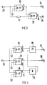
- FIG. 1 An optical transmission system is shown in FIG. 1. It has an optical transmitter 1, a transmission link with an optical waveguide 5 and an optical receiver 2.
- the optical transmitter has a power adder 3, an electrical-optical converter 4, which is preferably a semiconductor laser, two inputs 12, 13 and an output 11. Via the input 13, the power adder 3 receives a first electrical digital signal V 1 and via the input 12 second electrical digital signal V2 supplied. The power adder 3 is connected to the semiconductor laser 4. Its optical signal is coupled into the optical waveguide 5 at the output 11.
- a power adder 3 an electrical-optical converter 4, which is preferably a semiconductor laser, two inputs 12, 13 and an output 11. Via the input 13, the power adder 3 receives a first electrical digital signal V 1 and via the input 12 second electrical digital signal V2 supplied.
- the power adder 3 is connected to the semiconductor laser 4. Its optical signal is coupled into the optical waveguide 5 at the output 11.
- the power adder 3 forms from the digital signals V1, V2 by bitwise addition an electrical multi-stage signal V, the formation of which is explained in more detail in FIG. 2.
- the semiconductor laser is modulated here directly by the electrical multi-stage signal V. It is also possible that instead of the directly modulated laser there is a device in which continuous light emitted by a semiconductor laser is modulated externally by an optical modulator. In this case, the electrical multi-stage signal V is fed to the optical modulator.
- the multistage signal V modulates the frequency or amplitude of the light emitted by the electrical-optical converter 4.
- This multi-stage signal V is particularly advantageous in a transmission system in which signals are transmitted in a frequency-modulated manner.
- Such a system is known from EP-A2-544 736 mentioned above.
- the optical receiver 2 has an optical-electrical converter 6 which e.g. is a PIN photodiode, a decision circuit 7, an optical input 8 and two electrical outputs 9, 10.
- the electrical output of the photodiode 6 is via one or more amplifiers (not shown) with the decision circuit 7 and this with two outputs 9 , 10 connected.
- the optical signal reaching the optical receiver is received at the input 8 by the photodiode 6 and converted into an electrical multistage signal V, which is fed to the decision circuit 7.
- This electrical multi-stage signal V is evaluated by the decision circuit 7.
- the electrical digital signals V1, V2 are shown at the inputs 12, 13 of the optical transmitter 1 and at the outputs 9, 10 of the optical receiver 2.
- the electrical multi-stage signal V is shown at the connection between the power adder 3 and the semiconductor laser 4. For all signals, the course of the amplitude is shown as a function of time.
- a multi-stage signal V which is a four-stage signal here, is shown, which is composed of two electrical digital signals V1, V2. Both Signals have the same bit duration.
- the digital signal V1 has the states "1, 0, 1, 0, 0, 1, 1, 0" and the digital signal V2 has the states "0, 1, 1, 0, 1, 1, 0, 1".
- the amplitude of the digital signal V2 is twice as large as that of the digital signal V1.
- the amplitude as a function of time is also shown.
- That the amplitude of the digital signal V2 is twice as large as that of the digital signal V1, z. B. can be achieved in that the digital signal V1 is attenuated by a factor of 2 with respect to V2. This can be done by an attenuator in or outside the optical transmitter 1. However, this does not matter for the function. It is important that the amplitudes are different.
- the bit duration in the resulting four-stage signal V corresponds to the bit duration of the digital signals V1, V2.
- This four-stage signal thus contains twice the information in one bit duration, namely that of the two digital signals V1, V2. This makes it possible to increase the amount of information to be transmitted by a factor of 2, which corresponds to a doubling of the bit rate.
- decision-making units consist of a comparator and a D flip-flop. Comparators and how they work are well known, e.g. B. from: U. Tietze, C. Schenk: “Semiconductor circuit technology", 8th edition, Springer-Verlag 1986, chapter 8.5.1, page 178. When the input voltage difference passes zero, the output voltage assumes a logic state "1".
- the four-stage signal is fed to the "(+) input” of the comparator and the "(-) input” the corresponding threshold value.
- the output voltage thus assumes a logic state "1", if the four-stage signal V is greater than the respective threshold value.
- the D flip-flop is used to store the respective logic state. The processing of signals takes place synchronously to a uniform clock. To simplify matters, no clock feed is shown in the figures.
- FIG. 3 shows a first exemplary embodiment of a decision-making circuit 7. So that the decision-making circuit 7 present in the optical receiver 2 can recover the two digital signals V 1, V 2 from the four-stage signal V, a threshold value S1 is to be defined. In Fig. 2 this lies in the middle of the four-stage signal V.
- the decision circuit 7 wins back from the four-stage signal V the digital signal V2 according to the proviso that V2 always has the state "1" when the threshold S1 is exceeded.
- the decision circuit 7 has an input 23 for the four-stage signal V, an output 25 for the digital signal V1, an output 24 for the digital signal V2, a first 20 and second decision unit 22 and a delay gate 21st
- Each decision unit 20, 22 has a first output Q and a second output Q ⁇ which is an inverting output.
- the delay gate 21 delays the four-stage signal by the time required for its processing in the first decision unit 20. This is necessary because the difference V-V2 is formed to recover the digital signal V1; V2 must therefore already be recovered at the time the difference is formed.
- the first decision unit 20 compares the four-stage signal V with the threshold value S1. If this is exceeded, the digital signal V2 exits at its first output Q. This corresponds to the output 24 of the decision circuit 7.
- the second decision unit 22 is connected to the first output Q of the decision unit 20 and to the delay gate 21. via which the four-stage signal V is supplied. By the decision unit 22, the already mentioned difference formation V-V2 takes place, so that at its first output Q, which corresponds to the output 25 of the decision circuit 7, the digital signal V1 emerges.
- FIG. 4 A second exemplary embodiment of the decision circuit 7 is shown in FIG. 4. So that the decision circuit 7 present in the optical receiver 2 can recover the two digital signals V 1, V 2 from the four-stage signal V, a first S0, a second S1 and a third threshold value S2 are to be defined. In Fig. 2, the threshold values are set so that they are in the middle between the individual stages.
- the decision circuit 7 has an input 31 for the four-stage signal V, an output 37 for the digital signal V1, an output 38 for the digital signal V2, a first 32, second 33 and third decision unit 34, an "AND" gate 35 and an "OR” gate 36.
- the first decision unit 32 compares the four-stage signal V with the upper threshold value S2.
- the second decision unit 33 compares the four-stage signal V with the middle threshold S1, and the third decision unit 34 compares the four-stage signal V with the lower threshold S0.
- the digital signal V2 exits.
- the second exit Q ⁇ the second decision unit 33 and the first output Q of the third decision unit 34 are connected to the "AND" gate 35, the output of which is connected to the "OR” gate 36.
- the "OR” gate 36 is also connected to the first output Q of the first decision unit 32, so that the digital signal V 1 exits at the output of the "OR" gate 36. This output corresponds to the output 37 of the decision circuit 7 and that at which the digital signal V2 emerges corresponds to the output 38.
Abstract
Description
Die Erfindung betrifft ein optisches Übertragungssystem nach dem Oberbegriff des Anspruchs 1. Außerdem betrifft die Erfindung einen optischen Sender mit einem elektrisch-optisch Wandler nach dem Oberbegriff des Anspruchs 2. Schließlich betrifft die Erfindung eine Entscheider-Schaltung zur Verwendung in dem erfindungsgemäßen Übertragungssystem. Sie ist Gegenstand der Ansprüche 4 bis 6.The invention relates to an optical transmission system according to the preamble of
Optische Übertragungssysteme mit den im Oberbegriff des Anspruchs 1 angeführten Merkmalen und die darin eingesetzten optischen Sender sind hinreichend bekannt, z. B. aus: EP-A2-554 736. Dort ist auf der Sendeseite ein elektrisch-optisch Wandler gezeigt, der ein von einem elektrischen Digitalsignal frequenzmoduliertes optisches Signal aussendet. Die Übertragung erfolgt über einen Lichtwellenleiter zu einem optischen Empfänger, der einen optisch-elektrisch Wandler und einen Entscheider hat. Mit dem Entscheider wird das Digitalsignal zurückgewonnen.Optical transmission systems with the features listed in the preamble of
Bei der optischen Übertragung von Digitalsignalen besteht der Wunsch, die Übertragungsgeschwindigkeit dieser Signale zu erhöhen, d.h. die Bitfolgefrequenz beispielsweise auf 40 Gbit/s zu erhöhen.In the optical transmission of digital signals, there is a desire to increase the transmission speed of these signals, ie to increase the bit rate, for example to 40 Gbit / s.
Aus der Literatur sind Systeme bekannt, in denen Signale mit einer Bitfolgefrequenz von 10 Gbit/s übertragbar sind. Aus B. Wedding et al, "10 Gbit/s To 260 000 Subscribers Using Optical Amplifier Distribution Network", Contribution für ICC/Supercom '92, Optical Communications 300 Level Session "Impact of Optical Amplifiers on Network Architectures" ist beispielsweise bekannt, für diese Bitfolgefrequenz einen Laser (high-speed multiquantum well DFB-Laser, MQW DFB-Laser) direkt zu modulieren. Direkte Modulation bedeutet, daß der Injektionsstrom des Lasers in Abhängigkeit des zu übertragenden Signals variiert wird. Dadurch ist eine Intensitätsoder Frequenzmodulation möglich. Für diese Anwendung, 10 Gbit/s-Übertragung, muß der DFB-Laser optimiert werden, um unerwünschte Modulationseigenschaften zu reduzieren. Zu diesen unerwünschten Eigenschaften gehören z.B. der Chirp-Effekt und parasitäre Impedanzen der Laser. Unter dem Chirp-Effekt versteht man eine Frequenzinstabilität, die bei der Modulation auftritt.Systems are known from the literature in which signals with a bit repetition frequency of 10 Gbit / s can be transmitted. For example, from B. Wedding et al, "10 Gbit / s To 260,000 Subscribers Using Optical Amplifier Distribution Network", Contribution for ICC / Supercom '92, Optical Communications 300 Level Session "Impact of Optical Amplifiers on Network Architectures" to modulate this bit rate directly with a laser (high-speed multiquantum well DFB laser, MQW DFB laser). Direct modulation means that the injection current of the laser is varied depending on the signal to be transmitted. This enables intensity or frequency modulation. For this application, 10 Gbit / s transmission, the DFB laser must be optimized to reduce undesirable modulation properties. These undesirable properties include e.g. the chirp effect and parasitic impedances of the lasers. The chirp effect is a frequency instability that occurs during modulation.
Aus diesen Gründen ist eine obere Grenze der Bitfolgefrequenz erkennbar, oberhalb derer direkt modulierte Laser, wie sie bisher zum Einsatz kommen, nicht mehr verwendet werden können. Auch für die Ansteuerelektronik des Lasers besteht eine obere Grenze.For these reasons, an upper limit of the bit repetition frequency can be seen, above which directly modulated lasers, as have been used up to now, can no longer be used. There is also an upper limit for the control electronics of the laser.
Der Erfindung liegt die Aufgabe zugrunde, ein optisches Übertragungssystem anzugeben, in dem Signale mit einer hohen Bitfolgefrequenz übertragen werden können. Diese Aufgabe ist wie in Anspruch 1 angegeben gelöst.The invention has for its object to provide an optical transmission system in which signals can be transmitted with a high bit rate. This object is achieved as indicated in
Außerdem liegt der Erfindung die Aufgabe zugrunde, einen optischen Sender für ein solches System anzugeben. Diese Aufgabe ist wie in Anspruch 2 angegeben gelöst. Weiterbildungen der Erfindung sind in den Unteransprüchen angegeben.The invention is also based on the object of specifying an optical transmitter for such a system. This object is achieved as indicated in
Ein Vorteil der Erfindung ist, daß die Erhöhung der Bitfolgefrequenz in diesem optischen Übertragungssystem mit unveränderten Lasern und einer unveränderten Ansteuerelektronik möglich ist.An advantage of the invention is that the bit repetition frequency can be increased in this optical transmission system with unchanged lasers and unchanged control electronics.
Die Erfindung wird nun anhand der Figuren durch Beispiele näher erläutert. Es zeigen:
- Fig. 1
- ein erfindungsgemäßes optisches Übertragungssystem mit einem optischen Sender,
- Fig. 2
- ein Beispiel zur Bildung eines Mehrstufensignals,
- Fig. 3
- ein erstes Ausführungsbeispiel einer Entscheider-Schaltung,
- Fig. 4
- ein zweites Ausführungsbeispiel einer Entscheider-Schaltung.
- Fig. 1
- an optical transmission system according to the invention with an optical transmitter,
- Fig. 2
- an example of the formation of a multi-stage signal,
- Fig. 3
- a first embodiment of a decision circuit,
- Fig. 4
- a second embodiment of a decision circuit.
Ein optisches Übertragungssystem ist in Fig. 1 gezeigt. Es hat einen optischen Sender 1, eine Übertragungsstrecke mit einem Lichtwellenleiter 5 und einen optischen Empfänger 2.An optical transmission system is shown in FIG. 1. It has an
Der optische Sender hat einen Leistungsaddierer 3, einen elektrisch-optisch Wandler 4, der vorzugsweise ein Halbleiterlaser ist, zwei Eingänge 12, 13 und einen Ausgang 11. Über den Eingang 13 wird dem Leistungsaddierer 3 ein erstes elektrisches Digitalsignal V₁ und über den Eingang 12 ein zweites elektrisches Digitalsignal V₂ zugeführt. Der Leistungsaddierer 3 ist mit dem Halbleiterlaser 4 verbunden. Dessen optisches Signal wird an dem Ausgang 11 in den Lichtwellenleiter 5 eingekoppelt.The optical transmitter has a power adder 3, an electrical-optical converter 4, which is preferably a semiconductor laser, two inputs 12, 13 and an output 11. Via the input 13, the power adder 3 receives a first electrical
Der Leistungsaddierer 3 bildet aus den Digitalsignalen V₁, V₂ durch bitweise Addition ein elektrisches Mehrstufensignal V, dessen Bildung in Fig. 2 noch genauer erläutert wird.The power adder 3 forms from the digital signals V₁, V₂ by bitwise addition an electrical multi-stage signal V, the formation of which is explained in more detail in FIG. 2.
Der Halbleiterlaser wird hier durch das elektrische Mehrstufensignal V direkt moduliert. Es ist auch möglich, daß anstatt des direkt modulierten Lasers eine Einrichtung vorhanden ist, in der von einem Halbleiterlaser emittiertes kontinuierliches Licht extern durch einen optischen Modulator moduliert wird. Das elektrische Mehrstufensignal V wird in diesem Fall dem optischen Modulator zugeführt.The semiconductor laser is modulated here directly by the electrical multi-stage signal V. It is also possible that instead of the directly modulated laser there is a device in which continuous light emitted by a semiconductor laser is modulated externally by an optical modulator. In this case, the electrical multi-stage signal V is fed to the optical modulator.
Das Mehrstufensignal V moduliert das vom elektrisch-optisch Wandler 4 emittierte Licht in seiner Frequenz oder Amplitude. Besonders vorteilhaft ist dieses Mehrstufensignal V in einem Übertragungssystem, in dem Signale frequenzmoduliert übertragen werden. Ein solches System ist aus der oben erwähnten EP-A2-544 736 bekannt.The multistage signal V modulates the frequency or amplitude of the light emitted by the electrical-optical converter 4. This multi-stage signal V is particularly advantageous in a transmission system in which signals are transmitted in a frequency-modulated manner. Such a system is known from EP-A2-544 736 mentioned above.
Der optische Empfänger 2 hat einen optisch-elektrisch Wandler 6, der z.B. eine PIN-Photodiode ist, eine Entscheider-Schaltung 7, einen optischen Eingang 8 und zwei elektrische Ausgänge 9, 10. Der elektrische Ausgang der Photodiode 6 ist über einen oder mehrere nicht gezeigte Verstärker mit der Entscheider-Schaltung 7 und diese mit zwei Ausgängen 9, 10 verbunden. Das zum optischen Empfänger gelangende optische Signal wird an dem Eingang 8 von der Photodiode 6 empfangen und in ein elektrisches Mehrstufensignal V gewandelt, das der Entscheider-Schaltung 7 zugeführt wird. Dieses elektrische Mehrstufensignal V wird durch die Entscheider-Schaltung 7 ausgewertet. Die elektrischen Digitalsignale V₁, V₂ sind an den Eingängen 12, 13 des optischen Senders 1 und an den Ausgängen 9, 10 des optischen Empfängers 2 dargestellt. Das elektrische Mehrstufensignal V ist an der Verbindung zwischen Leistungsaddierer 3 und Halbleiterlaser 4 gezeigt. Bei allen Signalen ist der Verlauf der Amplitude als Funktion der Zeit dargestellt.The
In Fig. 2 ist ein Beispiel zur Bildung eines Mehrstufensignals V, das hier ein Vierstufensignal ist, gezeigt, das aus zwei elektrischen Digitalsignalen V₁, V₂ zusammengesetzt ist. Beide Signale haben die gleiche Bitdauer. Das Digitalsignal V₁ hat die Zustände "1, 0, 1, 0, 0, 1, 1, 0" und das Digitalsignal V₂ die Zustände "0, 1, 1, 0, 1, 1, 0, 1". Die Amplitude des Digitalsignals V₂ ist doppelt so groß wie die des Digitalsignals V₁. Es ist ebenfalls die Amplitude als Funktion der Zeit dargestellt.In Fig. 2 an example of the formation of a multi-stage signal V, which is a four-stage signal here, is shown, which is composed of two electrical digital signals V₁, V₂. Both Signals have the same bit duration. The digital signal V₁ has the states "1, 0, 1, 0, 0, 1, 1, 0" and the digital signal V₂ has the states "0, 1, 1, 0, 1, 1, 0, 1". The amplitude of the digital signal V₂ is twice as large as that of the digital signal V₁. The amplitude as a function of time is also shown.
Durch bitweise Addition der beiden Digitalsignale V₁, V₂ ergibt sich das Vierstufensignal V, d.h. ![]()
![]()
Daß die Amplitude des Digitalsignals V₂ doppelt so groß wie die des Digitalsignals V₁ ist, kann z. B. dadurch erreicht werden, daß das Digitalsignal V₁ bezüglich V₂ um den Faktor 2 gedämpft wird. Dies kann durch ein Dämpfungsglied im oder außerhalb des optischen Senders 1 erfolgen. Für die Funktion spielt dies jedoch keine Rolle. Wichtig ist, daß die Amplituden unterschiedlich sind.That the amplitude of the digital signal V₂ is twice as large as that of the digital signal V₁, z. B. can be achieved in that the digital signal V₁ is attenuated by a factor of 2 with respect to V₂. This can be done by an attenuator in or outside the
Die Bitdauer in dem entstandenen Vierstufensignal V entspricht der Bitdauer der Digitalsignale V₁, V₂. In diesem Vierstufensignal steckt somit in einer Bitdauer die doppelte Information, nämlich die der beiden Digitalsignale V₁, V₂. Dadurch ist es möglich, die zu übertragende Informationsmenge um einen Faktor 2 zu erhöhen, was einer Verdoppelung der Bitfolgefrequenz entspricht.The bit duration in the resulting four-stage signal V corresponds to the bit duration of the digital signals V₁, V₂. This four-stage signal thus contains twice the information in one bit duration, namely that of the two digital signals V₁, V₂. This makes it possible to increase the amount of information to be transmitted by a factor of 2, which corresponds to a doubling of the bit rate.
In den folgenden Figuren werden Entscheider-Einheiten verwendet, die aus der Reihenschaltung eines Komparators und eines D-Flip-Flop bestehen. Komparatoren und deren Funktionsweise sind hinreichend bekannt, z. B. aus: U. Tietze, C. Schenk: "Halbleiter-Schaltungstechnik", 8. Auflage, Springer-Verlag 1986, Kapitel 8.5.1, Seite 178. Beim Nulldurchgang der Eingangsspannungsdifferenz nimmt die Ausgangsspannung einen logischen Zustand "1" ein.In the following figures, decision-making units are used which consist of a comparator and a D flip-flop. Comparators and how they work are well known, e.g. B. from: U. Tietze, C. Schenk: "Semiconductor circuit technology", 8th edition, Springer-Verlag 1986, chapter 8.5.1, page 178. When the input voltage difference passes zero, the output voltage assumes a logic state "1".
In der Anwendung entsprechend der folgenden Figuren wird das Vierstufensignal dem "(+)-Eingang" des Komparators zugeführt und dem "(-)-Eingang" der entsprechende Schwellenwert. Die Ausgangsspannung nimmt hier somit einen logischen Zustand "1" ein, wenn das Vierstufensignal V größer als der jeweilige Schwellenwert ist. Das D-Flip-Flop dient zur Speicherung des jeweiligen logischen Zustands. Die Verarbeitung von Signalen erfolgt synchron zu einem einheitlichen Takt. In den Figuren ist zur Vereinfachung keine Taktzuführung gezeigt.In the application according to the following figures, the four-stage signal is fed to the "(+) input" of the comparator and the "(-) input" the corresponding threshold value. The output voltage thus assumes a logic state "1", if the four-stage signal V is greater than the respective threshold value. The D flip-flop is used to store the respective logic state. The processing of signals takes place synchronously to a uniform clock. To simplify matters, no clock feed is shown in the figures.
In Fig. 3 ist ein erstes Ausführungsbeispiel einer Entscheider-Schaltung 7 gezeigt. Damit die im optischen Empfänger 2 vorhandene Entscheider-Schaltung 7 aus dem Vierstufensignal V die beiden Digitalsignale V₁, V₂ zurückgewinnen kann, ist ein Schwellenwert S1 festzulegen. In Fig. 2 liegt dieser in der Mitte des Vierstufensignals V. Die Entscheider-Schaltung 7 gewinnt aus dem Vierstufensignal V das Digitalsignal V₂ nach der Maßgabe zurück, daß V₂ immer dann den Zustand "1" hat, wenn der Schwellenwert S1 überschritten ist. Das Digitalsignal V₁ gewinnt sie entsprechend der Gleichung ![]()
![]()
Die Entscheider-Schaltung 7 hat einen Eingang 23 für das Vierstufensignal V, einen Ausgang 25 für das Digitalsignal V₁, einen Ausgang 24 für das Digitalsignal V₂, eine erste 20 und zweite Entscheider-Einheit 22 und ein Verzögerungsgatter 21.The decision circuit 7 has an
Jede Entscheider-Einheit 20, 22 hat einen ersten Ausgang Q und einen zweiten Ausgang ![]()
Die erste Entscheider-Einheit 20 vergleicht das Vierstufensignal V mit dem Schwellenwert S1. Ist dieser überschritten, tritt an deren erstem Ausgang Q das Digitalsignal V₂ aus. Dieser entspricht dem Ausgang 24 der Entscheider-Schaltung 7. Die zweite Entscheider-Einheit 22 ist mit dem ersten Ausgang Q der Entscheider-Einheit 20 und mit dem Verzögerungsgatter 21 verbunden, über das das Vierstufensignal V zugeführt wird. Durch die Entscheider-Einheit 22 erfolgt die bereits erwähnte Differenzbildung V-V₂, so daß an deren erstem Ausgang Q, der dem Ausgang 25 der Entscheider-Schaltung 7 entspricht, das Digitalsignal V₁ austritt.Each ![]()
The
Ein zweites Ausführungsbeispiel der Entscheider-Schaltung 7 ist in Fig. 4 gezeigt. Damit die im optischen Empfänger 2 vorhandene Entscheider-Schaltung 7 aus dem Vierstufensignal V die beiden Digitalsignale V₁, V₂ zurückgewinnen kann, sind ein erster S0, ein zweiter S1 und ein dritter Schwellenwert S2 festzulegen. In Fig. 2 sind die Schwellenwerte so festgelegt, daß diese jeweils in der Mitte zwischen den einzelnen Stufen liegen.A second exemplary embodiment of the decision circuit 7 is shown in FIG. 4. So that the decision circuit 7 present in the
Sie gewinnt aus dem Vierstufensignal V das Digitalsignal V₂, ebenso wie in Fig. 3, nach der Maßgabe zurück, daß V₂ immer dann den Zustand "1" hat, wenn der Schwellenwert S1 überschritten ist. Das Digitalsignal V₁ gewinnt sie hier dadurch zurück, daß V₁ immer dann den Zustand "1" hat, wenn der Schwellenwert S2 überschritten ist oder wenn der Schwellenwert S0 überschritten ist und der Schwellenwert S1 nicht überschritten ist.You wins from the four-stage signal V, the digital signal V₂, as in Fig. 3, on the proviso that V₂ always has the state "1" when the threshold S1 is exceeded. The
Die Entscheider-Schaltung 7 hat einen Eingang 31 für das Vierstufensignal V einen Ausgang 37 für das Digitalsignal V₁, einen Ausgang 38 für das Digitalsignal V₂, eine erste 32, zweite 33 und dritte Entscheider-Einheit 34, ein "UND"-Gatter 35 und ein "ODER"-Gatter 36.
Die erste Entscheider-Einheit 32 vergleicht das Vierstufensignal V mit dem oberen Schwellenwert S2. Die zweite Entscheider-Einheit 33 vergleicht das Vierstufensignal V mit dem mittleren Schwellenwert S1, und die dritte Entscheider-Einheit 34 vergleicht das Vierstufensignal V mit dem unteren Schwellenwert S0.The decision circuit 7 has an input 31 for the four-stage signal V, an
The
Am ersten Ausgang Q der zweiten Entscheider-Einheit 33 tritt das Digitalsignal V₂ aus. Der zweite Ausgang ![]()
![]()
Das "ODER"-Gatter 36 ist außerdem mit dem ersten Ausgang Q der ersten Entscheider-Einheit 32 verbunden, so daß am Ausgang des "ODER"-Gatters 36 das Digitalsignal V₁ austritt. Dieser Ausgang entspricht dem Ausgang 37 der Entscheider-Schaltung 7 und der, an dem das Digitalsignal V₂ austritt, entspricht dem Ausgang 38.The "OR"
In diesem Übertragungssystem können auch mehr als zwei elektrische Digitalsignale durch den Leistungsaddierer (3) addiert werden. In diesem Fall kann die Bitfolgefrequenz nochmals erhöht werden.In this transmission system, more than two electrical digital signals can also be added by the power adder (3). In this case, the bit rate can be increased again.
Claims (8)
dadurch gekennzeichnet, daß der optische Sender (1) einen elektrischen Leistungsaddierer (3) hat, der ein erstes (V₁) und ein zweites ihm zugeführtes elektrisches Digitalsignal (V₂) gleicher Bitdauer und unterschiedlicher Amplitude bitweise addiert, so daß daraus ein elektrisches Mehrstufensignal (V) entsteht, das der elektrisch-optisch Wandler (4) in ein optisches Signal wandelt und über den Lichtwellenleiter (5) zum optischen Empfänger (2) sendet, in dem die Entscheider-Schaltung (7) aus dem durch den optisch-elektrisch Wandler (6) entstandenen elektrischen Mehrstufensignal (V) die Digitalsignale (V₁, V₂) zurückgewinnt.Optical transmission system with an optical transmitter (1), which has an electrical-optical converter (4), an optical waveguide (5) and an optical receiver (2), which has an optical-electrical converter (6) and a decision circuit (7 ) Has,
characterized in that the optical transmitter (1) has an electrical power adder (3) which adds a first (V₁) and a second supplied electrical digital signal (V₂) of the same bit duration and different amplitude bit by bit, so that an electrical multi-stage signal (V ) arises, which the electrical-optical converter (4) converts into an optical signal and sends via the optical fiber (5) to the optical receiver (2), in which the decision-making circuit (7) consists of the optical-electrical converter 6) generated electrical multi-stage signal (V), the digital signals (V₁, V₂) recovered.
dadurch gekennzeichnet, daß er einen Leistungsaddierer (3) hat, der ein erstes (V₁) und ein zweites ihm zugeführtes elektrisches Digitalsignal (V₂) gleicher Bitdauer und unterschiedlicher Amplitude bitweise addiert, so daß daraus ein elektrisches Mehrstufensignal (V) entsteht, das der elektrisch-optisch Wandler (4) in ein optisches Signal wandelt und aussendet.Optical transmitter (1) with an electrical-optical converter (4)
characterized in that it has a power adder (3) which adds a first (V₁) and a second supplied to it electrical digital signal (V₂) of the same bit duration and different amplitude bit by bit, so that an electrical multi-stage signal (V) arises from this, which the electrical -optically converts (4) into an optical signal and sends it out.
dadurch gekennzeichnet, daß das Mehrstufensignal (V) ein Vierstufensignal ist, das aus zwei Digitalsignalen (V₁, V₂) zusammengesetzt ist.Optical transmission system according to claim 1,
characterized in that the multi-stage signal (V) is a four-stage signal which is composed of two digital signals (V₁, V₂).
dadurch gekennzeichnet, daß in der Entscheider-Schaltung (7) ein unterer (S0), ein mittlerer (S1) und ein oberer Schwellenwert (S2) festgelegt sind, daß sie einen Zustand "1" des zweiten Digitalsignals (V₂) detektiert, wenn der mittlere Schwellenwert (S1) überschritten ist und sie einen Zustand "1" des ersten Digitalsignals (V₁) detektiert, wenn der obere Schwellenwert (S2) überschritten ist oder wenn der untere Schwellenwert (S0) überschritten ist und der erste Schwellenwert (S1) nicht überschritten ist.Optical transmission system according to claim 3 or the decision circuit for such a transmission system
characterized in that a lower (S0), a middle (S1) and an upper threshold value (S2) are defined in the decision circuit (7) in that it detects a state "1" of the second digital signal (V₂) when the average threshold (S1) is exceeded and it detects a state "1" of the first digital signal (V₁) when the upper threshold (S2) is exceeded or when the lower threshold (S0) is exceeded and the first threshold (S1) is not exceeded is.
dadurch gekennzeichnet, daß die Entscheider-Schaltung (7) eine erste (32), eine zweite (33) und eine dritte Entscheider-Einheit (34), die jeweils einen ersten (Q) und einen zweiten Ausgang (
characterized in that the decision circuit (7) has a first (32), a second (33) and a third decision unit (34), each having a first (Q) and a second output (
Applications Claiming Priority (2)
| Application Number | Priority Date | Filing Date | Title |
|---|---|---|---|
| DE4341408 | 1993-12-04 | ||
| DE4341408A DE4341408A1 (en) | 1993-12-04 | 1993-12-04 | Optical system for the transmission of a multi-stage signal |
Publications (1)
| Publication Number | Publication Date |
|---|---|
| EP0656700A1 true EP0656700A1 (en) | 1995-06-07 |
Family
ID=6504208
Family Applications (1)
| Application Number | Title | Priority Date | Filing Date |
|---|---|---|---|
| EP94118819A Ceased EP0656700A1 (en) | 1993-12-04 | 1994-11-30 | Optical system for transmitting a multilevel signal |
Country Status (4)
| Country | Link |
|---|---|
| US (1) | US5510919A (en) |
| EP (1) | EP0656700A1 (en) |
| AU (1) | AU683942B2 (en) |
| DE (1) | DE4341408A1 (en) |
Cited By (2)
| Publication number | Priority date | Publication date | Assignee | Title |
|---|---|---|---|---|
| WO2002067521A1 (en) | 2001-03-29 | 2002-08-29 | Quellan, Inc. | Increasing data throughput in optical fiber transmission systems |
| US7466765B2 (en) | 2001-09-10 | 2008-12-16 | Alcatel | Receiver for high bitrate binary signals |
Families Citing this family (56)
| Publication number | Priority date | Publication date | Assignee | Title |
|---|---|---|---|---|
| JP2609831B2 (en) * | 1995-03-15 | 1997-05-14 | エヌイーシーテレネットワークス株式会社 | Optical duplex transmission method |
| US5657153A (en) * | 1995-03-21 | 1997-08-12 | Sdl, Inc. | Optical amplifier with complementary modulation signal inputs |
| DE19737482A1 (en) | 1997-08-28 | 1999-03-04 | Alsthom Cge Alcatel | Process for optical transmission over an optical fiber network, and optical transmission network |
| EP0923204B1 (en) | 1997-12-11 | 2005-02-23 | Alcatel | Optical receiver for receiving digital transmitted data |
| DE19815011A1 (en) * | 1998-04-03 | 1999-10-14 | Temic Semiconductor Gmbh | Process for the transmission of digital transmission signals |
| GB9825046D0 (en) * | 1998-11-17 | 1999-01-13 | Barr & Stroud Ltd | Data communications link |
| US6265971B1 (en) | 1999-04-09 | 2001-07-24 | Simplex Time Recorder Company | Fiber-sync communications channel |
| KR100303315B1 (en) | 1999-08-05 | 2001-11-01 | 윤종용 | Optical receivers with bit-rate independent clock and data recovery and method thereof |
| GB2366106B (en) * | 2000-08-19 | 2004-06-23 | Marconi Caswell Ltd | Multi-level optical signal generation |
| GB2366677B (en) | 2000-09-09 | 2004-05-19 | Ibm | Optical amplitude modulator |
| AU2002210878A1 (en) * | 2000-10-10 | 2002-04-22 | Trellis Photonics Ltd. | Method, device, and system, for multiple order amplitude modulation of an optical signal, and demodulation thereof |
| US7173551B2 (en) * | 2000-12-21 | 2007-02-06 | Quellan, Inc. | Increasing data throughput in optical fiber transmission systems |
| US6490069B1 (en) | 2001-01-29 | 2002-12-03 | Stratalight Communications, Inc. | Transmission and reception of duobinary multilevel pulse-amplitude-modulated optical signals using subtraction-based encoder |
| US6445476B1 (en) | 2001-01-29 | 2002-09-03 | Stratalight Communications, Inc. | Transmission and reception of duobinary multilevel pulse-amplitude-modulated optical signals using subsequence-based encoder |
| US6424444B1 (en) | 2001-01-29 | 2002-07-23 | Stratalight Communications, Inc. | Transmission and reception of duobinary multilevel pulse-amplitude-modulated optical signals using finite-state machine-based encoder |
| US7307569B2 (en) * | 2001-03-29 | 2007-12-11 | Quellan, Inc. | Increasing data throughput in optical fiber transmission systems |
| US7149256B2 (en) | 2001-03-29 | 2006-12-12 | Quellan, Inc. | Multilevel pulse position modulation for efficient fiber optic communication |
| US6643471B2 (en) | 2001-04-02 | 2003-11-04 | Adc Telecommunications, Inc. | Increased transmission capacity for a fiber-optic link |
| DE60238602D1 (en) * | 2001-04-04 | 2011-01-27 | Quellan Inc | METHOD AND SYSTEM FOR DECODING MULTI-LEVEL SIGNALS |
| JP4704596B2 (en) * | 2001-04-26 | 2011-06-15 | 三菱電機株式会社 | Optical quaternary modulator and optical quaternary modulation method |
| JP4744720B2 (en) * | 2001-05-08 | 2011-08-10 | 三菱電機株式会社 | Multilevel modulator |
| US20030030873A1 (en) * | 2001-05-09 | 2003-02-13 | Quellan, Inc. | High-speed adjustable multilevel light modulation |
| US6690894B2 (en) | 2001-05-14 | 2004-02-10 | Stratalight Communications, Inc. | Multilevel optical signals optimized for systems having signal-dependent and signal-independent noises, finite transmitter extinction ratio and intersymbol interference |
| AU2003211094A1 (en) * | 2002-02-15 | 2003-09-09 | Quellan, Inc. | Multi-level signal clock recovery technique |
| JP3788945B2 (en) * | 2002-02-28 | 2006-06-21 | 株式会社東芝 | Multiplexed optical transmission equipment |
| US6816101B2 (en) * | 2002-03-08 | 2004-11-09 | Quelian, Inc. | High-speed analog-to-digital converter using a unique gray code |
| WO2003092237A1 (en) * | 2002-04-23 | 2003-11-06 | Quellan, Inc. | Combined ask/dpsk modulation system |
| JP2004013681A (en) * | 2002-06-10 | 2004-01-15 | Bosu & K Consulting Kk | Name card information managing system |
| US7023888B2 (en) * | 2002-06-13 | 2006-04-04 | Agilent Technologies, Inc. | Multilevel optical signal generator and method thereof |
| JP4145583B2 (en) * | 2002-07-02 | 2008-09-03 | シャープ株式会社 | Signal transmission method, signal transmission system, logic circuit, and liquid crystal driving device |
| AU2003256569A1 (en) * | 2002-07-15 | 2004-02-02 | Quellan, Inc. | Adaptive noise filtering and equalization |
| US7934144B2 (en) | 2002-11-12 | 2011-04-26 | Quellan, Inc. | High-speed analog-to-digital conversion with improved robustness to timing uncertainty |
| EP1420532A1 (en) * | 2002-11-15 | 2004-05-19 | Alcatel | System for multiplexing and transmission of asynchronous data signals |
| GB2421674B (en) * | 2003-08-07 | 2006-11-15 | Quellan Inc | Method and system for crosstalk cancellation |
| US7804760B2 (en) * | 2003-08-07 | 2010-09-28 | Quellan, Inc. | Method and system for signal emulation |
| US7123676B2 (en) * | 2003-11-17 | 2006-10-17 | Quellan, Inc. | Method and system for antenna interference cancellation |
| US7616700B2 (en) * | 2003-12-22 | 2009-11-10 | Quellan, Inc. | Method and system for slicing a communication signal |
| US7725079B2 (en) * | 2004-12-14 | 2010-05-25 | Quellan, Inc. | Method and system for automatic control in an interference cancellation device |
| US7522883B2 (en) | 2004-12-14 | 2009-04-21 | Quellan, Inc. | Method and system for reducing signal interference |
| DE112007001045B4 (en) * | 2006-04-26 | 2019-05-16 | Intersil Americas LLC | Method and system for reducing radiation emissions from a communication channel |
| US8483570B2 (en) * | 2007-05-28 | 2013-07-09 | Multipon Networks Ltd. | Method and apparatus for increasing the capacity of a data communication channel |
| KR101430168B1 (en) * | 2008-01-09 | 2014-08-13 | 삼성전자주식회사 | Optical interconnection system transmitting and receiving 3-level signal |
| DE602008003000D1 (en) * | 2008-04-03 | 2010-11-25 | Alcatel Lucent | Data recovery for a multi-speed, multi-level signal |
| JP5583999B2 (en) * | 2010-03-24 | 2014-09-03 | 太陽誘電株式会社 | Visible light communication transmitter and visible light communication system |
| EP2618531B1 (en) * | 2012-01-20 | 2014-12-24 | ADVA Optical Networking SE | Method and device for transmitting a low-frequency signal over a data transmission link using a digital high bit-rate signal |
| JP6998691B2 (en) * | 2017-07-19 | 2022-01-18 | 日本ルメンタム株式会社 | Optical transmission module |
| JP6988604B2 (en) * | 2018-03-16 | 2022-01-05 | 日本電信電話株式会社 | Optical modulation / demodulation method, optical communication system, optical transmitter and receiver |
| US10897315B2 (en) * | 2019-04-18 | 2021-01-19 | Microsoft Technology Licensing, Llc | Power-based decoding of data received over an optical communication path |
| US11018776B2 (en) | 2019-04-18 | 2021-05-25 | Microsoft Technology Licensing, Llc | Power-based decoding of data received over an optical communication path |
| US10911152B2 (en) * | 2019-04-18 | 2021-02-02 | Microsoft Technology Licensing, Llc | Power-based decoding of data received over an optical communication path |
| US10911155B2 (en) | 2019-04-18 | 2021-02-02 | Microsoft Technology Licensing, Llc | System for throughput increases for optical communications |
| US10938485B2 (en) | 2019-04-18 | 2021-03-02 | Microsoft Technology Licensing, Llc | Error control coding with dynamic ranges |
| US10873393B2 (en) | 2019-04-18 | 2020-12-22 | Microsoft Technology Licensing, Llc | Receiver training for throughput increases in optical communications |
| US10951342B2 (en) | 2019-04-18 | 2021-03-16 | Microsoft Technology Licensing, Llc | Throughput increases for optical communications |
| US10862591B1 (en) | 2019-04-18 | 2020-12-08 | Microsoft Technology Licensing, Llc | Unequal decision regions for throughput increases for optical communications |
| US10998982B2 (en) | 2019-04-18 | 2021-05-04 | Microsoft Technology Licensing, Llc | Transmitter for throughput increases for optical communications |
Citations (3)
| Publication number | Priority date | Publication date | Assignee | Title |
|---|---|---|---|---|
| DE3525105A1 (en) * | 1985-07-13 | 1987-01-15 | Telefonbau & Normalzeit Gmbh | Method and circuit arrangement for transmitting information via a transmission path |
| DE4035996A1 (en) * | 1990-11-12 | 1992-05-14 | Siemens Ag | METHOD FOR THE SIMULTANEOUS TRANSMISSION OF DATA ON A TRANSMISSION CHANNEL |
| EP0554736A2 (en) * | 1992-02-01 | 1993-08-11 | Alcatel SEL Aktiengesellschaft | Digital optical transmission system with a dispersing optical waveguide at the working wavelength |
Family Cites Families (10)
| Publication number | Priority date | Publication date | Assignee | Title |
|---|---|---|---|---|
| US3571725A (en) * | 1967-05-25 | 1971-03-23 | Nippon Electric Co | Multilevel signal transmission system |
| JPS6030456B2 (en) * | 1978-02-23 | 1985-07-16 | 富士通株式会社 | Optical bipolar communication system |
| DE2944459C2 (en) * | 1979-11-03 | 1984-04-26 | ANT Nachrichtentechnik GmbH, 7150 Backnang | Method for transmitting bipolar signals by means of an optical transmitter |
| US4524462A (en) * | 1982-06-24 | 1985-06-18 | Italtel Societa Italiana Telecomunicazioni S.P.A. | System for jointly transmitting high-frequency and low-frequency digital signals over a fiber-optical carrier |
| DE3523467A1 (en) * | 1985-07-01 | 1987-01-08 | Hirschmann Radiotechnik | Method for digital transmission of analogue signals |
| DE3544393A1 (en) * | 1985-12-16 | 1987-06-19 | Philips Patentverwaltung | SERVICE-INTEGRATING, DIGITAL MESSAGE TRANSMISSION SYSTEM WITH DEVICES FOR THE COMMON TRANSMISSION OF NARROWBAND AND BROADBAND SIGNALS |
| DE8716160U1 (en) * | 1987-12-07 | 1988-01-28 | Fa. Andreas Hettich, 7200 Tuttlingen, De | |
| JPH01223837A (en) * | 1988-03-03 | 1989-09-06 | Nec Corp | Optical multi-value transmitter |
| JPH03291036A (en) * | 1990-04-06 | 1991-12-20 | Fujitsu Ltd | Common reception and decoding circuit for zero return signal and non-zero return signal |
| JP2707891B2 (en) * | 1991-10-18 | 1998-02-04 | 日本電気株式会社 | Optical receiving circuit |
-
1993
- 1993-12-04 DE DE4341408A patent/DE4341408A1/en not_active Withdrawn
-
1994
- 1994-11-28 AU AU79045/94A patent/AU683942B2/en not_active Ceased
- 1994-11-28 US US08/345,618 patent/US5510919A/en not_active Expired - Fee Related
- 1994-11-30 EP EP94118819A patent/EP0656700A1/en not_active Ceased
Patent Citations (3)
| Publication number | Priority date | Publication date | Assignee | Title |
|---|---|---|---|---|
| DE3525105A1 (en) * | 1985-07-13 | 1987-01-15 | Telefonbau & Normalzeit Gmbh | Method and circuit arrangement for transmitting information via a transmission path |
| DE4035996A1 (en) * | 1990-11-12 | 1992-05-14 | Siemens Ag | METHOD FOR THE SIMULTANEOUS TRANSMISSION OF DATA ON A TRANSMISSION CHANNEL |
| EP0554736A2 (en) * | 1992-02-01 | 1993-08-11 | Alcatel SEL Aktiengesellschaft | Digital optical transmission system with a dispersing optical waveguide at the working wavelength |
Cited By (4)
| Publication number | Priority date | Publication date | Assignee | Title |
|---|---|---|---|---|
| WO2002067521A1 (en) | 2001-03-29 | 2002-08-29 | Quellan, Inc. | Increasing data throughput in optical fiber transmission systems |
| EP1374515A1 (en) * | 2001-03-29 | 2004-01-02 | Quellan, Inc. | Increasing data throughput in optical fiber transmission systems |
| EP1374515A4 (en) * | 2001-03-29 | 2009-12-02 | Quellan Inc | Increasing data throughput in optical fiber transmission systems |
| US7466765B2 (en) | 2001-09-10 | 2008-12-16 | Alcatel | Receiver for high bitrate binary signals |
Also Published As
| Publication number | Publication date |
|---|---|
| AU7904594A (en) | 1995-06-15 |
| AU683942B2 (en) | 1997-11-27 |
| US5510919A (en) | 1996-04-23 |
| DE4341408A1 (en) | 1995-06-08 |
Similar Documents
| Publication | Publication Date | Title |
|---|---|---|
| EP0656700A1 (en) | Optical system for transmitting a multilevel signal | |
| EP0554736B1 (en) | Digital optical transmission system with a dispersing optical waveguide at the working wavelength | |
| DE3232430C2 (en) | Optical communication system | |
| EP0075295B1 (en) | Optical transmission system for high-frequency digital signals | |
| DE69632720T2 (en) | MULTI-FREQUENCY PHASE MODULATION FOR LIGHT WAVE TRANSMISSION SYSTEM | |
| EP0491209B1 (en) | Signal processing for optical transmission system | |
| DE19619780A1 (en) | Optical transmission system with transmission module and modulator | |
| DE4305418B4 (en) | Optical transmission device | |
| DE4109683A1 (en) | SYSTEM FOR OPTICAL SIGNAL TRANSMISSION, IN PARTICULAR OPTICAL CABLE TELEVISION SYSTEM, WITH MONITORING AND SERVICE CHANNEL DEVICE | |
| DE2902789A1 (en) | TRANSMITTERS FOR OPTICAL MESSAGE TRANSMISSION SYSTEMS | |
| DE602004004711T2 (en) | Duobinary optical transmission device using a semiconductor optical amplifier | |
| DE60314714T2 (en) | CRZ optical transmitter with Mach-Zehnder modulator | |
| DE60119573T2 (en) | DEVICE AND METHOD FOR SUPPRESSING THE RELATIVE INTENSITY RUSH AND IMPROVING THE TRANSMITTER SIGNAL IN AN OPTICAL TRANSMISSION SYSTEM | |
| DE3608930A1 (en) | METHOD FOR REGULATING THE OPTICAL PERFORMANCE OF A LASER AND CIRCUIT FOR IMPLEMENTING THE METHOD | |
| EP0595087B1 (en) | Circuit for the reception of digital signals which have been transmitted over a dispersive optical waveguide | |
| DE69902759T2 (en) | OPTICAL CONNECTIONS | |
| EP0414333B1 (en) | Optical fibre data network | |
| DE60200221T2 (en) | Optical transmitter, system and method for transmitting signals with high data rates | |
| DE10127541A1 (en) | Optical transmitter and method for generating a digital optical signal sequence | |
| EP1994658B1 (en) | Modulator device for generating an optical transfer signal modulated by means of a binary signal | |
| DE60301184T2 (en) | Duobinary optical transmitter | |
| EP0717514A2 (en) | Optical transmission device for an optical telecommunication system in combination with a radio system | |
| EP0298484B2 (en) | Optical FSK homodyne receiver | |
| EP0898390B1 (en) | Method and apparatus for generating an optical output signal | |
| DE4427090A1 (en) | Optical signal transmission system for FM signals |
Legal Events
| Date | Code | Title | Description |
|---|---|---|---|
| PUAI | Public reference made under article 153(3) epc to a published international application that has entered the european phase |
Free format text: ORIGINAL CODE: 0009012 |
|
| AK | Designated contracting states |
Kind code of ref document: A1 Designated state(s): CH DE ES FR GB IT LI SE |
|
| 17P | Request for examination filed |
Effective date: 19950818 |
|
| 17Q | First examination report despatched |
Effective date: 19990803 |
|
| STAA | Information on the status of an ep patent application or granted ep patent |
Free format text: STATUS: THE APPLICATION HAS BEEN REFUSED |
|
| 18R | Application refused |
Effective date: 20000806 |