EP0657817B1 - Control system for an electronic postage meter having a programmable application specific integrated circuit - Google Patents
Control system for an electronic postage meter having a programmable application specific integrated circuit Download PDFInfo
- Publication number
- EP0657817B1 EP0657817B1 EP94119503A EP94119503A EP0657817B1 EP 0657817 B1 EP0657817 B1 EP 0657817B1 EP 94119503 A EP94119503 A EP 94119503A EP 94119503 A EP94119503 A EP 94119503A EP 0657817 B1 EP0657817 B1 EP 0657817B1
- Authority
- EP
- European Patent Office
- Prior art keywords
- data
- microprocessor
- control
- control system
- asic
- Prior art date
- Legal status (The legal status is an assumption and is not a legal conclusion. Google has not performed a legal analysis and makes no representation as to the accuracy of the status listed.)
- Revoked
Links
Images

Classifications
-
- G—PHYSICS
- G07—CHECKING-DEVICES
- G07B—TICKET-ISSUING APPARATUS; FARE-REGISTERING APPARATUS; FRANKING APPARATUS
- G07B17/00—Franking apparatus
- G07B17/00185—Details internally of apparatus in a franking system, e.g. franking machine at customer or apparatus at post office
- G07B17/00193—Constructional details of apparatus in a franking system
-
- G—PHYSICS
- G06—COMPUTING; CALCULATING OR COUNTING
- G06F—ELECTRIC DIGITAL DATA PROCESSING
- G06F12/00—Accessing, addressing or allocating within memory systems or architectures
- G06F12/02—Addressing or allocation; Relocation
- G06F12/06—Addressing a physical block of locations, e.g. base addressing, module addressing, memory dedication
- G06F12/0646—Configuration or reconfiguration
- G06F12/0653—Configuration or reconfiguration with centralised address assignment
-
- G—PHYSICS
- G07—CHECKING-DEVICES
- G07B—TICKET-ISSUING APPARATUS; FARE-REGISTERING APPARATUS; FRANKING APPARATUS
- G07B17/00—Franking apparatus
- G07B17/00185—Details internally of apparatus in a franking system, e.g. franking machine at customer or apparatus at post office
- G07B17/00193—Constructional details of apparatus in a franking system
- G07B2017/00258—Electronic hardware aspects, e.g. type of circuits used
-
- G—PHYSICS
- G07—CHECKING-DEVICES
- G07B—TICKET-ISSUING APPARATUS; FARE-REGISTERING APPARATUS; FRANKING APPARATUS
- G07B17/00—Franking apparatus
- G07B17/00185—Details internally of apparatus in a franking system, e.g. franking machine at customer or apparatus at post office
- G07B17/00314—Communication within apparatus, personal computer [PC] system, or server, e.g. between printhead and central unit in a franking machine
- G07B2017/00322—Communication between components/modules/parts, e.g. printer, printhead, keyboard, conveyor or central unit
-
- G—PHYSICS
- G07—CHECKING-DEVICES
- G07B—TICKET-ISSUING APPARATUS; FARE-REGISTERING APPARATUS; FRANKING APPARATUS
- G07B17/00—Franking apparatus
- G07B17/00459—Details relating to mailpieces in a franking system
- G07B17/00508—Printing or attaching on mailpieces
- G07B2017/00572—Details of printed item
- G07B2017/00604—Printing of advert or logo
-
- G—PHYSICS
- G07—CHECKING-DEVICES
- G07B—TICKET-ISSUING APPARATUS; FARE-REGISTERING APPARATUS; FRANKING APPARATUS
- G07B17/00—Franking apparatus
- G07B17/00733—Cryptography or similar special procedures in a franking system
- G07B2017/00741—Cryptography or similar special procedures in a franking system using specific cryptographic algorithms or functions
- G07B2017/0075—Symmetric, secret-key algorithms, e.g. DES, RC2, RC4, IDEA, Skipjack, CAST, AES
Definitions
- the present invention relates to electronic postage metering systems, and like systems, having a microprocessor control system utilizing a programmable microprocessor in bus communication with an integrated circuit.
- EP-A-0 359 235 describes a method for assigning the addressable area of a memory to a memory address space in a programmable fashion.
- a microprocessor control system is conventionally utilized in an electronic postage meter (EPM) to control such system functions as printing, accounting, envelope feeding and interface operation of the meter.
- EPM electronic postage meter
- the degree of control system complexity varies depending on the EPM model under control.
- the Pitney Bowes Model 6900 series EPMs are a hand-feed stand- alone meter with a very limited feature set
- the Pitney Bowes model 6500 series meter is a high-throughput metering system which can be interfaced with scales and automatic envelope feeding devices. Because of the variation of system control requirements, it has been conventional to develop a unique microprocessor control system for each meter model. It should be noted that the variance between systems is not only a matter of size and functionality but, also, architecture.
- the Model 6900 series meters utilize flat bed printing techniques while the Model 6500 series meters utilize rotary drum printing techniques.
- Another printing technique known suitable for use in postage meters is thermal printing.
- each meter model it is customary for each meter model to have a unique control system incorporating different microprocessors, different application specific integrated circuits (ASICs), different memory devices and a variety of other electrical components. It should be appreciated that the principal cost and time factor is in developing, testing and qualifying the various ASICs.
- ASICs application specific integrated circuits
- a control system for generating control signals to control electrical components of an electronic postage meter having a programmable microprocessor in bus communication with a plurality of memory units, and an integrated circuit having an address decoding module, clock module for generating a system clock signal, a timer module for generating a timer signal and a plurality of control modules for generating respective component control signals; said address decoding module having means for generating a unique combination of memory control signals in response to a respective address placed on said bus by said microprocessor; said memory units being enabled for reading and writing of data from and to said memory units in response to respective ones of said memory control signals from said address decoding module; said integrated circuit having a plurality of registers for receiving data generated by said microprocessor in response to ones of said memory control signals; and said control modules being enabled in response to an address instruction from said microprocessor to read said data from selected ones of said registers such that each control module generates component control signals in accordance with said data.
- a control system for a EPM is comprised of a programmable microprocessor 13 in bus communication with a plurality of non-volatile memory units MU for accounting for the postage printed by a printing unit responsive to the programming of the microprocessor.
- the programmable microprocessor is also in bus communication with a ROM or program memory and a random access memory (RAM), and an application specific integrated circuit (15) (ASIC).
- the ASIC is comprised of a number of system modules, e.g.
- microprocessor interface module 19 address decoder module 20, interrupt controller module 700 for generating interrupt control signals, clock module 1100, timer module 600, non-volatile memory security controller module 400 for generating memory control signals, printer module, communication module 300, printhead controller module 1300 for generating printhead control signals, graphical interface module 200 and CCD interface module 1250.
- the ASIC also includes a plurality of addressable registers 8 which, upon system power-up as part of the system initialization procedure, are accessed by the microprocessor 13 and into which the various operating parameters for each module are written. Also during this procedure, the microprocessor writes data to certain ones of the ASIC registers 8 which set certain operating mode states for internal ASIC functions. For example, the microprocessor can be programmed to set one of the ASIC registers 8 to establish the system clock frequency of the ASIC to match that required by the microprocessor.
- a microprocessor control system which is preferably intended to control a family of thermal printing and ink jet postage meters (not shown), is comprised of a microprocessor 13 in bus communication (via data bus 17 and address bus 18 )with an application specific integrated circuit (ASIC) 15 and a plurality of memory units (MU).
- the ASIC 15 is comprised of a number of integrated circuits, for example, ASIC signal manager 19, address decoder 20, clock 1100, timer module 600, UART module 300, user I/O 1200, keyboard and display interface 1000, interrupt control 700, encryption and decryption engine 800, memory controller 400, multi-PWM generator and sensor interface 500, a slogan interface 200 and CCD interface 1250. It should be appreciated that it is within the contemplation of the present invention that the integrated circuit modules which make up the ASIC 15 may vary and the modules here identified are intended to illustrate the preferred embodiment of the invention.
- the ASIC has an internal data bus (IDB) and a plurality of control lines (CL), one group of which control lines are module interrupt lines (IR). Certain of the modules are in communication with a buffer 50 via I/O lines.
- the buffer 50 is in communication with a coupler 23.
- the coupler 23 is in communication with various meter devices, such as the keyboard and display (KDI), printhead buffer (PHB) and motor drivers 550 which drive respective motors 552.
- KDI keyboard and display
- PHB printhead buffer
- motor drivers 550 which drive respective motors 552.
- the microprocessor 13 in the preferred embodiment, is a Motorola Model MC68EC000 which passes the control signals set forth in Table 1 between the microprocessor 13 and the microprocessor interface circuit 19 of the ASIC along the I/O bus CL.
- Asynchronous Bus Control AS Address Strobe R/W Read/Write Signal UDS Upper Data Strobe LDS Low Data Strobe DTACK Data Transfer Acknowledge Interrupt control IPL0, IPL1, LPL2 Interrupt Priority Level Processor Status Controls FC0, FC1 & FC2 Function Codes System Control BERR Bus Error RESET Reset
- the control system address bus is received by the ASIC address decoder 20 which generates the necessary control signal on the internal ASIC control bus IR for enabling the respective control modules in accordance with the address instruction from the microprocessor 13.
- Low order data from the system data bus 17 is received by the interface 19 and placed on the internal data bus of the ASIC to be placed in the ASIC registers 8, when enabled by the address decoder.
- the address enables writing into the ASIC registers 8 in response to an address instruction from the microprocessor.
- the data placed in the ASIC registers 8 are the operating parameters or mode selection data for the respective control modules to be accessed by the respective module when the respective module has been enabled by the address decoder 20 to generate respective control signals.
- the address strobe (AS) output from the microprocessor 13 is directed to a memory decoder section 28 and through inverter 90 to an AND gate 71 associated with the illegal address detection circuit 70 of the system.
- the decoder 28 also communicates with the address bus 17 (address bus lines 23-20, 19-12) to receive 12-bit address information from the microprocessor 13.
- a memory over-write comparator circuit (OVR) 30 and function decoder unit 32 is also provided.
- the output from the memory size register 24 is carried by the 8-bit internal bus "A" and the output from the decoder 28 is carried by the 8 bit-internal bus "'B".
- the respective input to each of a plurality of comparators 35 through 42 is in communication with internal bus A and internal bus B.
- the output of comparator 35 is directed to AND gates 43 and 44 and the output of comparator 36 is directed to an OR gate 45.
- the output from comparator 44 is internally directed to the ROM pin 46 of the ASIC.
- the output of the OR gate 45 is internally directed to the RAM pin 48 of the ASIC.
- the output from comparators 37 and 38 are respectively directed internally to ASIC pins 50 and 52, and are intended to provide a memory write-enable signal for external devices which may be connected to the control system.
- the output of comparators 39, 40 and 41 is respectively directed internally to the chip select pins 54, 56 and 58.
- a control signal OVR from the microcontroller, is directed to the input side of the overlay comparator chip 30 and enables accessing of the memory size supplied from the decoder 28 of the memory overlay block.
- the function of ROM-RAM enabled is to designate whether the operating program is in a data transfer or program fetch mode to enable by the microprocessor to utilize the same address range depending on the state of control signals "FC0", “FC1” and “FC2".
- the control signals "FC0”, “FC1” and “FC2" are directed, from the microcontroller, to the input side of a function decoder 32.
- the outputs from the overlay comparator circuit 30 and the function decoder 32 are directed to AND gate 60 which has an output directed to the inverse input of gate 44 and input of gate 43.
- the output of comparator 42 is directed to the input of an ASIC decoder 62.
- the output of the ASIC decoder 62 is used for providing internal addressing of the ASIC 15.
- a control output of the ASIC 62 is directed to the MSR 24 which enables the memory size registers for writing during system power-up.
- the output from each of them is also directed to an OR gate 64 which has an output designated "DTACK" when any of the comparators output goes active.
- the output from each comparator 39, 40 and 41 is directed to a Wait Generator 66.
- the output of the Wait Generator 66 is directed to the gate 65 and to the illegal address detector 70.
- the Wait Generator 66 outputs, when active, delays the issuance of the DTACK signal for a programmed period of time and also suppresses the illegal address detector 70 for the same amount of time.
- the purpose of delaying the DTACK is based on the fact that the write time for external devices may be protracted. Therefore, to avoid that the microprocessor terminate the bus cycle, the issuing of the DTACK signal is delayed an appropriate amount of time.
- An illegal address detection circuit generally indicated as 70 is provided and includes a gate 71 which receives the Reset signal from the interface circuit 19, the address strobe (AS ⁇ ) signal from the microprocessor and the DTACK signal from the gate 65. Therefore, if an address in an illegal range has been issued, there will not be a DTACK signal issued causing the output of the gate 70 to go active informing the processor interface 19 of a bus error. It should be appreciated that the processor interface 19 in combination with the subsequently described interrupt controller 700 is charged with communicating the proper interrupt to the microprocessor 13. A more detailed description is presented in US Patent Application Serial Number 08/163,790, titled "Address Decoder With Memory Allocation For A Micro-Controller System, commonly assigned.
- the meter control system utilizes non-volatile memories to store critical account data.
- the ASIC includes a dual wait state circuitry.
- the Wait Generator 66 is comprised of an NAND gate 1902 having the chip select signals NVM1, NVM2 and NVM3 as inputs.
- the output of the NAND gate 1902 is directed to the input of NAND 1904.
- the output from NAND gate 1902 is also directed to the data input to the flip-flop 1906.
- the system clock signal is also directed to the clock input of the flip-flop 1906.
- the system clock signal is also directed to the clock input of a flip-flop 1908.
- the data input to the flip-flop 1908 receives the high output from the flip-flop 1906.
- the high output from the flip-flop 1908 is directed to the other input of NAND gate 1904. It is observed that if either chip select signal NVM1_B, NVM2_B or NVM3_B (_B signals are active low) goes active the output from the NAND gate 1902 goes high.
- the presence of flip-flops 1906 and 1908 delays NAND gate 1904 from going active for a delay period sufficient to assure adequate time for a write to the non-volatile memories by delaying the issuance of the DTACK signal to the signal manager 19.
- the delay time is a function of the type and number of flip-flops 1906 and 1908 employed.
- NAND gate 1904 goes active
- NAND gate 1910 goes active to cause OR gate 1914 to go active.
- OR gate 1914 goes active AND gate 1916 goes active.
- the output of AND gate 1916 is directed to the data input of a flip-flop 1918 which results in the flip-flop 1918 issuing the DTACK signal.
- the DTACK signal is also issued when either the CS1, CS2, RAM, ROM and ASIC chip select signals are active.
- NAND gate 1912 is active which brings OR 1914 active and causing the DTACK signal to be issued as afore described.
- the CS1 or CS2 goes active the DTACK signal is delayed unit the WAIT signal goes inactive.
- the clock module 1100 in order to match the ASIC system clock, the clock module 1100 is programmable, the clock module 1100 includes a first flip-flop 1102 having its high output directed to an XOR gate 1103. The low output of the flip-flop 1102 is directed back to the data input of that flip-flop.
- the system oscillator is directed to the clock input of flip-flop 1102.
- the high output from flip-flop 1102 is also directed to one input of a multiplex switch 1108 and a multiplex switch 1112.
- the output from the XOR gate 1104 is directed to the data input of a flip-flop 1106 which also receives the oscillating signal at its clock input.
- the high output from the flip-flop 1106 is directed to the other input of the XOR gate 1103 and the other input of the multiplex switch 1108.
- a clock reset is directed to the resets of both flip-flops 1102 and 1106.
- the output from the multiplex switch 1108 is directed to a amplifier 1110 whose output is designated as system clock for the system clock use and is also directed to the other input of the multiplex switch 1112.
- the output multiplex switch 1112 is directed to an amplifier 1141 whose output is designated as the clock 8 megahertz. Included are a register 1116 having a data input, write input and a clear input. One of the outputs from the register 1116 is directed to the multiplex switch 1108 and the other output is directed to the multiplex switch 1112.
- the microprocessor upon power-up of the system, causes a write to the registers 1116 and other registers of the ASIC registers 8 by addressing the address decoder module 20 which then write enables the register 1116 in a conventional manner.
- the microprocessor puts the appropriate data on the data lines for writing into the register 1116 in a customary manner.
- the output from the registers places the multiplex switches in the appropriate switching position to drive the clock frequencies set forth in Table 2 depending on the frequency of the oscillating crystal, as specifically indicated in Table 2.
- the system offers the advantage of allowing the ASIC to be utilized with larger systems by replacing the crystal with a 32MHz crystal to receive 16MHz and 4MHz signals or utilizing a 16MHz clock to get 8MHz or 4MHz clocking frequency combinations.
- control parameters of a module may be set when the microprocessor writes to the ASIC registers.
Description
- The present invention relates to electronic postage metering systems, and like systems, having a microprocessor control system utilizing a programmable microprocessor in bus communication with an integrated circuit.
- EP-A-0 359 235 describes a method for assigning the addressable area of a memory to a memory address space in a programmable fashion.
- A microprocessor control system is conventionally utilized in an electronic postage meter (EPM) to control such system functions as printing, accounting, envelope feeding and interface operation of the meter. The degree of control system complexity varies depending on the EPM model under control. For example, the Pitney Bowes Model 6900 series EPMs are a hand-feed stand- alone meter with a very limited feature set, while the Pitney Bowes model 6500 series meter is a high-throughput metering system which can be interfaced with scales and automatic envelope feeding devices. Because of the variation of system control requirements, it has been conventional to develop a unique microprocessor control system for each meter model. It should be noted that the variance between systems is not only a matter of size and functionality but, also, architecture. For example, the Model 6900 series meters utilize flat bed printing techniques while the Model 6500 series meters utilize rotary drum printing techniques. Another printing technique known suitable for use in postage meters is thermal printing.
- As a result, it is customary for each meter model to have a unique control system incorporating different microprocessors, different application specific integrated circuits (ASICs), different memory devices and a variety of other electrical components. It should be appreciated that the principal cost and time factor is in developing, testing and qualifying the various ASICs.
- It is an object of the present invention to present an ASIC having a programmable module such that a single ASIC is suitable for application to a range of postage meter models.
- It is a still further objective of the present invention to present an ASIC having registers for receiving parameter data from a programmable microprocessor whereby the respective modules of the ASIC are re-configurable in accordance with the parameter data such that a single ASIC is suitable for utilization among a number of postage metering system having various functionality sets.
- According to the invention, there is provided a control system for generating control signals to control electrical components of an electronic postage meter having a programmable microprocessor in bus communication with a plurality of memory units, and an integrated circuit having an address decoding module, clock module for generating a system clock signal, a timer module for generating a timer signal and a plurality of control modules for generating respective component control signals; said address decoding module having means for generating a unique combination of memory control signals in response to a respective address placed on said bus by said microprocessor; said memory units being enabled for reading and writing of data from and to said memory units in response to respective ones of said memory control signals from said address decoding module; said integrated circuit having a plurality of registers for receiving data generated by said microprocessor in response to ones of said memory control signals; and said control modules being enabled in response to an address instruction from said microprocessor to read said data from selected ones of said registers such that each control module generates component control signals in accordance with said data.
- For a better understanding of the invention and to show how the same may be carried into effect, reference will now be made, by way of example, to the accompanying drawings, in which:
- Fig. 1 is a schematic of a microcontroller system for a thermal printing EPM in accordance with one embodiment of the present invention;
- Fig. 2 is a schematic view of a programmable ASIC;
- Fig. 3 is a schematic view of an address decoding system for the programmable ASIC;
- Fig. 4 is a schematic view of non-volatile memory wait state generator; and
- Fig. 5 is a schematic view of a programmable system clock.
-
- A control system for a EPM is comprised of a
programmable microprocessor 13 in bus communication with a plurality of non-volatile memory units MU for accounting for the postage printed by a printing unit responsive to the programming of the microprocessor. The programmable microprocessor is also in bus communication with a ROM or program memory and a random access memory (RAM), and an application specific integrated circuit (15) (ASIC). The ASIC is comprised of a number of system modules, e.g.microprocessor interface module 19,address decoder module 20,interrupt controller module 700 for generating interrupt control signals,clock module 1100,timer module 600, non-volatile memorysecurity controller module 400 for generating memory control signals, printer module,communication module 300,printhead controller module 1300 for generating printhead control signals,graphical interface module 200 andCCD interface module 1250. - The ASIC also includes a plurality of
addressable registers 8 which, upon system power-up as part of the system initialization procedure, are accessed by themicroprocessor 13 and into which the various operating parameters for each module are written. Also during this procedure, the microprocessor writes data to certain ones of theASIC registers 8 which set certain operating mode states for internal ASIC functions. For example, the microprocessor can be programmed to set one of theASIC registers 8 to establish the system clock frequency of the ASIC to match that required by the microprocessor. - The programmability of the ASIC in this manner allows the ASIC to be re-configured under software control for the particular postage metering system. This and other advantages will be apparent from the subsequent detailed description of the preferred embodiment.
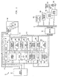
- Referring to Fig. 1 in more detail, a microprocessor control system, generally indicated as 11, which is preferably intended to control a family of thermal printing and ink jet postage meters (not shown), is comprised of a
microprocessor 13 in bus communication (viadata bus 17 and address bus 18 )with an application specific integrated circuit (ASIC) 15 and a plurality of memory units (MU). The ASIC 15 is comprised of a number of integrated circuits, for example,ASIC signal manager 19,address decoder 20,clock 1100,timer module 600, UARTmodule 300, user I/O 1200, keyboard anddisplay interface 1000,interrupt control 700, encryption anddecryption engine 800,memory controller 400, multi-PWM generator andsensor interface 500, aslogan interface 200 andCCD interface 1250. It should be appreciated that it is within the contemplation of the present invention that the integrated circuit modules which make up theASIC 15 may vary and the modules here identified are intended to illustrate the preferred embodiment of the invention. - The ASIC has an internal data bus (IDB) and a plurality of control lines (CL), one group of which control lines are module interrupt lines (IR). Certain of the modules are in communication with a
buffer 50 via I/O lines. Thebuffer 50 is in communication with acoupler 23. Thecoupler 23 is in communication with various meter devices, such as the keyboard and display (KDI), printhead buffer (PHB) andmotor drivers 550 which driverespective motors 552. In Fig. 1, the bus lines IDB, control lines IR and CL and I/O lines are depicted in simplified manner for clarity. - Referring to Fig. 2, the
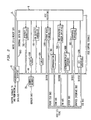
microprocessor 13, in the preferred embodiment, is a Motorola Model MC68EC000 which passes the control signals set forth in Table 1 between themicroprocessor 13 and themicroprocessor interface circuit 19 of the ASIC along the I/O bus CL.Asynchronous Bus Control AS Address Strobe R/W Read/Write Signal UDS Upper Data Strobe LDS Low Data Strobe DTACK Data Transfer Acknowledge Interrupt control IPL0, IPL1, LPL2 Interrupt Priority Level Processor Status Controls FC0, FC1 & FC2 Function Codes System Control BERR Bus Error RESET Reset - The control system address bus is received by the
ASIC address decoder 20 which generates the necessary control signal on the internal ASIC control bus IR for enabling the respective control modules in accordance with the address instruction from themicroprocessor 13. Low order data from thesystem data bus 17 is received by theinterface 19 and placed on the internal data bus of the ASIC to be placed in theASIC registers 8, when enabled by the address decoder. The address enables writing into theASIC registers 8 in response to an address instruction from the microprocessor. The data placed in theASIC registers 8 are the operating parameters or mode selection data for the respective control modules to be accessed by the respective module when the respective module has been enabled by theaddress decoder 20 to generate respective control signals. - Referring to Fig. 3, in order to configure the
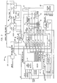
ASIC 15 for a particular meter control system application, it will be necessary to set theaddress decoder 20 relative to the addressable space of the memory units forming part of the system. The address strobe (AS) output from themicroprocessor 13 is directed to amemory decoder section 28 and throughinverter 90 to anAND gate 71 associated with the illegaladdress detection circuit 70 of the system. Thedecoder 28 also communicates with the address bus 17 (address bus lines 23-20, 19-12) to receive 12-bit address information from themicroprocessor 13. Also provided is a memory over-write comparator circuit (OVR) 30 andfunction decoder unit 32. - The output from the
memory size register 24 is carried by the 8-bit internal bus "A" and the output from thedecoder 28 is carried by the 8 bit-internal bus "'B". The respective input to each of a plurality ofcomparators 35 through 42 is in communication with internal bus A and internal bus B. The output ofcomparator 35 is directed to ANDgates comparator 36 is directed to anOR gate 45. The output fromcomparator 44 is internally directed to the ROM pin 46 of the ASIC. The output of theOR gate 45 is internally directed to the RAM pin 48 of the ASIC. The output fromcomparators ASIC pins 50 and 52, and are intended to provide a memory write-enable signal for external devices which may be connected to the control system. The output ofcomparators - A control signal OVR, from the microcontroller, is directed to the input side of the
overlay comparator chip 30 and enables accessing of the memory size supplied from thedecoder 28 of the memory overlay block. The function of ROM-RAM enabled is to designate whether the operating program is in a data transfer or program fetch mode to enable by the microprocessor to utilize the same address range depending on the state of control signals "FC0", "FC1" and "FC2". The control signals "FC0", "FC1" and "FC2" are directed, from the microcontroller, to the input side of afunction decoder 32. The outputs from theoverlay comparator circuit 30 and thefunction decoder 32 are directed toAND gate 60 which has an output directed to the inverse input ofgate 44 and input ofgate 43. The output ofcomparator 42 is directed to the input of anASIC decoder 62. The output of theASIC decoder 62 is used for providing internal addressing of theASIC 15. A control output of the ASIC 62 is directed to the MSR 24 which enables the memory size registers for writing during system power-up. - Referring again to the
comparators 37 through 41,gates OR gate 64 which has an output designated "DTACK" when any of the comparators output goes active. Also the output from eachcomparator Wait Generator 66. The output of theWait Generator 66 is directed to thegate 65 and to theillegal address detector 70. TheWait Generator 66 outputs, when active, delays the issuance of the DTACK signal for a programmed period of time and also suppresses theillegal address detector 70 for the same amount of time. The purpose of delaying the DTACK is based on the fact that the write time for external devices may be protracted. Therefore, to avoid that the microprocessor terminate the bus cycle, the issuing of the DTACK signal is delayed an appropriate amount of time. - An illegal address detection circuit, generally indicated as 70 is provided and includes a
gate 71 which receives the Reset signal from theinterface circuit 19, the address strobe (AS\) signal from the microprocessor and the DTACK signal from thegate 65. Therefore, if an address in an illegal range has been issued, there will not be a DTACK signal issued causing the output of thegate 70 to go active informing theprocessor interface 19 of a bus error. It should be appreciated that theprocessor interface 19 in combination with the subsequently described interruptcontroller 700 is charged with communicating the proper interrupt to themicroprocessor 13. A more detailed description is presented in US Patent Application Serial Number 08/163,790, titled "Address Decoder With Memory Allocation For A Micro-Controller System, commonly assigned. - Referring to Fig. 4, as noted, the meter control system utilizes non-volatile memories to store critical account data. In order to accommodate different type of non-volatile memory which require varying data bus access time, the ASIC includes a dual wait state circuitry. The
Wait Generator 66 is comprised of anNAND gate 1902 having the chip select signals NVM1, NVM2 and NVM3 as inputs. The output of theNAND gate 1902 is directed to the input ofNAND 1904. the output fromNAND gate 1902 is also directed to the data input to the flip-flop 1906. The system clock signal is also directed to the clock input of the flip-flop 1906. The system clock signal is also directed to the clock input of a flip-flop 1908. The data input to the flip-flop 1908 receives the high output from the flip-flop 1906. The high output from the flip-flop 1908 is directed to the other input ofNAND gate 1904. It is observed that if either chip select signal NVM1_B, NVM2_B or NVM3_B (_B signals are active low) goes active the output from theNAND gate 1902 goes high. However, the presence of flip-flops delays NAND gate 1904 from going active for a delay period sufficient to assure adequate time for a write to the non-volatile memories by delaying the issuance of the DTACK signal to thesignal manager 19. The delay time is a function of the type and number of flip-flops - When
NAND gate 1904 goes active,NAND gate 1910 goes active to cause ORgate 1914 to go active. WhenOR gate 1914 goes active ANDgate 1916 goes active. The output of ANDgate 1916 is directed to the data input of a flip-flop 1918 which results in the flip-flop 1918 issuing the DTACK signal. As earlier noted, the DTACK signal is also issued when either the CS1, CS2, RAM, ROM and ASIC chip select signals are active. When either the CS1, CS2, RAM or the ROM signal is active,NAND gate 1912 is active which brings OR 1914 active and causing the DTACK signal to be issued as afore described. It is noted that as afore noted, when the CS1 or CS2 goes active the DTACK signal is delayed unit the WAIT signal goes inactive. A more detailed description is presented in the European application corresponding to US Patent Application Serial Number 08/163,812, titled "ADDRESS DECODER WITH MEMORY WAIT STATE CIRCUIT. - Referring to Fig. 5, in order to match the ASIC system clock, the
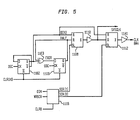
clock module 1100 is programmable, theclock module 1100 includes a first flip-flop 1102 having its high output directed to anXOR gate 1103. The low output of the flip-flop 1102 is directed back to the data input of that flip-flop. The system oscillator is directed to the clock input of flip-flop 1102. The high output from flip-flop 1102 is also directed to one input of amultiplex switch 1108 and amultiplex switch 1112. The output from the XOR gate 1104 is directed to the data input of a flip-flop 1106 which also receives the oscillating signal at its clock input. The high output from the flip-flop 1106 is directed to the other input of theXOR gate 1103 and the other input of themultiplex switch 1108. A clock reset is directed to the resets of both flip-flops - The output from the
multiplex switch 1108 is directed to aamplifier 1110 whose output is designated as system clock for the system clock use and is also directed to the other input of themultiplex switch 1112. Theoutput multiplex switch 1112 is directed to anamplifier 1141 whose output is designated as theclock 8 megahertz. Included are aregister 1116 having a data input, write input and a clear input. One of the outputs from theregister 1116 is directed to themultiplex switch 1108 and the other output is directed to themultiplex switch 1112. - It is now observed that upon power-up of the system, the microprocessor causes a write to the
registers 1116 and other registers of the ASIC registers 8 by addressing theaddress decoder module 20 which then write enables theregister 1116 in a conventional manner. The microprocessor puts the appropriate data on the data lines for writing into theregister 1116 in a customary manner. Depending on the data write, the output from the registers places the multiplex switches in the appropriate switching position to drive the clock frequencies set forth in Table 2 depending on the frequency of the oscillating crystal, as specifically indicated in Table 2.CRYSTAL SCR SYSCLK CLK 8MHz b0 b1 32MHz 0 0 16MHz 16MHz 0 1 8MHz 8MHz 1 0 16MHz 8MHz 1 1 8MHz 4MHz 16MHz 0 0 8MHz 8MHz 0 1 4MHz 4MHz 1 0 8MHz 4MHz 1 1 4MHz 2MHz - Therefore, it is observed that with any given crystal frequency, one will achieve the clock frequencies indicated in Table 2 under the system clock column or the
clock 8 MHz column. As a result, the system offers the advantage of allowing the ASIC to be utilized with larger systems by replacing the crystal with a 32MHz crystal to receive 16MHz and 4MHz signals or utilizing a 16MHz clock to get 8MHz or 4MHz clocking frequency combinations. - It should now be appreciated that the control parameters of a module may be set when the microprocessor writes to the ASIC registers. The above description represents the preferred embodiment and should not be viewed as limiting. The scope of the invention is presented in the claims.
Claims (7)
- A control system for generating control signals to control electrical components of an electronic postage meter having:a programmable microprocessor (13) in bus communication with a plurality of memory units (MU), and an integrated circuit (15), ASIC (15), having an address decoding module (20), clock module (1100) for generating a system clock signal, a timer module (600) for generating a timer signal and a plurality of control modules (400,700,1300) for generating respective component control signals;said address decoding module (20) having means for generating a unique combination of memory control signals in response to a respective address placed on said bus by said microprocessor (13);said memory units being enabled for reading and writing of data from and to said memory units in response to respective ones of said memory control signals from said address decoding module (20);said integrated circuit having a plurality of registers (8) for receiving data generated by said microprocessor (13) in response to respective ones of said memory control signals; andsaid control modules being enabled in response to an address instruction from said microprocessor to read said data from selected ones of said registers (8) such that each control module generates component control signals in accordance with said data.
- A control system according to Claim 1, wherein one of said memory units is a program memory and others of said memory units are non-volatile memory units.
- A control system as claimed in claim 1 or 2 wherein said clock module (1100) has means to read said data from selected ones of said registers and generate a clock signal in accordance with said data.
- A control system as claimed in claim 1, 2 or 3 wherein said timer module has means to read said data from selected ones of said registers and generate a timer signal in accordance with said data.
- A control system as claimed in any preceding claim wherein said address decoder (20) further includes means for partitioning said memory units into valid addressable regions in response to said data in ones of said registers (8).
- A control system as claimed in any preceding claim wherein said microprocessor (13) includes means for receiving a data transfer acknowledge signal and said ASIC having means of generating said data transfer acknowledge signal, said ASIC having means for delaying generation of said data transfer acknowledge signal when said address instruction from said microprocessor directs one of said non-volatile memories to be enabled.
- An electronic postage meter or mailing machine system comprising a control system according to any preceding claim.
Applications Claiming Priority (2)
| Application Number | Priority Date | Filing Date | Title |
|---|---|---|---|
| US08/163,629 US5552991A (en) | 1993-12-09 | 1993-12-09 | Control system for an electronic pastage meter having a programmable application specific intergrated circuit |
| US163629 | 1993-12-09 |
Publications (2)
| Publication Number | Publication Date |
|---|---|
| EP0657817A1 EP0657817A1 (en) | 1995-06-14 |
| EP0657817B1 true EP0657817B1 (en) | 2002-04-03 |
Family
ID=22590861
Family Applications (1)
| Application Number | Title | Priority Date | Filing Date |
|---|---|---|---|
| EP94119503A Revoked EP0657817B1 (en) | 1993-12-09 | 1994-12-09 | Control system for an electronic postage meter having a programmable application specific integrated circuit |
Country Status (4)
| Country | Link |
|---|---|
| US (1) | US5552991A (en) |
| EP (1) | EP0657817B1 (en) |
| CA (1) | CA2137495C (en) |
| DE (1) | DE69430292T2 (en) |
Families Citing this family (11)
| Publication number | Priority date | Publication date | Assignee | Title |
|---|---|---|---|---|
| US5974402A (en) * | 1993-12-09 | 1999-10-26 | Pitney Bowes Inc. | Address decoder with memory wait state circuit |
| US5634044A (en) | 1994-07-29 | 1997-05-27 | Pitney Bowes Inc. | Charge coupled device control module |
| US5664123A (en) | 1994-09-06 | 1997-09-02 | Pitney Bowes Inc. | Digital communication I/O port |
| US5680403A (en) * | 1995-12-14 | 1997-10-21 | Pitney Bowes Inc. | Multiplex serial data communications with a single UART for a postage meter mailing machine system |
| US6226559B1 (en) * | 1995-12-14 | 2001-05-01 | Pitney Bowes Inc. | Method of providing real time machine control system particularly suited for a postage meter mailing machine |
| DE59710554D1 (en) * | 1996-01-31 | 2003-09-18 | Francotyp Postalia Ag | franking machine |
| US5793235A (en) * | 1996-02-13 | 1998-08-11 | Hughes Electronics Corporation | Circuit for improving timing conditions in a data processing unit |
| US6050486A (en) * | 1996-08-23 | 2000-04-18 | Pitney Bowes Inc. | Electronic postage meter system separable printer and accounting arrangement incorporating partition of indicia and accounting information |
| DE19647407C2 (en) * | 1996-11-15 | 1998-09-03 | Siemens Ag | Control device, in particular for use in a motor vehicle |
| US6039257A (en) * | 1997-04-28 | 2000-03-21 | Pitney Bowes Inc. | Postage metering system that utilizes secure invisible bar codes for postal verification |
| US6345875B1 (en) * | 1999-01-19 | 2002-02-12 | Xerox Corporation | Field programmable print control |
Family Cites Families (12)
| Publication number | Priority date | Publication date | Assignee | Title |
|---|---|---|---|---|
| US4644498A (en) * | 1983-04-04 | 1987-02-17 | General Electric Company | Fault-tolerant real time clock |
| US4638452A (en) * | 1984-02-27 | 1987-01-20 | Allen-Bradley Company, Inc. | Programmable controller with dynamically altered programmable real time interrupt interval |
| CA1265255A (en) * | 1986-07-31 | 1990-01-30 | John Polkinghorne | Application specific integrated circuit |
| US5097437A (en) * | 1988-07-17 | 1992-03-17 | Larson Ronald J | Controller with clocking device controlling first and second state machine controller which generate different control signals for different set of devices |
| JP3046310B2 (en) * | 1988-09-13 | 2000-05-29 | 株式会社東芝 | Memory system |
| JP3024767B2 (en) * | 1989-08-29 | 2000-03-21 | 株式会社日立製作所 | Address supply system |
| US5121327A (en) * | 1989-10-18 | 1992-06-09 | Pitney Bowes Inc. | Microcomputer-controlled electronic postage meter having print wheels set by separate d.c. motors |
| US5396599A (en) * | 1990-01-16 | 1995-03-07 | Nec Electronics, Inc. | Computer system with a bus controller |
| FR2664407B1 (en) * | 1990-07-04 | 1992-09-11 | Alcatel Satmam | MACHINE FOR POSTALING MAIL, COMPRISING A SPECIFIC INTEGRATED CIRCUIT CONSTITUTING INTERFACES. |
| US5263139A (en) * | 1992-05-19 | 1993-11-16 | Sun Microsystems, Inc. | Multiple bus architecture for flexible communication among processor modules and memory subsystems and specialized subsystems |
| US5418924A (en) * | 1992-08-31 | 1995-05-23 | Hewlett-Packard Company | Memory controller with programmable timing |
| US5438519A (en) * | 1993-02-10 | 1995-08-01 | Pitney Bowes Inc. | Electronic postage meter having memory write access second chance hard timer means |
-
1993
- 1993-12-09 US US08/163,629 patent/US5552991A/en not_active Expired - Fee Related
-
1994
- 1994-12-07 CA CA002137495A patent/CA2137495C/en not_active Expired - Fee Related
- 1994-12-09 DE DE69430292T patent/DE69430292T2/en not_active Revoked
- 1994-12-09 EP EP94119503A patent/EP0657817B1/en not_active Revoked
Also Published As
| Publication number | Publication date |
|---|---|
| US5552991A (en) | 1996-09-03 |
| EP0657817A1 (en) | 1995-06-14 |
| CA2137495A1 (en) | 1995-06-10 |
| DE69430292D1 (en) | 2002-05-08 |
| CA2137495C (en) | 1998-08-18 |
| DE69430292T2 (en) | 2002-11-21 |
Similar Documents
| Publication | Publication Date | Title |
|---|---|---|
| US4858138A (en) | Secure vault having electronic indicia for a value printing system | |
| EP0657817B1 (en) | Control system for an electronic postage meter having a programmable application specific integrated circuit | |
| EP0657823A2 (en) | Memory access protection circuit with encryption key | |
| EP0572668B1 (en) | Apparatus and method for processing information, and additional control device used therein | |
| US5920850A (en) | Metering system with automatic resettable time lockout | |
| US5729716A (en) | Memory monitoring circuit for detecting unauthorized memory access | |
| EP0657822B1 (en) | Multi-access limiting circuit for a multi-memory device | |
| EP0657854B1 (en) | Programmable clock module for postage metering control system | |
| US5974402A (en) | Address decoder with memory wait state circuit | |
| EP0657791B1 (en) | Dynamically programmable timer-counter | |
| CA2152836C (en) | Control system for an electronic postage meter having a programmable print head controller | |
| EP0658846A1 (en) | Address decoder with memory allocation for a micro-controller system | |
| US5475621A (en) | Dual mode timer-counter | |
| EP0658847A1 (en) | Address decoder with memory allocation and illegal address detection for a microcontroller system | |
| EP0657806A1 (en) | Interrupt controller for an integrated circuit | |
| CA2154380C (en) | Charge coupled device control module | |
| CA1250052A (en) | Electronic postage meter having a memory map decoder |
Legal Events
| Date | Code | Title | Description |
|---|---|---|---|
| PUAI | Public reference made under article 153(3) epc to a published international application that has entered the european phase |
Free format text: ORIGINAL CODE: 0009012 |
|
| AK | Designated contracting states |
Kind code of ref document: A1 Designated state(s): CH DE FR GB LI |
|
| 17P | Request for examination filed |
Effective date: 19950804 |
|
| 17Q | First examination report despatched |
Effective date: 19991221 |
|
| GRAG | Despatch of communication of intention to grant |
Free format text: ORIGINAL CODE: EPIDOS AGRA |
|
| GRAG | Despatch of communication of intention to grant |
Free format text: ORIGINAL CODE: EPIDOS AGRA |
|
| GRAH | Despatch of communication of intention to grant a patent |
Free format text: ORIGINAL CODE: EPIDOS IGRA |
|
| GRAH | Despatch of communication of intention to grant a patent |
Free format text: ORIGINAL CODE: EPIDOS IGRA |
|
| REG | Reference to a national code |
Ref country code: GB Ref legal event code: IF02 |
|
| GRAA | (expected) grant |
Free format text: ORIGINAL CODE: 0009210 |
|
| AK | Designated contracting states |
Kind code of ref document: B1 Designated state(s): CH DE FR GB LI |
|
| REG | Reference to a national code |
Ref country code: CH Ref legal event code: NV Representative=s name: E. BLUM & CO. PATENTANWAELTE Ref country code: CH Ref legal event code: EP |
|
| REF | Corresponds to: |
Ref document number: 69430292 Country of ref document: DE Date of ref document: 20020508 |
|
| ET | Fr: translation filed | ||
| PLBQ | Unpublished change to opponent data |
Free format text: ORIGINAL CODE: EPIDOS OPPO |
|
| PLBI | Opposition filed |
Free format text: ORIGINAL CODE: 0009260 |
|
| PLBF | Reply of patent proprietor to notice(s) of opposition |
Free format text: ORIGINAL CODE: EPIDOS OBSO |
|
| 26 | Opposition filed |
Opponent name: FRANCOTYP-POSTALIA AKTIENGESELLSCHAFT & CO. KG Effective date: 20030103 |
|
| PLBF | Reply of patent proprietor to notice(s) of opposition |
Free format text: ORIGINAL CODE: EPIDOS OBSO |
|
| RDAF | Communication despatched that patent is revoked |
Free format text: ORIGINAL CODE: EPIDOSNREV1 |
|
| APBP | Date of receipt of notice of appeal recorded |
Free format text: ORIGINAL CODE: EPIDOSNNOA2O |
|
| APBQ | Date of receipt of statement of grounds of appeal recorded |
Free format text: ORIGINAL CODE: EPIDOSNNOA3O |
|
| APAA | Appeal reference recorded |
Free format text: ORIGINAL CODE: EPIDOS REFN |
|
| APAH | Appeal reference modified |
Free format text: ORIGINAL CODE: EPIDOSCREFNO |
|
| PGFP | Annual fee paid to national office [announced via postgrant information from national office to epo] |
Ref country code: FR Payment date: 20061220 Year of fee payment: 13 |
|
| PGFP | Annual fee paid to national office [announced via postgrant information from national office to epo] |
Ref country code: GB Payment date: 20061222 Year of fee payment: 13 |
|
| PGFP | Annual fee paid to national office [announced via postgrant information from national office to epo] |
Ref country code: CH Payment date: 20061227 Year of fee payment: 13 |
|
| PGFP | Annual fee paid to national office [announced via postgrant information from national office to epo] |
Ref country code: DE Payment date: 20070131 Year of fee payment: 13 |
|
| APBU | Appeal procedure closed |
Free format text: ORIGINAL CODE: EPIDOSNNOA9O |
|
| RDAG | Patent revoked |
Free format text: ORIGINAL CODE: 0009271 |
|
| STAA | Information on the status of an ep patent application or granted ep patent |
Free format text: STATUS: PATENT REVOKED |
|
| 27W | Patent revoked |
Effective date: 20070316 |
|
| GBPR | Gb: patent revoked under art. 102 of the ep convention designating the uk as contracting state |
Free format text: 20070316 |
|
| REG | Reference to a national code |
Ref country code: CH Ref legal event code: PL |