EP0665696A2 - Digital video signal processing device and tv camera device arranged to use it - Google Patents
Digital video signal processing device and tv camera device arranged to use it Download PDFInfo
- Publication number
- EP0665696A2 EP0665696A2 EP95300556A EP95300556A EP0665696A2 EP 0665696 A2 EP0665696 A2 EP 0665696A2 EP 95300556 A EP95300556 A EP 95300556A EP 95300556 A EP95300556 A EP 95300556A EP 0665696 A2 EP0665696 A2 EP 0665696A2
- Authority
- EP
- European Patent Office
- Prior art keywords
- signal
- video signal
- clipping
- interpolation data
- clipped
- Prior art date
- Legal status (The legal status is an assumption and is not a legal conclusion. Google has not performed a legal analysis and makes no representation as to the accuracy of the status listed.)
- Granted
Links
Images


Classifications
-
- H—ELECTRICITY
- H04—ELECTRIC COMMUNICATION TECHNIQUE
- H04N—PICTORIAL COMMUNICATION, e.g. TELEVISION
- H04N9/00—Details of colour television systems
- H04N9/64—Circuits for processing colour signals
- H04N9/68—Circuits for processing colour signals for controlling the amplitude of colour signals, e.g. automatic chroma control circuits
-
- G—PHYSICS
- G06—COMPUTING; CALCULATING OR COUNTING
- G06T—IMAGE DATA PROCESSING OR GENERATION, IN GENERAL
- G06T9/00—Image coding
- G06T9/004—Predictors, e.g. intraframe, interframe coding
-
- H—ELECTRICITY
- H04—ELECTRIC COMMUNICATION TECHNIQUE
- H04N—PICTORIAL COMMUNICATION, e.g. TELEVISION
- H04N9/00—Details of colour television systems
- H04N9/64—Circuits for processing colour signals
- H04N9/646—Circuits for processing colour signals for image enhancement, e.g. vertical detail restoration, cross-colour elimination, contour correction, chrominance trapping filters
Definitions
- the present invention relates to a digital video signal processing device and more particularly to a TV camera device which is arranged to use the processing device.
- an imaging device such as a TV camera provides a signal output level defined in a specified range from the maximum to the minimum level.
- a video signal level may go higher or lower than the specified range.
- the imaging device has a circuit for clipping a signal of higher or lower signal level than the specified range for suppressing the output signal level inside of the specified range. This circuit is generally referred to as a white clipping circuit or a black clipping circuit.
- the similar clipping means is required to suppress the output signal level inside of the specified range.
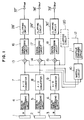
- Fig. 1 shows a conventional arrangement of a TV camera with processing a digital video signal.
- numerals 1 to 3 denote an image pickup element.
- Numerals 4 to 6 denote an analog signal processing circuit, which performs necessary signal treatments such as signal amplification and band restriction with respect to R, G and B video signals picked up from the image pickup elements 1 to 3.
- Numerals 7 to 9 denote an analog-to-digital converter, which operates to convert the output of the analog signal processing circuit 4, 5 or 6 into a digital signal.
- the digitized R, G and B signals outputted from the analog-to-digital converters 7-9 are sent to a matrix circuit 10 in which those signals are mixed at a predetermined ratio. Then, the mixed signal is inputted to a contour emphasis circuit 11 in which a contour emphasis signal 12 is produced from the mixed signal.
- a contour emphasis signal 12 higher than the predetermined signal level is clipped by a clipping circuit 120 which may be provided if necessary. Then, the clipped signal is added to each of the R, G and B signals in an adding circuit 13, 14 or 15.
- the R, G and B signals to which the contour emphasis signal 12 is added are processed in a signal processing circuit 16, 17 or 18. This processing is gamma correction or the like.
- the outputs of the signal processing circuits 16 to 18 are sent to clipping circuits 28' to 30', respectively.
- Those clipping circuits 28' to 30' operate to clip the signals deviated from the specified range and output the clipped signals as Rout 37', Gout 38' and Bout 39', respectively.
- Each signal is sent to a matrix circuit (not shown) in which the clipped signals are converted into a luminance signal Y and color difference signals I and Q.
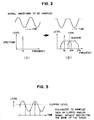
- Figs. 2 and 3 are views for explaining why the aliasing distortion is caused by digital signal processing.
- the continuous analog signal is sampled at fixed intervals.
- this digitizing may bring about the aliasing distortions, that is, the low frequency portions converted from higher harmonic components.
- the occurrence of such aliasing distortions are allowed to be prevented by restricting frequency band of an analog signal within a half or less sampling frequency before sampling. This is a well-known Nyquist condition.
- a signal to be sampled (that is, an original analog signal) is a sine wave signal (see (A) of Fig. 2) of such a frequency fs as satisfying the Nyquist condition before clipping
- the clipping of the signal to keep the predetermined signal level results in causing the clipped signal to be mixed with higher harmonic components of an integer (n) time greater frequency than the original signal, that is, a frequency n ⁇ fs (see (B) of Fig. 2).
- n integer
- the clipped signal containing higher harmonic components is sampled without any band restriction, higher harmonic components having a higher frequency than a half of a sampling frequency fc are converted into low-frequency portions, which conversion brings about the aliasing distortion.
- the sampled signal (without any band restriction), that is, the digitized video signal which is no operated to clip with analog signal process is clipped with digital signal process
- this is equivalent to sampling of the signal which is operated to clip with analog process without any band restriction as described above, which thus brings about the aliasing distortion.
- the value of each sampling point is converted into a value at the clipping level as shown in Fig. 3.
- interpolation For a TV camera system required to do the above-mentioned clipping process, a technique for preventing occurrence of the aliasing distortion by utilizing process of interpolation as described in JP-A-4-152779 has been known.
- interpolation used throughout this specification means a pseudo-interpolation wherein the calculation operation is made at each of intermediate points in a finite number between sampling points.
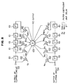
- Fig. 4 shows a block arrangement in which the technique disclosed in JP-A-4-152779 is applied to a signal level restricting circuit corresponding to the clipping circuit of Fig. 1 included in the signal processing section of a TV camera.
- Fig. 5 shows the relation between the original input data, that is, the data to be interpolated and the interpolation data.
- Each of the data interpolating circuits 25 to 27 performs an interpolating process with respect to an input signal (referred to as original data signal) sampled from an original analog signal at periods T indicated by X marks of Fig. 5, for generating interpolation data indicated by circles of Fig. 5 located at a middle point of each sampling period T of the original data, for example.
- This process of interpolation offers an up-converted and interpolated signal having twice as high a rate as the original data signal, that is, a signal sampled at a half of the period T, which signal is composed of the original data signal and the interpolation data signal.
- an interpolation data value given in the data interpolating circuits 25 to 27 can be presumed by calculating an output provided by means that a delta function series signal passes through an ideal low-pass filter having the Nyquist frequency corresponding to a half of the sampling period T.
- a delta function series signal represents a discrete sampled signal. This presumption, however, requires an enormous amount of data.
- a finite degree digital filter is used for presuming the value with doing a predicting coding process. This finite degree digital filter is arranged of delay elements 41, multipliers 42 and an adder 43 in Fig. 6.
- Each of the filter coefficient values C0 to C 2n-1 given to the multiplier 42 may be a designed value of a transversal type digital filter having a half of a sampling frequency fc as a cut-off frequency.
- n 2
- C1 or C2 0.625
- the outputs of the data interpolating circuits 25 to 27 are applied to the clipping circuits 28 to 30 in which the signals staying higher or lower than the specified signal level are clipped within the predetermined signal level.
- the clipping of the signals in the clipping circuits 28 to 30 causes higher harmonic components to be generated.
- the frequency of the higher harmonic components in a range of a half of or the same as the (original) sampling frequency before up-converting is made to be in a range of a half or less time as large a value as the up-converted sampling frequency, that is, doubled sampling frequency.
- the higher harmonic components generated in the frequency range are not made to be the aliasing distortion while the signal is up-converted as mentioned above.
- the low-pass filter has a cut-off frequency set as a quarter of the up-converted sampling frequency and a half of the sampling frequency before the up-conversion.
- Each output of the low-pass filters 31 to 33 is applied to the corresponding one of thinning circuits 34 to 36 in which every other piece of data is thinned out for returning the up-converted signal into a digital signal having the same sampling rate as the original data signal. Then, the digital signal is outputted to the later stage (not shown).
- this prior art arranged to use the technique disclosed in JP-A-4-152779 operates to clip the digital signal up-converted by an interpolating process. If this clipping process brings about the higher harmonic components, these higher harmonic components fill the foregoing Nyquist condition, and no aliasing distortion takes place with respect to them. This means that this type of harmonic components the frequency of which are higher than of a data signal are allowed to be removed by a low-pass filter without missing the data signal. Thus, the digital signal processing device enables to clip a digital signal without having to bring about any aliasing distortion.
- the contour emphasis signal 12 outputted from the contour emphasis circuit 11 is restricted in level through the effect of the circuits equivalent to the signal level restricting circuits 19' to 21'.
- the present invention provides a digital video signal processing device which enables to reduce or prevent occurrence of an aliasing distortion without having to do up conversion of a digital signal and without digital processing use a higher speed (frequency) clock signal.
- a digital video signal processing device includes an interpolation data generating unit for generating an interpolation data signal corresponding to an intermediate point between the adjacent sampling points of a digital video signal, a clipping unit for clipping the interpolation data signal generated and outputted by the interpolation data generating unit and the original digital video signal to an upper or a lower limit value, and a synthesizing unit for performing a predictive coding operation with respect to each clipped signal and synthesizing the coded signals together.
- the synthesizing unit contained in the device according to the first aspect of the invention operates to perform a predictive coding operation with respect to any one of the clipped original video signal and the clipped intermediate data signal and synthesizing the coded signal and the in-coded signal.
- a digital video signal processing device includes a unit for generating a digital contour emphasis signal from digitized R, G and B video signals and a first clipping unit for clipping the contour emphasis signal to a predetermined upper limit value or a lower limit value, an interpolation data generating unit for generating interpolation data signal corresponding to an intermediate point of a sampling period from the contour emphasis signal before it is not clipped, and a second clipping unit for clipping the interpolation data signal to the predetermined upper or lower limit value, in which the output of one clipping unit is added to the G signal for one contour emphasis signal and the output of the other clipping unit is added to the R and the B signals for the other one.
- the interpolation data generating unit operates to generate an interpolation data signal.
- the clipping units operate to clip the original digital video signal or the interpolation data signal, respectively. These operations result in bringing about higher harmonic components having a half or more of a sampling frequency, thereby causing the aliasing distortion.
- the phase of the aliasing distortion components generated by clipping the original digital video signal is equivalently axial-symmetric with respect to the phase of the aliasing distortion components generated by clipping the interpolation data signal in light of the sampling theorem. Considering such symmetric phase relation, the predicting coding and the synthesis of the original digital video signal and the interpolation data signal clipped by the synthesizing unit make it possible to offset the aliasing distortions in reverse phase and thereby cancel them.
- the synthesizing unit operates to perform a predictive coding operation with respect to any one of the original digital video signal and the interpolation data signal and synthesizing the coded signal and the in-coded signal. This operation simplifies the arrangement of the digital filtering unit for performing a predictive coding operation in comparison with the arrangement according to the first aspect of the invention.
- the sampling phase of one contour emphasis signal added to the G signal which occupies about a half of luminance signal components, is axial-symmetric with respect to that of the other contour emphasis signal added to the R and B signals.
- the aliasing distortion caused by the first or even degree higher harmonic component of one contour emphasis signal is reverse in phase to that of the other contour emphasis signal.
- the R, G and B signals are mixed with one another for producing a luminance signal, it is equivalent to the addition of the aliasing distortions in reverse phase at the similar ratios. This results in cancelling the aliasing distortions, thereby eliminating the adverse effect of the aliasing distortions on image quality at the later stages of the video signal processing device.
- the signal clip also brings about even degree higher harmonic components and thereby the relevant aliasing distortions. Though those kinds of aliasing distortions are not cancelled, those higher harmonic components are so low at the level that they hardly have an adverse effect on the quality of the resulting image. Hence, those even degree higher harmonic components may be ignored.
- This embodiment is arranged to improve the drawbacks of the foregoing prior art and enables to clip a reducing or preventing occurrence of aliasing distortion, without having to enhance the operating frequency on which a digital signal is processed.
- R, G and B video signals picked up from image pickup elements 1 to 3 are sent to analog signal processing circuits 4 to 6 in which necessary treatments such as amplification and band restriction are performed with respect to those video signals.
- the processed signals are converted into digital signals through the effect of analog-to-digital converters 7 to 9.
- the converted digital R, G and B signals are sent to a matrix circuit 10 in which those signals are mixed at a predetermined ratio.
- the mixed output of the matrix circuit 10 is applied to a contour emphasis circuit 11 for producing a contour emphasis signal 12.
- the contour emphasis signal 12 is sent to adding circuits 13 to 15 in which the signal is added to the corresponding one of the R, G and B signals.
- the R, G and B signals each having the contour emphasis signals added thereto are sent to signal processing circuits 16 to 18 in which some treatments such as gamma correction process are carried out.
- the processed signals are sent to signal level restriction circuits 19 to 21.
- An interpolation data generating unit 52 is used to generate interpolation data signal from the inputted digital video signal 51.
- the interpolation data generating unit 52 is equivalent to a transversal type filter described about the foregoing interpolating circuits 25 to 27.
- the interpolation data signal has a signal level predicted at a middle point between the adjacent sampling points of the inputted digital video signal 51.
- the digital video signal 51 is applied to a delay unit 52' (indicated by a broken line of Fig. 7) for delaying the signal by the delay of the output of the interpolation data generating unit 52.
- the delayed signal is sent to clipping circuit 53, and the interpolation data signal is sent to clipping circuit 54.
- the output of the delay unit 52' and the output of the interpolation data generating unit 52 are clipped to their upper or lower limit values, respectively.
- a group of partial delay elements contained in a transversal type filter composing the unit 52 may be used for the purpose.
- An output of the group of delay elements may be applied to the clipping circuit 53.
- the clipping operation done by the clipping circuits 53 and 54 gives rise to higher harmonic components and the aliasing distortion based on the higher harmonic components.
- the phase of the aliasing distortion caused in the clipped interpolation data signal is equivalently and axial-symmetric with respect to the phase of the aliasing distortion caused in the clipped digital video signal in light of the sampling theorem.
- a synthesizing unit 55 (to be described below) performs a predictive coding operation with respect to the clipped interpolation data signal and the clipped digital video signal and synthesizes these signals with each other. This makes it possible to offset these aliasing distortion components in reverse phase, thereby removing the distortions.
- the output of the clipping circuit 53 is applied to one end of a group of delaying elements 61 serially connected with each other. Each delaying element 61 provides a delayed output at each one clock of a sampling frequency.
- the output of the clipping circuit 53 is applied to one multiplier 62 and the output of each delaying element 62 is applied to another multiplier 62.
- these signals are multiplied by coefficients C0, C1,..., C2m-1 in the earlier sequence of the delaying timing.
- the outputs of these multipliers 62 are applied to an adder 63.
- the output of the clipping circuit 54 is applied to one end of the other group of delaying elements 61 serially connected with each other.
- Each delaying element 61 provides a delayed output at each one clock of the sampling frequency.
- the outputs of the clipping circuit 54 and the delaying elements 61 are applied to their corresponding multipliers 62. In these multipliers, those signals are multiplied by coefficients K0, K1,..., K2n-1 in the earlier sequence of the delaying timing.
- the outputs of those multipliers 62 are applied to the adder 63.
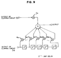
- the aforementioned synthesizing unit 55 operates to perform a predictive coding operation with respect to each of the clipped interpolation data signal and the clipped digital video signal for matching the phases of these signals and to synthesize them with each other. This operation makes it possible to offset the aliasing distortion components reversely phased with each other, thereby eliminating both of the distortion components.
- the clipping operation gives rise to a digital signal with reducing or preventing occurrence of aliasing distortion, without having to enhance the operating frequency on which the digital signal is processed.
- This embodiment is arranged on the assumption that the coefficient C0 is 1/2 and all the coefficients from C1 to C2m-1 except C0 are zero.
- the arrangement as shown in Fig. 9 does not include the delaying circuits and the multipliers located on the side of the output of the clipping circuit 53 except the multiplier for multiplying the output of the clipping circuit 53 by the coefficient C0, which are all included in the arrangement shown in Fig. 8. This results in greatly reducing the arrangement of the signal level restricting circuit.
- Fig. 10 shows an overall signal-processing arrangement of a camera system having a contour emphasis circuit to which the invention is applied. Later, the operation of this embodiment will be discussed in detail.
- the output of the contour emphasis circuit 11 is applied to the clipping circuit 112 and the interpolation data generating circuit 113.
- the interpolation data signal indicated by a circle mark of Fig. 5 is generated at the middle point of the sampling period T by performing an interpolating operation with respect to the contour emphasis signal indicated by an X mark of Fig. 5 (that is, original data) of the period T.
- the middle point is one example. Another intermediate position may be selected.
- the interpolation data value can be ideally obtained by calculating an output which is given when a delta function series signal is passed through a low-pass filter having an ideal Nyquist frequency.
- the delta function series signal corresponds to a discrete sampled signal.
- a definite degree digital filter composed of the delaying elements 41, the multipliers 42, and the adder 43 is used for the purpose.
- Each of the filter coefficients C0 to C2n-1 to be added to the multiplier 42 may be a designed value of the transversal type digital filter having a half of the sampling frequency fc as a cut-off frequency.
- the original contour emphasis signal is applied to a first clipping circuit 112 and the interpolation data signal obtained by the foregoing process is applied to a second clipping circuit 114.
- These signals are clipped in the predetermined range of a signal level. This is based on the characteristic as shown in Fig. 12, for example.
- the clipping operation inevitably gives rise to higher harmonic components having a higher frequency than a half of the sampling frequency fc, which higher harmonic components bring about the aliasing distortion.
- the sampling phase of the original contour signal is axial-symmetric with respect to that of the interpolation data signal.
- the aliasing distortion of the first higher harmonic components existing in the signal issued from the clipping circuit 112 is 180°-reversed in phase with respect to that existing in the signal issued from the clipping circuit 114 but has the substantially same level. That is, both of the signals have the opposite polarities to each other but the same absolute value as each other.
- an aliasing distortion of the first harmonic components is offset with the other aliasing distortion.
- the aliasing distortion of the second or later higher harmonic components has the small level whatever sign it may have. Hence, the second or later higher harmonic components do not have an adverse effect on the resulting image quality.
- the output signal from the first clipping circuit 112 is added to the G signal in the adding circuit 14.
- the signal addition gives the contour emphasis capacity to the G signal.
- the output signal from the second clipping circuit 114 is added to the R signal in the adding circuit 13.
- the same output signal is added to the B signal in the adding circuit 15.
- These adding operations give the contour emphasis capacities to the R and the B signals.
- These G, R and B signals are sent to the signal processing circuits 16 to 18, respectively, in which some treatments such as gamma correction process are performed with respect to those signals.
- the processed G, R and B signals are all applied from the corresponding signal processing circuits 16 to 18 to a matrix circuit 121.
- the matrix circuit 121 operates to mix the processed R, G and B signals with each other at a predetermined ratio for synthesizing a luminance signal Y and color difference signals I and Q.
- the luminance signal Y synthesized in the matrix circuit 121 is applied to an encoder 124.
- the color difference signal I is applied to a low-pass filter 122 and the signal Q is applied to a low-pass filter 123 for restricting the bands of the color difference signals I and Q.
- the band-restricted signals I and Q are applied to the encoder 124.
- the encoder 124 operates to modify the band-restricted color difference signals I and Q with a sub-carrier, overlap the modified signals with the luminance signal Y and output a composite color signal to the later stage (not shown).
- the aliasing distortion contained in the contour emphasis signal added to the G signal which occupies about a half of the luminance signal components, is 180°-reversed in phase to the aliasing distortion contained in the contour emphasis signal added to the remaining R and B signals. Synthesis of these signals results in substantially offsetting the aliasing distortions with each other. Hence, the luminance signal to be outputted to the later stage hardly has aliasing distortion, so that no image degrade caused by the aliasing distortion takes place.
- R:G:B 30:59:11.
- the matrix circuit operates to synthesize the color difference signals I and Q at a different ratio with the ratio of the luminance signal Y, at which the aliasing distortions are not so much offset.
- the aliasing distortions caused by the color difference signals do not have so much more adverse effect on the image quality than that caused by the luminance signal. These thus have a negligible effect on image quality respectively.
- a TV camera system is normally arranged to add the contour emphasis signal to the video signal and then restrict the video signal level through the effect of a white and black clipping circuit or the like.
- This normal kind of TV camera system may have the above-mentioned arrangement. That is, since the phases of the aliasing distortions are reversed to each other, when producing the luminance signal with respect to clipped video signal, the aliasing distortion components of the G and R, B signals are substantially offset with each other.
- the present invention offers a digital video signal processing device which enables to restrict the signal output level by the digitally clipping operation with hardly the aliasing distortion.
- the aliasing distortion components are substantially cancelled without having to filter the luminance signal.
- the cancellation leads to improving the image quality.
Abstract
Description
- The present invention relates to a digital video signal processing device and more particularly to a TV camera device which is arranged to use the processing device.
- In general, an imaging device such as a TV camera provides a signal output level defined in a specified range from the maximum to the minimum level. In some circumstances, however, a video signal level may go higher or lower than the specified range. For example, as mentioned below, when an image is picked up under a large amount of incident light, the video signal level goes higher. On the other hand, when it is done under a small amount of incident light, the video signal level goes lower. Or, a contour emphasis treatment is executed in the device. To overcome this drawback, the imaging device has a circuit for clipping a signal of higher or lower signal level than the specified range for suppressing the output signal level inside of the specified range. This circuit is generally referred to as a white clipping circuit or a black clipping circuit.
- To digitize a video signal when processing it, the similar clipping means is required to suppress the output signal level inside of the specified range.
- Fig. 1 shows a conventional arrangement of a TV camera with processing a digital video signal.
- In Fig. 1,
numerals 1 to 3 denote an image pickup element.Numerals 4 to 6 denote an analog signal processing circuit, which performs necessary signal treatments such as signal amplification and band restriction with respect to R, G and B video signals picked up from theimage pickup elements 1 to 3.Numerals 7 to 9 denote an analog-to-digital converter, which operates to convert the output of the analogsignal processing circuit matrix circuit 10 in which those signals are mixed at a predetermined ratio. Then, the mixed signal is inputted to acontour emphasis circuit 11 in which acontour emphasis signal 12 is produced from the mixed signal. Acontour emphasis signal 12 higher than the predetermined signal level is clipped by aclipping circuit 120 which may be provided if necessary. Then, the clipped signal is added to each of the R, G and B signals in an addingcircuit contour emphasis signal 12 is added are processed in asignal processing circuit signal processing circuits 16 to 18 are sent to clipping circuits 28' to 30', respectively. Those clipping circuits 28' to 30' operate to clip the signals deviated from the specified range and output the clipped signals as Rout 37', Gout 38' and Bout 39', respectively. Each signal is sent to a matrix circuit (not shown) in which the clipped signals are converted into a luminance signal Y and color difference signals I and Q. - However, the foregoing clipping brings about aliasing distortions, the cause of which will be discussed below.
- Later, the description will be oriented to why this aliasing distortion takes place with reference to Figs. 2 and 3. Figs. 2 and 3 are views for explaining why the aliasing distortion is caused by digital signal processing.
- In general, to convert an analog signal into a digital signal, the continuous analog signal is sampled at fixed intervals. Hence, it is to be noted that when the analog video signal is digitized, this digitizing may bring about the aliasing distortions, that is, the low frequency portions converted from higher harmonic components. The occurrence of such aliasing distortions are allowed to be prevented by restricting frequency band of an analog signal within a half or less sampling frequency before sampling. This is a well-known Nyquist condition.
- As shown in Fig. 2, however, if a signal to be sampled (that is, an original analog signal) is a sine wave signal (see (A) of Fig. 2) of such a frequency fs as satisfying the Nyquist condition before clipping, the clipping of the signal to keep the predetermined signal level results in causing the clipped signal to be mixed with higher harmonic components of an integer (n) time greater frequency than the original signal, that is, a frequency n·fs (see (B) of Fig. 2). At a time, if the clipped signal containing higher harmonic components is sampled without any band restriction, higher harmonic components having a higher frequency than a half of a sampling frequency fc are converted into low-frequency portions, which conversion brings about the aliasing distortion.
- In a case that, on the other hand, the sampled signal (without any band restriction), that is, the digitized video signal which is no operated to clip with analog signal process is clipped with digital signal process, this is equivalent to sampling of the signal which is operated to clip with analog process without any band restriction as described above, which thus brings about the aliasing distortion. This will be understood that the value of each sampling point is converted into a value at the clipping level as shown in Fig. 3.
- Hence, if a subject analog signal the frequency band of which is restricted to a half or less of a sampling frequency is sampled, and if the sampled signal (that is, digitized signal) is clipped with digital signal process, this brings about the aliasing distortion as mentioned above.
- For a TV camera system required to do the above-mentioned clipping process, a technique for preventing occurrence of the aliasing distortion by utilizing process of interpolation as described in JP-A-4-152779 has been known. The term "interpolation" used throughout this specification means a pseudo-interpolation wherein the calculation operation is made at each of intermediate points in a finite number between sampling points.
- Later, the concrete arrangement of the technique will be briefly described with reference to the drawings.
- Fig. 4 shows a block arrangement in which the technique disclosed in JP-A-4-152779 is applied to a signal level restricting circuit corresponding to the clipping circuit of Fig. 1 included in the signal processing section of a TV camera.
- Below, the arrangements and the operations of the signal level restricting circuits 19' to 21' will be discussed in detail.
-
Data interpolating circuits 25 to 27 at a first stage will be described with reference to Fig. 5 which shows the relation between the original input data, that is, the data to be interpolated and the interpolation data. - Each of the
data interpolating circuits 25 to 27 performs an interpolating process with respect to an input signal (referred to as original data signal) sampled from an original analog signal at periods T indicated by X marks of Fig. 5, for generating interpolation data indicated by circles of Fig. 5 located at a middle point of each sampling period T of the original data, for example. This process of interpolation offers an up-converted and interpolated signal having twice as high a rate as the original data signal, that is, a signal sampled at a half of the period T, which signal is composed of the original data signal and the interpolation data signal. - Ideally, an interpolation data value given in the
data interpolating circuits 25 to 27 can be presumed by calculating an output provided by means that a delta function series signal passes through an ideal low-pass filter having the Nyquist frequency corresponding to a half of the sampling period T. A delta function series signal represents a discrete sampled signal. This presumption, however, requires an enormous amount of data. Actually, hence, a finite degree digital filter is used for presuming the value with doing a predicting coding process. This finite degree digital filter is arranged ofdelay elements 41,multipliers 42 and anadder 43 in Fig. 6. - Each of the filter coefficient values C0 to C2n-1 given to the
multiplier 42 may be a designed value of a transversal type digital filter having a half of a sampling frequency fc as a cut-off frequency. As a simple example, in the case of n = 2, C1 or C2 = 0.625 and C0 or C3 = -0.125 are given as the filter coefficients. - In order to realize the process of up-converting the data signal in the
data interpolating circuits 25 to 27, as shown in Fig. 6, it is just possible to synchronize the original data and the interpolation data with the sampling period, and alternately output these two data at a half of the sampling period by using aswitch 44. - The outputs of the
data interpolating circuits 25 to 27 are applied to theclipping circuits 28 to 30 in which the signals staying higher or lower than the specified signal level are clipped within the predetermined signal level. - The clipping of the signals in the
clipping circuits 28 to 30 causes higher harmonic components to be generated. The frequency of the higher harmonic components in a range of a half of or the same as the (original) sampling frequency before up-converting is made to be in a range of a half or less time as large a value as the up-converted sampling frequency, that is, doubled sampling frequency. Hence, the higher harmonic components generated in the frequency range are not made to be the aliasing distortion while the signal is up-converted as mentioned above. - Further, these clipped signals are filtered by low-
pass filters 31 to 33 for removing the higher harmonic components. The low-pass filter has a cut-off frequency set as a quarter of the up-converted sampling frequency and a half of the sampling frequency before the up-conversion. - Each output of the low-
pass filters 31 to 33 is applied to the corresponding one of thinning circuits 34 to 36 in which every other piece of data is thinned out for returning the up-converted signal into a digital signal having the same sampling rate as the original data signal. Then, the digital signal is outputted to the later stage (not shown). - As set forth above, this prior art arranged to use the technique disclosed in JP-A-4-152779 operates to clip the digital signal up-converted by an interpolating process. If this clipping process brings about the higher harmonic components, these higher harmonic components fill the foregoing Nyquist condition, and no aliasing distortion takes place with respect to them. This means that this type of harmonic components the frequency of which are higher than of a data signal are allowed to be removed by a low-pass filter without missing the data signal. Thus, the digital signal processing device enables to clip a digital signal without having to bring about any aliasing distortion.
- In the signal level restricting circuits 19' to 21' included in this prior art, however, digital circuits of the imaging device in the interval between the up conversion done by the
data interpolating circuits 25 to 27 and the thinning-out operation done by the thinning circuits 34 to 36 are required to operate at twice as large an operating frequency as the sampling frequency before the up conversion. This may bring about a significant shortcoming in light of cost, power consumption and stability of operation. - According to another conventional technique, the
contour emphasis signal 12 outputted from thecontour emphasis circuit 11 is restricted in level through the effect of the circuits equivalent to the signal level restricting circuits 19' to 21'. - It is an object of the present invention to provide a digital video signal processing device which operates to reduce or prevent occurrence of an aliasing distortion in clipping a digital video signal, for enhancing image quality.
- Preferably the present invention provides a digital video signal processing device which enables to reduce or prevent occurrence of an aliasing distortion without having to do up conversion of a digital signal and without digital processing use a higher speed (frequency) clock signal.
- According to a first aspect of the invention, a digital video signal processing device includes an interpolation data generating unit for generating an interpolation data signal corresponding to an intermediate point between the adjacent sampling points of a digital video signal, a clipping unit for clipping the interpolation data signal generated and outputted by the interpolation data generating unit and the original digital video signal to an upper or a lower limit value, and a synthesizing unit for performing a predictive coding operation with respect to each clipped signal and synthesizing the coded signals together.
- According to a second aspect of the invention, the synthesizing unit contained in the device according to the first aspect of the invention operates to perform a predictive coding operation with respect to any one of the clipped original video signal and the clipped intermediate data signal and synthesizing the coded signal and the in-coded signal.
- According to the third aspect of the invention, a digital video signal processing device includes a unit for generating a digital contour emphasis signal from digitized R, G and B video signals and a first clipping unit for clipping the contour emphasis signal to a predetermined upper limit value or a lower limit value, an interpolation data generating unit for generating interpolation data signal corresponding to an intermediate point of a sampling period from the contour emphasis signal before it is not clipped, and a second clipping unit for clipping the interpolation data signal to the predetermined upper or lower limit value, in which the output of one clipping unit is added to the G signal for one contour emphasis signal and the output of the other clipping unit is added to the R and the B signals for the other one.
- In the first aspect of the invention, the interpolation data generating unit operates to generate an interpolation data signal. The clipping units operate to clip the original digital video signal or the interpolation data signal, respectively. These operations result in bringing about higher harmonic components having a half or more of a sampling frequency, thereby causing the aliasing distortion. The phase of the aliasing distortion components generated by clipping the original digital video signal is equivalently axial-symmetric with respect to the phase of the aliasing distortion components generated by clipping the interpolation data signal in light of the sampling theorem. Considering such symmetric phase relation, the predicting coding and the synthesis of the original digital video signal and the interpolation data signal clipped by the synthesizing unit make it possible to offset the aliasing distortions in reverse phase and thereby cancel them.
- In the second aspect of the invention, the synthesizing unit operates to perform a predictive coding operation with respect to any one of the original digital video signal and the interpolation data signal and synthesizing the coded signal and the in-coded signal. This operation simplifies the arrangement of the digital filtering unit for performing a predictive coding operation in comparison with the arrangement according to the first aspect of the invention.
- In the third aspect of the invention, the sampling phase of one contour emphasis signal added to the G signal, which occupies about a half of luminance signal components, is axial-symmetric with respect to that of the other contour emphasis signal added to the R and B signals. Hence, the aliasing distortion caused by the first or even degree higher harmonic component of one contour emphasis signal is reverse in phase to that of the other contour emphasis signal. In a case that, hence, after those contour emphasis signals are added to the signals, the R, G and B signals are mixed with one another for producing a luminance signal, it is equivalent to the addition of the aliasing distortions in reverse phase at the similar ratios. This results in cancelling the aliasing distortions, thereby eliminating the adverse effect of the aliasing distortions on image quality at the later stages of the video signal processing device.
- In addition, the signal clip also brings about even degree higher harmonic components and thereby the relevant aliasing distortions. Though those kinds of aliasing distortions are not cancelled, those higher harmonic components are so low at the level that they hardly have an adverse effect on the quality of the resulting image. Hence, those even degree higher harmonic components may be ignored.
- Moreover, the luminance signals are normally mixed at a ratio of R:G:B = 30:59:11, for example. In actual, therefore, the mixture is calculated as 59% - (30% + 11%) = 18%. That is, about 18 % of aliasing distortion components are left. Such remaining distortion components are so small that they do not have a significant adverse effect on the image quality.
- The above and other objects, features and advantages of the present invention will be apparent from the following description of the preferred embodiments thereof taken in conjunction with the accompanying drawings.
- Fig. 1 is a block diagram showing an arrangement of a signal processing unit of a conventional TV camera;
- Fig. 2 is a graph for explaining how an aliasing distortion takes place when a video signal is processed as a digital signal;
- Fig. 3 is a graph for explaining how an aliasing distortion takes place when a video signal is processed as a digital signal;
- Fig. 4 is a block diagram showing an arrangement of a signal processing unit of a conventional TV camera;
- Fig. 5 is a graph showing a relation between an original video signal and interpolation data signal;
- Fig. 6 is a block diagram showing a definite degree digital filter forming an data interpolating circuit shown in Fig. 4;
- Fig. 7 is a block diagram showing an arrangement of a signal processing unit included in a TV camera according to a first embodiment of the present invention;
- Fig. 8 is a block diagram showing a first concrete arrangement of a synthesizing unit included in the present invention;
- Fig. 9 is a block diagram showing a second concrete arrangement of a synthesizing unit included in the present invention;
- Fig. 10 is a block diagram showing an arrangement of a signal processing unit included in a TV camera according to a second embodiment of the present invention;
- Fig. 11 is a block diagram showing a concrete arrangement of an interpolation data generating circuit having a digital filter included in the embodiment shown in Fig. 10; and
- Fig. 12 is a graph showing an I/O characteristic of a clipping circuit included in the embodiment of Fig. 10.
- A first embodiment of the present invention will be described below. This embodiment is arranged to improve the drawbacks of the foregoing prior art and enables to clip a reducing or preventing occurrence of aliasing distortion, without having to enhance the operating frequency on which a digital signal is processed.
- At first, the description will be oriented to the operation of a part except an essential part of the present invention, that is signal
level restricting circuits 19 to 21 of a TV camera device to which the first embodiment shown in Fig. 7 applies. - R, G and B video signals picked up from
image pickup elements 1 to 3 are sent to analogsignal processing circuits 4 to 6 in which necessary treatments such as amplification and band restriction are performed with respect to those video signals. The processed signals are converted into digital signals through the effect of analog-to-digital converters 7 to 9. The converted digital R, G and B signals are sent to amatrix circuit 10 in which those signals are mixed at a predetermined ratio. The mixed output of thematrix circuit 10 is applied to acontour emphasis circuit 11 for producing acontour emphasis signal 12. Thecontour emphasis signal 12 is sent to addingcircuits 13 to 15 in which the signal is added to the corresponding one of the R, G and B signals. Then, the R, G and B signals each having the contour emphasis signals added thereto are sent to signalprocessing circuits 16 to 18 in which some treatments such as gamma correction process are carried out. Then, the processed signals are sent to signallevel restriction circuits 19 to 21. - In turn, the description will be oriented to the operation of signal
level restricting circuits 19 to 21 in a signal processing unit of a TV camera, that is, an essential part of the first embodiment of the invention as shown in Fig. 7. An interpolationdata generating unit 52 is used to generate interpolation data signal from the inputteddigital video signal 51. The interpolationdata generating unit 52 is equivalent to a transversal type filter described about the foregoing interpolatingcircuits 25 to 27. The interpolation data signal has a signal level predicted at a middle point between the adjacent sampling points of the inputteddigital video signal 51. - Further, the
digital video signal 51 is applied to a delay unit 52' (indicated by a broken line of Fig. 7) for delaying the signal by the delay of the output of the interpolationdata generating unit 52. The delayed signal is sent to clippingcircuit 53, and the interpolation data signal is sent to clippingcircuit 54. The output of the delay unit 52' and the output of the interpolationdata generating unit 52 are clipped to their upper or lower limit values, respectively. - In place of the delay unit 52', a group of partial delay elements contained in a transversal type filter composing the
unit 52 may be used for the purpose. An output of the group of delay elements may be applied to theclipping circuit 53. - Then, the clipping operation done by the clipping
circuits - Next, the concrete arrangement of the synthesizing
unit 55 will be described with reference to Fig. 8. - In Fig. 8, the output of the
clipping circuit 53 is applied to one end of a group of delayingelements 61 serially connected with each other. Each delayingelement 61 provides a delayed output at each one clock of a sampling frequency. The output of theclipping circuit 53 is applied to onemultiplier 62 and the output of each delayingelement 62 is applied to anothermultiplier 62. In the multipliers, these signals are multiplied by coefficients C0, C1,..., C2m-1 in the earlier sequence of the delaying timing. The outputs of thesemultipliers 62 are applied to anadder 63. - Likewise, the output of the
clipping circuit 54 is applied to one end of the other group of delayingelements 61 serially connected with each other. Each delayingelement 61 provides a delayed output at each one clock of the sampling frequency. The outputs of theclipping circuit 54 and thedelaying elements 61 are applied to their correspondingmultipliers 62. In these multipliers, those signals are multiplied by coefficients K0, K1,..., K2n-1 in the earlier sequence of the delaying timing. The outputs of thosemultipliers 62 are applied to theadder 63. - The coefficients may be derived by referring to the constants of the transversal type filters included in the low-
pass filters 31 to 33 as described above. For example, in the case of n = 2, K0 = -1/16, K1 = 5/16, K2 = 5/16 and K3 = -1/16 may be referred. - The
aforementioned synthesizing unit 55 operates to perform a predictive coding operation with respect to each of the clipped interpolation data signal and the clipped digital video signal for matching the phases of these signals and to synthesize them with each other. This operation makes it possible to offset the aliasing distortion components reversely phased with each other, thereby eliminating both of the distortion components. - Hence, the clipping operation gives rise to a digital signal with reducing or preventing occurrence of aliasing distortion, without having to enhance the operating frequency on which the digital signal is processed.
- Further, a simpler arrangement of the synthesizing
unit 55 according to another embodiment will be described with reference to Fig. 9. - This embodiment is arranged on the assumption that the coefficient C0 is 1/2 and all the coefficients from C1 to C2m-1 except C0 are zero. The arrangement as shown in Fig. 9 does not include the delaying circuits and the multipliers located on the side of the output of the
clipping circuit 53 except the multiplier for multiplying the output of theclipping circuit 53 by the coefficient C0, which are all included in the arrangement shown in Fig. 8. This results in greatly reducing the arrangement of the signal level restricting circuit. - In addition, in the case of n = 2, the concrete values of coefficients K0, K1, K2 and K3 are K0 = -1/16, K1 = 5/16, K2 = 5/16 and K3 = -1/16.
- In turn, the description will be oriented to another embodiment of the invention in which the invention is applied to a contour emphasis circuit. Fig. 10 shows an overall signal-processing arrangement of a camera system having a contour emphasis circuit to which the invention is applied. Later, the operation of this embodiment will be discussed in detail.
- The output of the
contour emphasis circuit 11 is applied to theclipping circuit 112 and the interpolationdata generating circuit 113. In the interpolationdata generating circuit 113, as shown in Fig. 5 which describes the relation between the video signal and the interpolation data signal, the interpolation data signal indicated by a circle mark of Fig. 5 is generated at the middle point of the sampling period T by performing an interpolating operation with respect to the contour emphasis signal indicated by an X mark of Fig. 5 (that is, original data) of the period T. The middle point is one example. Another intermediate position may be selected. The interpolation data value can be ideally obtained by calculating an output which is given when a delta function series signal is passed through a low-pass filter having an ideal Nyquist frequency. The delta function series signal corresponds to a discrete sampled signal. - To realize this, however, an infinite amount of data is required for the calculation. Normally, hence, as a simple arrangement, a definite degree digital filter composed of the delaying
elements 41, themultipliers 42, and theadder 43 is used for the purpose. This is indicated in Fig. 11 which shows the arrangement of the digital filter. Each of the filter coefficients C0 to C2n-1 to be added to themultiplier 42 may be a designed value of the transversal type digital filter having a half of the sampling frequency fc as a cut-off frequency. As a simple example, in the case of n = 2, the coefficients are derived as follows: C1, C2 = 0.625 and C0, C3 = -0.125. - Further, the original contour emphasis signal is applied to a
first clipping circuit 112 and the interpolation data signal obtained by the foregoing process is applied to asecond clipping circuit 114. These signals are clipped in the predetermined range of a signal level. This is based on the characteristic as shown in Fig. 12, for example. As described above, the clipping operation inevitably gives rise to higher harmonic components having a higher frequency than a half of the sampling frequency fc, which higher harmonic components bring about the aliasing distortion. - As mentioned above, however, the sampling phase of the original contour signal is axial-symmetric with respect to that of the interpolation data signal. Hence, the aliasing distortion of the first higher harmonic components existing in the signal issued from the
clipping circuit 112 is 180°-reversed in phase with respect to that existing in the signal issued from theclipping circuit 114 but has the substantially same level. That is, both of the signals have the opposite polarities to each other but the same absolute value as each other. - As a result, by executing the signal processing to be described below, an aliasing distortion of the first harmonic components is offset with the other aliasing distortion. In addition, the aliasing distortion of the second or later higher harmonic components has the small level whatever sign it may have. Hence, the second or later higher harmonic components do not have an adverse effect on the resulting image quality.
- At first, the output signal from the
first clipping circuit 112 is added to the G signal in the addingcircuit 14. The signal addition gives the contour emphasis capacity to the G signal. The output signal from thesecond clipping circuit 114 is added to the R signal in the addingcircuit 13. Likewise, the same output signal is added to the B signal in the addingcircuit 15. These adding operations give the contour emphasis capacities to the R and the B signals. These G, R and B signals are sent to thesignal processing circuits 16 to 18, respectively, in which some treatments such as gamma correction process are performed with respect to those signals. The processed G, R and B signals are all applied from the correspondingsignal processing circuits 16 to 18 to amatrix circuit 121. Thematrix circuit 121 operates to mix the processed R, G and B signals with each other at a predetermined ratio for synthesizing a luminance signal Y and color difference signals I and Q. The luminance signal Y synthesized in thematrix circuit 121 is applied to anencoder 124. The color difference signal I is applied to a low-pass filter 122 and the signal Q is applied to a low-pass filter 123 for restricting the bands of the color difference signals I and Q. Then, the band-restricted signals I and Q are applied to theencoder 124. Theencoder 124 operates to modify the band-restricted color difference signals I and Q with a sub-carrier, overlap the modified signals with the luminance signal Y and output a composite color signal to the later stage (not shown). - As mentioned above, the aliasing distortion contained in the contour emphasis signal added to the G signal, which occupies about a half of the luminance signal components, is 180°-reversed in phase to the aliasing distortion contained in the contour emphasis signal added to the remaining R and B signals. Synthesis of these signals results in substantially offsetting the aliasing distortions with each other. Hence, the luminance signal to be outputted to the later stage hardly has aliasing distortion, so that no image degrade caused by the aliasing distortion takes place.
- In actual, as described above, the luminance signal is synthesized at a ratio of R:G:B = 30:59:11. As a result, it is presumed that about 18% of the original aliasing distortion components is left, which does not have a significant effect on image quality.
- The matrix circuit operates to synthesize the color difference signals I and Q at a different ratio with the ratio of the luminance signal Y, at which the aliasing distortions are not so much offset. The aliasing distortions caused by the color difference signals do not have so much more adverse effect on the image quality than that caused by the luminance signal. These thus have a negligible effect on image quality respectively.
- A TV camera system is normally arranged to add the contour emphasis signal to the video signal and then restrict the video signal level through the effect of a white and black clipping circuit or the like. This normal kind of TV camera system may have the above-mentioned arrangement. That is, since the phases of the aliasing distortions are reversed to each other, when producing the luminance signal with respect to clipped video signal, the aliasing distortion components of the G and R, B signals are substantially offset with each other.
- As described above, the present invention offers a digital video signal processing device which enables to restrict the signal output level by the digitally clipping operation with hardly the aliasing distortion.
- In order to reduce the aliasing distortion caused by clipping the contour emphasis signal, the aliasing distortion components are substantially cancelled without having to filter the luminance signal. The cancellation leads to improving the image quality.
Claims (6)
- A digital video signal processing device for clipping a digitized video signal (51) in a manner to keep the signal in the predetermined level, comprising:
an interpolation data generating unit (52) for producing an interpolation data signal by predicting a signal level of said video signal (51) at an intermediate point between adjacent sampled points;
clipping units (53, 54) for clipping said video signal (51) and said interpolation data signal;
a synthesizing unit (55) for performing a predictive coding operation with respect to at least one of said clipped video signal (51) and said clipped interpolation data signal and synthesizing the clipped video signal and the clipped interpolation data signal together wherein at least one of said clipped video signal and said clipped interpolation data signal is coded. - A digital video signal processing device as claimed in claim 1, wherein said interpolation data generating unit (52) is composed of a transversal type filter.
- A digital video signal processing device as claimed in claim 1, wherein said synthesizing unit (55) uses a transversal type filter for performing said predictive coding operation.
- A digital video signal processing device as claimed in claim 1, wherein said synthesizing unit (55) performs such a predictive coding operation as reproducing a phase of at least one of said video signal (51) and said interpolation data signal.
- A digital video signal processing device as claimed in claim 3, wherein said synthesizing unit (55) performs such a predictive coding operation as reproducing at least one phase of said video signal (51) and said interpolation data signal.
- A TV camera device comprising:
a unit (11) for generating a digital contour emphasis signal from at least one of R, G and B signals of a digitized video signal;
a first clipping unit (112) for clipping said contour emphasis signal to a predetermined upper limit value or lower limit value;
an interpolation data generating unit (113) for generating interpolation data at an intermediate point between adjacent sampling points from said contour emphasis signal before it is clipped;
a second clipping unit (114) for clipping said interpolation data to said predetermined upper limit value or lower limit value;
a first adding unit (14) for adding one of the outputs from said first and second clipping units to said G signal; and
second adding units (13, 15) for adding the other output to said R and B signals, respectively.
Applications Claiming Priority (6)
| Application Number | Priority Date | Filing Date | Title |
|---|---|---|---|
| JP10047/94 | 1994-01-31 | ||
| JP10046/94 | 1994-01-31 | ||
| JP1004694 | 1994-01-31 | ||
| JP1004794 | 1994-01-31 | ||
| JP06010046A JP3091358B2 (en) | 1994-01-31 | 1994-01-31 | Television camera equipment |
| JP6010047A JPH07220068A (en) | 1994-01-31 | 1994-01-31 | Digital video signal processor |
Publications (3)
| Publication Number | Publication Date |
|---|---|
| EP0665696A2 true EP0665696A2 (en) | 1995-08-02 |
| EP0665696A3 EP0665696A3 (en) | 1996-09-25 |
| EP0665696B1 EP0665696B1 (en) | 2001-08-22 |
Family
ID=26345209
Family Applications (1)
| Application Number | Title | Priority Date | Filing Date |
|---|---|---|---|
| EP95300556A Expired - Lifetime EP0665696B1 (en) | 1994-01-31 | 1995-01-30 | TV camera with digital video signal processing device |
Country Status (3)
| Country | Link |
|---|---|
| US (1) | US5512946A (en) |
| EP (1) | EP0665696B1 (en) |
| DE (1) | DE69522245T2 (en) |
Cited By (6)
| Publication number | Priority date | Publication date | Assignee | Title |
|---|---|---|---|---|
| EP0973330A4 (en) * | 1997-03-25 | 2000-01-19 | Fujitsu General Ltd | Contour emphasizing circuit |
| EP0998135A1 (en) * | 1997-03-25 | 2000-05-03 | Fujitsu General Limited | Contour emphasizing circuit |
| DE19950432A1 (en) * | 1999-10-19 | 2001-07-12 | Grundig Ag | Method and device for controlling a plasma display |
| KR100310046B1 (en) * | 1998-03-31 | 2001-11-15 | 윤종용 | Device for inputting and outputting video signal of digital tv |
| CN109309826A (en) * | 2017-07-27 | 2019-02-05 | Tcl集团股份有限公司 | A kind of image color equalization methods and terminal |
| US10907956B2 (en) | 2007-08-14 | 2021-02-02 | Koninklijke Philips Electronics Nv | Instrument systems and methods utilizing optical fiber sensor |
Families Citing this family (20)
| Publication number | Priority date | Publication date | Assignee | Title |
|---|---|---|---|---|
| US6201570B1 (en) * | 1996-09-13 | 2001-03-13 | Hitachi Denshi Kabushiki Kaisha | Digital television camera apparatus provided with camera head unit and camera control unit, independently |
| US6061551A (en) | 1998-10-21 | 2000-05-09 | Parkervision, Inc. | Method and system for down-converting electromagnetic signals |
| US7515896B1 (en) | 1998-10-21 | 2009-04-07 | Parkervision, Inc. | Method and system for down-converting an electromagnetic signal, and transforms for same, and aperture relationships |
| US7039372B1 (en) | 1998-10-21 | 2006-05-02 | Parkervision, Inc. | Method and system for frequency up-conversion with modulation embodiments |
| US6542722B1 (en) * | 1998-10-21 | 2003-04-01 | Parkervision, Inc. | Method and system for frequency up-conversion with variety of transmitter configurations |
| US7236754B2 (en) * | 1999-08-23 | 2007-06-26 | Parkervision, Inc. | Method and system for frequency up-conversion |
| US6370371B1 (en) | 1998-10-21 | 2002-04-09 | Parkervision, Inc. | Applications of universal frequency translation |
| US6879817B1 (en) | 1999-04-16 | 2005-04-12 | Parkervision, Inc. | DC offset, re-radiation, and I/Q solutions using universal frequency translation technology |
| US6853690B1 (en) | 1999-04-16 | 2005-02-08 | Parkervision, Inc. | Method, system and apparatus for balanced frequency up-conversion of a baseband signal and 4-phase receiver and transceiver embodiments |
| US7065162B1 (en) | 1999-04-16 | 2006-06-20 | Parkervision, Inc. | Method and system for down-converting an electromagnetic signal, and transforms for same |
| US7110444B1 (en) | 1999-08-04 | 2006-09-19 | Parkervision, Inc. | Wireless local area network (WLAN) using universal frequency translation technology including multi-phase embodiments and circuit implementations |
| US7693230B2 (en) | 1999-04-16 | 2010-04-06 | Parkervision, Inc. | Apparatus and method of differential IQ frequency up-conversion |
| US8295406B1 (en) | 1999-08-04 | 2012-10-23 | Parkervision, Inc. | Universal platform module for a plurality of communication protocols |
| US7170941B2 (en) * | 1999-08-13 | 2007-01-30 | Patapsco Designs Inc. | Temporal compression |
| US7010286B2 (en) | 2000-04-14 | 2006-03-07 | Parkervision, Inc. | Apparatus, system, and method for down-converting and up-converting electromagnetic signals |
| US7454453B2 (en) | 2000-11-14 | 2008-11-18 | Parkervision, Inc. | Methods, systems, and computer program products for parallel correlation and applications thereof |
| US7072427B2 (en) | 2001-11-09 | 2006-07-04 | Parkervision, Inc. | Method and apparatus for reducing DC offsets in a communication system |
| US7460584B2 (en) * | 2002-07-18 | 2008-12-02 | Parkervision, Inc. | Networking methods and systems |
| US7379883B2 (en) | 2002-07-18 | 2008-05-27 | Parkervision, Inc. | Networking methods and systems |
| US7623250B2 (en) * | 2005-02-04 | 2009-11-24 | Stryker Leibinger Gmbh & Co. Kg. | Enhanced shape characterization device and method |
Citations (2)
| Publication number | Priority date | Publication date | Assignee | Title |
|---|---|---|---|---|
| JPS63114375A (en) * | 1986-10-31 | 1988-05-19 | Nec Corp | Digital clipper circuit |
| EP0421433A2 (en) * | 1989-10-04 | 1991-04-10 | Sony Corporation | Signal processing circuit for solid-state imaging apparatus |
Family Cites Families (2)
| Publication number | Priority date | Publication date | Assignee | Title |
|---|---|---|---|---|
| JPS605692A (en) * | 1983-06-24 | 1985-01-12 | Victor Co Of Japan Ltd | Video signal processing device |
| JPH04152779A (en) * | 1990-10-16 | 1992-05-26 | Sony Corp | Nonlinear digital signal processing circuit |
-
1995
- 1995-01-30 EP EP95300556A patent/EP0665696B1/en not_active Expired - Lifetime
- 1995-01-30 US US08/380,703 patent/US5512946A/en not_active Expired - Lifetime
- 1995-01-30 DE DE69522245T patent/DE69522245T2/en not_active Expired - Lifetime
Patent Citations (2)
| Publication number | Priority date | Publication date | Assignee | Title |
|---|---|---|---|---|
| JPS63114375A (en) * | 1986-10-31 | 1988-05-19 | Nec Corp | Digital clipper circuit |
| EP0421433A2 (en) * | 1989-10-04 | 1991-04-10 | Sony Corporation | Signal processing circuit for solid-state imaging apparatus |
Non-Patent Citations (1)
| Title |
|---|
| PATENT ABSTRACTS OF JAPAN vol. 12, no. 357 (E-662), 26 September 1988 & JP-A-63 114375 (NEC) * |
Cited By (9)
| Publication number | Priority date | Publication date | Assignee | Title |
|---|---|---|---|---|
| EP0973330A4 (en) * | 1997-03-25 | 2000-01-19 | Fujitsu General Ltd | Contour emphasizing circuit |
| EP0973330A1 (en) * | 1997-03-25 | 2000-01-19 | Fujitsu General Limited | Contour emphasizing circuit |
| EP0998135A1 (en) * | 1997-03-25 | 2000-05-03 | Fujitsu General Limited | Contour emphasizing circuit |
| EP0998135A4 (en) * | 1997-03-25 | 2000-05-03 | Fujitsu General Ltd | Contour emphasizing circuit |
| KR100310046B1 (en) * | 1998-03-31 | 2001-11-15 | 윤종용 | Device for inputting and outputting video signal of digital tv |
| DE19950432A1 (en) * | 1999-10-19 | 2001-07-12 | Grundig Ag | Method and device for controlling a plasma display |
| US10907956B2 (en) | 2007-08-14 | 2021-02-02 | Koninklijke Philips Electronics Nv | Instrument systems and methods utilizing optical fiber sensor |
| CN109309826A (en) * | 2017-07-27 | 2019-02-05 | Tcl集团股份有限公司 | A kind of image color equalization methods and terminal |
| CN109309826B (en) * | 2017-07-27 | 2020-11-13 | Tcl科技集团股份有限公司 | Image color balancing method and device, terminal equipment and readable storage medium |
Also Published As
| Publication number | Publication date |
|---|---|
| DE69522245T2 (en) | 2002-05-16 |
| DE69522245D1 (en) | 2001-09-27 |
| EP0665696A3 (en) | 1996-09-25 |
| EP0665696B1 (en) | 2001-08-22 |
| US5512946A (en) | 1996-04-30 |
Similar Documents
| Publication | Publication Date | Title |
|---|---|---|
| US5512946A (en) | Digital video signal processing device and TV camera device arranged to use it | |
| KR100352630B1 (en) | Sample Ratio Converter and Sample Conversion Method | |
| US5459520A (en) | Electronic camera with over-sampling filter and method for over-sampling and interpolating electronic camera image data | |
| EP0423921A2 (en) | System and method for conversion of digital video signals | |
| JPH06268477A (en) | Sampling frequency converter | |
| EP0501718A1 (en) | Colour television camera apparatus and colour television signal generating methods | |
| US4212028A (en) | Processing pal color television signals | |
| JPH02121476A (en) | Device and method of conducting nonlinear processing to digital signal | |
| US4506294A (en) | Solid state camera | |
| JPS6255325B2 (en) | ||
| EP0690632B1 (en) | Digital decoder for video signals and video signal digital decoding method | |
| US6437827B1 (en) | Filtering video signals containing chrominance information | |
| US4106053A (en) | Digital sampling rate conversion of color TV signal | |
| US5257326A (en) | Method and apparatus for interpolating a video signal of a picture element which has not been sampled and transmitted by an interleave sampling operation | |
| GB2069795A (en) | Solid state digital television cameras | |
| JP3609524B2 (en) | Digital color encoder | |
| JP3091358B2 (en) | Television camera equipment | |
| JP3928185B2 (en) | Digital video camera device | |
| JPH03297277A (en) | Signal processing unit | |
| JPH07220068A (en) | Digital video signal processor | |
| KR0172486B1 (en) | Sampling rate conversion method and device thereof | |
| JPH09162699A (en) | Up-converter | |
| JPH0640616B2 (en) | Digital filter-frequency characteristic converter | |
| JP3169418B2 (en) | Frequency converter | |
| JPH09261689A (en) | Signal processing method for image signal |
Legal Events
| Date | Code | Title | Description |
|---|---|---|---|
| PUAI | Public reference made under article 153(3) epc to a published international application that has entered the european phase |
Free format text: ORIGINAL CODE: 0009012 |
|
| AK | Designated contracting states |
Kind code of ref document: A2 Designated state(s): DE FR GB |
|
| PUAL | Search report despatched |
Free format text: ORIGINAL CODE: 0009013 |
|
| AK | Designated contracting states |
Kind code of ref document: A3 Designated state(s): DE FR GB |
|
| 17P | Request for examination filed |
Effective date: 19970207 |
|
| 17Q | First examination report despatched |
Effective date: 19990607 |
|
| RTI1 | Title (correction) |
Free format text: TV CAMERA WITH DIGITAL VIDEO SIGNAL PROCESSING DEVICE |
|
| GRAG | Despatch of communication of intention to grant |
Free format text: ORIGINAL CODE: EPIDOS AGRA |
|
| GRAG | Despatch of communication of intention to grant |
Free format text: ORIGINAL CODE: EPIDOS AGRA |
|
| GRAH | Despatch of communication of intention to grant a patent |
Free format text: ORIGINAL CODE: EPIDOS IGRA |
|
| GRAH | Despatch of communication of intention to grant a patent |
Free format text: ORIGINAL CODE: EPIDOS IGRA |
|
| GRAA | (expected) grant |
Free format text: ORIGINAL CODE: 0009210 |
|
| AK | Designated contracting states |
Kind code of ref document: B1 Designated state(s): DE FR GB |
|
| REF | Corresponds to: |
Ref document number: 69522245 Country of ref document: DE Date of ref document: 20010927 |
|
| ET | Fr: translation filed | ||
| REG | Reference to a national code |
Ref country code: GB Ref legal event code: IF02 |
|
| PLBE | No opposition filed within time limit |
Free format text: ORIGINAL CODE: 0009261 |
|
| STAA | Information on the status of an ep patent application or granted ep patent |
Free format text: STATUS: NO OPPOSITION FILED WITHIN TIME LIMIT |
|
| 26N | No opposition filed | ||
| PGFP | Annual fee paid to national office [announced via postgrant information from national office to epo] |
Ref country code: GB Payment date: 20130130 Year of fee payment: 19 Ref country code: DE Payment date: 20130123 Year of fee payment: 19 Ref country code: FR Payment date: 20130204 Year of fee payment: 19 |
|
| REG | Reference to a national code |
Ref country code: DE Ref legal event code: R119 Ref document number: 69522245 Country of ref document: DE |
|
| GBPC | Gb: european patent ceased through non-payment of renewal fee |
Effective date: 20140130 |
|
| REG | Reference to a national code |
Ref country code: DE Ref legal event code: R119 Ref document number: 69522245 Country of ref document: DE Effective date: 20140801 |
|
| PG25 | Lapsed in a contracting state [announced via postgrant information from national office to epo] |
Ref country code: DE Free format text: LAPSE BECAUSE OF NON-PAYMENT OF DUE FEES Effective date: 20140801 |
|
| REG | Reference to a national code |
Ref country code: FR Ref legal event code: ST Effective date: 20140930 |
|
| PG25 | Lapsed in a contracting state [announced via postgrant information from national office to epo] |
Ref country code: FR Free format text: LAPSE BECAUSE OF NON-PAYMENT OF DUE FEES Effective date: 20140131 Ref country code: GB Free format text: LAPSE BECAUSE OF NON-PAYMENT OF DUE FEES Effective date: 20140130 |