EP0666529A1 - Power management in an asynchronus receiver/transmitter - Google Patents
Power management in an asynchronus receiver/transmitter Download PDFInfo
- Publication number
- EP0666529A1 EP0666529A1 EP95300444A EP95300444A EP0666529A1 EP 0666529 A1 EP0666529 A1 EP 0666529A1 EP 95300444 A EP95300444 A EP 95300444A EP 95300444 A EP95300444 A EP 95300444A EP 0666529 A1 EP0666529 A1 EP 0666529A1
- Authority
- EP
- European Patent Office
- Prior art keywords
- clock
- control unit
- signal
- state machine
- receiver
- Prior art date
- Legal status (The legal status is an assumption and is not a legal conclusion. Google has not performed a legal analysis and makes no representation as to the accuracy of the status listed.)
- Granted
Links
Images
Classifications
-
- G—PHYSICS
- G06—COMPUTING; CALCULATING OR COUNTING
- G06F—ELECTRIC DIGITAL DATA PROCESSING
- G06F1/00—Details not covered by groups G06F3/00 - G06F13/00 and G06F21/00
- G06F1/26—Power supply means, e.g. regulation thereof
- G06F1/32—Means for saving power
- G06F1/3203—Power management, i.e. event-based initiation of a power-saving mode
- G06F1/3206—Monitoring of events, devices or parameters that trigger a change in power modality
- G06F1/3215—Monitoring of peripheral devices
-
- G—PHYSICS
- G06—COMPUTING; CALCULATING OR COUNTING
- G06F—ELECTRIC DIGITAL DATA PROCESSING
- G06F13/00—Interconnection of, or transfer of information or other signals between, memories, input/output devices or central processing units
- G06F13/38—Information transfer, e.g. on bus
- G06F13/382—Information transfer, e.g. on bus using universal interface adapter
- G06F13/385—Information transfer, e.g. on bus using universal interface adapter for adaptation of a particular data processing system to different peripheral devices
-
- Y—GENERAL TAGGING OF NEW TECHNOLOGICAL DEVELOPMENTS; GENERAL TAGGING OF CROSS-SECTIONAL TECHNOLOGIES SPANNING OVER SEVERAL SECTIONS OF THE IPC; TECHNICAL SUBJECTS COVERED BY FORMER USPC CROSS-REFERENCE ART COLLECTIONS [XRACs] AND DIGESTS
- Y02—TECHNOLOGIES OR APPLICATIONS FOR MITIGATION OR ADAPTATION AGAINST CLIMATE CHANGE
- Y02D—CLIMATE CHANGE MITIGATION TECHNOLOGIES IN INFORMATION AND COMMUNICATION TECHNOLOGIES [ICT], I.E. INFORMATION AND COMMUNICATION TECHNOLOGIES AIMING AT THE REDUCTION OF THEIR OWN ENERGY USE
- Y02D10/00—Energy efficient computing, e.g. low power processors, power management or thermal management
Definitions
- This invention relates to asynchronous receiver/transmitter circuits, preferably to power management techniques employed within asynchronous receiver and transmitter circuits.
- a universal asynchronous receiver and transmitter is a prevalently employed communications element within computer systems that allows serial data transmission and reception.
- a major task of a UART is parallel-to-serial and serial-to-parallel conversion.
- a typical UART includes a pair of shift registers with associated FIFO buffers and control logic. Data to be serially transmitted is loaded into an output shift register, which is clocked at a predetermined bit rate. Start and stop bits are typically inserted that surround each data word during the serial data transmission. Serial data received by the UART is fed into an input shift register, and is clocked at the mid-point of each bit cell. The mid-point of each bit cell is determined by measuring the time relative to the start bit.
- the word is transferred into the FIFO buffer in parallel format.
- a microprocessor of the computer system is typically interrupted and the data is unloaded from the FIFO buffer.
- a typical UART further includes a variety of control and status registers that set and indicate various operating parameters, including the number of data bits, the number of stop bits, the type of parity, the clock divisor, and the status of the internal FIFO buffers.
- control and status registers that set and indicate various operating parameters, including the number of data bits, the number of stop bits, the type of parity, the clock divisor, and the status of the internal FIFO buffers.
- most UART circuits also include connections for modem control handshake signals for RS-232 operation. Details regarding specific UART circuits may be found in a host of publications of the known prior art.
- a clock control unit controls the gating of a clock signal received by an internal baud generator of a universal asynchronous receiver and transmitter (UART) circuit during an active mode.
- the clock control unit monitors the UART circuit to determine whether the UART is currently idle. If the clock control unit determines that the UART is idle, the clock signal is gated by a synchronous clock gate circuit. Accordingly, the clock signal is not provided to the baud generator, and a corresponding baud rate signal that normally clocks the receiver state machine of the UART is not generated. Power consumption of the UART is thereby significantly reduced.
- the clock control unit When a certain predetermined system activity is thereafter detected by the clock control unit that indicates a need for activation of the UART, the clock control unit asserts a clock enable signal that causes the synchronous clock gate circuit to pass the clock signal to an input of the baud generator.
- the baud generator responsively generates the baud rate signal that clocks the receiver state machine as well as other internal portions of the UART.
- the clock control unit causes the clock signal to be degated if the receipt of serial data is detected at the serial input line of the UART (i.e., a falling edge of a start bit is detected), if the receiver state machine is currently active, if the receiver FIBO and buffer register is not empty, if the transmitter FIFO and holding register is not empty, or if the transmitter state machine is active.
- the clock control unit may further degate the clock signal if a level change is detected at a modem control line, if reset is active, or if a system cycle is in progress that involves the UART control logic. If none of these predetermined activities is detected by the clock control unit, the clock enable signal is deasserted and the synchronous clock gate circuit responsively gates the clock signal.
- a first aspect of the present invention contemplates a system comprising an asynchronous receiver and transmitter circuit including a baud generator for generating a baud rate signal, a receiver state machine coupled to the baud generator and capable of receiving serial data at a serial data input line, a transmit state machine coupled to the baud generator and capable of providing serial data at a serial data output line, a first data storage unit coupled to the receiver state machine for storing data received by the receiver state machine in a parallel format, and a second data storage unit coupled to the transmit state machine for storing data to be transmitted by the transmit state machine.
- a clock gate circuit is also provided having an input line for receiving an external clock signal and an output line for providing a UART clock signal to an input line of the baud generator, wherein the clock gate circuit selectively gates the external clock signal depending upon a clock enable signal.
- a clock control unit is coupled to the clock gate circuit and to the asynchronous receiver and transmitted circuit which is capable of detecting a predetermined system activity and is capable of asserting the clock enable signal if a predetermined system activity is detected.
- a second aspect of the present invention further contemplates a serial communications circuit comprising a baud generator for generating a baud rate signal, a receiver state machine coupled to the baud generator for receiving serial data at a serial data input line, and a transmit state machine coupled to the baud generator capable of providing serial data at a serial data output line.
- a first data storage unit is also provided that is coupled to the receiver state machine for storing data received by the receiver state machine in a parallel format.
- a second data storage unit is further coupled to the transmit state machine for storing data to be transmitted by the transmit state machine.
- a clock gate circuit having an input line for receiving an external clock input signal and an output line for providing a reference clock signal to the baud generator depending upon a clock enable signal is further provided.
- a clock control unit is finally provided coupled to the clock gate circuit, wherein the clock control unit is capable of detecting a predetermined system activity and is capable of asserting the clock enable signal if a predetermined system activity is detected.
- a third aspect of the present invention finally contemplates a power management method for an asynchronous receiver and transmitter circuit comprising the steps of providing a clock input signal to a clock gate circuit, detecting a predetermined system activity associated with the asynchronous receiver and transmitter, asserting a clock enable signal in response to the detection of a predetermined system activity, providing a clock enable signal to a control line of the clock gate signal to thereby provide a UART clock signal to a baud generator, and deasserting the clock enable signal in response to completion of a predetermined system activity.
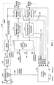
- Figure 1 is a block diagram that illustrates a system for power management of a universal asynchronous receiver/transmitter by automatic clock gating according to the present invention.
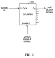
- Figure 2 is a schematic diagram that illustrates a synchronous clock gate and clock divide circuit employed within the system of Figure 1.
- FIG. 1 is a block diagram of one system for power management of a universal asynchronous receiver/transmitter by automatic clock gating according to the present invention.
- the system 100 includes a clock control unit 102, a synchronous clock gate 104, a clock divider unit 106, and a universal asynchronous receiver/transmitter (UART) circuit 108.
- the UART 108 includes a baud generator 110 coupled to a transmit state machine 112 and to a receiver state machine 114.
- a transmit FIFO and holding register 116 is coupled to transmit state machine 112, and a receiver FIFO and buffer register unit 118 is coupled to receiver state machine 114.
- a UART control logic unit 120 is finally coupled to baud generator 110, to transmit FIFO and holding register unit 116, and to receiver FIFO and buffer register unit 118.
- baud generator 110 receives a UART clock signal at line 122 and generates a baud rate signal at line 124 having a predetermined frequency.
- the baud rate signal is coupled to transmit state machine 112 and receiver state machine 114 and provides a timing reference to control the receipt and transmission of serial data.
- Parallel data may be provided from an external source to UART 108 via the CPU interface port 126.
- CPU interface port 126 may be connected to, for example, a CPU local bus or a peripheral bus.
- Parallel data provided to CPU interface port 126 is passed through UART control logic unit 120 and is stored within transmit FIFO and holding register 116.
- the parallel data is then transmitted in serial format by the transmit state machine 112 at the serial data output line 128.
- a shift register (not shown) is embodied within transmit state machine 112, and that techniques for achieving the conversion of the parallel data to serial data by transmit state machine 112 are well-known.
- Serial data is similarly received by the UART 108 at serial input line 130, and is converted to parallel data by receiver state machine 114.
- Each word of parallel data from receiver state machine 114 is provided to receiver FIFO and buffer register unit 118.
- the UART control logic unit 120 asserts an interrupt signal at line 132 that alerts the microprocessor of the availability of data within the receiver FIFO and buffer register unit 113.
- the microprocessor sequentially unloads the parallel data from the receiver FIFO and buffer register unit 118.
- An input clock signal Clock IN is provided to the synchronous clock gate 104 at line 136. If a clock enable control signal is asserted low at line 138, the Clock IN signal is provided to divider circuit 106 which correspondingly frequency divides the Clock IN signal to thereby derive the UART clock signal at line 122.
- the Clock IN signal at line 136 has a frequency of 24 Mhz
- the clock divider circuit 106 is a divide by 13 circuit. Accordingly, the UART clock signal at line 122 has a frequency of 1.8462 Mhz.
- the clock control unit 102 determines that the UART 108 is idle and is not currently receiving, processing or transmitting data, the clock enable signal at line 138 is deasserted high such that the Clock IN signal at line 136 is not provided to the clock divider circuit 106, and consequently such that the UART clock signal at line 122 is not generated.
- the baud rate signal at line 124 is not generated by baud generator 110. As a result, overall power consumption of the UART 108 is decreased when the UART is idle.
- the clock control unit 102 is provided to detect various predetermined system activities associated with UART 108 to determine whether the baud rate signal at line 124 must be generated. If the clock control unit determines that the baud rate signal must be generated, it asserts the clock enable signal which causes the synchronous clock gate to degate the Clock IN signal and thereby allows the baud rate signal to be generated. For the embodiment of Figure 1, the clock control unit 102 asserts the clock enable signal if any one of variety of system activities are detected. Specifically, the clock control unit monitors the transmit state machine 112, the receiver state machine 114, the transmit FIFO and holding register unit 116, and the receiver FIFO and buffer register unit 118 via lines 151-154. The clock control unit further monitors the serial input line 130.
- the clock enable signal at line 138 is asserted.
- These predetermined system activities are: the transmit state machine 112 is active, the receiver state machine 114 is active, the transmit FIFO and holding register unit 116 is not empty, the receiver FIFO and buffer register unit 118 is not empty, and a level transition is detected at the serial input line 130. Since each of these predetermined system activities indicates a need for the generation of the baud rate signal at line 124, the clock control unit asserts the clock enable signal upon detection.
- the clock control unit 102 deasserts the clock enable signal such that the Clock IN signal at line 136 is gated. As stated previously, when the Clock IN signal is gated, a baud rate signal is no longer generated at line 124, and power consumption is reduced.
- clock control unit 102 may also monitor other predetermined system activities to determine whether the baud rate signal must be generated. For example, in one configuration, the clock control unit monitors a system reset signal at line 160 and causes the clock enable signal to be asserted if an active reset is detected. The baud rate signal must be generated during this situation (when the reset signal is active) since the baud rate signal is necessary for initialization. Similarly, the clock control unit may be configured to detect certain system cycles at CPU interface port 126 if the baud rate signal is necessary to drive the UART control logic unit 120. Finally, the clock control unit may be configured to detect an active modem control signal at line 164 and to responsively assert the clock enable signal.
- the deassertion of the clock enable signal by the clock control unit 102 in response to the completion of a detected system activity may be delayed by a predetermined amount of time after the system activity completes or is no longer detected. Such a predetermined delay may be desirable to allow the UART 108 to complete operations associated with the detected activity.
- the clock control unit 102 asserts the clock enable signal when the reset signal becomes active. Subsequently, when the reset signal becomes inactive, the clock control unit 102 may be configured to wait a predetermined time before deasserting the clock enable signal. This may allow, for example, certain initialization operations to complete.
- FIG. 2 is a schematic diagram that illustrates an implementation of synchronous clock gate 104 and clock divider unit 106.
- a simple counter circuit 200 is employed to implement the synchronous clock gate 104 and clock divider unit 106 of Figure 1.
- An input clock signal is provided to a clock input of counter circuit 200, and a divided clock signal is extracted from one of the output lines of the counter circuit 200.
- the clock enable signal from clock control unit 102 is provided to an enable line of the counter circuit 200.
- the gating and degating of the Clock IN signal is performed synchronously with respect to the Clock IN signal, and clock "slivers" are thereby avoided.
- clock control unit 102 may be implemented with combinational logic circuitry, and that the clock control unit 102 may be enabled by an external enable signal. Furthermore, an empty flag associated with transmit FIFO and holding register 116 and an empty flag associated with receiver FIFO and buffer register 118 may be used to derive the monitored signals at lines 153 and 154.
- clock control unit 102 may monitor a time-out counter associated with receiver FIFO and buffer register unit 118.
- a time-out counter may be employed within a typical UART to cause an interrupt signal to be asserted to the microprocessor if data is held by the receiver FIFO 118 for a time duration that exceeds a time-out counter period.
- the clock control unit 102 asserts the clock enable signal during the time at which the time-out counter of receiver FIFO and buffer register 118 is active.
- the clock control unit 102 deasserts the clock enable signal such that the baud rate signal is no longer generated even if data is still contained within the receiver FIFO and buffer register unit 118.
- the microprocessor may unload the data from receiver FIFO and buffer register unit 118.
- the transmit FIFO and holding register unit 116 and the receiver FIFO and buffer register 118 may each be implemented using any type of data storage units.
- the transmit FIFO and holding register unit 116 as described above may include a multi-byte storage FIFO, or only a single-byte storage register.
- receiver FIFO and buffer register unit 113 may include a multi-byte storage FIFO, or only a single-byte storage register.
Abstract
Description
- This invention relates to asynchronous receiver/transmitter circuits, preferably to power management techniques employed within asynchronous receiver and transmitter circuits.
- A universal asynchronous receiver and transmitter, commonly abbreviated as a UART, is a prevalently employed communications element within computer systems that allows serial data transmission and reception. A major task of a UART is parallel-to-serial and serial-to-parallel conversion. Briefly speaking, a typical UART includes a pair of shift registers with associated FIFO buffers and control logic. Data to be serially transmitted is loaded into an output shift register, which is clocked at a predetermined bit rate. Start and stop bits are typically inserted that surround each data word during the serial data transmission. Serial data received by the UART is fed into an input shift register, and is clocked at the mid-point of each bit cell. The mid-point of each bit cell is determined by measuring the time relative to the start bit. When a complete word of data is received, the word is transferred into the FIFO buffer in parallel format. When the FIFO buffer is filled to a predetermined capacity, a microprocessor of the computer system is typically interrupted and the data is unloaded from the FIFO buffer.
- A typical UART further includes a variety of control and status registers that set and indicate various operating parameters, including the number of data bits, the number of stop bits, the type of parity, the clock divisor, and the status of the internal FIFO buffers. In addition to the basic serial input and output functions, most UART circuits also include connections for modem control handshake signals for RS-232 operation. Details regarding specific UART circuits may be found in a host of publications of the known prior art.
- One problem associated with typical UART circuits is that the serial input and output ports usually remain idle for a significant portion of time. During the idle condition of a UART, the receiver state machine which controls the receipt of serial input data is clocked by the internal baud rate generator even though data is not actually being received. The receiver state machine is continuously clocked since the times at which data will be received are usually not known ahead of time. In addition to the receiver state machine, the baud rate generator may also clock other portions of the UART circuit during the idle condition. As a result, power is wasted when the UART is idle since the baud rate signal is unnecessarily being generated and provided to various internal portions of the UART. This is a particular problem when UART circuits are employed within battery-powered portable computer systems.
- The problems outlined above are in large part solved by a system and technique for power management of a universal asynchronous receiver and transmitter by automatic clock gating to be described. In one embodiment, a clock control unit is provided that controls the gating of a clock signal received by an internal baud generator of a universal asynchronous receiver and transmitter (UART) circuit during an active mode. The clock control unit monitors the UART circuit to determine whether the UART is currently idle. If the clock control unit determines that the UART is idle, the clock signal is gated by a synchronous clock gate circuit. Accordingly, the clock signal is not provided to the baud generator, and a corresponding baud rate signal that normally clocks the receiver state machine of the UART is not generated. Power consumption of the UART is thereby significantly reduced. When a certain predetermined system activity is thereafter detected by the clock control unit that indicates a need for activation of the UART, the clock control unit asserts a clock enable signal that causes the synchronous clock gate circuit to pass the clock signal to an input of the baud generator. The baud generator responsively generates the baud rate signal that clocks the receiver state machine as well as other internal portions of the UART. In one embodiment, the clock control unit causes the clock signal to be degated if the receipt of serial data is detected at the serial input line of the UART (i.e., a falling edge of a start bit is detected), if the receiver state machine is currently active, if the receiver FIBO and buffer register is not empty, if the transmitter FIFO and holding register is not empty, or if the transmitter state machine is active. Depending upon the system, the clock control unit may further degate the clock signal if a level change is detected at a modem control line, if reset is active, or if a system cycle is in progress that involves the UART control logic. If none of these predetermined activities is detected by the clock control unit, the clock enable signal is deasserted and the synchronous clock gate circuit responsively gates the clock signal.
- Broadly speaking, a first aspect of the present invention contemplates a system comprising an asynchronous receiver and transmitter circuit including a baud generator for generating a baud rate signal, a receiver state machine coupled to the baud generator and capable of receiving serial data at a serial data input line, a transmit state machine coupled to the baud generator and capable of providing serial data at a serial data output line, a first data storage unit coupled to the receiver state machine for storing data received by the receiver state machine in a parallel format, and a second data storage unit coupled to the transmit state machine for storing data to be transmitted by the transmit state machine. A clock gate circuit is also provided having an input line for receiving an external clock signal and an output line for providing a UART clock signal to an input line of the baud generator, wherein the clock gate circuit selectively gates the external clock signal depending upon a clock enable signal. A clock control unit is coupled to the clock gate circuit and to the asynchronous receiver and transmitted circuit which is capable of detecting a predetermined system activity and is capable of asserting the clock enable signal if a predetermined system activity is detected.
- A second aspect of the present invention further contemplates a serial communications circuit comprising a baud generator for generating a baud rate signal, a receiver state machine coupled to the baud generator for receiving serial data at a serial data input line, and a transmit state machine coupled to the baud generator capable of providing serial data at a serial data output line. A first data storage unit is also provided that is coupled to the receiver state machine for storing data received by the receiver state machine in a parallel format. A second data storage unit is further coupled to the transmit state machine for storing data to be transmitted by the transmit state machine. A clock gate circuit having an input line for receiving an external clock input signal and an output line for providing a reference clock signal to the baud generator depending upon a clock enable signal is further provided. A clock control unit is finally provided coupled to the clock gate circuit, wherein the clock control unit is capable of detecting a predetermined system activity and is capable of asserting the clock enable signal if a predetermined system activity is detected.
- A third aspect of the present invention finally contemplates a power management method for an asynchronous receiver and transmitter circuit comprising the steps of providing a clock input signal to a clock gate circuit, detecting a predetermined system activity associated with the asynchronous receiver and transmitter, asserting a clock enable signal in response to the detection of a predetermined system activity, providing a clock enable signal to a control line of the clock gate signal to thereby provide a UART clock signal to a baud generator, and deasserting the clock enable signal in response to completion of a predetermined system activity.
- Other objects and advantages of the invention will become apparent upon reading the following detailed description and upon reference to the accompanying drawings in which:
- Figure 1 is a block diagram that illustrates a system for power management of a universal asynchronous receiver/transmitter by automatic clock gating according to the present invention.
- Figure 2 is a schematic diagram that illustrates a synchronous clock gate and clock divide circuit employed within the system of Figure 1.
- While the invention is susceptible to various modifications and alternative forms, preferred embodiments thereof are shown by way of example in the drawings and will herein be described in detail. It should be understood, however, that the drawings and detailed description thereto are not intended to limit the invention to the particular form disclosed, but on the contrary, the intention is to cover all modifications, equivalents and alternatives falling within the spirit and scope of the present invention as defined by the appended claims.
- Referring now to the drawings, Figure 1 is a block diagram of one system for power management of a universal asynchronous receiver/transmitter by automatic clock gating according to the present invention. The system 100 includes a
clock control unit 102, asynchronous clock gate 104, aclock divider unit 106, and a universal asynchronous receiver/transmitter (UART)circuit 108. The UART 108 includes abaud generator 110 coupled to a transmitstate machine 112 and to a receiver state machine 114. A transmit FIFO andholding register 116 is coupled to transmitstate machine 112, and a receiver FIFO andbuffer register unit 118 is coupled to receiver state machine 114. A UARTcontrol logic unit 120 is finally coupled tobaud generator 110, to transmit FIFO and holdingregister unit 116, and to receiver FIFO andbuffer register unit 118. - With respect to the transmission and receipt of serial data at
lines baud generator 110, transmitstate machine 112, receiver state machine 114, transmit FIFO andholding register 116, and receiver FIFO andbuffer register 118 are conventional. Similarly, with respect to the CPU interface atport 126, the design and operation of UARTcontrol logic unit 120 are also conventional. In the interest of simplicity and clarity, only a brief description regarding the conventional aspects of UART 108 will be provided below. - During normal operation,
baud generator 110 receives a UART clock signal atline 122 and generates a baud rate signal atline 124 having a predetermined frequency. The baud rate signal is coupled to transmitstate machine 112 and receiver state machine 114 and provides a timing reference to control the receipt and transmission of serial data. - Parallel data may be provided from an external source to UART 108 via the
CPU interface port 126.CPU interface port 126 may be connected to, for example, a CPU local bus or a peripheral bus. Parallel data provided toCPU interface port 126 is passed through UARTcontrol logic unit 120 and is stored within transmit FIFO andholding register 116. The parallel data is then transmitted in serial format by the transmitstate machine 112 at the serialdata output line 128. It is noted that a shift register (not shown) is embodied within transmitstate machine 112, and that techniques for achieving the conversion of the parallel data to serial data by transmitstate machine 112 are well-known. - Serial data is similarly received by the
UART 108 atserial input line 130, and is converted to parallel data by receiver state machine 114. Each word of parallel data from receiver state machine 114 is provided to receiver FIFO andbuffer register unit 118. When a certain predetermined number of words have been filled within receiver FIFO andbuffer register unit 118, or when, for example, a receiver time-out expires, the UARTcontrol logic unit 120 asserts an interrupt signal atline 132 that alerts the microprocessor of the availability of data within the receiver FIFO and buffer register unit 113. In response, the microprocessor sequentially unloads the parallel data from the receiver FIFO andbuffer register unit 118. - Details regarding the power management of UART 108 by automatic clock gating according to the present invention are next considered. An input clock signal Clock IN is provided to the
synchronous clock gate 104 atline 136. If a clock enable control signal is asserted low atline 138, the Clock IN signal is provided todivider circuit 106 which correspondingly frequency divides the Clock IN signal to thereby derive the UART clock signal atline 122. In one embodiment, the Clock IN signal atline 136 has a frequency of 24 Mhz, and theclock divider circuit 106 is a divide by 13 circuit. Accordingly, the UART clock signal atline 122 has a frequency of 1.8462 Mhz. - As will be understood better from the following description, if the
clock control unit 102 determines that theUART 108 is idle and is not currently receiving, processing or transmitting data, the clock enable signal atline 138 is deasserted high such that the Clock IN signal atline 136 is not provided to theclock divider circuit 106, and consequently such that the UART clock signal atline 122 is not generated. By removing the UART clock signal atline 122, the baud rate signal atline 124 is not generated bybaud generator 110. As a result, overall power consumption of theUART 108 is decreased when the UART is idle. - The
clock control unit 102 is provided to detect various predetermined system activities associated withUART 108 to determine whether the baud rate signal atline 124 must be generated. If the clock control unit determines that the baud rate signal must be generated, it asserts the clock enable signal which causes the synchronous clock gate to degate the Clock IN signal and thereby allows the baud rate signal to be generated. For the embodiment of Figure 1, theclock control unit 102 asserts the clock enable signal if any one of variety of system activities are detected. Specifically, the clock control unit monitors the transmitstate machine 112, the receiver state machine 114, the transmit FIFO and holdingregister unit 116, and the receiver FIFO andbuffer register unit 118 via lines 151-154. The clock control unit further monitors theserial input line 130. If any one of the following predetermined system activities are detected by theclock control unit 102, the clock enable signal atline 138 is asserted. These predetermined system activities are: the transmitstate machine 112 is active, the receiver state machine 114 is active, the transmit FIFO and holdingregister unit 116 is not empty, the receiver FIFO andbuffer register unit 118 is not empty, and a level transition is detected at theserial input line 130. Since each of these predetermined system activities indicates a need for the generation of the baud rate signal atline 124, the clock control unit asserts the clock enable signal upon detection. When the detected activity later completes and is no longer detected byclock control unit 102, and if none of the other predetermined system activities is currently being detected, theclock control unit 102 deasserts the clock enable signal such that the Clock IN signal atline 136 is gated. As stated previously, when the Clock IN signal is gated, a baud rate signal is no longer generated atline 124, and power consumption is reduced. - It is noted that depending upon the particular UART circuit, other predetermined system activities may also be monitored by
clock control unit 102 to determine whether the baud rate signal must be generated. For example, in one configuration, the clock control unit monitors a system reset signal atline 160 and causes the clock enable signal to be asserted if an active reset is detected. The baud rate signal must be generated during this situation (when the reset signal is active) since the baud rate signal is necessary for initialization. Similarly, the clock control unit may be configured to detect certain system cycles atCPU interface port 126 if the baud rate signal is necessary to drive the UARTcontrol logic unit 120. Finally, the clock control unit may be configured to detect an active modem control signal atline 164 and to responsively assert the clock enable signal. - It is further noted that the deassertion of the clock enable signal by the
clock control unit 102 in response to the completion of a detected system activity (as described above) may be delayed by a predetermined amount of time after the system activity completes or is no longer detected. Such a predetermined delay may be desirable to allow theUART 108 to complete operations associated with the detected activity. For example, as stated previously, theclock control unit 102 asserts the clock enable signal when the reset signal becomes active. Subsequently, when the reset signal becomes inactive, theclock control unit 102 may be configured to wait a predetermined time before deasserting the clock enable signal. This may allow, for example, certain initialization operations to complete. - Figure 2 is a schematic diagram that illustrates an implementation of
synchronous clock gate 104 andclock divider unit 106. As illustrated in Figure 2, asimple counter circuit 200 is employed to implement thesynchronous clock gate 104 andclock divider unit 106 of Figure 1. An input clock signal is provided to a clock input ofcounter circuit 200, and a divided clock signal is extracted from one of the output lines of thecounter circuit 200. The clock enable signal fromclock control unit 102 is provided to an enable line of thecounter circuit 200. In accordance with the synchronous clock gate and clock divider of Figure 2, the gating and degating of the Clock IN signal is performed synchronously with respect to the Clock IN signal, and clock "slivers" are thereby avoided. - Referring back to Figure 1, it is noted that
clock control unit 102 may be implemented with combinational logic circuitry, and that theclock control unit 102 may be enabled by an external enable signal. Furthermore, an empty flag associated with transmit FIFO and holdingregister 116 and an empty flag associated with receiver FIFO and buffer register 118 may be used to derive the monitored signals atlines - It is noted that in a further embodiment,
clock control unit 102 may monitor a time-out counter associated with receiver FIFO andbuffer register unit 118. As is known to those of skill in the art, such a time-out counter may be employed within a typical UART to cause an interrupt signal to be asserted to the microprocessor if data is held by thereceiver FIFO 118 for a time duration that exceeds a time-out counter period. For such an embodiment, theclock control unit 102 asserts the clock enable signal during the time at which the time-out counter of receiver FIFO andbuffer register 118 is active. When the count period of the time-out counter expires, theclock control unit 102 deasserts the clock enable signal such that the baud rate signal is no longer generated even if data is still contained within the receiver FIFO andbuffer register unit 118. Following the deassertion of the clock enable signal, the microprocessor may unload the data from receiver FIFO andbuffer register unit 118. - It is further noted that the transmit FIFO and holding
register unit 116 and the receiver FIFO and buffer register 118 may each be implemented using any type of data storage units. For example, the transmit FIFO and holdingregister unit 116 as described above may include a multi-byte storage FIFO, or only a single-byte storage register. Similarly, receiver FIFO and buffer register unit 113 may include a multi-byte storage FIFO, or only a single-byte storage register. - Numerous variations and modifications will become apparent to those skilled in the art once the above disclosure is fully appreciated. For example, the specific circuitry used to implement the internal subunits of
UART 108 may vary depending upon the requirements of a particular application. Furthermore, the predetermined system activities that are detected byclock control unit 102 may vary depending upon the particular UART circuit employed. In that regard, system activities in addition to those indicated above may be detected byclock control unit 102 and cause the clock enable signal to be asserted. It is intended that the following claims be interpreted to embrace all such variations and modifications.
Claims (20)
- A system comprising:
an asynchronous receiver and transmitter circuit including:
a baud generator for generating a baud rate signal;
a receiver state machine coupled to said baud generator and capable of receiving serial data at a serial data input line;
a transmit state machine coupled to said baud generator and capable of providing serial data at a serial data output line;
a first data storage unit coupled to said receiver state machine for storing data received by said receiver state machine in a parallel format; and
a second data storage unit coupled to said transmit state machine for storing data to be transmitted by said transmit state machine;
a clock gate circuit having an input line for receiving an external clock signal and an output line for providing a UART clock signal to an input line of said baud generator, wherein said clock gate circuit selectively gates said external clock signal depending upon a clock enable signal; and
a clock control unit coupled to said clock gate circuit and to said asynchronous receiver and transmitted circuit, wherein said clock control unit is capable of detecting a predetermined system activity and is capable of asserting said clock enable signal if said predetermined system activity is detected. - The system as recited in Claim 1 wherein said clock control unit is capable of detecting a signal transition at said serial data input line, and wherein said clock control unit asserts said clock enable signal in response to a detection of said signal transition at said serial data input line.
- The clock control unit as recited in Claim 1 wherein said clock control unit is coupled to said receiver state machine, wherein said clock control unit asserts said clock enable signal if said receiver state machine is active.
- The system as recited in Claim 1 wherein said clock control unit is coupled to said first data storage unit, wherein said clock control unit asserts said clock enable signal if said first data storage unit is not empty.
- The system as recited in Claim 1 wherein said asynchronous receiver and transmitter circuit further includes a control logic unit coupled to said first and second data storage units for interfacing data transfers between a microprocessor and said asynchronous receiver and transmitter.
- The system as recited in Claim 1 wherein said first data storage unit includes a FIFO buffer.
- The system as recited in Claim 1 further comprising a clock divider circuit connected between said clock gate circuit and said baud generator, wherein said clock gate circuit selectively provides said external clock signal to said divider circuit and wherein said divider circuit generates said UART clock signal.
- The system as recited in Claim 1 wherein said clock gate circuit is a synchronous clock gate circuit.
- The system as recited in Claim 7 wherein said clock gate circuit and said clock divider are implemented with a counter circuit.
- The system as recited in Claim 1 wherein said clock control unit is connected to said transmit state machine, and wherein said clock control unit asserts said clock enable signal if said transmit state machine is active.
- The system as recited in Claim 1 wherein said clock control unit deasserts said clock enable signal if said predetermined system activity is not detected.
- The system as recited in Claim 11 wherein said clock control unit deasserts said clock enable signal a predetermined time delay after said predetermined system activity completes.
- A serial communications circuit comprising:
a baud generator for generating a baud rate signal;
a receiver state machine coupled to said baud generator for receiving serial data at a serial data input line;
a transmit state machine coupled to said baud generator capable of providing serial data at a serial data output line;
a first data storage unit coupled to said receiver state machine for storing data received by said receiver state machine in a parallel format;
a second data storage unit coupled to said transmit state machine for storing data to be transmitted by said transmit state machine;
a clock gate circuit having an input line for receiving an external clock input signal and an output line for providing a reference clock signal to said baud generator, wherein said clock gate circuit selectively gates said external clock signal depending upon a clock enable signal; and
a clock control unit coupled to said clock gate circuit, wherein said clock control unit is capable or detecting a predetermined system activity and is capable of asserting said clock enable signal if said predetermined system activity is detected. - The serial communications circuit as recited in Claim 13 wherein said clock control unit is capable of detecting a signal transition at said serial data input line, and wherein said clock control unit asserts said clock enable signal in response to a detection of a signal transition at said serial data input line.
- The serial communications circuit as recited in Claim 13 wherein said clock control unit is coupled to said receiver state machine, wherein said clock control unit asserts said clock enable signal if said receiver state machine is active.
- The serial communications circuit as recited in Claim 13 wherein said clock control unit deasserts said clock enable signal if said predetermined system activity is not detected.
- The serial communications circuit as recited in Claim 13 wherein said clock control unit deasserts said clock enable signal a predetermined time delay after said predetermined system activity completes.
- A power management method for an asynchronous receiver and transmitter circuit comprising the steps of:
providing a clock input signal to a clock gate circuit;
detecting a predetermined system activity associated with said asynchronous receiver and transmitter;
asserting a clock enable signal in response to the detection of said predetermined system activity;
providing said clock enable signal to a control line of said clock gate signal to thereby provide a UART clock signal to a baud generator; and
deasserting said clock enable signal in response to completion of said predetermined system activity. - The method for managing power within an asynchronous receiver and transmitter circuit wherein said step of detecting a predetermined system activity includes the step of detecting whether a receiver state machine is receiving serial data at a serial data input line.
- The method for managing power within an asynchronous receiver and transmitter circuit comprising the further steps of:
detecting whether a receiver storage unit contains data; and
asserting said clock enable signal if said receiver storage unit contains data.
Applications Claiming Priority (2)
| Application Number | Priority Date | Filing Date | Title |
|---|---|---|---|
| US19138894A | 1994-02-02 | 1994-02-02 | |
| US191388 | 1994-02-02 |
Publications (2)
| Publication Number | Publication Date |
|---|---|
| EP0666529A1 true EP0666529A1 (en) | 1995-08-09 |
| EP0666529B1 EP0666529B1 (en) | 2004-10-06 |
Family
ID=22705293
Family Applications (1)
| Application Number | Title | Priority Date | Filing Date |
|---|---|---|---|
| EP95300444A Expired - Lifetime EP0666529B1 (en) | 1994-02-02 | 1995-01-25 | Power management in an asynchronus receiver/transmitter |
Country Status (5)
| Country | Link |
|---|---|
| US (1) | US5661751A (en) |
| EP (1) | EP0666529B1 (en) |
| JP (1) | JP3570762B2 (en) |
| AT (1) | ATE278984T1 (en) |
| DE (1) | DE69533599T2 (en) |
Cited By (8)
| Publication number | Priority date | Publication date | Assignee | Title |
|---|---|---|---|---|
| WO1997042730A1 (en) * | 1996-05-08 | 1997-11-13 | Ericsson Inc. | Half duplex uart control for single channel bi-directional wireless communications |
| US5713028A (en) * | 1995-01-30 | 1998-01-27 | Fujitsu Limited | Micro-processor unit having universal asynchronous receiver/transmitter |
| GB2349722A (en) * | 1999-01-19 | 2000-11-08 | Ibm | Power supply controller for computer peripheral device |
| WO2003021453A2 (en) * | 2001-08-29 | 2003-03-13 | Analog Devices, Inc. | Generic serial port architecture and system |
| FR2830956A1 (en) * | 2001-10-15 | 2003-04-18 | St Microelectronics Sa | Asynchronous receiver, especially a UART, for use in a microcontroller has an improved circuit design that enables faster changeover from standby mode to operating mode |
| FR2845176A1 (en) * | 2002-03-22 | 2004-04-02 | Zarlink Semiconductor Ltd | DATA EXCHANGE PROCESS |
| DE10159247B4 (en) * | 2000-12-11 | 2005-01-05 | Visteon Global Technologies, Inc., Dearborn | Apparatus and method for performing power management of automotive multimedia systems |
| KR100582112B1 (en) * | 1996-05-08 | 2006-09-11 | 에릭슨 인크. | Half-duplex UART controller for single channel bidirectional wireless communication |
Families Citing this family (31)
| Publication number | Priority date | Publication date | Assignee | Title |
|---|---|---|---|---|
| US5787115A (en) * | 1995-12-28 | 1998-07-28 | Northern Telecom Limited | Key telephone system without common control |
| US5903601A (en) * | 1996-12-17 | 1999-05-11 | Texas Instruments Incorporated | Power reduction for UART applications in standby mode |
| TW455805B (en) * | 1998-02-26 | 2001-09-21 | Winbond Electronics Corp | Converter allowing data communications equipment to transmit data to data terminal equipment through universal serial bus and the control method thereof |
| US6097243A (en) * | 1998-07-21 | 2000-08-01 | International Business Machines Corporation | Device and method to reduce power consumption in integrated semiconductor devices using a low power groggy mode |
| US6378026B1 (en) * | 1998-11-09 | 2002-04-23 | Sipex Corporation | Connection detection circuit and method |
| JP3565730B2 (en) * | 1999-01-13 | 2004-09-15 | 株式会社リコー | AT command analyzer |
| JP3266127B2 (en) * | 1999-01-25 | 2002-03-18 | 日本電気株式会社 | Synchronous semiconductor memory device |
| US6232820B1 (en) * | 1999-06-14 | 2001-05-15 | Intel Corporation | Method and apparatus for dynamic clock gating |
| US6377071B1 (en) * | 2000-03-31 | 2002-04-23 | Cypress Semiconductor Corp. | Composite flag generation for DDR FIFOs |
| US6675305B1 (en) * | 2000-08-04 | 2004-01-06 | Synopsys, Inc. | Power saving in a USB peripheral by providing gated clock signal to CSR block in response to a local interrupt generated when an operation is to be performed |
| US6895518B2 (en) * | 2001-05-31 | 2005-05-17 | Koninklijke Philips Electronics N.V. | Power and frequency adjustable UART device |
| JP3749211B2 (en) * | 2002-09-06 | 2006-02-22 | 株式会社東芝 | Serial data receiving circuit |
| US6809570B2 (en) * | 2003-01-21 | 2004-10-26 | Hewlett-Packard Development Company, L.P. | Clock gater circuit |
| US20050198542A1 (en) * | 2004-03-08 | 2005-09-08 | David Freker | Method and apparatus for a variable memory enable deassertion wait time |
| EP1785982A1 (en) * | 2005-11-14 | 2007-05-16 | Texas Instruments Incorporated | Display power management |
| EP1785810A1 (en) * | 2005-11-14 | 2007-05-16 | Texas Instruments Incorporated | Idle mode for power mangagement |
| EP1785809A1 (en) * | 2005-11-14 | 2007-05-16 | Texas Instruments Inc. | Standby mode for power management |
| US8458429B2 (en) * | 2006-12-31 | 2013-06-04 | Texas Instruments Incorporated | Memory controller idle mode |
| US7667549B2 (en) | 2007-04-26 | 2010-02-23 | Semiconductor Energy Laboratory Co., Ltd. | Semiconductor device and driving method thereof |
| CN101453315B (en) * | 2007-12-05 | 2011-06-22 | 中兴通讯股份有限公司 | Data transmission method for time clock tracking data |
| KR101770981B1 (en) | 2009-10-30 | 2017-08-24 | 가부시키가이샤 한도오따이 에네루기 켄큐쇼 | Logic circuit and semiconductor device |
| WO2011065208A1 (en) | 2009-11-27 | 2011-06-03 | Semiconductor Energy Laboratory Co., Ltd. | Semiconductor device and method for manufacturing the same |
| KR102467172B1 (en) * | 2016-01-25 | 2022-11-14 | 삼성전자주식회사 | Semiconductor device |
| DE102017110821A1 (en) | 2016-01-25 | 2018-07-26 | Samsung Electronics Co., Ltd. | Semiconductor device |
| US10209734B2 (en) | 2016-01-25 | 2019-02-19 | Samsung Electronics Co., Ltd. | Semiconductor device, semiconductor system, and method of operating the semiconductor device |
| US10303203B2 (en) | 2016-01-25 | 2019-05-28 | Samsung Electronics Co., Ltd. | Semiconductor device, semiconductor system and method for operating semiconductor device |
| US10296066B2 (en) | 2016-01-25 | 2019-05-21 | Samsung Electronics Co., Ltd. | Semiconductor device, semiconductor system, and method of operating the semiconductor device |
| US10248155B2 (en) | 2016-01-25 | 2019-04-02 | Samsung Electronics Co., Ltd. | Semiconductor device including clock generating circuit and channel management circuit |
| TWI693498B (en) * | 2019-04-17 | 2020-05-11 | 方可成 | Multi-bit optical computing system |
| CN113448907B (en) * | 2021-08-31 | 2021-12-21 | 北京智联安科技有限公司 | Low-power-consumption serial asynchronous transceiver, data receiving method and medium |
| KR102454640B1 (en) * | 2022-01-04 | 2022-10-14 | (주)파인디어칩 | Integrated circuit having adaptive uart serial interface |
Citations (5)
| Publication number | Priority date | Publication date | Assignee | Title |
|---|---|---|---|---|
| US4665328A (en) * | 1984-07-27 | 1987-05-12 | National Semiconductor Corporation | Multiple clock power down method and structure |
| US4841440A (en) * | 1983-04-26 | 1989-06-20 | Nec Corporation | Control processor for controlling a peripheral unit |
| WO1991000566A1 (en) * | 1989-06-30 | 1991-01-10 | Poqet Computer Corporation | Computer power management system |
| EP0446519A2 (en) * | 1990-03-13 | 1991-09-18 | Mitsubishi Denki Kabushiki Kaisha | Noncontact integrated circuit card |
| EP0569131A2 (en) * | 1992-04-07 | 1993-11-10 | Mitsubishi Denki Kabushiki Kaisha | IC card |
Family Cites Families (10)
| Publication number | Priority date | Publication date | Assignee | Title |
|---|---|---|---|---|
| US4381552A (en) * | 1978-12-08 | 1983-04-26 | Motorola Inc. | Stanby mode controller utilizing microprocessor |
| US4851987A (en) * | 1986-01-17 | 1989-07-25 | International Business Machines Corporation | System for reducing processor power consumption by stopping processor clock supply if a desired event does not occur |
| US4835737A (en) * | 1986-07-21 | 1989-05-30 | American Telephone And Telegraph Company, At&T Bell Laboratories | Method and apparatus for controlled removal and insertion of circuit modules |
| US4878196A (en) * | 1986-12-18 | 1989-10-31 | Rose Frederick A | Communications management system |
| US4949333A (en) * | 1987-04-02 | 1990-08-14 | Advanced Micro Devices, Inc. | Enhanced universal asynchronous receiver-transmitter |
| US5167024A (en) * | 1989-09-08 | 1992-11-24 | Apple Computer, Inc. | Power management for a laptop computer with slow and sleep modes |
| US5237692A (en) * | 1990-11-09 | 1993-08-17 | Ast Research Inc. | Internal interrupt controller for a peripheral controller |
| EP0584257B1 (en) * | 1991-05-17 | 2004-08-04 | Packard Bell NEC, Inc. | Power management capability for a microprocessor having backward compatibility |
| JP2738229B2 (en) * | 1992-08-03 | 1998-04-08 | 日本電気株式会社 | Serial data communication controller |
| US5337285A (en) * | 1993-05-21 | 1994-08-09 | Rambus, Inc. | Method and apparatus for power control in devices |
-
1995
- 1995-01-25 EP EP95300444A patent/EP0666529B1/en not_active Expired - Lifetime
- 1995-01-25 DE DE69533599T patent/DE69533599T2/en not_active Expired - Lifetime
- 1995-01-25 AT AT95300444T patent/ATE278984T1/en not_active IP Right Cessation
- 1995-01-26 JP JP01065995A patent/JP3570762B2/en not_active Expired - Fee Related
-
1996
- 1996-02-15 US US08/602,261 patent/US5661751A/en not_active Expired - Lifetime
Patent Citations (5)
| Publication number | Priority date | Publication date | Assignee | Title |
|---|---|---|---|---|
| US4841440A (en) * | 1983-04-26 | 1989-06-20 | Nec Corporation | Control processor for controlling a peripheral unit |
| US4665328A (en) * | 1984-07-27 | 1987-05-12 | National Semiconductor Corporation | Multiple clock power down method and structure |
| WO1991000566A1 (en) * | 1989-06-30 | 1991-01-10 | Poqet Computer Corporation | Computer power management system |
| EP0446519A2 (en) * | 1990-03-13 | 1991-09-18 | Mitsubishi Denki Kabushiki Kaisha | Noncontact integrated circuit card |
| EP0569131A2 (en) * | 1992-04-07 | 1993-11-10 | Mitsubishi Denki Kabushiki Kaisha | IC card |
Cited By (18)
| Publication number | Priority date | Publication date | Assignee | Title |
|---|---|---|---|---|
| US5713028A (en) * | 1995-01-30 | 1998-01-27 | Fujitsu Limited | Micro-processor unit having universal asynchronous receiver/transmitter |
| USRE40346E1 (en) * | 1996-05-08 | 2008-05-27 | Telefonaktiebolaget Lm Ericsson (Publ) | Method and apparatus for providing single channel communications |
| US5918024A (en) * | 1996-05-08 | 1999-06-29 | Ericsson, Inc. | Method and apparatus for providing single channel communications |
| AU724162B2 (en) * | 1996-05-08 | 2000-09-14 | Ericsson Inc. | Half duplex UART control for single channel bi-directional wireless communications |
| KR100582112B1 (en) * | 1996-05-08 | 2006-09-11 | 에릭슨 인크. | Half-duplex UART controller for single channel bidirectional wireless communication |
| WO1997042730A1 (en) * | 1996-05-08 | 1997-11-13 | Ericsson Inc. | Half duplex uart control for single channel bi-directional wireless communications |
| GB2349722B (en) * | 1999-01-19 | 2003-07-23 | Ibm | Computer power supply controller |
| US6317839B1 (en) | 1999-01-19 | 2001-11-13 | International Business Machines Corporation | Method of and apparatus for controlling supply of power to a peripheral device in a computer system |
| GB2349722A (en) * | 1999-01-19 | 2000-11-08 | Ibm | Power supply controller for computer peripheral device |
| DE10159247B4 (en) * | 2000-12-11 | 2005-01-05 | Visteon Global Technologies, Inc., Dearborn | Apparatus and method for performing power management of automotive multimedia systems |
| WO2003021453A2 (en) * | 2001-08-29 | 2003-03-13 | Analog Devices, Inc. | Generic serial port architecture and system |
| CN100361109C (en) * | 2001-08-29 | 2008-01-09 | 模拟设备公司 | Generic serial port architecture and system |
| WO2003021453A3 (en) * | 2001-08-29 | 2004-03-18 | Analog Devices Inc | Generic serial port architecture and system |
| US7114093B2 (en) | 2001-08-29 | 2006-09-26 | Analog Devices, Inc. | Generic architecture and system for a programmable serial port having a shift register and state machine therein |
| WO2003034247A2 (en) * | 2001-10-15 | 2003-04-24 | Stmicroelectronics Sa | Asynchronous data receiver comprising means for standby mode switchover |
| WO2003034247A3 (en) * | 2001-10-15 | 2003-09-25 | St Microelectronics Sa | Asynchronous data receiver comprising means for standby mode switchover |
| FR2830956A1 (en) * | 2001-10-15 | 2003-04-18 | St Microelectronics Sa | Asynchronous receiver, especially a UART, for use in a microcontroller has an improved circuit design that enables faster changeover from standby mode to operating mode |
| FR2845176A1 (en) * | 2002-03-22 | 2004-04-02 | Zarlink Semiconductor Ltd | DATA EXCHANGE PROCESS |
Also Published As
| Publication number | Publication date |
|---|---|
| ATE278984T1 (en) | 2004-10-15 |
| US5661751A (en) | 1997-08-26 |
| DE69533599T2 (en) | 2005-10-13 |
| JP3570762B2 (en) | 2004-09-29 |
| JPH07307765A (en) | 1995-11-21 |
| DE69533599D1 (en) | 2004-11-11 |
| EP0666529B1 (en) | 2004-10-06 |
Similar Documents
| Publication | Publication Date | Title |
|---|---|---|
| US5661751A (en) | System and technique for power management of a universal asynchronous receiver/transmitter by automatic clock gating | |
| KR100819720B1 (en) | Data processing system having an on-chip background debug system and method therefor | |
| US5493684A (en) | Power management architecture including a power management messaging bus for conveying an encoded activity signal for optimal flexibility | |
| US5996083A (en) | Microprocessor having software controllable power consumption | |
| EP1214662B1 (en) | System and method for initiating a serial data transfer between two clock domains | |
| US6108729A (en) | Serial bus system for shadowing registers | |
| US6546496B1 (en) | Network interface with power conservation using dynamic clock control | |
| US20100115311A1 (en) | PCI Express System and Method of Transiting Link State Thereof | |
| JP6074052B2 (en) | Virtual GPIO | |
| EP0665502A1 (en) | Asynchronous serial control circuit | |
| US6167078A (en) | Conservation of power in a serial modem | |
| JP6538715B2 (en) | Hybrid virtual GPIO | |
| US5640573A (en) | Power management message bus for integrated processor | |
| US5701514A (en) | System providing user definable selection of different data transmission modes of drivers of an I/O controller transmitting to peripherals with different data transmission rate | |
| JPH08263466A (en) | Integrated processor,integrated computer system and computersystem | |
| JPH08180013A (en) | Computer system,method for reconfiguration of configuration register of pci bus device in response to change in pci bus clock signal frequency and method in which pci bus interfacenotifies operator of operating speed different from pci bus | |
| JPH0844464A (en) | Computer system | |
| US6304911B1 (en) | Information packet reception indicator for reducing the utilization of a host system processor unit | |
| EP0770952A1 (en) | Power management in an information processing system | |
| EP1472609B1 (en) | Low-power bus interface | |
| EP0834105B1 (en) | Wake-up system for a pcmcia card | |
| US5461701A (en) | System and method for peripheral data transfer | |
| US5586123A (en) | Interface and loopback circuit for character based computer peripheral devices | |
| US7197578B1 (en) | Power management system for bridge circuit | |
| JP2000183894A (en) | Transmission controller |
Legal Events
| Date | Code | Title | Description |
|---|---|---|---|
| PUAI | Public reference made under article 153(3) epc to a published international application that has entered the european phase |
Free format text: ORIGINAL CODE: 0009012 |
|
| AK | Designated contracting states |
Kind code of ref document: A1 Designated state(s): AT BE DE DK ES FR GB GR IE IT LU NL PT SE |
|
| 17P | Request for examination filed |
Effective date: 19951113 |
|
| 17Q | First examination report despatched |
Effective date: 20021010 |
|
| GRAP | Despatch of communication of intention to grant a patent |
Free format text: ORIGINAL CODE: EPIDOSNIGR1 |
|
| GRAS | Grant fee paid |
Free format text: ORIGINAL CODE: EPIDOSNIGR3 |
|
| GRAA | (expected) grant |
Free format text: ORIGINAL CODE: 0009210 |
|
| AK | Designated contracting states |
Kind code of ref document: B1 Designated state(s): AT BE DE DK ES FR GB GR IE IT LU NL PT SE |
|
| PG25 | Lapsed in a contracting state [announced via postgrant information from national office to epo] |
Ref country code: NL Free format text: LAPSE BECAUSE OF FAILURE TO SUBMIT A TRANSLATION OF THE DESCRIPTION OR TO PAY THE FEE WITHIN THE PRESCRIBED TIME-LIMIT Effective date: 20041006 Ref country code: IT Free format text: LAPSE BECAUSE OF FAILURE TO SUBMIT A TRANSLATION OF THE DESCRIPTION OR TO PAY THE FEE WITHIN THE PRESCRIBED TIME-LIMIT;WARNING: LAPSES OF ITALIAN PATENTS WITH EFFECTIVE DATE BEFORE 2007 MAY HAVE OCCURRED AT ANY TIME BEFORE 2007. THE CORRECT EFFECTIVE DATE MAY BE DIFFERENT FROM THE ONE RECORDED. Effective date: 20041006 Ref country code: BE Free format text: LAPSE BECAUSE OF FAILURE TO SUBMIT A TRANSLATION OF THE DESCRIPTION OR TO PAY THE FEE WITHIN THE PRESCRIBED TIME-LIMIT Effective date: 20041006 Ref country code: AT Free format text: LAPSE BECAUSE OF FAILURE TO SUBMIT A TRANSLATION OF THE DESCRIPTION OR TO PAY THE FEE WITHIN THE PRESCRIBED TIME-LIMIT Effective date: 20041006 |
|
| REG | Reference to a national code |
Ref country code: GB Ref legal event code: FG4D |
|
| REG | Reference to a national code |
Ref country code: IE Ref legal event code: FG4D |
|
| REF | Corresponds to: |
Ref document number: 69533599 Country of ref document: DE Date of ref document: 20041111 Kind code of ref document: P |
|
| PG25 | Lapsed in a contracting state [announced via postgrant information from national office to epo] |
Ref country code: SE Free format text: LAPSE BECAUSE OF FAILURE TO SUBMIT A TRANSLATION OF THE DESCRIPTION OR TO PAY THE FEE WITHIN THE PRESCRIBED TIME-LIMIT Effective date: 20050106 Ref country code: GR Free format text: LAPSE BECAUSE OF FAILURE TO SUBMIT A TRANSLATION OF THE DESCRIPTION OR TO PAY THE FEE WITHIN THE PRESCRIBED TIME-LIMIT Effective date: 20050106 Ref country code: DK Free format text: LAPSE BECAUSE OF FAILURE TO SUBMIT A TRANSLATION OF THE DESCRIPTION OR TO PAY THE FEE WITHIN THE PRESCRIBED TIME-LIMIT Effective date: 20050106 |
|
| PG25 | Lapsed in a contracting state [announced via postgrant information from national office to epo] |
Ref country code: ES Free format text: LAPSE BECAUSE OF FAILURE TO SUBMIT A TRANSLATION OF THE DESCRIPTION OR TO PAY THE FEE WITHIN THE PRESCRIBED TIME-LIMIT Effective date: 20050117 |
|
| PG25 | Lapsed in a contracting state [announced via postgrant information from national office to epo] |
Ref country code: LU Free format text: LAPSE BECAUSE OF NON-PAYMENT OF DUE FEES Effective date: 20050125 Ref country code: IE Free format text: LAPSE BECAUSE OF NON-PAYMENT OF DUE FEES Effective date: 20050125 |
|
| NLV1 | Nl: lapsed or annulled due to failure to fulfill the requirements of art. 29p and 29m of the patents act | ||
| PLBE | No opposition filed within time limit |
Free format text: ORIGINAL CODE: 0009261 |
|
| STAA | Information on the status of an ep patent application or granted ep patent |
Free format text: STATUS: NO OPPOSITION FILED WITHIN TIME LIMIT |
|
| ET | Fr: translation filed | ||
| 26N | No opposition filed |
Effective date: 20050707 |
|
| REG | Reference to a national code |
Ref country code: IE Ref legal event code: MM4A |
|
| PG25 | Lapsed in a contracting state [announced via postgrant information from national office to epo] |
Ref country code: PT Free format text: LAPSE BECAUSE OF NON-PAYMENT OF DUE FEES Effective date: 20050306 |
|
| REG | Reference to a national code |
Ref country code: GB Ref legal event code: 732E Free format text: REGISTERED BETWEEN 20091126 AND 20091202 |
|
| REG | Reference to a national code |
Ref country code: FR Ref legal event code: TP |
|
| PGFP | Annual fee paid to national office [announced via postgrant information from national office to epo] |
Ref country code: FR Payment date: 20101221 Year of fee payment: 17 |
|
| PGFP | Annual fee paid to national office [announced via postgrant information from national office to epo] |
Ref country code: GB Payment date: 20101215 Year of fee payment: 17 |
|
| PGFP | Annual fee paid to national office [announced via postgrant information from national office to epo] |
Ref country code: DE Payment date: 20110131 Year of fee payment: 17 |
|
| GBPC | Gb: european patent ceased through non-payment of renewal fee |
Effective date: 20120125 |
|
| REG | Reference to a national code |
Ref country code: FR Ref legal event code: ST Effective date: 20120928 |
|
| PG25 | Lapsed in a contracting state [announced via postgrant information from national office to epo] |
Ref country code: DE Free format text: LAPSE BECAUSE OF NON-PAYMENT OF DUE FEES Effective date: 20120801 Ref country code: GB Free format text: LAPSE BECAUSE OF NON-PAYMENT OF DUE FEES Effective date: 20120125 |
|
| REG | Reference to a national code |
Ref country code: DE Ref legal event code: R119 Ref document number: 69533599 Country of ref document: DE Effective date: 20120801 |
|
| PG25 | Lapsed in a contracting state [announced via postgrant information from national office to epo] |
Ref country code: FR Free format text: LAPSE BECAUSE OF NON-PAYMENT OF DUE FEES Effective date: 20120131 |