BACKGROUND OF THE INVENTION
Field Of The Invention
This invention relates to computer systems and, more particularly, to methods and
apparatus for providing a frame buffer capable of receiving, manipulating and
transferring data for display at a high rate of speed when used in a system
displaying a plurality of applications simultaneously in windows on an output
display device.
History Of The Prior Art
One of the significant problems involved in increasing the ability of desktop
computers has been in finding ways to increase the rate at which information is
transferred to an output display device. The various forms of data presentation
which are presently available require that copious amounts of data be transferred.
For example, if a computer output display monitor is operating in a color mode in
which 1024 X 780 pixels are displayed on the screen and the mode is one in which
thirty-two bits are used to define each pixel, then a total of over twenty-five
millions bits of information must be transferred to the screen with each frame that is
displayed. Typically, sixty frames are displayed each second so that over one and
one-half billion bits must be transferred each second. This requires a very
substantial amount of processing power. In general, the transfer of this data to the
display slows the overall operation of the computer.
In order to speed the process of transferring data to the display, various accelerating
circuitry has been devised. This circuitry is adapted to relieve the central processor
of the computer of the need to accomplish many of the functions necessary to the
transfer of data to the display. Essentially, these accelerators take over various
operations which the central processor would normally be required to accomplish.
For example, block transfers of data from one position on the screen to another
require that each line of data on the screen being transferred be read and rewritten to
a new line. Storing information within window areas of a display requires that data
available for each window portion be clipped to fit within that window portion and
not overwrite other portions of the display. Many other functions require the
generation of various vectors when an image within a window on the display is cleared or
moved. All of these operations require a substantial portion of the time available to a central
processing unit. These repetitive sorts of functions may be accomplished by a graphic
accelerator and relieve the central processor of the burden. In general, it has been found that
if operations which handle a great number of pixels at once are mechanized by a graphics
accelerator, then the greatest increase in display speed may be attained. This, of course,
speeds the operations involved in graphical display.
A problem which has been discovered by designers of graphics accelerator circuitry is
that a great deal of the speed improvement which is accomplished by the graphics accelerator
circuitry is negated by the frame buffer circuitry into which the output of the graphics
accelerator is loaded for ultimate display on an output display device. Typically, a frame
buffer offers a sufficient amount of random access memory to store one frame of data to be
displayed. However, transferring the data to and from the frame buffer is very slow because
of the manner in which the frame buffers are constructed. Various improvements have been
made to speed access in frame buffers. For example, two-ported VRAM has been substituted
for DRAM so that information may be taken from the frame buffer while it is being loaded.
A flash mode has been devised for allowing an entire row of a display to be written with a
single color. This mode is useful when the entire display is being cleared but cannot provide
clipping to limited areas and so is not useful when windows are displayed on the screen of an
output display. Since the design of prior art frame buffers has produced a substantial bottle
neck to rapid display of data in modem windowing systems, a new design of frame buffers
allowing substantially increased display speed is desirable.
Examples of prior art arrangements are disclosed in EP-A-0225,197 (Digital
Equipment Corporation), US-A-4,807,189 (Pinkham et al) and US-A-5,046,023 (Hitachi Ltd).
Summary Of The Invention
It is, therefore, an object of the present invention to provide a new design of frame
buffer capable of rapidly handling the data transferred to it for display in a system which
presents a plurality of applications in separate windows on an output display device.
It is another more specific object of the present invention to provide a new design of
frame buffer capable of speeding the display of data by factors which are the order the
magnitude of the prior art frame buffers.
These and other objects and features of the invention will be better understood by
reference to the detailed description which follows taken together with the drawings
in which like elements are referred to by like designations throughout the several
views.
Brief Description Of The Drawings
Figure 1 is a block diagram illustrating a computer system including the present
invention.
Figure 2 is a block diagram of a frame buffer designed in accordance with prior art.
Figure 3 is a block diagram of a frame buffer designed in accordance with the
present invention.
Figure 4 is a diagram illustrating operational details of a portion of the frame buffer
of Figure 3.
Figure 5 is a flow chart illustrating a method in accordance with the invention.
Notation And Nomenclature
Some portions of the detailed descriptions which follow are presented in terms of
symbolic representations of operations on data bits within a computer memory.
These descriptions and representations are the means used by those skilled in the
data processing arts to most effectively convey the substance of their work to others
skilled in the art. The operations are those requiring physical manipulations of
physical quantities. Usually, though not necessarily, these quantities take the form
of electrical or magnetic signals capable of being stored, transferred, combined,
compared, and otherwise manipulated. It has proven convenient at times,
principally for reasons of common usage, to refer to these signals as bits, values,
elements, symbols, characters, terms, numbers, or the like. It should be borne in
mind, however, that all of these and similar terms are to be associated with the
appropriate physical quantities and are merely convenient labels applied to these
quantities.
Further, the manipulations performed are often referred to in terms, such as adding
or comparing, which are commonly associated with mental operations performed
by a human operator. No such capability of a human operator is necessary or
desirable in most cases in any of the operations described herein which form part of
the present invention; the operations are machine operations. Useful machines for
performing the operations of the present invention include general purpose digital
computers or other similar devices. In all cases the distinction between the method
operations in operating a computer and the method of computation itself should be
borne in mind. The present invention relates to a method and apparatus for
operating a computer in processing electrical or other (e.g. mechanical, chemical)
physical signals to generate other desired physical signals.
Detailed Description Of The Invention
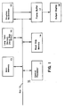
Referring now to Figure 1, there is illustrated a computer system 10. The system
10 includes a central processor 11 which carries out the various instructions
provided to the computer 10 for its operations. The central processor 11 is joined
to a bus 12 adapted to carry information to various components of the system 10.
Joined to the bus 12 is main memory 13 which is typically constructed of dynamic
random access memory arranged in a manner well known to those skilled in the
prior art to store information being used by the central processor during the period
in which power is provided to the system 10. Also joined to the bus 12 is read
only memory 14 which may include various memory devices (such as electrically
programmable read only memory devices (EPROM or similar devices)) well known
to those skilled in the art which are adapted to retain memory condition in the
absence of power to the system 10. The read only memory 14 typically stores
various basic functions used by the processor 11 such as basic input/output
processes and startup processes.
Also connected to the bus 12 are various peripheral components such as long term
memory 16. The construction and operation of long term memory 16 (typically
electro-mechanical hard disk drives) are well known to those skilled in the art.
Also joined to the bus 12 is circuitry such as a frame buffer 17 to which data may
be written that is to be transferred to an output device such as a monitor 18 for
display. For the purposes of the present explanation, the frame buffer may be
considered to include in addition to the various memory planes necessary to store
information, various circuitry well known to those skilled in the art for controlling
the scan of information to the output display.
Figure 2 illustrates a frame buffer 17 constructed in accordance with the prior art.
Typically, such a frame buffer 17 includes a dynamic random access memory array
designed to store information defining pixels on the output display. When the
random access memory of a frame buffer 17 is accessed in its normal mode of
operation, data is written to or read from the frame buffer 17 on the conductors of
the data bus 12. When the frame buffer 17 is written, all of the data conductors of
the bus transfer the binary data to be stored as pixel information. In a typical
computer system having a thirty-two bit bus, thirty-two bits of information may be
written on the bus and appear at thirty-two input pins to the frame buffer memory.
This data may define one or more pixels depending upon the number of bits
required to define a pixel in the particular display mode. For example, in an eight
bit color mode of operation, each pixel displayed requires eight bits of data; and
thirty-two bits of data on the data conductors of the bus are capable of defining four
pixels in each individual access. Writing pixel data one (or four) pixels at a time is
a relatively slow method of filling the frame buffer with data to be written to the
display. This is, however, the usual mode of writing pixel data to the display.
This normal mode is typically used in any process which varies the display on a
pixel by pixel basis or to describe any graphical image which uses more than two
colors in a window.
There are many operations which affect the display, however, which manipulate
very large numbers of pixels and do not require that pixels be individually varied.
These operations include, for example, clearing the entire display or a window of
the display and similar operations. Because filling the frame buffer is so slow
when each pixel is individually described on the data conductors, some prior art
frame buffers also have apparatus which allows a mode of operation (referred to as
"block mode") in which each of the data conductors controls access to four bits
representing a pixel color value. This block mode allows data representing a color
value to be written simultaneously to a plurality of individual pixel positions in the
memory. In this block mode, the information written to the array on the data
conductors is control information used to enable writing to memory positions
representing particular pixel positions and to ignore other pixel positions.
The prior art frame buffer 17 of Figure 2 has a plurality of data input conductors 23
and a four bit color register 19. A four bit color value to be stored as pixel data in
data positions in an array 20 of the frame buffer 17 is written into the color register
19. Data transferred to the frame buffer 17 on the data conductors 23 indicates the
positions of pixels which are to be written and of those pixels which are not to be
written. For example, if a data conductor 23 carries a zero value, then the pixel
position controlled by that conductor is not written. If a data conductor 23 carries a
one value, then the four bit color value from the color register 19 is written into the
pixel position. In this way, selected ones of a number of individual pixels may be
written at once using the color value stored in the color register 19. This is a very
useful manipulation if it is desired to accomplish manipulation of large areas using
the same color. For example, with a thirty-two bit bus, one may rapidly clear a
window by writing a background color to the entire window of a display in
accesses of thirty-two pixels at a time. This mode also allows pixel data to be
clipped to fit within a window since it allows control signals to write a color within
a window and disable the writing of the color to pixel positions outside the
window.
One problem with this prior art block mode of operation is that it can only be used
with the outdated four bit color mode of operation. A greater problem is that prior
art frame buffers are only capable of dealing with one color at a time although more
than one pixel may be written simultaneously with that color using the block mode.
On the other hand, the graphical accelerating devices and software which furnish
pixel information to the frame buffer 17 typically manipulate two colors at once.
Thus, while an entire screen may be cleared rapidly using this block mode, more
advanced manipulations slow down the system operation. For example, when any
information pattern is written to the frame buffer, a first background color must be
placed in the color register; and the entire first row of the particular window must
be cleared by writing the background color. Then the foreground color is placed in
the color register, and the foreground pixels are written to the row. Then the
background color is again placed in the color register, and the entire second row of
the particular window is cleared. The background color is again replaced in the
color register with the foreground color, and the foreground pixels are written for
the second row. This continues until all of the rows of the window have been
written with both of the colors necessary to the display.
In prior art frame buffers, each access of the frame buffer requires both a row
address strobe (RAS) cycle of 120 nanoseconds and a column address strobe
(CAS) cycle of 20 nanoseconds. This is true for accessing the frame buffer to load
the color register and for accessing the memory positions in the frame buffer. Once
the row address strobe has been furnished, a single column address cycle may
overlap the row address strobe signal so that a total of 120 ns. is required for any
particular operation. When a memory position is accessed, the row address is
furnished on the falling edge of the RAS cycle; and data is written or read on the
falling edge of the CAS cycle. Once a RAS signal has been initiated, a plurality of
pixels may be read or written in the same row as long as no other operation
intervenes with only a CAS cycle required for each group of thirty-two pixels.
However, since the same RAS/CAS sequence is used for operations other than
reading and writing to the memory cells, to load the color register with background
color takes a first 120 nanoseconds, writing the background color takes another
120 nanoseconds, reloading the color register with foreground color takes another
120 nanoseconds, and writing the foreground color takes another 120
nanoseconds.
The time necessary to reload the color register twice on each row and the
requirement to write twice to each of the thirty-two bit positions in each row
together slow the operation significantly. For example, if it is desired to write to an
area of a window in order to change the data presented, it is first necessary to
change the value in the color register to the back ground color for the area, then
write the background, then change the value in the color register again, and finally
write the foreground color.
One of the slowest operations performed in such a prior art frame buffer is the
scrolling of data. In a scrolling operation rows of data are moved up or down on
the output display. Since the data describing the pixels which are displayed on an
output display device is stored in a frame buffer, scrolling requires that the pixel
data in the frame buffer describing a row of the display be read from the frame
buffer by the central processor and written back to another position in the frame
buffer. In a typical personal computer, thirty-two bits of data (one pixel in thirty-two
bit color or four pixels in eight bit color) are read from the frame buffer
simultaneously in an operation that typically requires 140 nanoseconds; typically an
extra 20 ns. is required to read when data must be taken off of the frame buffer
chip. This is followed by an access to write the data back to the appropriate
positions in the frame buffer, an access which again requires 120 nanoseconds.
This pattern of reading and writing is continued until an entire row has been read
and rewritten. Since a typical screen may hold rows of 1024 pixels, 140
nanoseconds plus 120 nanoseconds times 1024 pixels is required to scroll a single
row of thirty-two bit color pixels on the display or one-fourth that time for eight bit
pixels. Each line of text takes up approximately twelve rows of pixels so scrolling
a line of text takes a very long time.
Another problem with the prior art frame buffers relates to the circuitry by which
data is taken from the array and transferred to the output display circuitry.
Typically, the circuitry requires a shift register output stage sufficient to hold an
entire row of pixels on the display. A row of pixel data is transferred into this shift
register circuitry and shifted out to the display on a pixel by pixel basis. A shift
register sufficient to hold an entire row of pixels takes a large amount of space on
the frame buffer. This space is space which is then not available to accomplish
other, often more useful, techniques.
In addition to these problems of prior art frame buffers, a number of other
problems exist which tend to slow the operation of displaying data.
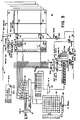
Referring now to Figure 3, there is illustrated a detailed block diagram of a frame
buffer 50 designed in accordance with the present invention while Figure 5
illustrates a method in accordance with the invention. Figure 3 illustrates a circuit
board upon which reside the various components of a frame buffer 50. The frame
buffer 50 includes a plurality of memory cells 53 such as field effect transistor
devices arranged to provide a dynamic random access memory array 52. The
arrangement of the cells 53 constituting the array 52 is developed in accordance
with principals well known to those skilled in the art. It is adapted to provide a
sufficient number of addressable memory cells 53 in the array 52 to describe the
number of pixels to be presented on an output display device in a particular mode of
operation. For example, the array 52 may include a total of thirty-two planes (only
the first is illustrated in detail in Figure 3), each plane including 256 rows, each
row including 1024 memory devices; such an arrangement allows the storage of
color data sufficient to display thirty-two bit color in a 512 X 512 pixel display on a
color output display terminal. Although the frame buffer 50 may display both
thirty-two bit and sixteen bit color modes as well as other modes well known to
those skilled in the art, the frame buffer 50 is particularly adapted for use with
pixels displaying color in eight bit color modes.
In addition to the array 52, the frame buffer 50 includes row and column decode
circuitry for decoding the addresses furnished by a controller such as a central
processor and selecting individual memory cells in each plane of the array 52 to
define the various pixels which may be represented on an output display device.
The address decoding circuitry includes row decoding circuitry 54 and column
decoding circuitry 56 by which individual memory cells 53 representing bits of
individual pixels may be selected for reading and writing. Also included as a part
of the frame buffer 50 are data conductors 58 which may be connected to a data bus
to provide data to be utilized in the array 52. Typically, thirty-two data conductors
58 are provided although this number will vary with the particular computer
system. The number thirty-two matches the number of bits which are transferred to
indicate the color of a single pixel of the largest number of bits expected to be used
by the display system in the most accurate color mode of operation.
When data is written to the frame buffer 50 on the conductors 58 of the data bus in
the normal mode of operation, each group of thirty-two bits defines one or more
color values to be displayed at one or more pixel positions on the output display.
Thus, when an output display is displaying data in an eight bit color mode, the
thirty-two bits carried by the data conductors 58 in normal write mode may define
four pixel positions on the display. On the other hand, when a display is
displaying data in a thirty-two bit color mode, the thirty-two bits of the data
conductors 58 carry information defining a single pixel position on the display. As
may be seen, one of the data conductors 58 of the bus is connected through an
input data buffer to all of eight multiplexors 62 in each plane of the array. The
embodiment illustrated in Figure 3 is particularly adapted to be used in a system
utilizing eight bit color modes; and, to this end, the system utilizes eight individual
multiplexors 62 in each plane of the frame buffer 50 for selecting particular write
input data. Each of these multiplexors 62 has its output connected to one of eight
tri-state write drivers 73 which furnishes an output signal via a write enable switch
such as a transmission gate 71 on a conductor 66 connected to every eighth column
of the particular plane of the array. Each of the multiplexors 62 selects the source
of the data to be transferred to the array 52 in each plane depending on the mode of
operation selected. Thus, in normal mode, the data bit is selected directly from the
data conductor 58 for that plane of the array. The bit is transferred from one of the
multiplexors 62 by one of the eight write drivers 73 to a particular selected column
and written to the memory cell 53 at that column and the selected row. Since a bit
may be written in each of thirty-two planes of the array, thirty-two bits may be
written from the bus conductors 58 (one to each plane) as one thirty-two bit pixel,
two sixteen bit pixels, or four eight bit pixels, depending on the color mode in
which the system is operating.
As is shown in Figure 3, a mode control circuit 68 is provided to designate the
particular mode of operation in which the frame buffer is to operate. To accomplish
mode selection, four control signals DSF0-DSF3 are furnished along with write
enable and output enable signals. The combination of these signals produces the
particular output mode control signals in a manner well known to those skilled in
the prior art.
In a normal mode write operation as practiced in the prior art, a particular address is
transferred on the address bus to select a particular row and column. The row
address is furnished to the row decode circuitry 54 by a row address latch 51 on the
falling edge of a row address strobe signal. The row address causes power to be
furnished to all of the memory cells 53 joined to the particular row of the array in
each of the selected planes. Once power has been furnished to the appropriate row
of the array, the value of each memory cell in the row is sensed by a sense amplifier
63 for each column of the array. The sense amplifiers 63 are turned on, and each
sense amplifier 63 drives the value sensed back to refresh the memory cell 53 in the
selected row.
At the falling edge of the CAS signal, the column address is transferred from a latch
57 and applied to the appropriate switches 67 of the column decode circuitry 56 to
select the appropriate columns in each plane to be written. In embodiment of the
frame buffer 50 illustrated, the column address is ten bits. Of these ten bits, the
higher valued seven bits CA3-9 of the column address are used to select a group of
eight adjacent columns. The normal mode write control signal at each of the
multiplexors 62 causes the data signal furnished on the single conductor 58
associated with that plane to be transferred from the data input buffer by each of the
eight multiplexors 62. One of the signals produced by the multiplexors 62 is
amplified by a single one of the write drive amplifiers 73 and transferred to the
addressed memory cell 53 in that plane of the array. The lower three bits CA0-2 of
the column address from the latch 57 select the particular one of the eight write
drive amplifiers 73 which transfers the data bit to a single one of the columns.
Since each of the conductors 58 associated with each plane of the array 52 carries
an individual bit for the memory cell at the selected row and column, the pixel value
(or values) will be transferred to the appropriate column and row position in each
plane of the array.
In a similar manner, when a particular pixel value is to be read from the array 52 in
the normal mode of operation, the row and column addresses are transferred to the
decode circuitry 54 and 56. A row address is selected on the falling edge of the
RAS signal; and the entire row of memory cells in each selected plane of the array
52 is refreshed. At the falling edge of the CAS signal, the higher valued seven bits
CA3-9 of the column address are applied to the appropriate switches 67 of the
column decode circuitry 56 to select the eight adjacent columns in each plane which
have been addressed and are to be read. The condition of the memory cells 53 in
each of these eight columns of each selected plane are sensed by a second set of
output sense amplifiers 75. The output of a particular one of the columns is
selected by a multiplexor 79 in each plane which is controlled by the normal mode
read signal and the value of the lower three bits CA0-2 of the column address. This
causes the condition of a particular memory cell 53 to be transferred to a particular
one of the conductors 58 of the data bus associated with that plane of the array 52.
Thus, as has been illustrated, the frame buffer 50 carries out the typical normal read
and write modes of operation.
The frame buffer 50 also includes at least a pair of color value registers C0 and C1
which are utilized to store color values which may be used in color block modes of
operation described hereinafter in which a plurality of storage positions may be
written simultaneously. Each plane of the array includes a one bit register C0 and a
one bit register C1 for storing one bit of a color value. Since each plane includes
one bit for each register, each register C0 and C1 includes a total of thirty-two bits
in the preferred embodiment. Thus an entire eight bit color value may be stored in
the registers C0 and C1 residing on eight planes, an entire sixteen bit color value
may be stored in the registers C0 and C1 residing on sixteen planes, and an entire
thirty-two bit color value may be stored in the registers C0 and C1 of thirty-two
planes of the frame buffer 50. With a thirty-two bit color register such as is
shown, the color pattern for a particular eight bit color value may be repeated four
times in each color register (similarly a sixteen bit color may be repeated twice).
The color registers C0 and C1 may be selectively addressed so that they may be
loaded by data furnished on the conductors 58 of the data bus; as may be seen,
switches are provided in each cell plane to allow loading of the registers C0 and C1
with color value data from the data conductors 58. The details of the color block
registers and their use are described in the U.S. patent 5,504,855.
entitled Apparatus For Providing Fast Multi-Color Storage In A Frame Buffer.
Priem et al.
The color registers C0 and C1 provide color values which the multiplexors 62 may
select for writing to the cells of the memory array instead of the data furnished on
the conductors 58. The selection by the multiplexors 62 of color values from the
registers C0, C1 or of pixel data from the conductors 58 depends on the particular
color mode of operation, a value indicated by control signals furnished by the
central processor or by an associated graphical accelerating device.
When a color block mode of operation is indicated by the control signals, the data
conductors 58, rather than carrying pixel data, carry enabling signals to indicate
pixel positions in the array 52 to which the color values held in the registers C0 and
C1 are to be written. These color values are initially loaded from the data
conductors 58 of each array plane of the frame buffer 50 in response to a load color
register control signal. Since two color registers C0 and C1 are provided in the
preferred embodiment, a total of four color block modes of operation are possible.
These modes are referred to as color 0 mode, color 1 mode, color 0&1 mode, and
color 1&0 mode. As will be seen, substantial time is saved with any of these
modes of operation simply through the lack of a requirement to load the color value
registers for writing to each row of the display.
In the color 0 mode of operation, if a control signal value of one is transferred on a
particular data conductor 58, then the value in the color register C0 is written to the
storage positions controlled by that conductor 58. The value in the color register
C0 is also transferred to all other storage positions by data conductors 58 which
transfer a control signal with a one value. On the other hand, no color value is
written to the pixel positions controlled by a data conductor 58 on which a zero
control value is transferred. Thus, thirty-two different pixel positions may be
affected in a single simultaneous transfer; those positions which receive a one value
are enabled to receive the value in the color register C0 while those which receive a
zero value remain unchanged.
The manner in which this is accomplished will be illustrated in a case of eight bit
color. Presuming that the color value register C0 has been loaded with a color
value pattern of eight bits which is repeated four times in the thirty-two bits
provided in that register and that the color value register C1 has been loaded with
another color value pattern of eight bits which is repeated four times in the thirty-two
bits provided in that register, then a row and eight columns are selected by the
address on the address bus through the row and column address decode circuitry
54 and 56 in the manner described above. Assuming that color block mode 0 is
selected, all eight of the multiplexors 62 of each plane select the register C0 as the
source of color data for the array. Then the particular write drivers 73 are enabled
in accordance with the enabling signals appearing on the conductors 58 of the data
bus.
The control data appearing on the conductors 58 is sent to a pixel mask register 55.
The bits of the pixel mask register 55 are used in the manner illustrated in Figure 4
in each of the array planes to control all of the drivers 73 controlling transfer of data
to a particular pixeL Since the example considered involves eight bit color and
assuming that the first eight columns have been selected by the column address, the
bits defining the first pixel lie in the first column in the selected row and the first
eight planes of that column. The first pixel P1 in the pixel mask register 55
controls the appropriate drivers 73 controlling the first column and the first eight
planes to transfer the color to these bit positions in the array from the color value
register C0. Consequently, with one row and eight columns selected, a total of
thirty-two eight bit color pixels may be written simultaneously with the value stored
in the color value register C0.
This is a fast mode of operation similar to the four bit block mode used in prior art
frame buffers and may be used to clear the screen very rapidly or to otherwise
provide a single color to the window area. For example, a frame buffer 30 for a
display which is 1024 X 780 pixels and eight bits deep, may be cleared
approximately thirty-two times faster than individual pixels may be written one by
one to the frame buffer 50. This mode is also useful for clipping since a color
value may be written to pixel positions inside a window area while the pixel
positions outside that window area are not enabled.
Color 1 mode is similar to color 0 mode except that if a one value is transferred on a
particular data conductor 58, then the value in the color register C1 is written to the
storage positions which define the pixel addressed for that conductor 58. The value
in the color register C1 is also transferred to all other storage positions at addresses
enabled by one values transferred on the data conductors 58. On the other hand, no
color value is written to the pixel positions to which a zero is transferred on the data
conductors.
As may be seen, since the two color registers C0 and C1 may be loaded prior to
manipulating any portion of a window and are always available, a series of pixels
(e.g., thirty-two) may be written and clipped in two accesses without any need to
reload color registers. Background color may be written in a first access and
foreground color written in a second access without any need to reload a color
register between accesses.
However, even faster writing is possible using the color modes 0&1 and 1&0 in
those portions of the display in which clipping is unnecessary. As is pointed out in
the co-pending patent application referred to above, most operations involved in
writing to the display utilize two colors. Typically, a rendering chip (graphics
accelerator) or the central processing unit provides a control signal indicating where
clipping is necessary. In the absence of this signal, use of the modes 0&1 and 1&0
allow two colors to be written simultaneously to the frame buffer. In these modes a
zero value on a data conductor 58 indicates that a color value is to be written to the
controlled pixels from one color value register while a one value on a data
conductor 58 indicates that a color value is to be written to the controlled pixels
from the other color value register.
This is accomplished by combining the control value transferred on the data
conductor 58 for each plane and stored in the pixel mask register 55 with the color
mode control signal to select the particular color register from which the color value
is transferred by each of the multiplexors 62. For example, when in color mode
0&1 or 1&0, a zero in a bit position in the pixel mask register 55 causes a
multiplexor 62 to select the color value stored in one color value register while a
one in a bit position in the pixel mask register 55 causes a multiplexor 62 to select
the color value stored in the other color value register. Then, the color mode
control signals indicating mode 0&1 or 1&0 control all of the pixels selected to be
written by the drivers 73 to the array. This allows two separate colors representing
both foreground and background to be written simultaneously to those portions of a
window area which do not require clipping.
The provision of the two color value registers allows a number of new methods of
writing data to the frame buffer to be practiced in addition the color modes
described. For example, in addition to writing in groups of thirty-two pixels at
once using the color registers C0 and C1, block modes are provided by which an
entire row of pixels may be written from the color registers in one color with
clipping or in two colors undipped. These modes are referred to as block 256,
block 512 and block 1024 modes and are described in detail in the U.S. patent
5,533,187 entitled Multiple Block Mode Operations In A Frame
Buffer System Designed For Windowing Operations, Priem et al.
In block 256 mode, the value on each data conductor determines the color value
which is written to thirty-two adjacent eight bit pixel positions. This is
accomplished by the column address selecting one quarter of the total of columns
(256) in each plane of the array simultaneously. Then each of the pixels connected
to each of these columns receives the single color value in a color value register
designated by the value carried on the data conductor in the particular color mode.
It will be seen that in block 256 mode a total of thirty-two times thirty-two eight bit
pixels (1024 pixels) are affected at once by each write access. This is a typical
number of pixels in a row of a modern computer color monitor. Thus, each access
of eight bit pixels in block 256 mode may write all of the pixels in a 1024 pixel
row. It will be appreciated that this mode may be used to very rapidly clear an
entire screen or to write a pattern which varies in thirty-two bit blocks on the
screen.
However, in any case in which two colors are written to the frame buffer in the
same access using the block 256 mode, the data conductors are not available to
provide clipping signals. For this reason, it is necessary to utilize the color 0 and
color 1 modes at the boundaries of a window in order to accomplish clipping of the
window. These single color modes may be used at the window crossings at each
side of each row containing a window to write a background color to the window
edge on a first access and then to write a foreground color to the window edge on a
second access. In a similar manner, because the granularity of the access is so
large with the block 256 mode, it often must be used with the other modes to clip to
a window edge. That is, since each control bit affects thirty-two pixels, block 256
mode can only select pixels to write and not write in adjacent groups of thirty-two
pixels. Consequently, the block 256 mode must be used with block 8 mode to clip
to an exact window edge.
A second additional mode is referred to as block 512 mode. In block 512 mode
each data conductor affects the value of data written to thirty-two adjacent sixteen
bit pixel positions. In this mode, the column address selects a total of half the
columns in each plane simultaneously. This mode requites the increase in number
of selection conductors, multiplexors 62, and other components discussed above to
sixteen. This mode is used with the block 16 mode in the same manner that block
256 mode is used with block 8 mode to rapidly write to an entire row within a
clipped window area of the display. A third additional mode is referred to as block
1024 mode. In block 1024 mode, all of the columns in each plane are selected
simultaneously by the column address. This mode requires the increase in number
of selection conductors, multiplexors 62, and other components discussed above to
thirty-two. In block 1024 mode, each data conductor affects the value of data
written to thirty-two adjacent thirty-two bit pixel positions. This mode is used with
the block 32 mode in the same manner that block 256 mode is used with block 8
mode to rapidly write to an entire row within a clipped window area of the display.
Each of these modes provides useful functions in the same manner as does block
256 mode but for configurations of frame buffers storing data describing sixteen bit
and thirty-two bit pixels.
In addition to the color values registers C0 and C1 which provide fast operation,
the frame buffer 50 of Figure 3 includes output circuitry by which pixel data is
shifted to an output display device (not shown in the figure). This includes a an
array of transmission gates 77 which is utilized to shift data eight bits at a time from
each plane of the array to an output shift register 80. The shift register 80 in each
plane includes a total of sixty-four bit positions. Thus, the register totals 256 bytes
in the thirty-two planes of the preferred embodiment, a value equivalent to one-fourth
of a row on a display having 1024 pixel positions in a row. The data in the
register 80 is then shifted a bit at a time from each plane by another multiplexor 82
to a circuitry controlling the display of the pixel data on an output display device. It
will be recognized that this shift register is substantially smaller than that typically
used at the output of a frame buffer and consequently uses much less circuit board
area.
The frame buffer 50 also includes circuitry designed to provide an extremely rapid
scrolling operation. The scrolling operation is described in detail in U.S. patent
5,805,133 entitled METHOD AND APPARATUS FOR
INCREASING THE RATE OF SCROLLING IN A FRAME BUFFER SYSTEM
DESIGNED FOR WINDOWING OPERATIONS, Priem et al -
That scrolling operation is described, in general, at this point in order to
explain the use of the various circuitry of the frame buffer.
In the scrolling operation, the data is first read from the array and then written back
to the array to a new row without being removed from the frame buffer 50. In
order to accomplish this, a scroll mode signal is initiated by the controlling circuitry
(central processor or graphics accelerator); and an address is furnished to the row
and column decode circuitry to designate the particular data to be scrolled. The
scroll mode may cause a particular row to be selected at the falling edge of a RAS
signal as in normal mode of operation and the memory cells of that row to be
refreshed. The higher order bits of the column address are used to select eight
adjacent columns of the address. The mode signal at the array of transmission
gates 77 of each plane causes the data in the memory cells of each of the eight
columns selected to be transferred to a first eight bit latch shown as latch 0 in the
figure. A next sequential address causes the data in the memory cells of each of the
next eight columns to be selected and to be transferred to a second eight bit latch
shown as latch 1 in the figure. This continues for two more read operations which
select two more sets of eight memory cells in each plane and place the results read
in third and fourth eight bit latches latch 2 and latch 3.
Thus, in a set of four read operations taking only 180 ns (one RAS/CAS of 120 ns.
followed by three CAS cycles of 20 ns. each), a total of thirty-two bits in each of
thirty-two planes is read and stored in the Latches 0-3. This means that in four
individual accesses requiring in total a single RAS signal and a four CAS signals
taking 180 ns., a total of 128 eight bit pixels, may be stored in the latches 0-3.
Thus, an entire row of pixels on a display 1024 pixels wide may be accessed and
stored in a total period of eight times 180 ns. or 1440 ns.
As is shown in Figure 3, each latch 0-3 is connected so that its individual bits may
be selected by a multiplexor 81 to be furnished to the multiplexors 62. In the
figure, one of the latches 0-3 is illustrated with each of its bit positions furnishing
input to each of the eight individual multiplexors 62 of that memory plane. This
allows four sequential write operations to four consecutive addresses, taking
approximately 180 ns., to write the data being scrolled back to the new row
positions in the array 52 to which the row is addressed. As with the scroll read
operation, the scroll mode control signal causes the higher bits of the column
address to select the appropriate eight adjacent columns in each write operation.
The scroll mode control signal then selects all of the columns using the drivers 73
and the write enable switches 71. In each write back operation used in scrolling,
the values in each of the individual bit latches 0-3 are then driven onto the array by
overdriving the sense amplifiers 63 to establish the new values at the selected
memory positions in the appropriate cells of the array. Thus, the total time required
to read and write back the data to scroll 128 pixels is only 180 ns. while a row
requires 1440 ns., approximately one-85th of the time required to scroll in prior art
arrangements.
An additional facility of the invention allows it to clip pixel data to fit windows in
which that data is stored at the same time that scrolling is taking place. It will have
been noted that during any period in which scrolling is occurring, the conductors
58 on the data bus are not being used for the scrolling. By sending enabling
signals on the data conductors 58 to the write enable gates 71 of each array,
clipping may be accomplished. For example, if a first data conductor 58 carries a
zero indicating that a write is not to occur and that signal is applied to disable the
transmission gates 71 connected to all of the conductors 66 (one in each plane of
the array 52) affecting the bits of a particular pixel, then the bits in the particular
latch bit position will not be written. Thus an entire pixel may be clipped. If all of
the data conductors controlling pixel positions outside a window carry zero values,
then the entire area outside a window may be clipped while the scrolling is
occurring.