EP0678907B1 - Method for fabricating reverse-staggered thin-film transistor - Google Patents
Method for fabricating reverse-staggered thin-film transistor Download PDFInfo
- Publication number
- EP0678907B1 EP0678907B1 EP95105936A EP95105936A EP0678907B1 EP 0678907 B1 EP0678907 B1 EP 0678907B1 EP 95105936 A EP95105936 A EP 95105936A EP 95105936 A EP95105936 A EP 95105936A EP 0678907 B1 EP0678907 B1 EP 0678907B1
- Authority
- EP
- European Patent Office
- Prior art keywords
- layer
- type
- amorphous silicon
- film transistor
- thin
- Prior art date
- Legal status (The legal status is an assumption and is not a legal conclusion. Google has not performed a legal analysis and makes no representation as to the accuracy of the status listed.)
- Expired - Lifetime
Links
- 238000000034 method Methods 0.000 title claims description 34
- 239000010409 thin film Substances 0.000 title claims description 24
- 229910021417 amorphous silicon Inorganic materials 0.000 claims description 41
- 239000010408 film Substances 0.000 claims description 20
- PZPGRFITIJYNEJ-UHFFFAOYSA-N disilane Chemical compound [SiH3][SiH3] PZPGRFITIJYNEJ-UHFFFAOYSA-N 0.000 claims description 16
- BLRPTPMANUNPDV-UHFFFAOYSA-N Silane Chemical compound [SiH4] BLRPTPMANUNPDV-UHFFFAOYSA-N 0.000 claims description 14
- 239000007789 gas Substances 0.000 claims description 13
- 238000005268 plasma chemical vapour deposition Methods 0.000 claims description 12
- 239000012535 impurity Substances 0.000 claims description 7
- 229910021420 polycrystalline silicon Inorganic materials 0.000 claims description 7
- 238000000927 vapour-phase epitaxy Methods 0.000 claims description 6
- 238000000151 deposition Methods 0.000 claims description 5
- 229910007264 Si2H6 Inorganic materials 0.000 claims description 3
- 238000004519 manufacturing process Methods 0.000 claims description 2
- 239000000463 material Substances 0.000 claims 3
- 239000004065 semiconductor Substances 0.000 claims 3
- 239000010410 layer Substances 0.000 description 52
- 229910000077 silane Inorganic materials 0.000 description 11
- 230000001681 protective effect Effects 0.000 description 8
- 239000000758 substrate Substances 0.000 description 8
- 229910052581 Si3N4 Inorganic materials 0.000 description 7
- HQVNEWCFYHHQES-UHFFFAOYSA-N silicon nitride Chemical compound N12[Si]34N5[Si]62N3[Si]51N64 HQVNEWCFYHHQES-UHFFFAOYSA-N 0.000 description 7
- MHAJPDPJQMAIIY-UHFFFAOYSA-N Hydrogen peroxide Chemical compound OO MHAJPDPJQMAIIY-UHFFFAOYSA-N 0.000 description 6
- 229920005591 polysilicon Polymers 0.000 description 6
- PNEYBMLMFCGWSK-UHFFFAOYSA-N aluminium oxide Inorganic materials [O-2].[O-2].[O-2].[Al+3].[Al+3] PNEYBMLMFCGWSK-UHFFFAOYSA-N 0.000 description 5
- 230000003247 decreasing effect Effects 0.000 description 3
- 230000008021 deposition Effects 0.000 description 3
- 239000007792 gaseous phase Substances 0.000 description 3
- 239000001257 hydrogen Substances 0.000 description 3
- 229910052739 hydrogen Inorganic materials 0.000 description 3
- 125000004435 hydrogen atom Chemical class [H]* 0.000 description 3
- XKRFYHLGVUSROY-UHFFFAOYSA-N Argon Chemical compound [Ar] XKRFYHLGVUSROY-UHFFFAOYSA-N 0.000 description 2
- VYZAMTAEIAYCRO-UHFFFAOYSA-N Chromium Chemical compound [Cr] VYZAMTAEIAYCRO-UHFFFAOYSA-N 0.000 description 2
- XUIMIQQOPSSXEZ-UHFFFAOYSA-N Silicon Chemical compound [Si] XUIMIQQOPSSXEZ-UHFFFAOYSA-N 0.000 description 2
- 125000004429 atom Chemical group 0.000 description 2
- 229910052804 chromium Inorganic materials 0.000 description 2
- 239000011651 chromium Substances 0.000 description 2
- 238000011109 contamination Methods 0.000 description 2
- 238000009826 distribution Methods 0.000 description 2
- 150000002500 ions Chemical class 0.000 description 2
- 229910052751 metal Inorganic materials 0.000 description 2
- 239000002184 metal Substances 0.000 description 2
- 229910052710 silicon Inorganic materials 0.000 description 2
- 239000010703 silicon Substances 0.000 description 2
- ZOXJGFHDIHLPTG-UHFFFAOYSA-N Boron Chemical compound [B] ZOXJGFHDIHLPTG-UHFFFAOYSA-N 0.000 description 1
- UFHFLCQGNIYNRP-UHFFFAOYSA-N Hydrogen Chemical compound [H][H] UFHFLCQGNIYNRP-UHFFFAOYSA-N 0.000 description 1
- 229910052782 aluminium Inorganic materials 0.000 description 1
- XAGFODPZIPBFFR-UHFFFAOYSA-N aluminium Chemical compound [Al] XAGFODPZIPBFFR-UHFFFAOYSA-N 0.000 description 1
- 238000000137 annealing Methods 0.000 description 1
- 229910052786 argon Inorganic materials 0.000 description 1
- 239000012298 atmosphere Substances 0.000 description 1
- 230000015572 biosynthetic process Effects 0.000 description 1
- 229910052796 boron Inorganic materials 0.000 description 1
- 150000001768 cations Chemical class 0.000 description 1
- 239000000470 constituent Substances 0.000 description 1
- 230000002542 deteriorative effect Effects 0.000 description 1
- 238000007599 discharging Methods 0.000 description 1
- 238000001312 dry etching Methods 0.000 description 1
- 230000000694 effects Effects 0.000 description 1
- 230000005684 electric field Effects 0.000 description 1
- 230000005611 electricity Effects 0.000 description 1
- 238000005530 etching Methods 0.000 description 1
- 239000011521 glass Substances 0.000 description 1
- 239000011261 inert gas Substances 0.000 description 1
- 239000004973 liquid crystal related substance Substances 0.000 description 1
- 238000001459 lithography Methods 0.000 description 1
- 239000000203 mixture Substances 0.000 description 1
- 229910021421 monocrystalline silicon Inorganic materials 0.000 description 1
- 239000012299 nitrogen atmosphere Substances 0.000 description 1
- TWNQGVIAIRXVLR-UHFFFAOYSA-N oxo(oxoalumanyloxy)alumane Chemical compound O=[Al]O[Al]=O TWNQGVIAIRXVLR-UHFFFAOYSA-N 0.000 description 1
- 238000004886 process control Methods 0.000 description 1
- 239000011241 protective layer Substances 0.000 description 1
- 238000007086 side reaction Methods 0.000 description 1
- 238000004544 sputter deposition Methods 0.000 description 1
- 239000012808 vapor phase Substances 0.000 description 1
- 238000001039 wet etching Methods 0.000 description 1
Images

Classifications
-
- H—ELECTRICITY
- H01—ELECTRIC ELEMENTS
- H01L—SEMICONDUCTOR DEVICES NOT COVERED BY CLASS H10
- H01L21/00—Processes or apparatus adapted for the manufacture or treatment of semiconductor or solid state devices or of parts thereof
- H01L21/02—Manufacture or treatment of semiconductor devices or of parts thereof
- H01L21/04—Manufacture or treatment of semiconductor devices or of parts thereof the devices having at least one potential-jump barrier or surface barrier, e.g. PN junction, depletion layer or carrier concentration layer
- H01L21/18—Manufacture or treatment of semiconductor devices or of parts thereof the devices having at least one potential-jump barrier or surface barrier, e.g. PN junction, depletion layer or carrier concentration layer the devices having semiconductor bodies comprising elements of Group IV of the Periodic System or AIIIBV compounds with or without impurities, e.g. doping materials
-
- H—ELECTRICITY
- H01—ELECTRIC ELEMENTS
- H01L—SEMICONDUCTOR DEVICES NOT COVERED BY CLASS H10
- H01L29/00—Semiconductor devices adapted for rectifying, amplifying, oscillating or switching, or capacitors or resistors with at least one potential-jump barrier or surface barrier, e.g. PN junction depletion layer or carrier concentration layer; Details of semiconductor bodies or of electrodes thereof ; Multistep manufacturing processes therefor
- H01L29/66—Types of semiconductor device ; Multistep manufacturing processes therefor
- H01L29/66007—Multistep manufacturing processes
- H01L29/66075—Multistep manufacturing processes of devices having semiconductor bodies comprising group 14 or group 13/15 materials
- H01L29/66227—Multistep manufacturing processes of devices having semiconductor bodies comprising group 14 or group 13/15 materials the devices being controllable only by the electric current supplied or the electric potential applied, to an electrode which does not carry the current to be rectified, amplified or switched, e.g. three-terminal devices
- H01L29/66409—Unipolar field-effect transistors
- H01L29/66477—Unipolar field-effect transistors with an insulated gate, i.e. MISFET
- H01L29/66742—Thin film unipolar transistors
- H01L29/6675—Amorphous silicon or polysilicon transistors
- H01L29/66765—Lateral single gate single channel transistors with inverted structure, i.e. the channel layer is formed after the gate
-
- H—ELECTRICITY
- H01—ELECTRIC ELEMENTS
- H01L—SEMICONDUCTOR DEVICES NOT COVERED BY CLASS H10
- H01L29/00—Semiconductor devices adapted for rectifying, amplifying, oscillating or switching, or capacitors or resistors with at least one potential-jump barrier or surface barrier, e.g. PN junction depletion layer or carrier concentration layer; Details of semiconductor bodies or of electrodes thereof ; Multistep manufacturing processes therefor
- H01L29/66—Types of semiconductor device ; Multistep manufacturing processes therefor
- H01L29/68—Types of semiconductor device ; Multistep manufacturing processes therefor controllable by only the electric current supplied, or only the electric potential applied, to an electrode which does not carry the current to be rectified, amplified or switched
- H01L29/76—Unipolar devices, e.g. field effect transistors
- H01L29/772—Field effect transistors
- H01L29/78—Field effect transistors with field effect produced by an insulated gate
- H01L29/786—Thin film transistors, i.e. transistors with a channel being at least partly a thin film
Definitions
- the present invention relates to a method for fabricating a thin-film transistor and, more particularly, to a method for fabricating a reverse-staggered thin-film transistor employed in a liquid crystal display device.
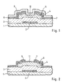
- Fig. 1 shows a conventional thin-film transistor of an amorphous silicon.
- This thin-film transistor is constituted by a gate electrode 2, a gate insulating film 3 made of a silicon nitride film, an intrinsic amorphous silicon layer 4 and an n-type amorphous silicon contact layer 5, a drain electrode 6 and a source electrode 7.
- a protective layer 9 made of silicon nitride is further formed to cover the transistor.
- the surface portion 10 of the amorphous silicon layer 4 between the drain electrode 6 and the source electrode 7 is sometimes called a "back channel" and has one of key factors determining the characteristics of the transistor.
- a leak current is caused to increase and thus flows between the source and drain. Even if the back channel 10 is not contaminated, the positive electric charges due to the contamination on the protective film 9 increase an electric field applied the back channel 10 up to or more than the threshold of the back channel. A leakage current thereby flows. Besides, the protective film 9 itself may be charged positively, so that the leak current also flows.
- such a thin-film transistor is disclosed in Japanese Patent Laid-Open No. Hei 2-163972 that a back channel covered with an oxide film obtained from hydrogen peroxide or with an alumina film formed by the CVD process. Such a film can convert the back channel into a p-type one. The leakage current is thereby decreased.
- the p-type back channel thus converted depends on the quality of the oxide or the alumina film and is thus inferior in controllability.
- the drain and source electrodes are damaged by the hydrogen peroxide.
- alumina in the alumina film may be diffused into the amorphous silicon layer to change the property of a thin-film transistor.
- FIG. 2 there are shown another thin-film transistor which is disclosed in Japanese Patent Publication No. Hei 5- 083197, in which the same constituents as those shown in Fig. 4 are denoted by the same reference numerals.
- a similar method for fabricating a thin-film transistor is known from US-A-5 114 896.
- a portion of the n-type contact layer 5 which is not covered with the drain and source electrodes 6 and 7 is converted into a p-type region 11 by adding p-type impurities therein.
- the back channel is thereby covered with the p-type region 11.
- the contact layer 5 has a considerably high impurity concentration of 10 20 atoms/cm 3 or more. For this reason, it is necessary to dope the p-type impurities at a very high concentration. Such very highly doping lacks in controllability, however. Moreover, the very highly doped region 11 results in increase of the leakage current.
- the thin-film transistor fabrication method of the present invention it is possible to provide a structure in which a p-type amorphous silicon layer or a p-type polysilicon layer is formed uniformly on an intrinsic amorphous silicon layer directly.
- the method has an advantage of preventing the leak current of a transistor which is increased due to contamination by cations coming from the outside and electron generation in a back channel by electrification of the protective film.
- p-type amorphous or p-type polysilicon can selectively be deposited on amorphous or polysilicon by exposing it to the gaseous phase of disilane containing diborane or silane, and there is no such side reaction as wiring is affected, aluminum diffuse in an amorphous or polysilicon layer, or process control is difficulty, a large advantage can be obtained.
- the plasma CVD process there is an advantage that the film forming rate is high though the selectivity is low.
- the method of the present invention for fabricating a thin-film transistor is characterized in that p-type amorphous silicon layer with a thickness of 100 ⁇ or less containing no n-type doped impurities is formed on a back channel of the intrinsic amorphous silicon directly. Because of containing no n-type doped impurities, impurity density of the p-type amorphous silicon layer is not so high that prevents current leakage according to uniformless ion distribution of the layer. Furthermore, it gets more uniformal ion distribution according to obtaining by gaseous phase of disilane or silane gas containing diborane.
- the method of the present invention is characterized in that the p-type amorphous silicon layer can be obtained by exposing the intrinsic amorphous silicon layer to the gaseous phase of disilane or silane gas containing diborane. Furthermore, it is possible to use polysilicon instead of amorphous silicon.
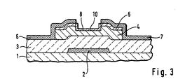
- a thin-film transistor fabricated by a method according an embodiment of the present invention has a gate electrode 2 selectively formed on an insulating substrate 1, a gate insulating film 3 an intrinsic or non-doped amorphous silicon layer 4, an n-type amorphous silicon contact layer 5, a drain electrode 6, and a source electrode 7.
- This transistor further has a p-type amorphous silicon layer 8 on the back channel portion of the amorphous silicon layer 4 between the drain electrode 6 and the source electrode 7 in accordance with the present invention.
- the thickness of p-type amorphous silicon layer 8 is 100 ⁇ or less.
- a protective such as silicon-nitride covers the p-type amorphous silicon layer 8 and a the source and drain electrodes 6 and 7.
- the above thin-film transistor is fabricated as follows:
- the gate electrode 2 made of a metal such as chromium is selectively formed on the insulating substrate 1 made of a glass or the like, followed by forming the gate insulating film 3 made of silicon nitride over the entire surface.
- the intrinsic or non-doped amorphous silicon layer 4 and the n-type amorphous silicon contact layer 5 are thereafter deposited in that order by the plasma CVD method.
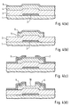
- the amorphous silicon layer 4 and the n-type amorphous silicon contact layer 5 are selectively etched to form an island by the lithography art, as shown in Fig. 4(b).
- a metal film made of chromium or the like is deposited over the entire surface by the sputtering method and then patterned to form the drain electrode 6 and the source electrode 7 as shown in Fig. 4(c).
- the portion of the n-type amorphous silicon contact layer 5 between the drain electrode 6 and the source electrode 7 is removed by using the electrodes as a mask by the wet etching method or the dry etching method in accordance with the present invention. This etching process is carried out until the surface portion of the amorphous silicon layer 4 is removed. That portion of the contact layer 5 is thus completely removed, the surface of the amorphous silicon layer 4 thus exposed serves as a back channel 10, as shown in Fig. 4(d).
- the p-type amorphous silicon layer 8 is then selectively deposited between the drain electrode 6 and the source electrode 7 in accordance also with the present invention. Finally the silicon-nitride protective film 9 is formed.
- the selective deposition of the p-type amorphous silicon layer 8 only on the exposed amorphous silicon layer is performed by mixing disilane Si 2 H 6 , hydrogen H 2 and diborane B 2 H 6 at the ratio of 3:2:6, setting the pressure of the mixed gas to 200 Pa and the substrate temperature to 350°C, and exposing the thin-film transistor shown in Fig. 4(d) to the mixed-gas atmosphere.
- the thickness of the layer 8 is several tens of angstroms though it cannot accurately be measured because the deposition rate is very low. Under the above conditions, the depositing time for the layer 8 can be approx. 15 min. Thereafter, the layer 8 is annealed in the nitrogen atmosphere at 250°C for 30 min.
- silane instead of disilane in the mixed gas.
- silane is not easily decomposed only by raising temperature. Therefore, it is better to use disilane.
- the ratio of disilane Si 2 H 6 to diborane B 2 H 6 of the mixed gas is set to 1:2.
- the ratio of hydrogen gas can be changed within the range of 0 to 10 when assuming the ratio of disilane as 1.
- an inert gas such as argon
- the temperature of the substrate in the range of 300 to 400°C.
- the temperature goes out of the range, it is difficult to perform the vapor-phase epitaxy. Because it is enough to deposit a p-type amorphous silicon layer up to the thickness of 10 to 100 ⁇ in a vapor phase, the layer can be deposited for 10 to 30 min. If the layer is too thick, there is a problem that leak current may flow. If the layer is too thin, it can not be formed uniformly. The annealing time is enough for 30 min to 2 hr.
- the p-type amorphous silicon layer 8 is obtained at a very low deposition rate, it is easily influenced by a substrate due to the same effect as the epitaxial art for single-crystal silicon and thus it is selectively deposited only on the intrinsic amorphous silicon layer 4. Therefore, the layer 8 is preferable because it is hardly deposited on areas of the substrate other than the intrinsic amorphous silicon layer 4. Presence of the p-type amorphous silicon layer 8 can be confirmed by measuring the depth profile through the SIMS element analysis and it is found that boron is present in layers with a thickness of 50 ⁇ or less at a concentration of 10 18 to 10 19 atoms/cm 3 .
- Fig. 5 shows the property of the thin-film transistor of this embodiment.
- the current between drain and source to the gate voltage when applying the voltage of 10 V between the drain and source. From Fig. 5, it is understood that the current between the drain and the source is decreased for the gate voltage of -10 v to 0 V compared to the case of the prior art. That is, the leak current is decreased when the thin-film transistor is off.
- increase of the off current is not recognized even by applying +30 V to the gate electrode and 0 V to the source electrode for 90 min in the air of 80°C. This is because the p-type silicon layer directly contacts the silicon-nitride protective film 9 and a stable interface is formed.
- the p-type amorphous silicon layer 8 with a thickness of several tens of angstroms is formed by mixing silane SiH 4 , hydrogen H 2 , and diborane B 2 H 6 at a mixing ratio of 1:1:2, setting the pressure of the mixed gas to 100 Pa (0.75 Torr), the substrate temperature to 300°C, and the electric power to 25 mW/cm 2 , and discharging electricity for 10 sec.
- the plasma CVD process an advantage is obtained that a p-type amorphous silicon layer can be formed for several tens of seconds though the selectivity is low.
- disilane and diborane for the vapor-phase epitaxy process.
- plasma CVD it is better to use silane and diborane.
- disilane for the plasma CVD.
- disilane is more easily decomposed than silane and therefore it is extremely decomposed due to plasma, disilane is not suitable for the plasma CVD.
- plasma CVD plasma serve as an assistant to decompose silane. Therefore, the combination of disilane and diborane in the vapor-phase epitaxy process corresponds to the combination of silane and diborane in the plasma CVD process.
- the mixing ratio of silane SiH 4 to diborane B 2 H 6 is set to 1:2 and hydrogen H 2 is mixed with the mixture of them in the range of 0 to 5.
- the pressure, substrate temperature, and electric power can be changed in the ranges of 80 to 120 Pa, 250 to 320°C, and 10 to 30 mW/cm 2 respectively. It is necessary to set the discharge time to several seconds to 1 min.
Description
- The present invention relates to a method for fabricating a thin-film transistor and, more particularly, to a method for fabricating a reverse-staggered thin-film transistor employed in a liquid crystal display device.
- Fig. 1 shows a conventional thin-film transistor of an amorphous silicon. This thin-film transistor is constituted by a
gate electrode 2, a gateinsulating film 3 made of a silicon nitride film, an intrinsic amorphous silicon layer 4 and an n-type amorphoussilicon contact layer 5, adrain electrode 6 and a source electrode 7. Aprotective layer 9 made of silicon nitride is further formed to cover the transistor. In this structure, thesurface portion 10 of the amorphous silicon layer 4 between thedrain electrode 6 and the source electrode 7 is sometimes called a "back channel" and has one of key factors determining the characteristics of the transistor. - Specifically, if
back channel 10 is contaminated and thus charged prior to the formation of theprotective film 9, a leak current is caused to increase and thus flows between the source and drain. Even if theback channel 10 is not contaminated, the positive electric charges due to the contamination on theprotective film 9 increase an electric field applied theback channel 10 up to or more than the threshold of the back channel. A leakage current thereby flows. Besides, theprotective film 9 itself may be charged positively, so that the leak current also flows. - In order to overcome such a problem, such a thin-film transistor is disclosed in Japanese Patent Laid-Open No. Hei 2-163972 that a back channel covered with an oxide film obtained from hydrogen peroxide or with an alumina film formed by the CVD process. Such a film can convert the back channel into a p-type one. The leakage current is thereby decreased.
- However, the p-type back channel thus converted depends on the quality of the oxide or the alumina film and is thus inferior in controllability. Moreover, when hydrogen peroxide is used, the drain and source electrodes are damaged by the hydrogen peroxide. In the case of the alumina film, on the other hand, alumina in the alumina film may be diffused into the amorphous silicon layer to change the property of a thin-film transistor.
- Another thin-film transistor is disclosed in Japanese Patent Laid-Open No. Hei 4-321275 to reduce the leakage current. In this transistor, an aluminum oxide layer is formed on a back channel. For this reason, this transistor also has the same problems as mentioned above.
- Turning to Fig. 2, there are shown another thin-film transistor which is disclosed in Japanese Patent Publication No. Hei 5- 083197, in which the same constituents as those shown in Fig. 4 are denoted by the same reference numerals. A similar method for fabricating a thin-film transistor is known from US-A-5 114 896.
In this device, a portion of the n-type contact layer 5 which is not covered with the drain andsource electrodes 6 and 7 is converted into a p-type region 11 by adding p-type impurities therein. The back channel is thereby covered with the p-type region 11. - However, the
contact layer 5 has a considerably high impurity concentration of 1020 atoms/cm3 or more. For this reason, it is necessary to dope the p-type impurities at a very high concentration. Such very highly doping lacks in controllability, however. Moreover, the very highlydoped region 11 results in increase of the leakage current. - It is therefore an object of the present invention to provide a method for fabricating a thin-film transistor of a low leakage current without deteriorating the characteristics thereof.
- It is another object of the present invention to provide a method for fabricating a thin-film transistor having a low leakage current by a simplified process.
- According to the thin-film transistor fabrication method of the present invention, it is possible to provide a structure in which a p-type amorphous silicon layer or a p-type polysilicon layer is formed uniformly on an intrinsic amorphous silicon layer directly.
- Therefore, the method has an advantage of preventing the leak current of a transistor which is increased due to contamination by cations coming from the outside and electron generation in a back channel by electrification of the protective film. Moreover, because p-type amorphous or p-type polysilicon can selectively be deposited on amorphous or polysilicon by exposing it to the gaseous phase of disilane containing diborane or silane, and there is no such side reaction as wiring is affected, aluminum diffuse in an amorphous or polysilicon layer, or process control is difficulty, a large advantage can be obtained. When using the plasma CVD process, there is an advantage that the film forming rate is high though the selectivity is low.
- Furthermore, there is an advantage that a high reliability is obtained because a p-type silicon layer directly contacts an amorphous or polysilicon layer and a silicon-nitride protective film and thereby a stable interface is obtained.
- The method of the present invention for fabricating a thin-film transistor is characterized in that p-type amorphous silicon layer with a thickness of 100 Å or less containing no n-type doped impurities is formed on a back channel of the intrinsic amorphous silicon directly. Because of containing no n-type doped impurities, impurity density of the p-type amorphous silicon layer is not so high that prevents current leakage according to uniformless ion distribution of the layer. Furthermore, it gets more uniformal ion distribution according to obtaining by gaseous phase of disilane or silane gas containing diborane. Moreover, the method of the present invention is characterized in that the p-type amorphous silicon layer can be obtained by exposing the intrinsic amorphous silicon layer to the gaseous phase of disilane or silane gas containing diborane. Furthermore, it is possible to use polysilicon instead of amorphous silicon.
- The above-mentioned and other objects, features, and advantages of the present invention will become more apparent from the following detailed description when taken in conjunction with the accompanying drawings, wherein:
- Fig. 1 is a sectional view of a thin-film transistor according to a prior art;
- Fig. 2 is a sectional view of a thin-film transistor according to another prior art;
- Fig. 3 is a sectional view illustrative of a thin-film transistor fabricated by a method according to an embodiment of the present invention;
- Figs. 4(a) to 4(d) are sectional views illustrative of respective steps of a method according to the embodiment of the present invention; and
- Fig. is a graph indicative of comparison in a source-drain current between the thin-film transistor shown in Fig. 1 and that shown in Fig. 1 or Fig. 2.
-
- Referring now to Fig. 3, a thin-film transistor fabricated by a method according an embodiment of the present invention has a
gate electrode 2 selectively formed on aninsulating substrate 1, agate insulating film 3 an intrinsic or non-doped amorphous silicon layer 4, an n-type amorphoussilicon contact layer 5, adrain electrode 6, and a source electrode 7. This transistor further has a p-typeamorphous silicon layer 8 on the back channel portion of the amorphous silicon layer 4 between thedrain electrode 6 and the source electrode 7 in accordance with the present invention. The thickness of p-typeamorphous silicon layer 8 is 100 Å or less. A protective such as silicon-nitride covers the p-typeamorphous silicon layer 8 and a the source anddrain electrodes 6 and 7. - Turning to Fig. 4, the above thin-film transistor is fabricated as follows:
- First, as shown in Fig. 4(a), the
gate electrode 2 made of a metal such as chromium is selectively formed on the insulatingsubstrate 1 made of a glass or the like, followed by forming thegate insulating film 3 made of silicon nitride over the entire surface. The intrinsic or non-doped amorphous silicon layer 4 and the n-type amorphoussilicon contact layer 5 are thereafter deposited in that order by the plasma CVD method. - Then, the amorphous silicon layer 4 and the n-type amorphous
silicon contact layer 5 are selectively etched to form an island by the lithography art, as shown in Fig. 4(b). Subsequently, a metal film made of chromium or the like is deposited over the entire surface by the sputtering method and then patterned to form thedrain electrode 6 and the source electrode 7 as shown in Fig. 4(c). - Thereafter, the portion of the n-type amorphous
silicon contact layer 5 between thedrain electrode 6 and the source electrode 7 is removed by using the electrodes as a mask by the wet etching method or the dry etching method in accordance with the present invention. This etching process is carried out until the surface portion of the amorphous silicon layer 4 is removed. That portion of thecontact layer 5 is thus completely removed, the surface of the amorphous silicon layer 4 thus exposed serves as aback channel 10, as shown in Fig. 4(d). - Turning back to Fig. 3, the p-type
amorphous silicon layer 8 is then selectively deposited between thedrain electrode 6 and the source electrode 7 in accordance also with the present invention. Finally the silicon-nitrideprotective film 9 is formed. - The selective deposition of the p-type
amorphous silicon layer 8 only on the exposed amorphous silicon layer is performed by mixing disilane Si2H6, hydrogen H2 and diborane B2H6 at the ratio of 3:2:6, setting the pressure of the mixed gas to 200 Pa and the substrate temperature to 350°C, and exposing the thin-film transistor shown in Fig. 4(d) to the mixed-gas atmosphere. The thickness of thelayer 8 is several tens of angstroms though it cannot accurately be measured because the deposition rate is very low. Under the above conditions, the depositing time for thelayer 8 can be approx. 15 min. Thereafter, thelayer 8 is annealed in the nitrogen atmosphere at 250°C for 30 min. - In the case of the above vapor-phase epitaxy, it is possible to use silane instead of disilane in the mixed gas. However, silane is not easily decomposed only by raising temperature. Therefore, it is better to use disilane. The ratio of disilane Si2H6 to diborane B2H6 of the mixed gas is set to 1:2. The ratio of hydrogen gas can be changed within the range of 0 to 10 when assuming the ratio of disilane as 1. Moreover, it is possible to add an inert gas such as argon to the mixed gas in order to adjust the pressure of the mixed gas.
- It is possible to properly changae the temperature of the substrate in the range of 300 to 400°C. However, the temperature goes out of the range, it is difficult to perform the vapor-phase epitaxy. Because it is enough to deposit a p-type amorphous silicon layer up to the thickness of 10 to 100 Å in a vapor phase, the layer can be deposited for 10 to 30 min. If the layer is too thick, there is a problem that leak current may flow. If the layer is too thin, it can not be formed uniformly. The annealing time is enough for 30 min to 2 hr.
- Because the p-type
amorphous silicon layer 8 is obtained at a very low deposition rate, it is easily influenced by a substrate due to the same effect as the epitaxial art for single-crystal silicon and thus it is selectively deposited only on the intrinsic amorphous silicon layer 4. Therefore, thelayer 8 is preferable because it is hardly deposited on areas of the substrate other than the intrinsic amorphous silicon layer 4. Presence of the p-typeamorphous silicon layer 8 can be confirmed by measuring the depth profile through the SIMS element analysis and it is found that boron is present in layers with a thickness of 50 Å or less at a concentration of 1018 to 1019 atoms/cm3. - Fig. 5 shows the property of the thin-film transistor of this embodiment. In particular, there is shown the current between drain and source to the gate voltage when applying the voltage of 10 V between the drain and source. From Fig. 5, it is understood that the current between the drain and the source is decreased for the gate voltage of -10 v to 0 V compared to the case of the prior art. That is, the leak current is decreased when the thin-film transistor is off. Moreover, in this embodiment, increase of the off current is not recognized even by applying +30 V to the gate electrode and 0 V to the source electrode for 90 min in the air of 80°C. This is because the p-type silicon layer directly contacts the silicon-nitride
protective film 9 and a stable interface is formed. - It is also possible to form a p-type amorphous silicon layer by using the plasma CVD process as another means. When using the plasma CVD process, the p-type
amorphous silicon layer 8 with a thickness of several tens of angstroms is formed by mixing silane SiH4, hydrogen H2, and diborane B2H6 at a mixing ratio of 1:1:2, setting the pressure of the mixed gas to 100 Pa (0.75 Torr), the substrate temperature to 300°C, and the electric power to 25 mW/cm2, and discharging electricity for 10 sec. When using the plasma CVD process, an advantage is obtained that a p-type amorphous silicon layer can be formed for several tens of seconds though the selectivity is low. It is previously described that it is preferable to use disilane and diborane for the vapor-phase epitaxy process. In the case of plasma CVD, however, it is better to use silane and diborane. Of course, it is possible to use disilane for the plasma CVD. However, because disilane is more easily decomposed than silane and therefore it is extremely decomposed due to plasma, disilane is not suitable for the plasma CVD. In the case of the plasma CVD, plasma serve as an assistant to decompose silane. Therefore, the combination of disilane and diborane in the vapor-phase epitaxy process corresponds to the combination of silane and diborane in the plasma CVD process. - The mixing ratio of silane SiH4 to diborane B2H6 is set to 1:2 and hydrogen H2 is mixed with the mixture of them in the range of 0 to 5. The pressure, substrate temperature, and electric power can be changed in the ranges of 80 to 120 Pa, 250 to 320°C, and 10 to 30 mW/cm2 respectively. It is necessary to set the discharge time to several seconds to 1 min.
Claims (7)
- A method of fabricating a thin-film transistor comprising the steps of:characterized in that said method further comprises the step of selectively depositing a p-type layer (8) of said semiconductor material which has no n-type impurities and a thickness of 10 nm or less on said part of said channel layer.forming a intrinsic or non-doped channel layer (4) of a semiconductor material on a gate insulating film (3);said semiconductor material is either amorphous silicon, or polycrystalline silicon;forming an n-type contact layer (5) on said channel layer;said contact layer having a first portion, a second portion and a third portion between said first and second portions;forming source and drain electrodes (6,7) on said first and second portions of said contact layer, respectively; andremoving said third portion of said contact layer to expose a part of said channel layer;
- The method as claimed in claim 1, further comprising the step of forming a protection layer (9) on said source and drain electrodes, and said p-type layer.
- The method is claimed in claim 1, characterized in that said p-type layer has a thickness in a range of 1 to 10 nm.
- The method as claimed in claim 1, wherein said p-type layer is formed by a plasma CVD method.
- The method as claimed in claim 4, wherein said plasma CVD method uses a mixed gas containing B2H6 and SiH4 as source gases.
- The method as claimed in claim 1, wherein p-type layer is formed by a vapor-phase epitaxy method.
- The method as claimed in claim 6, wherein said vapour-phase epitaxy method uses a mixed gas containing B2H6 and Si2H6 as source gases.
Applications Claiming Priority (3)
| Application Number | Priority Date | Filing Date | Title |
|---|---|---|---|
| JP8422994 | 1994-04-22 | ||
| JP8422994 | 1994-04-22 | ||
| JP84229/94 | 1994-04-22 |
Publications (3)
| Publication Number | Publication Date |
|---|---|
| EP0678907A2 EP0678907A2 (en) | 1995-10-25 |
| EP0678907A3 EP0678907A3 (en) | 1997-08-20 |
| EP0678907B1 true EP0678907B1 (en) | 2002-02-27 |
Family
ID=13824652
Family Applications (1)
| Application Number | Title | Priority Date | Filing Date |
|---|---|---|---|
| EP95105936A Expired - Lifetime EP0678907B1 (en) | 1994-04-22 | 1995-04-20 | Method for fabricating reverse-staggered thin-film transistor |
Country Status (5)
| Country | Link |
|---|---|
| US (1) | US5561074A (en) |
| EP (1) | EP0678907B1 (en) |
| KR (1) | KR0180323B1 (en) |
| DE (1) | DE69525558T2 (en) |
| TW (1) | TW291597B (en) |
Cited By (9)
| Publication number | Priority date | Publication date | Assignee | Title |
|---|---|---|---|---|
| US7652294B2 (en) | 2000-03-08 | 2010-01-26 | Semiconductor Energy Laboratory Co., Ltd. | Semiconductor device and manufacturing method thereof |
| US7656491B2 (en) | 2000-03-16 | 2010-02-02 | Semiconductor Energy Laboratory Co., Ltd. | Liquid crystal display device and method of manufacturing the same |
| US7687325B2 (en) | 2000-03-13 | 2010-03-30 | Semiconductor Energy Laboratory Co., Ltd. | Semiconductor device and manufacturing method thereof |
| US7705354B2 (en) | 2000-03-06 | 2010-04-27 | Semiconductor Energy Laboratory Co., Ltd | Semiconductor device and method for fabricating the same |
| US7714975B1 (en) | 2000-03-17 | 2010-05-11 | Semiconductor Energy Laboratory Co., Ltd | Liquid crystal display device and manfacturing method thereof |
| US7714329B2 (en) | 2001-03-06 | 2010-05-11 | Semiconductor Energy Laboratory Co., Ltd. | Semiconductor device having thin film transistor |
| US7902550B2 (en) | 2000-05-09 | 2011-03-08 | Semiconductor Energy Laboratory Co., Ltd. | Semiconductor device and manufacturing method thereof |
| CN101369587B (en) * | 2007-08-17 | 2012-05-23 | 株式会社半导体能源研究所 | Display apparatus |
| US8980665B2 (en) | 2008-11-07 | 2015-03-17 | Semiconductor Energy Laboratory Co., Ltd. | Semiconductor device and method for manufacturing the same |
Families Citing this family (6)
| Publication number | Priority date | Publication date | Assignee | Title |
|---|---|---|---|---|
| JP2833545B2 (en) * | 1995-03-06 | 1998-12-09 | 日本電気株式会社 | Method for manufacturing semiconductor device |
| JP3082679B2 (en) * | 1996-08-29 | 2000-08-28 | 日本電気株式会社 | Thin film transistor and method of manufacturing the same |
| WO1998057506A1 (en) * | 1997-06-12 | 1998-12-17 | Northern Telecom Limited | Directory service based on geographic location of a mobile telecommunications unit |
| JP2001308339A (en) | 2000-02-18 | 2001-11-02 | Sharp Corp | Thin film transistor |
| JP4700160B2 (en) | 2000-03-13 | 2011-06-15 | 株式会社半導体エネルギー研究所 | Semiconductor device |
| KR101452204B1 (en) * | 2007-11-05 | 2014-10-21 | 가부시키가이샤 한도오따이 에네루기 켄큐쇼 | Thin film transistor and display device having the thin film transistor |
Family Cites Families (14)
| Publication number | Priority date | Publication date | Assignee | Title |
|---|---|---|---|---|
| JPS61237420A (en) * | 1985-04-13 | 1986-10-22 | Oki Electric Ind Co Ltd | Manufacture of p-type amorphous silicon thin film |
| US4882295A (en) * | 1985-07-26 | 1989-11-21 | Energy Conversion Devices, Inc. | Method of making a double injection field effect transistor |
| US5270224A (en) * | 1988-03-11 | 1993-12-14 | Fujitsu Limited | Method of manufacturing a semiconductor device having a region doped to a level exceeding the solubility limit |
| JPH01241175A (en) * | 1988-03-23 | 1989-09-26 | Seikosha Co Ltd | Manufacture of amolphous silicon thin film transistor |
| US5053354A (en) * | 1988-05-30 | 1991-10-01 | Seikosha Co., Ltd. | Method of fabricating a reverse staggered type silicon thin film transistor |
| JPH01302769A (en) * | 1988-05-30 | 1989-12-06 | Seikosha Co Ltd | Manufacture of inverse stagger type si thin film transistor |
| JPH07114285B2 (en) * | 1988-12-16 | 1995-12-06 | 日本電気株式会社 | Method of manufacturing thin film transistor |
| US5109260A (en) * | 1989-07-10 | 1992-04-28 | Seikosha Co., Ltd. | Silicon thin film transistor and method for producing the same |
| EP0606114A1 (en) * | 1989-08-11 | 1994-07-13 | Seiko Instruments Inc. | Method of producing field effect transistor |
| WO1992006490A1 (en) * | 1990-10-05 | 1992-04-16 | General Electric Company | Device self-alignment by propagation of a reference structure's topography |
| JPH04321275A (en) * | 1991-04-19 | 1992-11-11 | Nec Corp | Thin film transistor |
| JPH04367277A (en) * | 1991-06-14 | 1992-12-18 | Nec Corp | Thin film transistor and manufacture thereof |
| JPH04367276A (en) * | 1991-06-14 | 1992-12-18 | Nec Corp | Thin film transistor and manufacture thereof |
| JPH0583197A (en) * | 1991-09-21 | 1993-04-02 | Alpine Electron Inc | Digital audio equipment |
-
1995
- 1995-04-20 US US08/425,806 patent/US5561074A/en not_active Expired - Lifetime
- 1995-04-20 EP EP95105936A patent/EP0678907B1/en not_active Expired - Lifetime
- 1995-04-20 DE DE69525558T patent/DE69525558T2/en not_active Expired - Lifetime
- 1995-04-21 KR KR1019950009475A patent/KR0180323B1/en not_active IP Right Cessation
- 1995-04-21 TW TW084103943A patent/TW291597B/zh not_active IP Right Cessation
Cited By (34)
| Publication number | Priority date | Publication date | Assignee | Title |
|---|---|---|---|---|
| US9099355B2 (en) | 2000-03-06 | 2015-08-04 | Semiconductor Energy Laboratory Co., Ltd. | Semiconductor device and method of fabricating the same |
| US7705354B2 (en) | 2000-03-06 | 2010-04-27 | Semiconductor Energy Laboratory Co., Ltd | Semiconductor device and method for fabricating the same |
| US7973312B2 (en) | 2000-03-06 | 2011-07-05 | Semiconductor Energy Laboratory Co., Ltd. | Semiconductor device and method of fabricating the same |
| US8188478B2 (en) | 2000-03-06 | 2012-05-29 | Semiconductor Energy Laboratory Co., Ltd. | Semiconductor device and method of fabricating the same |
| US8586988B2 (en) | 2000-03-08 | 2013-11-19 | Semiconductor Energy Laboratory Co., Ltd. | Semiconductor device and manufacturing method thereof |
| US9059045B2 (en) | 2000-03-08 | 2015-06-16 | Semiconductor Energy Laboratory Co., Ltd. | Semiconductor device and manufacturing method thereof |
| US9786687B2 (en) | 2000-03-08 | 2017-10-10 | Semiconductor Energy Laboratory Co., Ltd. | Semiconductor device and manufacturing method thereof |
| US7728334B2 (en) | 2000-03-08 | 2010-06-01 | Semiconductor Energy Laboratory Co., Ltd. | Semiconductor device and manufacturing method thereof |
| US9368514B2 (en) | 2000-03-08 | 2016-06-14 | Semiconductor Energy Laboratory Co., Ltd. | Semiconductor device and manufacturing method thereof |
| US7652294B2 (en) | 2000-03-08 | 2010-01-26 | Semiconductor Energy Laboratory Co., Ltd. | Semiconductor device and manufacturing method thereof |
| US8198630B2 (en) | 2000-03-08 | 2012-06-12 | Semiconductor Energy Laboratory Co., Ltd. | Semiconductor device and manufacturing method thereof |
| US7687325B2 (en) | 2000-03-13 | 2010-03-30 | Semiconductor Energy Laboratory Co., Ltd. | Semiconductor device and manufacturing method thereof |
| US7990508B2 (en) | 2000-03-16 | 2011-08-02 | Semiconductor Energy Laboratory Co., Ltd. | Liquid crystal display device and method of manufacturing the same |
| US9298056B2 (en) | 2000-03-16 | 2016-03-29 | Semiconductor Energy Laboratory Co., Ltd. | Liquid crystal display device and method of manufacturing the same |
| US8610861B2 (en) | 2000-03-16 | 2013-12-17 | Semiconductor Energy Laboratory Co., Ltd. | Liquid crystal display device and method of manufacturing the same |
| US8228477B2 (en) | 2000-03-16 | 2012-07-24 | Semiconductor Energy Laboratory Co., Ltd. | Liquid crystal display device and method of manufacturing the same |
| US8873011B2 (en) | 2000-03-16 | 2014-10-28 | Semiconductor Energy Laboratory Co., Ltd. | Liquid crystal display device and method of manufacturing the same |
| US7656491B2 (en) | 2000-03-16 | 2010-02-02 | Semiconductor Energy Laboratory Co., Ltd. | Liquid crystal display device and method of manufacturing the same |
| US8421985B2 (en) | 2000-03-17 | 2013-04-16 | Semiconductor Energy Laboratory Co., Ltd. | Liquid crystal display device and manufacturing method thereof |
| US7714975B1 (en) | 2000-03-17 | 2010-05-11 | Semiconductor Energy Laboratory Co., Ltd | Liquid crystal display device and manfacturing method thereof |
| US8558983B2 (en) | 2000-03-17 | 2013-10-15 | Semiconductor Energy Laboratory Co., Ltd. | Liquid crystal display device and manufacturing method thereof |
| US7902550B2 (en) | 2000-05-09 | 2011-03-08 | Semiconductor Energy Laboratory Co., Ltd. | Semiconductor device and manufacturing method thereof |
| US8823004B2 (en) | 2000-05-09 | 2014-09-02 | Semiconductor Energy Laboratory Co., Ltd. | Semiconductor device and manufacturing method thereof |
| US8525173B2 (en) | 2000-05-09 | 2013-09-03 | Semiconductor Energy Laboratory Co., Ltd. | Semiconductor device and manufacturing method thereof |
| US9048146B2 (en) | 2000-05-09 | 2015-06-02 | Semiconductor Energy Laboratory Co., Ltd. | Semiconductor device and manufacturing method thereof |
| US9429807B2 (en) | 2000-05-09 | 2016-08-30 | Semiconductor Energy Laboratory Co., Ltd. | Semiconductor device and manufacturing method thereof |
| US8461596B2 (en) | 2001-03-06 | 2013-06-11 | Semiconductor Energy Laboratory Co., Ltd. | Semiconductor device including semiconductor film with outer end having tapered shape |
| US8053781B2 (en) | 2001-03-06 | 2011-11-08 | Semiconductor Energy Laboratory Co., Ltd. | Semiconductor device having thin film transistor |
| US7875886B2 (en) | 2001-03-06 | 2011-01-25 | Semiconductor Energy Laboratory Co., Ltd. | Semiconductor device having a thin film transistor |
| US7714329B2 (en) | 2001-03-06 | 2010-05-11 | Semiconductor Energy Laboratory Co., Ltd. | Semiconductor device having thin film transistor |
| TWI491045B (en) * | 2007-08-17 | 2015-07-01 | Semiconductor Energy Lab | Display device |
| CN101369587B (en) * | 2007-08-17 | 2012-05-23 | 株式会社半导体能源研究所 | Display apparatus |
| US8980665B2 (en) | 2008-11-07 | 2015-03-17 | Semiconductor Energy Laboratory Co., Ltd. | Semiconductor device and method for manufacturing the same |
| US9231110B2 (en) | 2008-11-07 | 2016-01-05 | Semiconductor Energy Laboratory Co., Ltd. | Semiconductor device and method for manufacturing the same |
Also Published As
| Publication number | Publication date |
|---|---|
| TW291597B (en) | 1996-11-21 |
| US5561074A (en) | 1996-10-01 |
| EP0678907A2 (en) | 1995-10-25 |
| KR950030282A (en) | 1995-11-24 |
| EP0678907A3 (en) | 1997-08-20 |
| DE69525558T2 (en) | 2002-08-22 |
| DE69525558D1 (en) | 2002-04-04 |
| KR0180323B1 (en) | 1999-04-15 |
Similar Documents
| Publication | Publication Date | Title |
|---|---|---|
| US5189504A (en) | Semiconductor device of MOS structure having p-type gate electrode | |
| EP0678907B1 (en) | Method for fabricating reverse-staggered thin-film transistor | |
| US5170231A (en) | Silicon carbide field-effect transistor with improved breakdown voltage and low leakage current | |
| US8110453B2 (en) | Low temperature thin film transistor process, device property, and device stability improvement | |
| EP0036573B1 (en) | Method for making a polysilicon conductor structure | |
| US4814842A (en) | Thin film transistor utilizing hydrogenated polycrystalline silicon | |
| US5534445A (en) | Method of fabricating a polysilicon thin film transistor | |
| US6703267B2 (en) | Method of manufacturing thin film transistor | |
| US6455871B1 (en) | SiGe MODFET with a metal-oxide film and method for fabricating the same | |
| US5834345A (en) | Method of fabricating field effect thin film transistor | |
| EP0344863B1 (en) | A method of producing a thin film transistor | |
| US4741964A (en) | Structure containing hydrogenated amorphous silicon and process | |
| Jin et al. | High-performance polycrystalline SiGe thin-film transistors using Al 2 O 3 gate insulators | |
| JP2000501569A (en) | Electronic device including an electrode containing chromium nitride and method of manufacturing the device | |
| EP0637837A2 (en) | Method for fabricating a thin film transistor | |
| US5216264A (en) | Silicon carbide MOS type field-effect transistor with at least one of the source and drain regions is formed by the use of a schottky contact | |
| KR100272260B1 (en) | Thin film transistor using diamond like carbon and manufacturing method thereof | |
| US6639279B1 (en) | Semiconductor transistor having interface layer between semiconductor and insulating layers | |
| US5422287A (en) | Thin film transistor and process for producing the same | |
| US5923050A (en) | Amorphous silicon TFT | |
| US6514803B1 (en) | Process for making an amorphous silicon thin film semiconductor device | |
| EP0481777A2 (en) | Method of manufacturing gate insulated field effect transistors | |
| JPH04367277A (en) | Thin film transistor and manufacture thereof | |
| JPH088440A (en) | Thin film transistor and its manufacture | |
| JP2523679B2 (en) | Thin film transistor and manufacturing method thereof |
Legal Events
| Date | Code | Title | Description |
|---|---|---|---|
| PUAI | Public reference made under article 153(3) epc to a published international application that has entered the european phase |
Free format text: ORIGINAL CODE: 0009012 |
|
| AK | Designated contracting states |
Kind code of ref document: A2 Designated state(s): DE FR GB |
|
| PUAL | Search report despatched |
Free format text: ORIGINAL CODE: 0009013 |
|
| AK | Designated contracting states |
Kind code of ref document: A3 Designated state(s): DE FR GB |
|
| 17P | Request for examination filed |
Effective date: 19980220 |
|
| 17Q | First examination report despatched |
Effective date: 19980911 |
|
| GRAG | Despatch of communication of intention to grant |
Free format text: ORIGINAL CODE: EPIDOS AGRA |
|
| GRAG | Despatch of communication of intention to grant |
Free format text: ORIGINAL CODE: EPIDOS AGRA |
|
| GRAH | Despatch of communication of intention to grant a patent |
Free format text: ORIGINAL CODE: EPIDOS IGRA |
|
| GRAH | Despatch of communication of intention to grant a patent |
Free format text: ORIGINAL CODE: EPIDOS IGRA |
|
| REG | Reference to a national code |
Ref country code: GB Ref legal event code: IF02 |
|
| GRAA | (expected) grant |
Free format text: ORIGINAL CODE: 0009210 |
|
| AK | Designated contracting states |
Kind code of ref document: B1 Designated state(s): DE FR GB |
|
| REF | Corresponds to: |
Ref document number: 69525558 Country of ref document: DE Date of ref document: 20020404 |
|
| ET | Fr: translation filed | ||
| PLBE | No opposition filed within time limit |
Free format text: ORIGINAL CODE: 0009261 |
|
| STAA | Information on the status of an ep patent application or granted ep patent |
Free format text: STATUS: NO OPPOSITION FILED WITHIN TIME LIMIT |
|
| 26N | No opposition filed |
Effective date: 20021128 |
|
| REG | Reference to a national code |
Ref country code: GB Ref legal event code: 732E |
|
| REG | Reference to a national code |
Ref country code: FR Ref legal event code: TP |
|
| REG | Reference to a national code |
Ref country code: GB Ref legal event code: 732E Free format text: REGISTERED BETWEEN 20100325 AND 20100331 |
|
| REG | Reference to a national code |
Ref country code: GB Ref legal event code: 732E Free format text: REGISTERED BETWEEN 20110728 AND 20110803 |
|
| REG | Reference to a national code |
Ref country code: FR Ref legal event code: TP Owner name: GETNER FOUNDATION LLC, US Effective date: 20110905 |
|
| PGFP | Annual fee paid to national office [announced via postgrant information from national office to epo] |
Ref country code: GB Payment date: 20120327 Year of fee payment: 18 |
|
| REG | Reference to a national code |
Ref country code: DE Ref legal event code: R082 Ref document number: 69525558 Country of ref document: DE Representative=s name: MUELLER-BORE & PARTNER PATENTANWAELTE, EUROPEA, DE |
|
| PGFP | Annual fee paid to national office [announced via postgrant information from national office to epo] |
Ref country code: DE Payment date: 20120430 Year of fee payment: 18 |
|
| PGFP | Annual fee paid to national office [announced via postgrant information from national office to epo] |
Ref country code: FR Payment date: 20120503 Year of fee payment: 18 |
|
| REG | Reference to a national code |
Ref country code: DE Ref legal event code: R082 Ref document number: 69525558 Country of ref document: DE Representative=s name: MUELLER-BORE & PARTNER PATENTANWAELTE PARTG MB, DE Effective date: 20120723 Ref country code: DE Ref legal event code: R081 Ref document number: 69525558 Country of ref document: DE Owner name: GETNER FOUNDATION LLC, US Free format text: FORMER OWNER: NEC CORP., TOKYO, JP Effective date: 20120723 |
|
| GBPC | Gb: european patent ceased through non-payment of renewal fee |
Effective date: 20130420 |
|
| PG25 | Lapsed in a contracting state [announced via postgrant information from national office to epo] |
Ref country code: GB Free format text: LAPSE BECAUSE OF NON-PAYMENT OF DUE FEES Effective date: 20130420 Ref country code: DE Free format text: LAPSE BECAUSE OF NON-PAYMENT OF DUE FEES Effective date: 20131101 |
|
| REG | Reference to a national code |
Ref country code: FR Ref legal event code: ST Effective date: 20131231 |
|
| REG | Reference to a national code |
Ref country code: DE Ref legal event code: R119 Ref document number: 69525558 Country of ref document: DE Effective date: 20131101 |
|
| PG25 | Lapsed in a contracting state [announced via postgrant information from national office to epo] |
Ref country code: FR Free format text: LAPSE BECAUSE OF NON-PAYMENT OF DUE FEES Effective date: 20130430 |